 | –≠–ª–µ–∫—Ç—Ä–æ–Ω–Ω—ã–π –∫–æ–º–ø–æ–Ω–µ–Ω—Ç: NE592N14 | –°–∫–∞—á–∞—Ç—å:  PDF PDF  ZIP ZIP |

Philips Semiconductors RF Communications Products
Product specification
NE592
Video amplifier
250
April 15, 1992
853-0911 06456
DESCRIPTION
The NE592 is a monolithic, two-stage, differential output, wideband
video amplifier. It offers fixed gains of 100 and 400 without external
components and adjustable gains from 400 to 0 with one external
resistor. The input stage has been designed so that with the addition
of a few external reactive elements between the gain select
terminals, the circuit can function as a high-pass, low-pass, or
band-pass filter. This feature makes the circuit ideal for use as a
video or pulse amplifier in communications, magnetic memories,
display, video recorder systems, and floppy disk head amplifiers.
Now available in an 8-pin version with fixed gain of 400 without
external components and adjustable gain from 400 to 0 with one
external resistor.
FEATURES
∑
120MHz unity gain bandwidth
∑
Adjustable gains from 0 to 400
∑
Adjustable pass band
∑
No frequency compensation required
∑
Wave shaping with minimal external components
∑
MIL-STD processing available
PIN CONFIGURATIONS
1
2
3
4
5
6
7
8
1
2
3
4
5
6
7
8
14
13
12
11
10
9
INPUT 1
NC
G2A GAIN SELECT
G1A GAIN SELECT
V+
NC
OUTPUT 1
INPUT 2
NC
G2B GAIN SELECT
G1B GAIN SELECT
V-
NC
OUTPUT 2
INPUT 2
V-
OUTPUT 2
INPUT 1
V+
OUTPUT 1
G1A GAIN SELECT
G1B GAIN SELECT
D, N Packages
TOP VIEW
D, N Packages
TOP VIEW
APPLICATIONS
∑
Floppy disk head amplifier
∑
Video amplifier
∑
Pulse amplifier in communications
∑
Magnetic memory
∑
Video recorder systems
BLOCK DIAGRAM
+V
Q6
OUTPUT 1
OUTPUT 2
R1
R2
R8
R10
R9
Q5
Q4
Q3
R11
R12
Q11
Q10
R13
R14
R16
R15
R7B
R7A
Q7B
Q8
Q9
Q7A
G2A
G1A
INPUT 1
INPUT 2
R3
R5
G1B
G2B
Q1
Q2
-V

Philips Semiconductors RF Communications Products
Product specification
NE592
Video amplifier
April 15, 1992
251
ORDERING INFORMATION
DESCRIPTION
TEMPERATURE RANGE
ORDER CODE
DWG #
14-Pin Plastic Dual In-Line Package (DIP)
0 to +70
∞
C
NE592N14
0405B
14-Pin Small Outline (SO) package
0 to +70
∞
C
NE592D14
0175D
8-Pin Plastic Dual In-Line Package (DIP)
0 to +70
∞
C
NE592N8
0404B
8-Pin Small Outline (SO) package
0 to +70
∞
C
NE592D8
0174C
NOTES:
N8, N14, D8 and D14 package parts also available in "High" gain version by adding "H" before
package designation, i.e., NE592HDB
ABSOLUTE MAXIMUM RATINGS
T
A
=+25
∞
C, unless otherwise specified.
SYMBOL
PARAMETER
RATING
UNIT
V
CC
Supply voltage
±
8
V
V
IN
Differential input voltage
±
5
V
V
CM
Common-mode input voltage
±
6
V
I
OUT
Output current
10
mA
T
A
Operating ambient temperature range
0 to +70
∞
C
T
STG
Storage temperature range
-65 to +150
∞
C
P
D MAX
Maximum power dissipation,
T
A
=25
∞
C
(still air)
1
D-14 package
0.98
W
D-8 package
0.79
W
N-14 package
1.44
W
N-8 package
1.17
W
NOTES:
1. Derate above 25
∞
C at the following rates:
D-14 package at 7.8mW/
∞
C
D-8 package at 6.3mW/
∞
C
N-14 package at 11.5mW/
∞
C
N-8 package at 9.3mW/
∞
C

Philips Semiconductors RF Communications Products
Product specification
NE592
Video amplifier
April 15, 1992
252
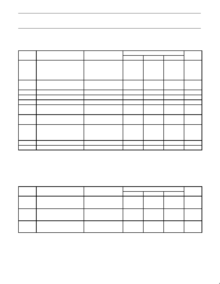
DC ELECTRICAL CHARACTERISTICS
T
A
=+25
∞
C
V
SS
=
±
6V, V
CM
=0, unless otherwise specified. Recommended operating supply voltages V
S
=
±
6.0V. All specifications apply to both
standard and high gain parts unless noted differently.
SYMBOL
PARAMETER
TEST CONDITIONS
NE592
UNIT
SYMBOL
PARAMETER
TEST CONDITIONS
Min
Typ
Max
UNIT
A
VOL
Differential voltage gain,
standard part
Gain 1
1
R
L
=2k
, V
OUT
=3V
P-P
250
400
600
V/V
Gain 2
2, 4
80
100
120
V/V
R
IN
Input resistance
Gain 1
1
4.0
k
Gain 2
2, 4
10
30
k
C
IN
Input capacitance
2
Gain 2
4
2.0
pF
I
OS
Input offset current
0.4
5.0
µ
A
I
BIAS
Input bias current
9.0
30
µ
A
V
NOISE
Input noise voltage
BW 1kHz to 10MHz
12
µ
V
RMS
V
IN
Input voltage range
±
1.0
V
CMRR
Common-mode rejection ratio
Gain 2
4
V
CM
±
1V, f<100kHz
60
86
dB
Gain 2
4
V
CM
±
1V, f=5MHz
60
dB
PSRR
Supply voltage rejection ratio
Gain 2
4
V
S
=
±
0.5V
50
70
dB
V
OS
Output offset voltage
Gain 1
R
L
=
1.5
V
Gain 2
4
R
L
=
1.5
V
Gain 3
3
R
L
=
0.35
0.75
V
V
CM
Output common-mode voltage
R
L
=
2.4
2.9
3.4
V
V
OUT
Output voltage swing
R
L
=2k
3.0
4.0
V
differential
R
OUT
Output resistance
20
I
CC
Power supply current
R
L
=
18
24
mA
NOTES:
1. Gain select Pins G
1A
and G
1B
connected together.
2. Gain select Pins G
2A
and G
2B
connected together.
3. All gain select pins open.
4. Applies to 14-pin version only.
Philips Semiconductors RF Communications Products
Product specification
NE592
Video amplifier
April 15, 1992
253
DC ELECTRICAL CHARACTERISTICS
DC Electrical CharacteristicsV
SS
=
±
6V, V
CM
=0, 0
∞
C
T
A
70
∞
C, unless otherwise specified. Recommended operating supply voltages V
S
=
±
6.0V.
All specifications apply to both standard and high gain parts unless noted differently.
SYMBOL
PARAMETER
TEST CONDITIONS
NE592
UNIT
SYMBOL
PARAMETER
TEST CONDITIONS
Min
Typ
Max
UNIT
A
VOL
Differential voltage gain,
standard part
Gain 1
1
R
L
=2k
, V
OUT
=3V
P-P
250
600
V/V
Gain 2
2, 4
80
120
V/V
R
IN
Input resistance
Gain 2
2, 4
8.0
k
I
OS
Input offset current
6.0
µ
A
I
BIAS
Input bias current
40
µ
A
V
IN
Input voltage range
±
1.0
V
CMRR
Common-mode rejection ratio
Gain 2
4
V
CM
±
1V, f<100kHz
50
dB
PSRR
Supply voltage rejection ratio
Gain 2
4
V
S
=
±
0.5V
50
dB
V
OS
Output offset voltage
Gain 1
Gain 2
4
Gain 3
3
R
L
=
1.5
1.5
1.0
V
V
OUT
Output voltage swing differential
R
L
=2k
2.8
V
I
CC
Power supply current
R
L
=
27
mA
NOTES:
1. Gain select Pins G
1A
and G
1B
connected together.
2. Gain select Pins G
2A
and G
2B
connected together.
3. All gain select pins open.
4. Applies to 14-pin versions only.
AC ELECTRICAL CHARACTERISTICS
T
A
=+25
∞
C
V
SS
=
±
6V, V
CM
=0, unless otherwise specified. Recommended operating supply voltages V
S
=
±
6.0V. All specifications apply to both
standard and high gain parts unless noted differently.
SYMBOL
PARAMETER
TEST CONDITIONS
NE/SA592
UNIT
Min
Typ
Max
BW
Bandwidth
Gain 1
1
Gain 2
2, 4
40
90
MHz
MHz
t
R
Rise time
Gain 1
1
Gain 2
2, 4
V
OUT
=1V
P-P
10.5
4.5
12
ns
ns
t
PD
Propagation delay
Gain 1
1
Gain 2
2, 4
V
OUT
=1V
P-P
7.5
6.0
10
ns
ns
NOTES:
1. Gain select Pins G
1A
and G
1B
connected together.
2. Gain select Pins G
2A
and G
2B
connected together.
3. All gain select pins open.
4. Applies to 14-pin versions only.
Philips Semiconductors RF Communications Products
Product specification
NE592
Video amplifier
April 15, 1992
254
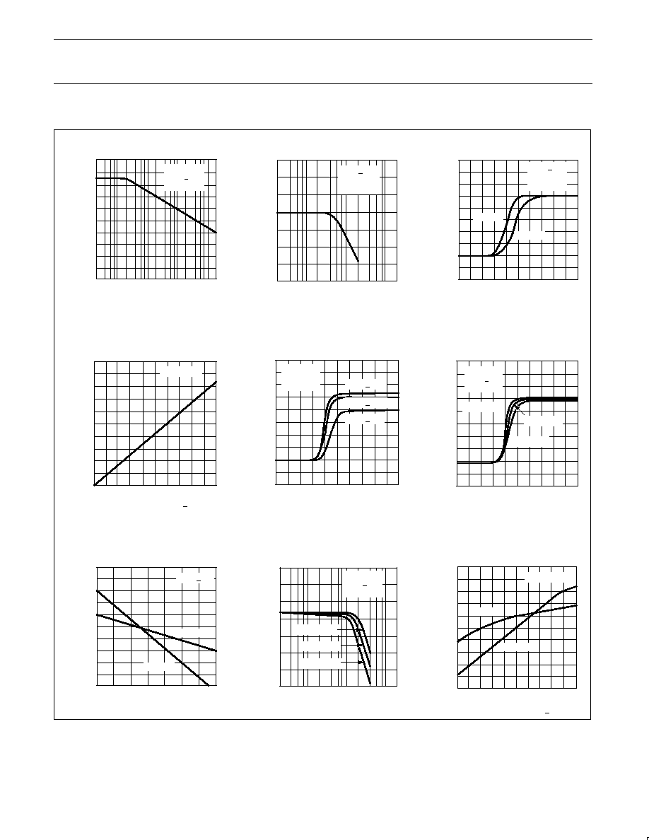
TYPICAL PERFORMANCE CHARACTERISTICS
TA = 70
o
C
Tamb = 0
o
C
COMMON-MODE REJECTION RA
TIO ≠ dB
OUTPUT VOL
T
AGE ≠ V
OUTPUT VOL
T
AGE ≠ V
SINGLE ENDED VOL
T
AGE GAIN ≠ dB
RELA
TIVE VOL
T
AGE GAIN
RELA
TIVE VOL
T
AGE GAIN
OUTPUT VOL
T
AGE ≠ V
OUTPUT VOL
T
AGE SWING ≠ Vpp
Common-Mode Rejection Ratio
as a Function of Frequency
Output Voltage Swing as
a Function of Frequency
Pulse Response
Supply Current as a
Function of Temperature
Pulse Response as a
Function of Supply Voltage
Pulse Response as a
Function of Temperature
Voltage Gain as a
Function of Temperature
Gain vs. Frequency as a
Function of Temperature
Voltage Gain as a
Function of Supply Voltage
100
90
80
70
60
50
40
30
20
10
0
10k
100k
1M
10M
100M
7.0
6.0
5.0
4.0
3.0
2.0
1.0
0
1
5
10
50 100
500 1000
1.6
1.4
1.2
1.0
0.8
0.6
0.4
0.2
0
-0.2
-0.4
-15 -10 -5
0
5
10 15 20 25 30 35
1.6
1.4
1.2
1.0
0.8
0.6
0.4
0.2
0
-0.2
-0.4
-15 -10 -5
0
5
10 15 20 25 30 35
1.6
1.4
1.2
1.0
0.8
0.6
0.4
0.2
0
-0.2
-0.4
-15 -10 -5
0
5
10 15 20 25 30 35
1.10
1.08
1.06
1.04
1.02
1.00
0.98
0.96
0.94
0.92
0.90
0
10
20
30
40
50
60
70
60
50
40
30
20
10
0
-10
1
5
10
50 100
500 1000
1.4
1.3
1.2
1.1
1.0
0.9
0.8
0.7
0.6
0.5
0.4
3
4
5
6
7
8
FREQUENCY ≠ Hz
FREQUENCY ≠ MHz
TIME ≠ ns
TIME ≠ ns
TIME ≠ ns
FREQUENCY ≠ MHz
SUPPLY VOLTAGE ≠ +V
TEMPERATURE ≠
o
C
GAIN 2
VS = +6V
TA = 25
o
C
VS = +6V
TA = 25
o
C
RL = 1k
VS = +6V
TA = 25
o
C
RL = 1k
GAIN 2
TA = 25
o
C
RL = 1k
GAIN 2
VS = +6V
RL = 1k
VS = +6V
GAIN 2
VS = +6V
RL = 1k
Tamb = 25
o
C
GAIN 2
GAIN 1
VS = +8V
VS = +3V
VS = +6V
TA = 25
o
C
GAIN 2
GAIN 1
TA = 125
o
C
TA = ≠55
o
C
TA = 25
o
C
GAIN 2
GAIN 1
SUPPL
Y
CURRENT ≠ mA
28
24
20
16
12
8
3
4
5
6
7
8
SUPPLY VOLTAGE ≠ +V
TA = 25
o
C
Philips Semiconductors RF Communications Products
Product specification
NE592
Video amplifier
April 15, 1992
255
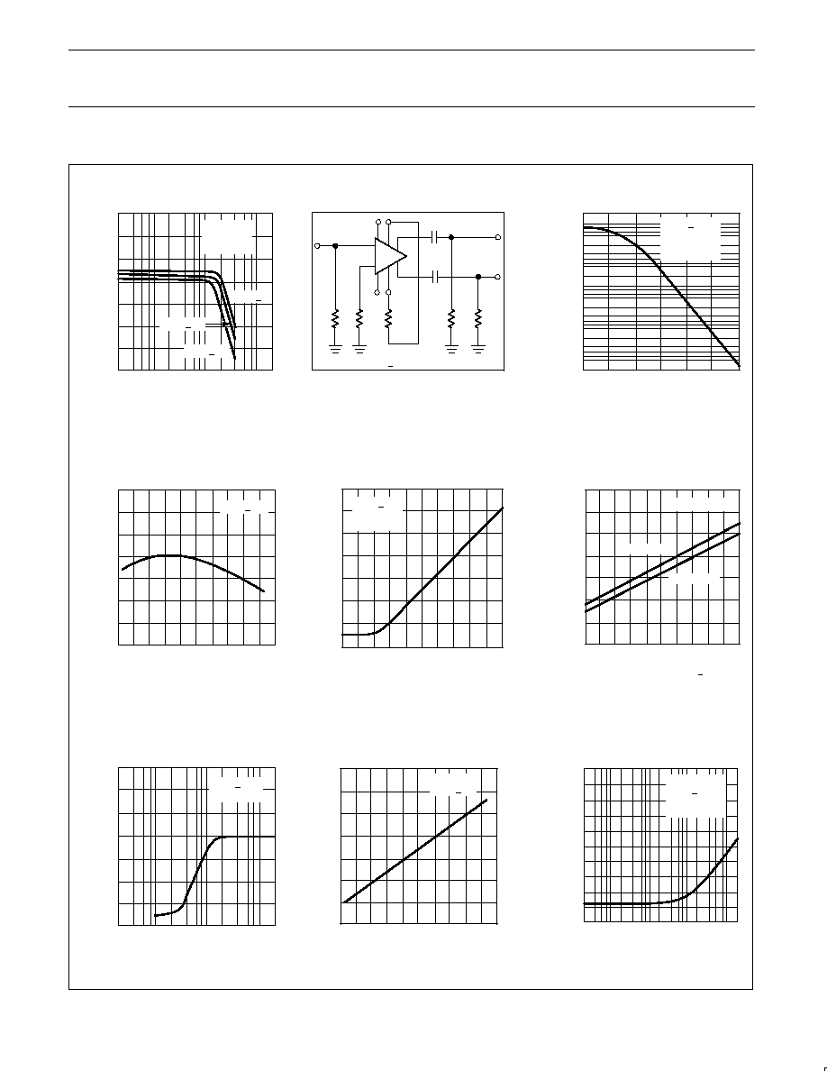
TYPICAL PERFORMANCE CHARACTERISTICS
(Continued)
SINGLE ENDED VOL
T
AGE GAIN ≠ dB
DIFFERENTIAL
VOL
T
AGE GAIN ≠ V/V
SUPPL
Y
CURRENT ≠ mA
OUTPUT VOL
T
AGE SWING ≠ V OR
OUTPUT SINK CURRENT ≠ mA
OUTPUT VOL
T
AGE SWING ≠ Vpp
INPUT RESIST
ANCE ≠ K
INPUT NOISE VOL
T
AGE ≠ V
rms
Gain vs. Frequency as a
Function of Supply Voltage
Voltage Gain
Adjust Circuit
Voltage Gain as a
Function of RADJ (Figure 3)
Supply Current as a
Function of Temperature
Differential Overdrive
Recovery Time
Output Voltage and Current
Swing as a Function of
Supply Voltage
Output Voltage Swing as a
Function of Load Resistance
Input Resistance as a
Function of Temperature
Input Noise Voltage
as a Function of
Source Resistance
60
50
40
30
20
10
0
-10
1
5
10
50 100
500 1000
1000
100
10
1
.1
.01
1
10
100
1K
10K 100K
1M
21
20
19
18
17
16
15
14
-60
-20
20
60
100
140
7.0
6.0
5.0
4.0
3.0
2.0
1.0
0
3.0
4.0
5.0
6.0
7.0
8.0
7.0
6.0
5.0
4.0
3.0
2.0
1.0
0
10
50 100
500 1K
5K 10K
70
60
50
40
30
20
10
0
-60
-20
0
20
60
100
140
100
90
80
70
60
50
40
30
20
10
0
1
10
100
1K
10K
FREQUENCY ≠ MHz
RADJ ≠
TEMPERATURE ≠
o
C
SUPPLY VOLTAGE ≠ +V
LOAD RESISTANCE ≠
TEMPERATURE ≠
o
C
SOURCE RESISTANCE ≠
VS = +8V
VS = +3V
VS = +6V
GAIN 2
TA = 25
o
C
RL = 1k
VS = +6V
f = 100kHz
TA = 25
o
C
FIGURE 3
VS = +6V
TA = 25
o
C
VS = +6V
TA = 25
o
C
GAIN 2
VS = +6V
GAIN 2
VS = +6V
TA = 25
o
C
BW = 10MHz
VOLTAGE
CURRENT
14
1
12
11
8
7
4
3
0.2
µ
F
0.2
µ
F
592
51
51
R
ADJ
1k
1k
TA = 25
o
C
VS = +6V
OVERDRIVE RECOVER
Y
TIME ≠ ns
70
60
50
40
30
20
10
0
0
20 40 60
80 100 120 140 160 180 200
DIFFERENTIAL INPUT VOLTAGE ≠ mV
VS = +6V
TA = 25
o
C
GAIN 2
µ
Philips Semiconductors RF Communications Products
Product specification
NE592
Video amplifier
April 15, 1992
256
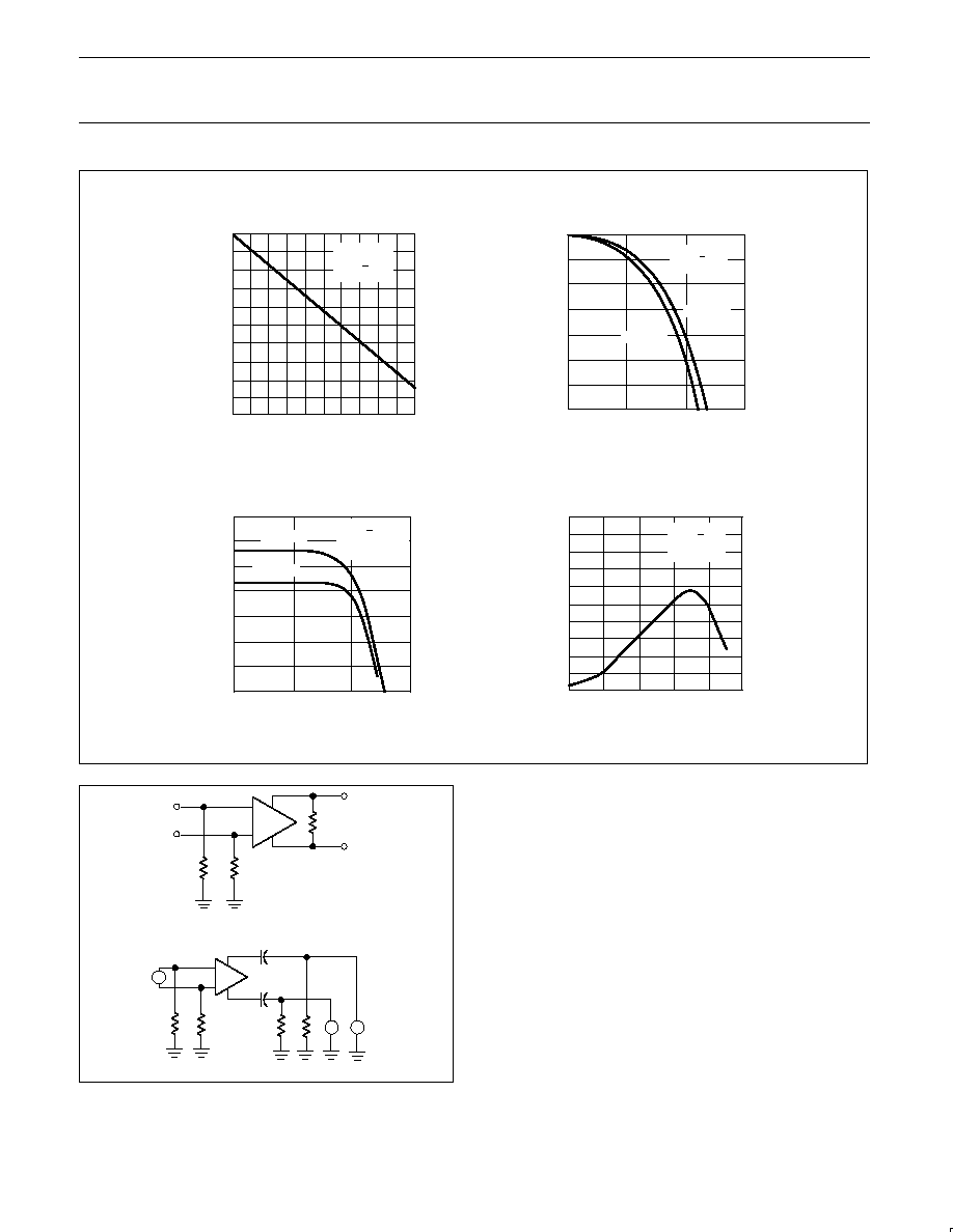
PHASE SHIFT ≠ DEGREES
PHASE SHIFT ≠ DEGREES
VOL
T
AGE GAIN ≠ dB
VOL
T
AGE GAIN ≠ dB
Phase Shift as a
Function of Frequency
Phase Shift as a
Function of Frequency
Voltage Gain as a
Function of Frequency
Voltage Gain as a
Function of Frequency
0
-5
-10
-15
-20
-25
0
1
2
3
4
5
6
7
8
9
10
0
-50
-100
-150
-200
-250
-300
-350
1
10
100
1000
60
50
40
30
20
10
0
1
10
100
1000
.01
.1
1
10
100
1000
40
30
20
10
0
-10
-20
-30
-40
-50
FREQUENCY ≠ MHz
FREQUENCY ≠ MHz
FREQUENCY ≠ MHz
FREQUENCY ≠ MHz
VS = +6V
TA = 25
o
C
GAIN 2
VS = +6V
TA = 25
o
C
VS = +6V
Tamb = 25
o
C
RL = 1K
VS = +6V
TA = 25
o
C
GAIN 3
GAIN 1
GAIN 2
GAIN 1
GAIN 2
TEST CIRCUITS
T
A
= 25
∞
C, unless otherwise specified.
VIN
VOUT
RL
592
51
51
51
51
e
in
e
out
e
out
1k
1k
0.2
µ
F
0.2
µ
F
592
Philips Semiconductors RF Communications Products
Product specification
NE592
Video amplifier
April 15, 1992
257
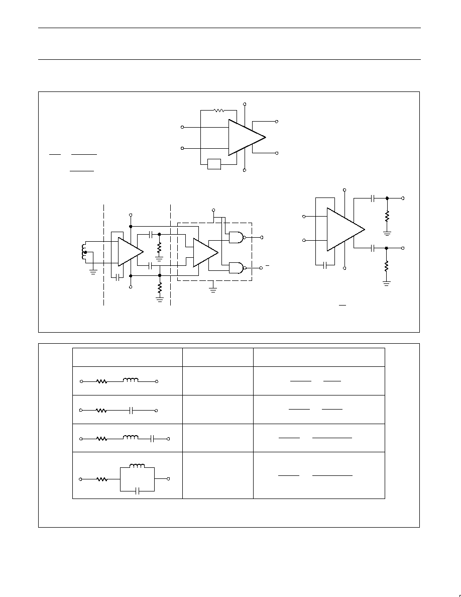
TYPICAL APPLICATIONS
NOTE:
Basic Configuration
Disc/Tape Phase-Modulated Readback Systems
Differentiation with High
Common-Mode Noise Rejection
NOTE:
For frequency F
1
<< 1/2
(32) C
V
O
]
1.4 x 10⁴C
dVi
dT
Z
V1
2re
+6
V0
7
5
4
1
14
11
10
-6
592
READ HEAD
DIFFERENTIATOR/AMPLIFIER
ZERO CROSSING DETECTOR
+5
9
4
8
529
7
5
Q
Q
6
3
2
1
10
+6
14
11
10
8
7
5
4
1
-6
AMPLITUDE:
1-10 mV p-p
FREQUENCY: 1-4 MHz
592
0.2
µ
F
+6
0.2
µ
F
2K
2K
V0
V1
C
14
1
11
4
10
5
7
8
-6
592
V
0
(s)
v
1
(s)
[
1.4
@
104
Z(S)
)
2re
[
1.4
@
104
Z(S)
)
32
FILTER NETWORKS
NOTES:
In the networks above, the R value used is assumed to include 2re, or approximately 32
.
S = j
= 2
f
1.4
104
L
1
s
)
R L
1.4
104
R
s
s
)
1 RC
1.4
104
L
s
s2
)
R Ls
)
1 LC
1.4
104
R
s2
)
1 LC
s2
)
1 LC
)
s RC
Z NETWORK
FILTER
TYPE
V0 (s) TRANSFER
V1 (s) FUNCTION
LOW PASS
HIGH PASS
BAND PASS
BAND REJECT
R
L
R
C
R
L
C
R
L
C