
Philips Semiconductors Linear Products
Product specification
NE/SE5514
Quad high-performance operational amplifier
82
August 31, 1994
853-1175 13721
DESCRIPTION
The NE/SE5514 family of quad operational amplifiers sets new
standards in bipolar quad amplifier performance. The amplifiers
feature low input bias current and low offset voltages. Pinout is
identical to LM324/LM348 which facilitates direct product
substitution for improved system performance in dual supply
applications. Output characteristics are similar to a
µ
A741 with
improved slew and drive capability.
FEATURES
∑
Low input bias current: <
±
3nA
∑
Low input offset current: <
±
3nA
∑
Low input offset voltage:<1mV
∑
Low supply current: 1.5mA/A
∑
1V/
µ
s slew rate
∑
High input impedance: 100M
∑
High common-mode impedance: 10G
∑
Internal compensation for unity gain
∑
600
drive capability (7V
RMS
)
APPLICATIONS
∑
AC amplifiers
∑
RC active filters
∑
Transducer amplifiers
∑
DC gain block
∑
Instrumentation amplifier
PIN CONFIGURATIONS
N Packages
D Package
1
NOTE:
1. SOL - Released in 16-lead large SO package
only. Pinout is different than N package.
1
2
3
4
5
6
7
8
14
13
12
11
10
9
1
2
3
4
5
6
7
8
9
10
11
12
13
14
16
15
OUTPUT 1
≠INPUT 1
V+
+INPUT 2
OUTPUT 2
+INPUT 1
≠INPUT 2
OUTPUT 1
≠INPUT 1
V≠
+INPUT 2
OUTPUT 2
+INPUT 1
≠INPUT 2
OUTPUT 1
≠INPUT 1
V+
+INPUT 2
OUTPUT 2
+INPUT 1
≠INPUT 2
OUTPUT 1
≠INPUT 1
V≠
+INPUT 2
OUTPUT 2
+INPUT 1
≠INPUT 2
NC
NC
1
2
3
4
1
2
3
4
ORDERING INFORMATION
DESCRIPTION
TEMPERATURE RANGE
ORDER CODE
DWG #
16-Pin Plastic Small Outline Large (SOL) package
0 to +70
∞
C
NE5514D
0171B
14-Pin Plastic Dual In-Line Package (DIP)
0 to +70
∞
C
NE5514N
0405B
14-Pin Plastic Dual In-Line Package (DIP)
-55 to +125
∞
C
SE5514N
0405B

Philips Semiconductors Linear Products
Product specification
NE/SE5514
Quad high-performance operational amplifier
August 31, 1994
83
EQUIVALENT SCHEMATIC
≠VIN
+VIN
(ONE OP AMP)
V+
OUTPUT
≠V
ABSOLUTE MAXIMUM RATINGS
SYMBOL
PARAMETER
RATING
UNIT
V
CC
Supply voltage
±
16
V
V
DIFF
Differential input voltage
32
V
V
IN
Input voltage
0 to 32
V
Output short to ground
Continuous
T
STG
Storage temperature range
-65 to +150
∞
C
T
SOLD
Lead soldering temperature (10sec max)
300
∞
C
T
A
Operating ambient temperature range
NE5514
0 to 70
∞
C
SE5514
-55 to +125
∞
C
P
MAX
Maximum power dissipation
T
A
=25
∞
C (still-air)
1
N package
1420
mW
D package
1250
mW
NOTES:
1. The following derating factors should be applied above 25
∞
C
N package at 11.4mW/
∞
C
D package at 10.0mW/
∞
C
Philips Semiconductors Linear Products
Product specification
NE/SE5514
Quad high-performance operational amplifier
August 31, 1994
84
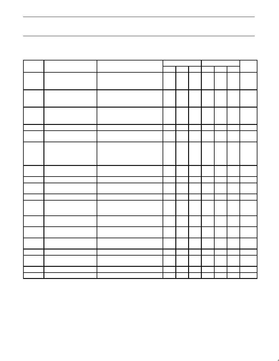
ELECTRICAL CHARACTERISTICS
V
CC
=
±
15V, T
A
= 25
∞
C unless otherwise specified.
SYMBOL
PARAMETER
TEST CONDITIONS
SE5514
NE5514
UNIT
SYMBOL
PARAMETER
TEST CONDITIONS
Min
Typ
Max
Min
Typ
Max
UNIT
V
OS
Input offset voltage
R
S
=100
, T
A
=+25
∞
C
Over temp.
0.7
1
2
3
1
1.5
5
6
mV
V
OS
Over temp.
4
5
µ
V/
∞
C
I
OS
Input offset current
R
S
=100k
, T
A
=+25
∞
C
Over temp.
3
4
10
20
6
8
20
30
nA
I
OS
Over temp.
30
40
pA/
∞
C
I
BIAS
Input bias current
R
S
=100k
, T
A
=+25
∞
C
Over temp.
3
4
10
20
6
8
20
30
nA
I
BIAS
Over temp.
30
40
pA/
∞
C
R
IN
Input resistance differential
T
A
=25
∞
C
100
100
M
V
CM
Input common mode range
T
A
=25
∞
C
Over temp.
±
13.5
±
13
±
13.7
±
13.2
±
13.5
±
13
±
13.7
±
13.2
V
V
CC
=
±
15V,
CMRR
Input common-mode rejection
ratio
V
IN
=
±
13.5V @ T
A
=25
∞
C
70
100
70
100
dB
V
IN
=
±
13V @ Over temp.
A
V
Large-signal voltage gain
R
L
=2k
, T
A
=25
∞
C
V
O
=
±
10V, Over temp.
50
25
200
50
25
200
V/mV
SR
Slew rate
T
A
=25
∞
C
0.6
1
0.6
1
V/
µ
s
GBW
Small-signal unity gain band-
width
T
A
=25
∞
C
3
3
MHz
M
Phase margin
T
A
=25
∞
C
45
45
Deg
V
OUT
Output voltage swing
R
L
=2k
, T
A
=25
∞
C
Over temp.
±
13
±
12.5
±
13.5
±
13
±
13
±
12.5
±
13.5
±
13
V
V
OUT
Output voltage swing
R
L
=600
1
, T
A
=25
∞
C
Over temp.
±
10
±
7.5
±
11.5
±
9
±
10
±
8
±
11.5
±
9
V
I
CC
Power supply current
R
L
=Open, T
A
=25
∞
C
Over temp.
6
7
10
12
6
7
10
12
mA
PSRR
Power supply rejection ratio
±
5V
V
CC
±
15V
Over temp.
80
110
80
110
dB
AA
Amplifier to amplifier coupling
f=1kHz to 20kHz, T
A
=25
∞
C
-120
-120
dB
THD
Total harmonic distortion
f=10kHz, T
A
=25
∞
C
V
O
=7V
RMS
0.01
0.01
%
V
NOISE
Input noise voltage
f=1kHz, T
A
=25
∞
C
30
30
nV/
Hz
I
SC
Short-circuit current
T
A
=25
∞
C
10
40
60
10
40
60
mA
NOTES:
1. Not to exceed maximum power dissipation.