 | –≠–ª–µ–∫—Ç—Ä–æ–Ω–Ω—ã–π –∫–æ–º–ø–æ–Ω–µ–Ω—Ç: OM4031T | –°–∫–∞—á–∞—Ç—å:  PDF PDF  ZIP ZIP |
Document Outline
- FEATURES
- APPLICATIONS
- GENERAL DESCRIPTION
- QUICK REFERENCE DATA
- ORDERING INFORMATION
- BLOCK DIAGRAM
- PINNING
- FUNCTIONAL DESCRIPTION
- Moving average noise filter
- Filter implementation
- Filter characteristic
- Noise reduction
- OPERATING INSTRUCTIONS
- Control signals
- Power-down mode
- Reset
- LIMITING VALUES
- DC CHARACTERISTICS
- AC CHARACTERISTICS
- APPLICATION INFORMATION
- PACKAGE OUTLINE
- SOLDERING
- DEFINITIONS
- LIFE SUPPORT APPLICATIONS

DATA SHEET
Preliminary specification
File under Integrated Circuits, IC03
October 1994
INTEGRATED CIRCUITS
Philips Semiconductors
OM4031T
Digital post-detection filter
for FSK data receivers

October 1994
2
Philips Semiconductors
Preliminary specification
Digital post-detection filter
for FSK data receivers
OM4031T
FEATURES
∑
External clock frequency 30 to 80 kHz (typ. 38.4 kHz)
∑
Supported data rates 600, 1200, 2400 and 4800 bits/s
(typ.)
∑
Double bandwidth option (not for 4800 bits/s)
∑
Schmitt-triggered inputs for optimum slope tolerance
∑
Enable input for power-down mode
∑
Open-drain output (3-state in power-down mode)
∑
No external components required
∑
Single supply voltage from 1.8 to 6.0 V
∑
Very low operating current (1.5
µ
A typ.)
∑
Operating temperature from
-
10 to +70
∞
C.
APPLICATIONS
∑
Telemetry data receivers
∑
RF security systems
∑
Low-bit-rate radio data links
∑
Paging applications of UAA2080 and UAA2082 with
software decoding.
GENERAL DESCRIPTION
The OM4031T is intended for performance enhancement
of FSK data receivers that do not have a built-in
post-detection filter.
It contains a digital moving average filter to remove noise
from the demodulated data. When operated from a
38.4 kHz external clock it can handle data rates of 600,
1200 and 2400 bits/s at an oversampling rate of 16. The
filter bandwidth can be doubled to ease the search for bit
synchronization on the output data.
To allow for jitter in the input data, a 12-bit sample is taken
for the majority decision. Doubling the filter bandwidth is
realised by taking the majority out of 6 samples
(2400 bits/s) or by doubling the sampling rate (600 and
1200 bits/s).
An input data rate of 4800 bits/s is supported at 8 times
oversampling and normal bandwidth.
All inputs are Schmitt-triggered to ensure reliable
operation even at signals with long rise/fall times.
QUICK REFERENCE DATA
Notes
1. V
DD
= 2.0 V; DOUT open-circuit; input data at 20 kHz random pattern.
2. Bench evaluated for UAA2080H at 470 MHz, not factory tested.
ORDERING INFORMATION
SYMBOL
PARAMETER
CONDITIONS
MIN.
TYP.
MAX.
UNIT
V
DD
supply voltage
1.8
-
6.0
V
I
DDPD
power-down supply current
CE = V
SS
-
1.0
10.0
µ
A
I
DD
operating supply current
CE = V
DD
; note 1
-
1.5
20.0
µ
A
P
i(ref)
sensitivity improvement at 3% bit error rate note 2
600 bits/s, 250
µ
s slope
-
5.3
-
dB
1200 bits/s, 250
µ
s slope
-
3.6
-
dB
2400 bits/s, 125
µ
s slope
-
2.0
-
dB
T
amb
operating ambient temperature
-
10
-
+70
∞
C
TYPE NUMBER
PACKAGE
NAME
DESCRIPTION
VERSION
OM4031T
SO8
plastic small outline package; 8 leads; body width 3.9 mm
SOT96-1
October 1994
3
Philips Semiconductors
Preliminary specification
Digital post-detection filter
for FSK data receivers
OM4031T
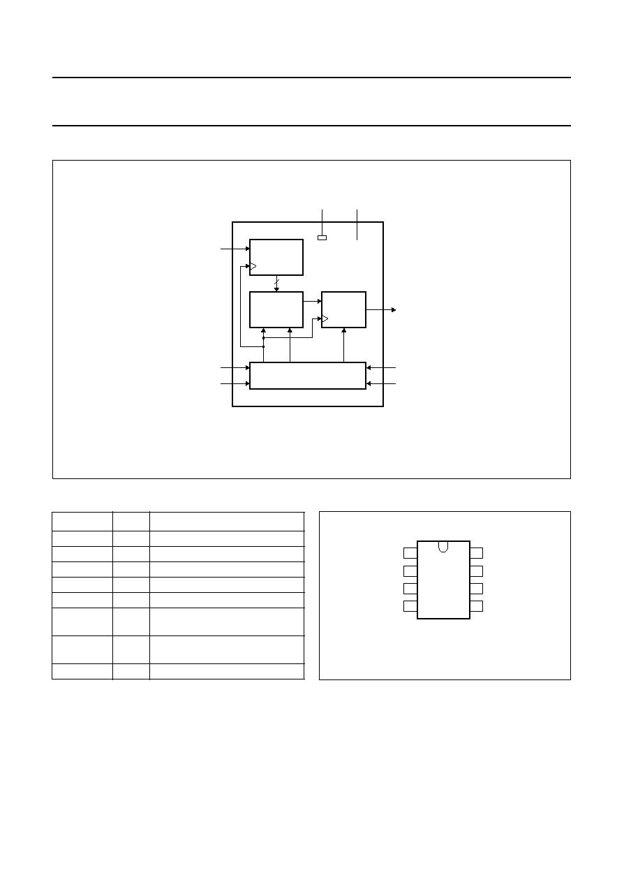
BLOCK DIAGRAM
Fig.1 Block diagram.
handbook, full pagewidth
MLC273
MAJORITY
LOGIC
13-BIT SHIFT
REGISTER
OM4031T
OUTPUT
LATCH
DATA RATE AND
BANDWIDTH CONTROL
CINT
DBW
PDN
1
DIN
3
CLK
2
CE
7
A1
6
A0
5
DOUT
8
SS
4
V
DD
V
PINNING
SYMBOL
PIN
DESCRIPTION
DIN
1
data input
CE
2
chip enable input
CLK
3
external clock input
V
SS
4
negative supply voltage
DOUT
5
data output (open-drain)
A0
6
data rate and bandwidth control
input 0 (see Table 1)
A1
7
data rate and bandwidth control
input 1 (see Table 1)
V
DD
8
positive supply voltage
Fig.2 Pin configuration.
handbook, halfpage
1
2
3
4
8
7
6
5
MLC274
OM4031T
VDD
VSS
A1
A0
DOUT
CLK
CE
DIN

October 1994
4
Philips Semiconductors
Preliminary specification
Digital post-detection filter
for FSK data receivers
OM4031T
FUNCTIONAL DESCRIPTION
The OM4031T digital post-detection filter oversamples the
noisy binary data stream at input DIN (pin 1), and outputs
a noise-reduced data stream via open-drain output DOUT
(pin 5). The filter bandwidth can be doubled to ease the
search for bit synchronization on the data output signal.
Input sampling takes place at 16 times the data rate. For a
typical clock frequency of 38.4 kHz the nominal data rates
are 600, 1200 and 2400 bits/s. A data rate of 4800 bits/s
can be handled at an oversampling rate of 8 and at normal
bandwidth only.
Using a different clock frequency will produce bit rates
equal to the clock frequency divided by 64, 32 or 16. When
the clock frequency is not an integer multiple of the data
rate some edge jitter will be introduced in the output data.
The clock frequency is not very critical for the noise filtering
performance: a clock frequency of 32.768 kHz could be
used at 512, 1200 and 2400 bits/s without loss of
performance.
Since no on-chip oscillator is available an external clock
signal is required at input CLK (pin 3). Two control inputs
A0 and A1 (pins 6 and 7) are used for selection of the data
rate and the filter bandwidth.
A separate enable input CE (pin 2) allows the circuit to be
powered down. In power-down mode (CE = LOW) the
system clock is inhibited and the data output DOUT is
made 3-state and remains static.
Moving average noise filter
Noise reduction is achieved by applying a moving average
filter on N samples of the input data signal. In principle N
can be odd or even, but in the OM4031T an even number
is used (N = 12). When there is no absolute majority (equal
number of ones and zeroes) the previous majority output
is maintained.
An odd value for N would always produce an absolute
majority and not require decision feedback. However the
noise performance is worse for odd values of N, because
the output can toggle at every clock (e.g. when a 101010...
pattern is clocked in). For even values of N the output
polarity can only change once every 3 clocks and does not
toggle at all for a 101010... or a 11001100... pattern.
Using 12 out of 16 samples for the majority decision
produces a filter which combines good noise reduction
with a large tolerance for data jitter (maximum
1
/
8
-bit
duration).
Filter implementation
The moving average filter is implemented using a 13-bit
register and two state machines (COUNT and CLOCK) for
the majority decision. The first stage of the shift register is
used for input synchronization.
The CLOCK state machine generates the internal clock
signal CINT and the bandwidth selection signal DBW in
accordance with the logic levels on control lines CE, A0
and A1.
The majority decision is taken by state machine COUNT
based on the contents of the input shift register and the
previous decision in the output latch.
The doubled bandwidth is achieved by increasing the
sampling rate by a factor of 2 for 600 and 1200 bits/s. For
2400 bits/s the number of samples for the majority
decision is halved, controlled by the DBW signal. This
signal is derived from the control signals as follows:
DBW
CE
A0
∑
A1
∑
=

October 1994
5
Philips Semiconductors
Preliminary specification
Digital post-detection filter
for FSK data receivers
OM4031T
Filter characteristic
The frequency characteristic of the moving average filter in
the OM4031T is given in Fig.3 for N = 12 and N = 6.
The horizontal axis shows the normalized frequency f
N
which is the ratio of the frequency f and the sampling
frequency f
s
. The value for f
s
is given in Table 1 for the
various data rates and filter bandwidths.
The vertical axis shows the normalized amplitude A
N
.
At normal bandwidth the oversampling rate is 16, except
for 4800 bits/s where it is 8. At double bandwidth the
oversampling rate is 32, except for 2400 bits/s,
where it is 16.
The 3 dB cut-off frequency is calculated as follows:
N = 12:
N = 6:
f
co
0.0371
f
s
◊
=
f
co
0.0748
f
s
◊
=
Fig.3 Filter transfer function of the OM4031T.
handbook, full pagewidth
0.5
1.0
0
0
0.1
0.2
0.3
0.4
MLC275
0.2
0.4
0.6
0.8
fN
A N
(1)
(2)
(1) N = 12.
(2) N = 6.