Document Outline
- FEATURES
- GENERAL DESCRIPTION
- ORDERING INFORMATION
- BLOCK DIAGRAM
- PINNING
- FUNCTIONAL DESCRIPTION
- I 2 C-BUS DESCRIPTION
- LIMITING VALUES
- HANDLING
- DC CHARACTERISTICS
- AC CHARACTERISTICS
- CHIP DIMENSIONS AND BONDING PAD LOCATIONS
- PACKAGE OUTLINE
- SOLDERING
- DEFINITIONS
- LIFE SUPPORT APPLICATIONS
- PURCHASE OF PHILIPS I2C COMPONENTS

DATA SHEET
Product specification
Supersedes data of 1996 Nov 14
File under Integrated Circuits, IC12
1997 Feb 25
INTEGRATED CIRCUITS
OM4085
Universal LCD driver for low
multiplex rates

1997 Feb 25
2
Philips Semiconductors
Product specification
Universal LCD driver for low multiplex
rates
OM4085
FEATURES
∑
Single-chip LCD controller/driver
∑
Selectable backplane drive configuration: static
or 2, 3 or 4 backplane multiplexing
∑
Selectable display bias configuration: static,
1
/
2
or
1
/
3
∑
Internal LCD bias generation with voltage-follower
buffers
∑
24 segment drives: up to twelve 8-segment numeric
characters; up to six 15-segment alphanumeric
characters; or any graphics of up to 96 elements
∑
24
◊
4-bit RAM for display data storage
∑
Auto-incremented display data loading across device
subaddress boundaries
∑
Display memory bank switching in static and duplex
drive modes
∑
Versatile blinking modes
∑
LCD and logic supplies may be separated
∑
2.0 to 6 V power supply range
∑
Low power consumption
∑
Power saving mode for extremely low power
consumption in battery-operated and telephone
applications
∑
I
2
C-bus interface
∑
TTL/CMOS compatible
∑
Compatible with any 4-bit, 8-bit or 16-bit
microprocessors/microcontrollers
∑
May be cascaded for large LCD applications
(up to 1536 segments possible)
∑
Cascadable with the 40 segment LCD driver PCF8576C
∑
Optimized pinning for single plane wiring in both single
and multiple OM4085 applications
∑
Space-saving 40 lead plastic very small outline package
(VSO40; SOT158-1)
∑
No external components required (even in multiple
device applications)
∑
Manufactured in silicon gate CMOS process.
GENERAL DESCRIPTION
The OM4085 is a peripheral device which interfaces to
almost any Liquid Crystal Display (LCD) having low
multiplex rates. It generates the drive signals for any static
or multiplexed LCD containing up to four backplanes and
up to 24 segments and can easily be cascaded for larger
LCD applications. The OM4085 is compatible with most
microprocessors/microcontrollers and communicates via a
two-line bidirectional I
2
C-bus. Communication overheads
are minimized by a display RAM with auto-incremented
addressing, by hardware subaddressing and by display
memory switching (static and duplex drive modes).
ORDERING INFORMATION
TYPE NUMBER
PACKAGE
NAME
DESCRIPTION
VERSION
OM4085T
VSO40
plastic very small outline package; 40 leads
SOT158-1
1997
Feb
25
3
Philips Semiconductors
Product specification
Universal LCD driver for low multiplex
rates
OM4085
This text is here in white to force landscape pages to be rotated correctly when browsing through the pdf in the Acrobat reader.This text is here in
_
white to force landscape pages to be rotated correctly when browsing through the pdf in the Acrobat reader.This text is here inThis text is here in
white to force landscape pages to be rotated correctly when browsing through the pdf in the Acrobat reader. white to force landscape pages to be ...
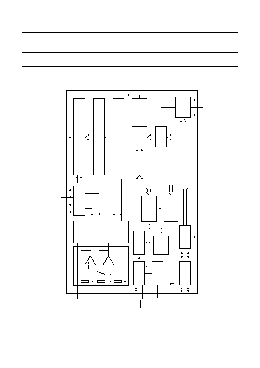
BLOCK DIAGRAM
handbook, full pagewidth
MGD866
LCD
VOLTAGE
SELECTOR
12
5
TIMING
BLINKER
OSCILLATOR
INPUT
FILTERS
I C-BUS
CONTROLLER
2
POWER-
ON
RESET
CLK
4
SYNC
3
OSC
6
11
SCL
2
SDA
1
SA0
10
DISPLAY
CONTROLLER
COMMAND
DECODER
BACKPLANE
OUTPUTS
13
BP0
14
BP2
15
BP1
16
BP3
INPUT
BANK
SELECTOR
DISPLAY
RAM
24
◊
4 BITS
OUTPUT
BANK
SELECTOR
DATA
POINTER
SUB-
ADDRESS
COUNTER
DISPLAY SEGMENT OUTPUTS
DISPLAY LATCH
SHIFT REGISTER
17 to 40
S0 to S23
A0
7
A1
8
A2
9
OM4085
LCD BIAS
GENERATOR
VSS
VLCD
VDD
R
R
R
Fig.1 Block diagram.
1997 Feb 25
4
Philips Semiconductors
Product specification
Universal LCD driver for low multiplex
rates
OM4085
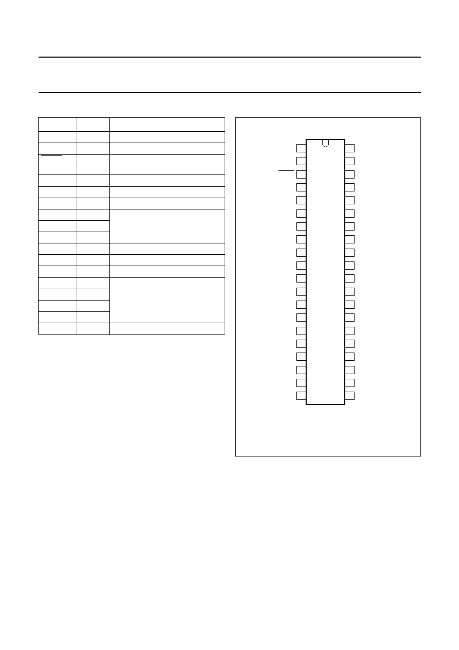
PINNING
SYMBOL
PIN
DESCRIPTION
SDA
1
I
2
C-bus data input/output
SCL
2
I
2
C-bus clock input/output
SYNC
3
cascade synchronization
input/output
CLK
4
external clock input/output
V
DD
5
positive supply voltage
OSC
6
oscillator input
A0
7
I
2
C-bus subaddress inputs
A1
8
A2
9
SA0
10
I
2
C-bus slave address bit 0 input
V
SS
11
logic ground
V
LCD
12
LCD supply voltage
BP0
13
LCD backplane outputs
BP2
14
BP1
15
BP3
16
S0 to S23
17 to 40 LCD segment outputs
Fig.2 Pin configuration.
handbook, halfpage
OM4085
MGD865
1
2
3
4
5
6
7
8
9
10
11
12
13
14
15
16
17
18
19
20
40
39
38
37
36
35
34
33
32
31
30
29
28
27
26
25
24
23
22
21
S23
S22
S21
S20
S19
S18
S17
S16
S15
S14
S13
S12
S11
S10
S9
S8
S7
S6
S5
S4
SDA
SCL
SYNC
CLK
VDD
OSC
A0
A1
A2
SA0
VSS
VLCD
BP0
BP2
BP1
BP3
S0
S1
S2
S3
1997 Feb 25
5
Philips Semiconductors
Product specification
Universal LCD driver for low multiplex
rates
OM4085
FUNCTIONAL DESCRIPTION
The OM4085 is a versatile peripheral device designed to
interface any microprocessor to a wide variety of LCDs.
It can directly drive any static or multiplexed LCD
containing up to 4 backplanes and up to 24 segments.
The display configurations possible with the OM4085
depend on the number of active backplane outputs
required; a selection of display configurations is given in
Table 1.
All of the display configurations given in Table 1 can be
implemented in the typical system shown in Fig.3.
The host microprocessor/microcontroller maintains the
two-line I
2
C-bus communication channel with the
OM4085. The internal oscillator is selected by tying OSC
(pin 6) to V
SS
. The appropriate biasing voltages for the
multiplexed LCD waveforms are generated internally.
The only other connections required to complete the
system are to the power supplies (V
DD
, V
SS
and V
LCD
) and
to the LCD panel chosen for the application.
Table 1
Selection of display configurations
ACTIVE
BACKPLANE
OUTPUTS
NUMBER OF
SEGMENTS
7-SEGMENT NUMERIC
14-SEGMENT
ALPHANUMERIC
DOT MATRIX
4
96
12 digits + 12 indicator
symbols
6 characters + 12 indicator
symbols
96 dots (4
◊
24)
3
72
9 digits + 9 indicator
symbols
4 characters + 16 indicator
symbols
72 dots (3
◊
24)
2
48
6 digits + 6 indicator
symbols
3 characters + 6 indicator
symbols
48 dots (2
◊
24)
1
24
3 digits + 3 indicator
symbols
1 character + 10 indicator
symbols
24 dots
Fig.3 Typical system configuration.
handbook, full pagewidth
HOST
MICRO-
PROCESSOR/
MICRO-
CONTROLLER
SDA
SCL
OSC
1
17 to 40
13 to 16
2
6
7
8
5
12
9
10
11
24 segment drives
4 backplanes
LCD PANEL
(up to 96
elements)
OM4085
A0
A1
A2
SA0
VDD
VDD
VLCD
VSS
VSS
MBH951
R
trise
2 Cbus

1997 Feb 25
6
Philips Semiconductors
Product specification
Universal LCD driver for low multiplex
rates
OM4085
Power-on reset
At power-on the OM4085 resets to a defined starting
condition as follows:
1. All backplane outputs are set to V
DD
2. All segment outputs are set to V
DD
3. The drive mode `1 : 4 multiplex with
1
/
3
bias' is selected
4. Blinking is switched off
5. Input and output bank selectors are reset (as defined
in Table 5)
6. The I
2
C-bus interface is initialized
7. The data pointer and the subaddress counter are
cleared.
Data transfers on the I
2
C-bus should be avoided for 1 ms
following power-on to allow completion of the reset action.
LCD bias generator
The full-scale LCD voltage (V
op
) is obtained from
V
DD
-
V
LCD
. The LCD voltage may be temperature
compensated externally through the V
LCD
supply to pin 12.
Fractional LCD biasing voltages are obtained from an
internal voltage divider of three series resistors connected
between V
DD
and V
LCD
. The centre resistor can be
switched out of circuit to provide a
1
/
2
bias voltage level for
the 1 : 2 multiplex configuration.
LCD voltage selector
The LCD voltage selector coordinates the multiplexing of
the LCD according to the selected LCD drive
configuration. The operation of the voltage selector is
controlled by MODE SET commands from the command
decoder. The biasing configurations that apply to the
preferred modes of operation, together with the biasing
characteristics as functions of V
op
= V
DD
-
V
LCD
and the
resulting discrimination ratios (D), are given in Table 2.
A practical value of V
op
is determined by equating V
off(rms)
with a defined LCD threshold voltage (V
th
), typically when
the LCD exhibits approximately 10% contrast. In the static
drive mode a suitable choice is V
op
3 V
th
. Multiplex drive
ratios of 1 : 3 and 1 : 4 with
1
/
2
bias are possible but the
discrimination and hence the contrast ratios are smaller
(
for 1 : 3 multiplex or
for
1 : 4 multiplex). The advantage of these modes is a
reduction of the LCD full scale voltage V
op
as follows:
1 : 3 multiplex (
1
/
2
bias):
1 : 4 multiplex (
1
/
2
bias):
These compare with V
op
= 3 V
off(rms)
when
1
/
3
bias is used.
3
1.732
=
21 3
/
1.528
=
V
op
6V
op(mrs)
2.449V
off rms
(
)
=
=
V
op
3
4
3
/
V
off rms
(
)
2.309V
off rms
(
)
=
=
Table 2
Preferred LCD drive modes: summary of characteristics
LCD DRIVE MODE
LCD BIAS
CONFIGURATION
Static (1 BP)
static (2 levels)
0
1
1 : 2 MUX (2 BP)
1
/
2
(3 levels)
1 : 2 MUX (2 BP)
1
/
3
(4 levels)
1
/
3
= 0.333
1 : 3 MUX (3 BP)
1
/
3
(4 levels)
1
/
3
= 0.333
1 : 4 MUX (4 BP)
1
/
3
(4 levels)
1
/
3
= 0.333
V
off rms
(
)
V
op
-----------------------
V
on rms
(
)
V
op
-----------------------
D
V
on rms
(
)
V
off rms
(
)
-----------------------
=
2 4
0.354
=
/
10 4
/
0.791
=
5
2.236
=
5 3
/
0.745
=
5
2.236
=
33 9
/
0.638
=
33 3
/
1.915
=
3 3
/
0.577
=
3
1.732
=
1997 Feb 25
7
Philips Semiconductors
Product specification
Universal LCD driver for low multiplex
rates
OM4085
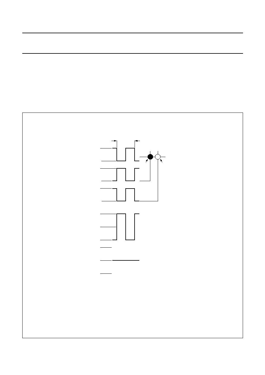
LCD drive mode waveforms
The static LCD drive mode is used when a single backplane is provided in the LCD. Backplane and segment drive
waveforms for this mode are shown in Fig.4.
When two backplanes are provided in the LCD the 1 : 2 multiplex drive mode applies. The OM4085 allows use of
1
/
2
or
1
/
3
bias in this mode as shown in Figs 5 and 6.
The backplane and segment drive waveforms for the 1 : 3 multiplex drive mode (three LCD backplanes) and for the 1 : 4
multiplex drive mode (four LCD backplanes) are shown in Figs 7 and 8 respectively.
Fig.4 Static drive mode waveforms: V
op
= V
DD
-
V
LCD
.
handbook, full pagewidth
MGG392
state 1
At any instant (t):
Vstate 1(t) = VSn(t)
-
VBP0(t)
Von(rms) = Vop
Vstate 2(t) = VSn
+
1
(t)
-
VBP0(t)
Voff(rms) = 0 V
0
BP0
state 2
0
(a) waveforms at driver
(b) resultant waveforms
at LCD segment
LCD segments
state 1
(on)
state 2
(off)
VDD
VLCD
VDD
VLCD
VDD
VLCD
Vop
-
Vop
Vop
-
Vop
Tframe
Sn
Sn
+
1
1997 Feb 25
8
Philips Semiconductors
Product specification
Universal LCD driver for low multiplex
rates
OM4085
Fig.5 Waveforms for 1 : 2 multiplex drive mode with
1
/
2
bias: V
op
= V
DD
-
V
LCD
.
handbook, full pagewidth
MGG394
state 1
BP0
Sn
+
1
(a) waveforms at driver
(b) resultant waveforms
at LCD segment
LCD segments
state 2
BP1
Sn
state 2
state 1
VDD
(VDD
+
VLCD)/2
VLCD
VDD
(VDD
+
VLCD)/2
VLCD
VDD
VLCD
VDD
VLCD
Vop
Vop/2
0
-
Vop/2
-
Vop
Vop
Vop/2
0
-
Vop/2
-
Vop
Tframe
At any instant (t):
Vstate 1(t) = VSn(t)
-
VBP0(t)
Von(rms) =
Vop
10 = 0.791Vop
4
Vstate 2(t) = VSn(t)
-
VBP1(t)
Voff(rms) =
Vop
2 = 0.354Vop
4
1997 Feb 25
9
Philips Semiconductors
Product specification
Universal LCD driver for low multiplex
rates
OM4085
Fig.6 Waveforms for 1 : 2 multiplex drive mode with
1
/
3
bias: V
op
= V
DD
-
V
LCD
.
handbook, full pagewidth
MGG393
state 1
0
BP0
(a) waveforms at driver
(b) resultant waveforms
at LCD segment
LCD segments
state 2
BP1
state 1
state 2
0
VDD
VDD
-
Vop/3
VDD
-
2Vop/3
VLCD
VDD
VDD
-
Vop/3
VDD
-
2Vop/3
VLCD
VDD
VDD
-
Vop/3
VDD
-
2Vop/3
VLCD
VDD
VDD
-
Vop/3
VDD
-
2Vop/3
VLCD
Vop
-
Vop
2Vop/3
-
2Vop/3
Vop/3
-
Vop/3
Vop
-
Vop
2Vop/3
-
2Vop/3
Vop/3
-
Vop/3
Sn
+
1
Sn
Tframe
At any instant (t):
Vstate 1(t) = VSn(t)
-
VBP0(t)
Von(rms) =
Vop
5 = 0.745Vop
3
Vstate 2(t) = VSn(t)
-
VBP1(t)
Voff(rms) =
Vop
= 0.333Vop
3
1997 Feb 25
10
Philips Semiconductors
Product specification
Universal LCD driver for low multiplex
rates
OM4085
Fig.7 Waveforms for 1 : 3 multiplex drive mode: V
op
= V
DD
-
V
LCD
.
handbook, full pagewidth
MGG395
state 1
0
BP0
(b) resultant waveforms
at LCD segment
LCD segments
state 2
BP1
state 1
state 2
0
(a) waveforms at driver
BP2
VDD
VDD
-
Vop/3
VDD
-
2Vop/3
VLCD
VDD
VDD
-
Vop/3
VDD
-
2Vop/3
VLCD
VDD
VDD
-
Vop/3
VDD
-
2Vop/3
VLCD
VDD
VDD
-
Vop/3
VDD
-
2Vop/3
VLCD
VDD
VDD
-
Vop/3
VDD
-
2Vop/3
VLCD
VDD
VDD
-
Vop/3
VDD
-
2Vop/3
VLCD
Vop
-
Vop
2Vop/3
-
2Vop/3
Vop/3
-
Vop/3
Vop
-
Vop
2Vop/3
-
2Vop/3
Vop/3
-
Vop/3
Sn
Sn
+
1
Sn
+
2
Tframe
At any instant (t):
Vstate 1(t) = VSn(t)
-
VBP0(t)
Von(rms) =
Vop
33 = 0.638Vop
9
Vstate 2(t) = VSn(t)
-
VBP1(t)
Voff(rms) =
Vop
= 0.333Vop
3

1997 Feb 25
11
Philips Semiconductors
Product specification
Universal LCD driver for low multiplex
rates
OM4085
Fig.8 Waveforms for 1 : 4 multiplex drive mode: V
op
= V
DD
-
V
LCD.
handbook, full pagewidth
MGG396
state 1
0
BP0
(b) resultant waveforms
at LCD segment
LCD segments
state 2
BP1
state 1
state 2
0
BP2
(a) waveforms at driver
BP3
VDD
VDD
-
Vop/3
VDD
-
2Vop/3
VLCD
VDD
VDD
-
Vop/3
VDD
-
2Vop/3
VLCD
VDD
VDD
-
Vop/3
VDD
-
2Vop/3
VLCD
VDD
VDD
-
Vop/3
VDD
-
2Vop/3
VLCD
VDD
VDD
-
Vop/3
VDD
-
2Vop/3
VLCD
VDD
VDD
-
Vop/3
VDD
-
2Vop/3
VLCD
VDD
VDD
-
Vop/3
VDD
-
2Vop/3
VLCD
VDD
VDD
-
Vop/3
VDD
-
2Vop/3
VLCD
Vop
-
Vop
2Vop/3
-
2Vop/3
Vop/3
-
Vop/3
Vop
-
Vop
2Vop/3
-
2Vop/3
Vop/3
-
Vop/3
Sn
Sn
+
1
Sn
+
2
Sn
+
3
Tframe
At any instant (t):
Vstate 1(t) = VSn(t)
-
VBP0(t)
Von(rms) =
Vop
3 = 0.577Vop
3
Vstate 2(t) = VSn(t)
-
VBP1(t)
Voff(rms) =
Vop
= 0.333Vop
3

1997 Feb 25
12
Philips Semiconductors
Product specification
Universal LCD driver for low multiplex
rates
OM4085
Oscillator
The internal logic and the LCD drive signals of the
OM4085 or PCF8576 are timed either by the built-in
oscillator or from an external clock.
The clock frequency (f
CLK
) determines the LCD frame
frequency and the maximum rate for data reception from
the I
2
C-bus. To allow I
2
C-bus transmissions at their
maximum data rate of 100 kHz, f
CLK
should be chosen to
be above 125 kHz.
A clock signal must always be supplied to the device;
removing the clock may freeze the LCD in a DC state.
Internal clock
When the internal oscillator is used, OSC (pin 6) should be
tied to V
SS
. In this case, the output from CLK (pin 4)
provides the clock signal for cascaded OM4085s and
PCF8576s in the system.
External clock
The condition for external clock is made by tying OSC
(pin 6) to V
DD
; CLK (pin 4) then becomes the external
clock input.
Timing
The timing of the OM4085 organizes the internal data flow
of the device. This includes the transfer of display data
from the display RAM to the display segment outputs.
In cascaded applications, the synchronization signal
SYNC maintains the correct timing relationship between
the OM4085s in the system. The timing also generates the
LCD frame frequency which it derives as an integer
multiple of the clock frequency (Table 3). The frame
frequency is set by MODE SET commands when internal
clock is used, or by the frequency applied to pin 4 when
external clock is used.
Table 3
LCD frame frequencies
The ratio between the clock frequency and the LCD frame
frequency depends on the mode in which the device is
operating. In the power saving mode the reduction ratio is
six times smaller; this allows the clock frequency to be
reduced by a factor of six. The reduced clock frequency
results in a significant reduction in power dissipation.
OM4085 MODE
f
frame
NOMINAL
f
frame
(Hz)
Normal mode
f
CLK
/2880
64
Power saving mode
f
CLK
/480
64
The lower clock frequency has the disadvantage of
increasing the response time when large amounts of
display data are transmitted on the I
2
C-bus. When a
device is unable to `digest' a display data byte before the
next one arrives, it holds the SCL line LOW until the first
display data byte is stored. This slows down the
transmission rate of the I
2
C-bus but no data loss occurs.
Display latch
The display latch holds the display data while the
corresponding multiplex signals are generated. There is a
one-to-one relationship between the data in the display
latch, the LCD segment outputs and one column of the
display RAM.
Shift register
The shift register serves to transfer display information
from the display RAM to the display latch while previous
data are displayed.
Segment outputs
The LCD drive section includes 24 segment outputs
S0 to S23 (pins 17 to 40) which should be connected
directly to the LCD. The segment output signals are
generated in accordance with the multiplexed backplane
signals and with the data resident in the display latch.
When less than 24 segment outputs are required the
unused segment outputs should be left open-circuit.
Backplane outputs
The LCD drive section includes four backplane outputs
BP0 to BP3 which should be connected directly to the
LCD. The backplane output signals are generated in
accordance with the selected LCD drive mode. If less than
four backplane outputs are required the unused outputs
can be left open. In the 1 : 3 multiplex drive mode BP3
carries the same signal as BP1, therefore these two
adjacent outputs can be tied together to give enhanced
drive capabilities. In the 1 : 2 multiplex drive mode
BP0 and BP2, BP1 and BP3 respectively carry the same
signals and may also be paired to increase the drive
capabilities. In the static drive mode the same signal is
carried by all four backplane outputs and they can be
connected in parallel for very high drive requirements.
Display RAM
The display RAM is a static 24
◊
4-bit RAM which stores
LCD data. A logic 1 in the RAM bit-map indicates the `on'
state of the corresponding LCD segment; similarly, a
logic 0 indicates the `off' state.

1997 Feb 25
13
Philips Semiconductors
Product specification
Universal LCD driver for low multiplex
rates
OM4085
There is a one-to-one correspondence between the RAM
addresses and the segment outputs, and between the
individual bits of a RAM word and the backplane outputs.
The first RAM column corresponds to the 24 segments
operated with respect to backplane BP0 (see Fig.9).
In multiplexed LCD applications the segment data of the
second, third and fourth column of the display RAM are
time-multiplexed with BP1, BP2 and BP3 respectively.
When display data are transmitted to the OM4085 the
display bytes received are stored in the display RAM
according to the selected LCD drive mode. To illustrate the
filling order, an example of a 7-segment numeric display
showing all drive modes is given in Fig.10; the RAM filling
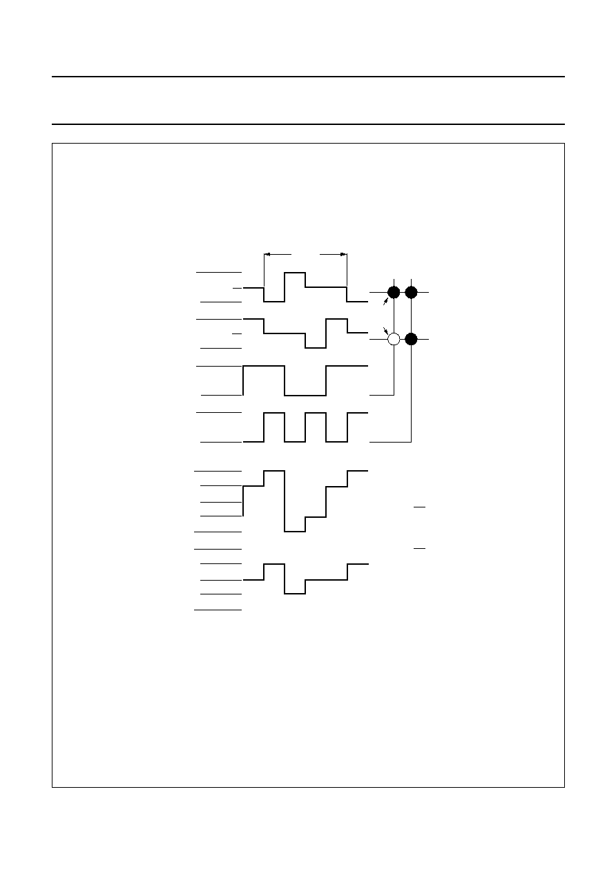
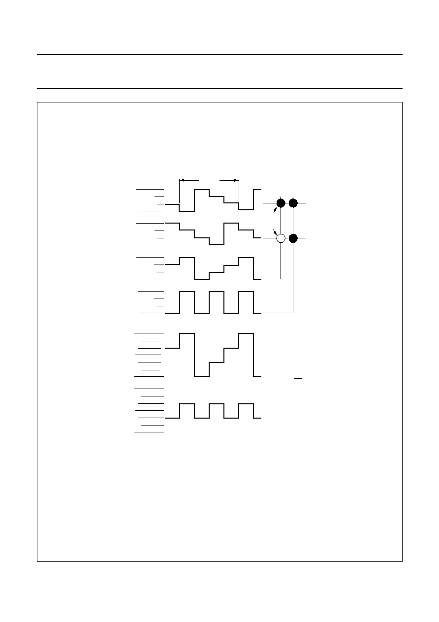
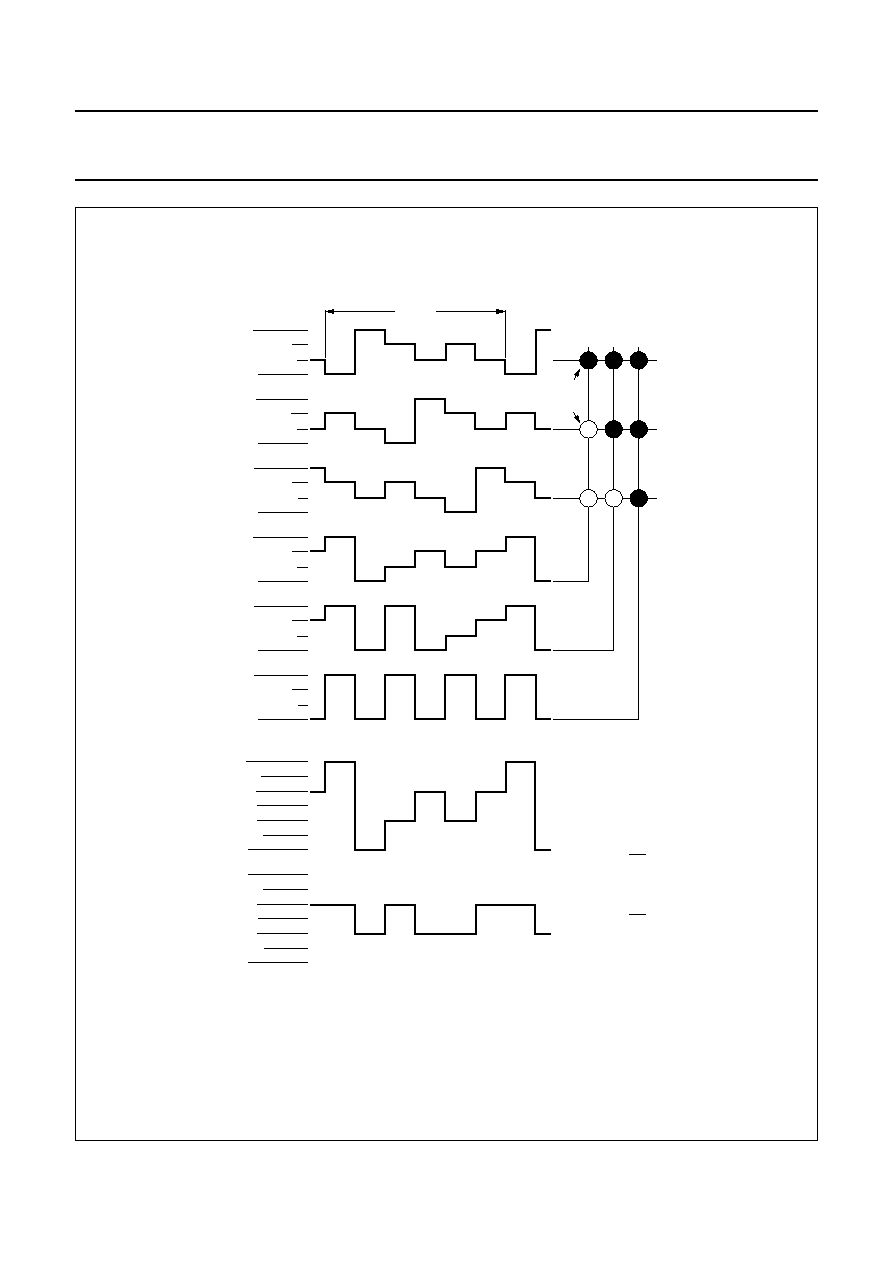
organization depicted applies equally to other LCD types.
With reference to Fig.10, in the static drive mode the eight
transmitted data bits are placed in bit 0 of eight successive
display RAM addresses. In the 1 : 2 multiplex drive mode
the eight transmitted data bits are placed in bits 0 and 1 of
four successive display RAM addresses. In the 1 : 3
multiplex drive mode these bits are placed in
bits 0, 1 and 2 of three successive addresses, with bit 2 of
the third address left unchanged. This last bit may, if
necessary, be controlled by an additional transfer to this
address but care should be taken to avoid overriding
adjacent data because full bytes are always transmitted.
In the 1 : 4 multiplex drive mode the eight transmitted data
bits are placed in bits 0, 1, 2 and 3 of two successive
display RAM addresses.
Data pointer
The addressing mechanism for the display RAM is
realized using the data pointer. This allows the loading of
an individual display data byte, or a series of display data
bytes, into any location of the display RAM.
The sequence commences with the initialization of the
data pointer by the LOAD DATA POINTER command.
Following this, an arriving data byte is stored starting at the
display RAM address indicated by the data pointer thereby
observing the filling order shown in Fig.10. The data
pointer is automatically incremented according to the LCD
configuration chosen. That is, after each byte is stored, the
contents of the data pointer are incremented by eight
(static drive mode), by four (1 : 2 multiplex drive mode), by
three (1 : 3 multiplex drive mode) or by two (1 : 4 multiplex
drive mode).
Subaddress counter
The storage of display data is conditioned by the contents
of the subaddress counter. Storage is allowed to take
place only when the contents of the subaddress counter
agree with the hardware subaddress applied to
A0, A1 and A2 (pins 7, 8, and 9). A0, A1 and A2 should
be tied to V
SS
or V
DD
. The subaddress counter value is
defined by the DEVICE SELECT command. If the contents
of the subaddress counter and the hardware subaddress
do not agree then data storage is inhibited but the data
pointer is incremented as if data storage had taken place.
The subaddress counter is also incremented when the
data pointer overflows.
The storage arrangements described lead to extremely
efficient data loading in cascaded applications. When a
series of display bytes are being sent to the display RAM,
automatic wrap-over to the next OM4085 occurs when the
last RAM address is exceeded. Subaddressing across
device boundaries is successful even if the change to the
next device in the cascade occurs within a transmitted
character.
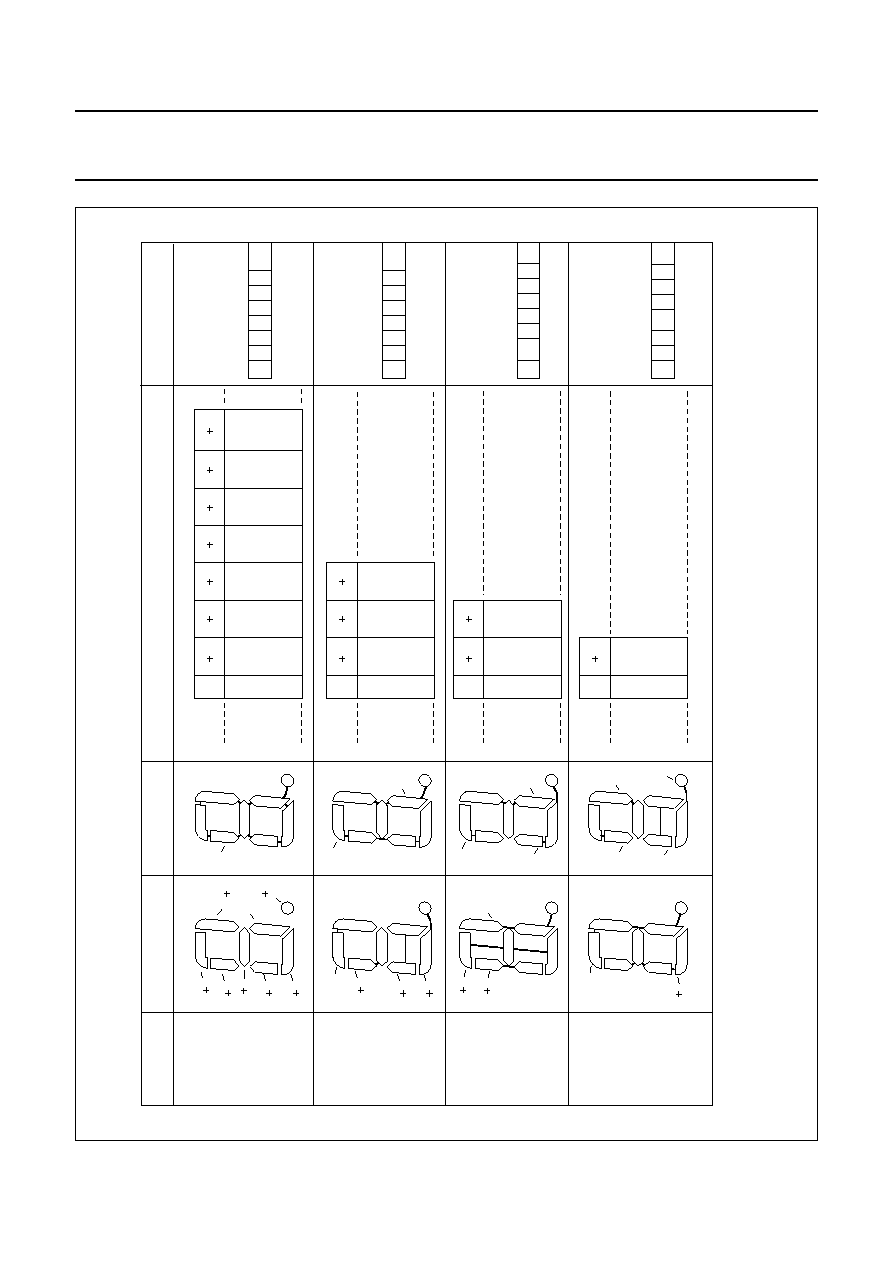
Fig.9
Display RAM bit-map showing direct relationship between display RAM addresses and segment outputs,
and between bits in a RAM word and backplane outputs.
handbook, full pagewidth
0
0
1
2
3
1
2
3
4
19
20
21
22
23
display RAM addresses (rows)/segment outputs (S)
display RAM bits
(columns) /
backplane outputs
(BP)
MGG389
1997
Feb
25
14
Philips Semiconductors
Product specification
Universal LCD driver for low multiplex
rates
OM4085
This text is here in white to force landscape pages to be rotated correctly when browsing through the pdf in the Acrobat reader.This text is here in
_
white to force landscape pages to be rotated correctly when browsing through the pdf in the Acrobat reader.This text is here inThis text is here in
white to force landscape pages to be rotated correctly when browsing through the pdf in the Acrobat reader. white to force landscape pages to be ...
handbook, full pagewidth
MBE534
S
2
n
S
1
n
S
7
n
S
n
S
n
S
3
n
S
5
n
S
2
n
S
3
n
S
1
n
S
1
n
S
1
n
S
2
n
S
n
S
6
n
S
n
S
4
n
DP
DP
DP
DP
a
f
b
g
e
c
d
a
f
b
g
e
c
d
a
f
b
g
e
c
d
a
f
b
g
e
c
d
BP0
BP0
BP0
BP1
BP1
BP2
BP1
BP2
BP3
BP0
n
c
x
x
x
0
1
2
3
b
x
x
x
a
x
x
x
f
x
x
x
g
x
x
x
e
x
x
x
d
x
x
x
DP
x
x
x
n 1
n 2
n 3
n 4
n 5
n 6
n 7
bit/
BP
n
a
b
x
x
0
1
2
3
f
g
x
x
e
c
x
x
d
DP
x
x
n 1
n 2
n 3
bit/
BP
n
b
DP
c
x
0
1
2
3
a
d
g
x
f
e
x
x
n 1
n 2
bit/
BP
n
a
c
b
DP
0
1
2
3
f
e
g
d
n 1
bit/
BP
c b a f
g e d DP
a b f
g e c d DP
b DP c a d g f
e
a c
b DP f
e g d
MSB
LSB
MSB
LSB
MSB
LSB
MSB
LSB
drive mode
static
1 : 2
multiplex
1 : 3
multiplex
1 : 4
multiplex
LCD segments
LCD backplanes
display RAM filling order
transmitted display byte
Fig.10 Relationships between LCD layout, drive mode, display RAM filling order and display data transmitted over the I
2
C-bus (X = data bit
unchanged).

1997 Feb 25
15
Philips Semiconductors
Product specification
Universal LCD driver for low multiplex
rates
OM4085
Output bank selector
This selects one of the four bits per display RAM address
for transfer to the display latch. The actual bit chosen
depends on the particular LCD drive mode in operation
and on the instant in the multiplex sequence. In 1 : 4
multiplex, all RAM addresses of bit 0 are the first to be
selected, these are followed by the contents of bit 1, bit 2
and then bit 3. Similarly in 1 : 3 multiplex, bits 0, 1 and 2
are selected sequentially. In 1 : 2 multiplex, bits 0 then 1
are selected and, in the static mode, bit 0 is selected.
The OM4085 includes a RAM bank switching feature in the
static and 1 : 2 multiplex drive modes. In the static drive
mode, the BANK SELECT command may request the
contents of bit 2 to be selected for display instead of bit 0
contents. In the 1 : 2 drive mode, the contents of
bits 2 and 3 may be selected instead of bits 0 and 1.
This gives the provision for preparing display information
in an alternative bank and to be able to switch to it once it
is assembled.
Input bank selector
The input bank selector loads display data into the display
RAM according to the selected LCD drive configuration.
Display data can be loaded in bit 2 in static drive mode or
in bits 2 and 3 in 1 : 2 drive mode by using the BANK
SELECT command. The input bank selector functions
independently of the output bank selector.
Blinker
The display blinking capabilities of the OM4085 are very
versatile. The whole display can be blinked at frequencies
selected by the BLINK command. The blinking frequencies
are integer multiples of the clock frequency; the ratios
between the clock and blinking frequencies depend on the
mode in which the device is operating, as shown in
Table 4.
An additional feature is for an arbitrary selection of LCD
segments to be blinked. This applies to the static and 1 : 2
LCD drive modes and can be implemented without any
communication overheads. By means of the output bank
selector, the displayed RAM banks are exchanged with
alternate RAM banks at the blinking frequency. This mode
can also be specified by the BLINK command.
In the 1 : 3 and 1 : 4 multiplex modes, where no alternate
RAM bank is available, groups of LCD segments can be
blinked by selectively changing the display RAM data at
fixed time intervals.
If the entire display is to be blinked at a frequency other
than the nominal blinking frequency, this can be effectively
performed by resetting and setting the display enable bit E
at the required rate using the MODE SET command.
Table 4
Blinking frequencies
BLINKING MODE
NORMAL OPERATING
MODE RATIO
POWER-SAVING
MODE RATIO
NOMINAL BLINKING FREQUENCY
f
blink
(Hz)
Off
-
-
blinking off
2 Hz
f
CLK
/92160
f
CLK
/15360
2
1 Hz
f
CLK
/184320
f
CLK
/30720
1
0.5 Hz
f
CLK
/368640
f
CLK
/61440
0.5
1997 Feb 25
16
Philips Semiconductors
Product specification
Universal LCD driver for low multiplex
rates
OM4085
I
2
C-BUS DESCRIPTION
The I
2
C-bus is for 2-way, 2-line communication between
different ICs or modules. The two lines are a serial data
line (SDA) and a serial clock line (SCL). Both lines must be
connected to a positive supply via a pull-up resistor when
connected to the output stages of a device. Data transfer
may be initiated only when the bus is not busy.
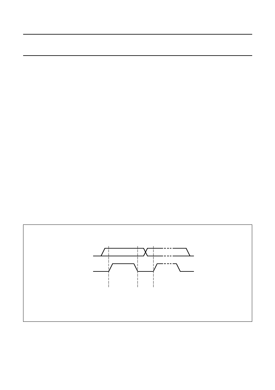
Bit transfer
One data bit is transferred during each clock pulse.
The data on the SDA line must remain stable during the
HIGH period of the clock pulse as changes in the data line
at this time will be interpreted as control signals.
Start and stop conditions
Both data and clock lines remain HIGH when the bus is not
busy. A HIGH-to-LOW transition of the data line while the
clock is HIGH is defined as the START condition (S).
A LOW-to-HIGH transition of the data line while the clock
is HIGH is defined as the STOP condition (P).
System configuration
A device generating a message is a `transmitter', a device
receiving a message is a `receiver'. The device that
controls the message is the `master' and the devices which
are controlled by the master are the `slaves'.
Acknowledge
The number of data bytes transferred between the START
and STOP conditions from transmitter to receiver is not
limited. Each byte is followed by one acknowledge bit.
The acknowledge bit is a HIGH level put on the bus by the
transmitter whereas the master generates an extra
acknowledge related clock pulse. A slave receiver which is
addressed must generate an acknowledge after the
reception of each byte. Also a master must generate an
acknowledge after the reception of each byte that has
been clocked out of the slave transmitter. The device that
acknowledges has to pull down the SDA line during the
acknowledge clock pulse, so that the SDA line is stable
LOW during the HIGH period of the acknowledge related
clock pulse, set up and hold times must be taken into
account. A master receiver must signal an end of data to
the transmitter by not generating an acknowledge on the
last byte that has been clocked out of the slave. In this
event the transmitter must leave the data line HIGH to
enable the master to generate a STOP condition.
Fig.11 Bit transfer.
MBA607
data line
stable;
data valid
change
of data
allowed
SDA
SCL

1997 Feb 25
17
Philips Semiconductors
Product specification
Universal LCD driver for low multiplex
rates
OM4085
Fig.12 Definition of START and STOP conditions.
MBA608
SDA
SCL
P
STOP condition
SDA
SCL
S
START condition
Fig.13 System configuration.
MBA605
MASTER
TRANSMITTER /
RECEIVER
SLAVE
RECEIVER
SLAVE
TRANSMITTER /
RECEIVER
MASTER
TRANSMITTER
MASTER
TRANSMITTER /
RECEIVER
SDA
SCL
Fig.14 Acknowledgement on the I
2
C-bus.
handbook, full pagewidth
MBA606 - 1
START
condition
S
SCL FROM
MASTER
DATA OUTPUT
BY TRANSMITTER
DATA OUTPUT
BY RECEIVER
clock pulse for
acknowledgement
1
2
8
9

1997 Feb 25
18
Philips Semiconductors
Product specification
Universal LCD driver for low multiplex
rates
OM4085
OM4085 I
2
C-bus controller
The OM4085 acts as an I
2
C-bus slave receiver. It does not
initiate I
2
C-bus transfers or transmit data to an I
2
C-bus
master receiver. The only data output from the OM4085
are the acknowledge signals of the selected devices.
Device selection depends on the I
2
C-bus slave address,
on the transferred command data and on the hardware
subaddress.
In single device applications, the hardware subaddress
inputs A0, A1 and A2 are normally left open-circuit or tied
to V
SS
which defines the hardware subaddress 0.
In multiple device applications A0, A1 and A2 are left
open-circuit or tied to V
SS
or V
DD
according to a binary
coding scheme such that no two devices with a common
I
2
C-bus slave address have the same hardware
subaddress.
In the power-saving mode it is possible that the OM4085 is
not able to keep up with the highest transmission rates
when large amounts of display data are transmitted. If this
situation occurs, the OM4085 forces the SCL line LOW
until its internal operations are completed. This is known
as the `clock synchronization feature' of the I
2
C-bus and
serves to slow down fast transmitters. Data loss does not
occur.
Input filters
To enhance noise immunity in electrically adverse
environments, RC low-pass filters are provided on the
SDA and SCL lines.
I
2
C-bus protocol
Two I
2
C-bus slave addresses (0111110 and 0111111) are
reserved for OM4085. The least-significant bit of the slave
address that a OM4085 will respond to is defined by the
level tied at its input SA0 (pin 10). Therefore, two types of
OM4085 can be distinguished on the same I
2
C-bus which
allows:
1. Up to 16 OM4085s on the same I
2
C-bus for very large
LCD applications
2. The use of two types of LCD multiplex on the same
I
2
C-bus.
The I
2
C-bus protocol is shown in Fig.15. The sequence is
initiated with a START condition (S) from the I
2
C-bus
master which is followed by one of the two OM4085 slave
addresses available. All OM4085s with the corresponding
SA0 level acknowledge in parallel the slave address but all
OM4085s with the alternative SA0 level ignore the whole
I
2
C-bus transfer. After acknowledgement, one or more
command bytes (m) follow which define the status of the
addressed OM4085s. The last command byte is tagged
with a cleared most-significant bit, the continuation bit C.
The command bytes are also acknowledged by all
addressed OM4085s on the bus.
After the last command byte, a series of display data bytes
(n) may follow. These display data bytes are stored in the
display RAM at the address specified by the data pointer
and the subaddress counter. Both data pointer and
subaddress counter are automatically updated and the
data are directed to the intended OM4085 device.
The acknowledgement after each byte is made only by the
(A0, A1, A2) addressed OM4085. After the last display
byte, the I
2
C-bus master issues a STOP condition (P).
Command decoder
The command decoder identifies command bytes that
arrive on the I
2
C-bus. All available commands carry a
continuation bit C in their most-significant bit position
(see Fig.16). When this bit is set, it indicates that the next
byte of the transfer to arrive will also represent a
command.
If the bit is reset, it indicates the last command byte of the
transfer. Further bytes will be regarded as display data.
The five commands available to the OM4085 are defined
in Table 5.
1997 Feb 25
19
Philips Semiconductors
Product specification
Universal LCD driver for low multiplex
rates
OM4085
Fig.15 I
2
C-bus protocol.
handbook, full pagewidth
MBH953
S
A
0
S
0 1 1 1 1 1
0 A C
COMMAND
A
P
A
DISPLAY DATA
slave address
/
R W
acknowledge by
all addressed
OM4085s
acknowledge
by A0, A1 and A2
selected
OM4085 only
m
1 byte(s)
n
0
byte(s)
1 byte
update data pointers
and if necessary,
subaddress counter
Fig.16 General format of command byte.
MGG388
REST OF OPCODE
C
MSB
LSB
0 = last command
1 = commands continue
1997 Feb 25
20
Philips Semiconductors
Product specification
Universal LCD driver for low multiplex
rates
OM4085
Table 5
Definition of OM4085 commands
Table 6
LCD drive mode
COMMAND/OPCODE
OPTIONS
DESCRIPTION
Mode set
C
1
0
LP
E
B
M1
M0
see Table 6
defines LCD drive mode
see Table 7
defines LCD bias configuration
see Table 8
defines display status; the possibility to disable
the display allows implementation of blinking
under external control
see Table 9
defines power dissipation mode
Load data pointer
C
0
0
P4
P3
P2
P1
P0
see Table 10
five bits of immediate data, bits P4 to P0, are
transferred to the data pointer to define one of
twenty-four display RAM addresses
Device select
C
1
1
0
0
A2
A1
A0
see Table 11
three bits of immediate data, bits A0 to A2, are
transferred to the subaddress counter to define
one of eight hardware subaddresses
Bank select
C
1
1
1
1
0
I
O
see Table 12
defines input bank selection (storage of arriving
display data)
see Table 13
defines output bank selection (retrieval of LCD
display data)
the BANK SELECT command has no effect in
1 : 3 and 1 : 4 multiplex drive modes
Blink
C
1
1
1
0
A
BF1 BF0
see Table 14
defines the blinking frequency
see Table 15
selects the blinking mode; normal operation
with frequency set by bits BF1 and BF0, or
blinking by alternation of display RAM banks.
Alternation blinking does not apply in 1 : 3 and
1 : 4 multiplex drive modes
LCD DRIVE MODE
BIT M1
BIT M0
Static (1 BP)
0
1
1 : 2 MUX (2 BP)
1
0
1 : 3 MUX (3 BP)
1
1
1 : 4 MUX (4 BP)
0
0
1997 Feb 25
21
Philips Semiconductors
Product specification
Universal LCD driver for low multiplex
rates
OM4085
Table 7
LCD bias configuration
Table 8
Display status
Table 9
Power dissipation mode
Table 10 Load data pointer
Table 11 Device select
Table 12 Input bank selection
Table 13 Output bank selection
Table 14 Blinking frequency
LCD BIAS
BIT B
1
/
3
bias
0
1
/
2
bias
1
DISPLAY STATUS
BIT E
Disabled (blank)
0
Enabled
1
MODE
BIT LP
Normal mode
0
Power-saving mode
1
BITS
P4
P3
P2
P1
P0
5-bit binary value of 0 to 23
BITS
A0
A1
A2
3-bit binary value of 0 to 7
STATIC
1 : 2 MUX
BIT 1
RAM bit 0
RAM bits 0, 1
0
RAM bit 2
RAM bits 2, 3
1
STATIC
1 : 2 MUX
BIT 0
RAM bit 0
RAM bits 0, 1
0
RAM bit 2
RAM bits 2, 3
1
BLINK
FREQUENCY
BIT BF1
BIT BF0
Off
0
0
2 Hz
0
1
1 Hz
1
0
0.5 Hz
1
1
Table 15 Blink mode selection
Display controller
The display controller executes the commands identified
by the command decoder. It contains the status registers
of the OM4085 and coordinates their effects.
The controller is also responsible for loading display data
into the display RAM as required by the filling order.
Cascaded operation
In large display configurations, up to 16 OM4085s can be
distinguished on the same I
2
C-bus by using the 3-bit
hardware subaddress (A0, A1 and A2) and the
programmable I
2
C-bus slave address (SA0). It is also
possible to cascade up to 16 OM4085s. When cascaded,
several OM4085s are synchronized so that they can share
the backplane signals from one of the devices in the
cascade. Such an arrangement is cost-effective in large
LCD applications since the outputs of only one device
need to be through-plated to the backplane electrodes of
the display. The other OM4085s of the cascade contribute
additional segment outputs but their backplane outputs are
left open-circuit (Fig.17).
The SYNC line is provided to maintain the correct
synchronization between all cascaded OM4085s.
This synchronization is guaranteed after the power-on
reset. The only time that SYNC is likely to be needed is if
synchronization is accidentally lost (e.g. by noise in
adverse electrical environments; or by the definition of a
multiplex mode when OM4085s with differing SA0 levels
are cascaded). SYNC is organized as an input/output pin;
the output section being realized as an open-drain driver
with an internal pull-up resistor. A OM4085 asserts the
SYNC line at the onset of its last active backplane signal
and monitors the SYNC line at all other times.
Should synchronization in the cascade be lost, it will be
restored by the first OM4085 to assert SYNC. The timing
relationships between the backplane waveforms and the
SYNC signal for the various drive modes of the PCF8576
are shown in Fig.18. The waveforms are identical with the
parent device PCF8576. Cascade ability between
OM4085s and PCF8576s is possible, giving cost effective
LCD applications.
BLINK MODE
BIT A
Normal blinking
0
Alternation blinking
1

1997 Feb 25
22
Philips Semiconductors
Product specification
Universal LCD driver for low multiplex
rates
OM4085
Fig.17 Cascaded OM4085 configuration.
handbook, full pagewidth
HOST
MICRO-
PROCESSOR/
MICRO-
CONTROLLER
SDA
SCL
CLK
OSC
SYNC
1
17 to 40
13 to 16
13 to 16
2
3
4
6
7
8
5
12
9
10
11
7
8
9
10
11
24 segment drives
4 backplanes
24 segment drives
LCD PANEL
(up to 1536
elements)
OM4085
OM4085
A0
A1
A2
SA0
MBH950
SDA
SCL
SYNC
CLK
OSC
1
5
12
2
3
4
6
17 to 40
BP0 to BP3
(open-circuit)
A0
A1
A2
SA0
BP0 to BP3
VDD
VLCD
VSS
VDD
VLCD
VSS
VLCD
VDD
VSS
R
trise
2 Cbus

1997 Feb 25
23
Philips Semiconductors
Product specification
Universal LCD driver for low multiplex
rates
OM4085
For single plane wiring of OM4085s, see Chapter "Application information".
Fig.18 Synchronization of the cascade for the various OM4085 drive modes.
handbook, full pagewidth
T
=
frame
f
frame
1
BP0
SYNC
BP1
(1/2 bias)
SYNC
BP2
(a) static drive mode.
(b) 1 : 2 multiplex drive mode.
(c) 1 : 3 multiplex drive mode.
(d) 1 : 4 multiplex drive mode.
BP3
SYNC
SYNC
BP1
(1/3 bias)
MBE535

1997 Feb 25
24
Philips Semiconductors
Product specification
Universal LCD driver for low multiplex
rates
OM4085
LIMITING VALUES
In accordance with the Absolute Maximum Rating System (IEC 134).
HANDLING
Inputs and outputs are protected against electrostatic discharges in normal handling. However, to be totally safe, it is
advised to take handling precautions appropriate to handling MOS devices (see
"Handling MOS devices").
SYMBOL
PARAMETER
MIN.
MAX.
UNIT
V
DD
supply voltage
-
0.5
+7
V
V
LCD
LCD supply voltage
V
DD
-
7
V
DD
V
V
I
input voltage (SCL, SDA, A0 to A2, OSC, CLK, SYNC and SA0)
V
SS
-
0.5
V
DD
+ 0.5
V
V
O
output voltage (S0 to S23 and BP0 to BP3)
V
LCD
-
0.5
V
DD
+ 0.5
V
I
I
DC input current
-
±
20
mA
I
O
DC output current
-
±
25
mA
I
DD
, I
SS
, I
LCD
V
DD
, V
SS
or V
LCD
current
-
±
50
mA
P
tot
power dissipation per package
-
400
mW
P
O
power dissipation per output
-
100
mW
T
stg
storage temperature
-
65
+150
∞
C

1997 Feb 25
25
Philips Semiconductors
Product specification
Universal LCD driver for low multiplex
rates
OM4085
DC CHARACTERISTICS
V
SS
= 0 V; V
DD
= 2.0 to 6 V; V
LCD
= V
DD
-
2.0 to V
DD
-
6 V; T
amb
=
-
40 to +85
∞
C; unless otherwise specified.
Notes
1. Outputs open; inputs at V
SS
or V
DD
; external clock with 50% duty factor; I
2
C-bus inactive.
2. Resets all logic when V
DD
< V
ref
.
3. Periodically sampled, not 100% tested.
4. Outputs measured one at a time.
SYMBOL
PARAMETER
CONDITIONS
MIN.
TYP.
MAX.
UNIT
Supplies
V
DD
operating supply voltage
2.0
-
6
V
V
LCD
LCD supply voltage
V
DD
-
6
-
V
DD
-
2.0 V
I
DD
operating supply current
(normal mode)
f
CLK
= 200 kHz; note 1
-
30
90
µ
A
I
LP
power saving mode supply current
V
DD
= 3.5 V; V
LCD
= 0 V;
f
CLK
= 35 kHz; A0,
A1 and A2 tied to V
SS
;
note 1
-
15
40
µ
A
Logic
V
IL
LOW level input voltage
V
SS
-
0.3V
DD
V
V
IH
HIGH level input voltage
0.7V
DD
-
V
DD
V
V
OL
LOW level output voltage
I
O
= 0 mA
-
-
0.05
V
V
OH
HIGH level output voltage
I
O
= 0 mA
V
DD
-
0.05
-
-
V
I
OL1
LOW level output current
(CLK and SYNC)
V
OL
= 1 V; V
DD
= 5 V
1
-
-
mA
I
OH
HIGH level output current (CLK)
V
OH
= 4 V; V
DD
= 5 V
-
-
-
1
mA
I
OL2
LOW level output current
(SDA and SCL)
V
OL
= 0.4 V; V
DD
= 5 V
3
-
-
mA
I
LI
leakage current
(SA0, CLK, OSC, A0, A1, A2, SCL
and SDA)
V
I
= V
SS
or V
DD
-
-
±
1
µ
A
I
pd
pull-down current
(A0, A1, A2 and OSC)
V
I
= 1 V; V
DD
= 5 V
15
50
150
µ
A
R
puSYNC
pull-up resistor (SYNC)
15
25
60
k
V
ref
power-on reset level
note 2
-
1.3
2
V
t
sw
tolerable spike width on bus
-
-
100
ns
C
i
input capacitance
note 3
-
-
7
pF
LCD outputs
V
BP
DC voltage component
(BP0 to BP3)
C
BP
= 35 nF
-
±
20
-
mV
V
S
DC voltage component (S0 to S23)
C
S
= 5 nF
-
±
20
-
mV
Z
BP
output impedance (BP0 to BP3)
V
LCD
= V
DD
-
5 V; note 4
-
1
5
k
Z
S
output impedance (S0 to S23)
V
LCD
= V
DD
-
5 V; note 4
-
3
7
k
1997 Feb 25
26
Philips Semiconductors
Product specification
Universal LCD driver for low multiplex
rates
OM4085
AC CHARACTERISTICS
V
SS
= 0 V; V
DD
= 2.0 to 6 V; V
LCD
= V
DD
-
2.0 to V
DD
-
6 V; T
amb
=
-
40 to +85
∞
C; unless otherwise specified; note 1.
Notes
1. All timing values referred to V
IH
and V
IL
levels with an input voltage swing of V
SS
to V
DD
.
2. At f
CLK
< 125 kHz, I
2
C-bus maximum transmission speed is derated.
SYMBOL
PARAMETER
CONDITIONS
MIN.
TYP.
MAX.
UNIT
f
CLK
oscillator frequency (normal mode)
V
DD
= 5 V; note 2
125
200
315
kHz
f
CLKLP
oscillator frequency (power saving
mode)
V
DD
= 3.5 V
21
31
48
kHz
t
CLKH
CLK HIGH time
1
-
-
µ
s
t
CLKL
CLK LOW time
1
-
-
µ
s
t
PSYNC
SYNC propagation delay
-
-
400
ns
t
SYNCL
SYNC LOW time
1
-
-
µ
s
t
PLCD
driver delays with test loads
V
LCD
= V
DD
-
5 V
-
-
30
µ
s
I
2
C-bus
t
BUF
bus free time
4.7
-
-
µ
s
t
HD; STA
START condition hold time
4
-
-
µ
s
t
LOW
SCL LOW time
4.7
-
-
µ
s
t
HIGH
SCL HIGH time
4
-
-
µ
s
t
SU; STA
START condition set-up time
(repeated start code only)
4.7
-
-
µ
s
t
HD; DAT
data hold time
0
-
-
µ
s
t
SU; DAT
data set-up time
250
-
-
ns
t
r
rise time
-
-
1
µ
s
t
f
fall time
-
-
300
ns
t
SU; STO
STOP condition set-up time
4.7
-
-
µ
s
Fig.19 Test loads.
handbook, full pagewidth
MGG387
3.3 k
1.5 k
6.8 k
(2%)
(2%)
(2%)
CLK
(pin 4)
SDA, SCL
(pins 1, 2)
SYNC
(pin 3)
0.5VDD
VDD
VDD
S0 to S23
(pins 17 to 40)
Iload
15
µ
A
Iload
25
µ
A
BP0 to BP3
(pins 13 to 16)

1997 Feb 25
27
Philips Semiconductors
Product specification
Universal LCD driver for low multiplex
rates
OM4085
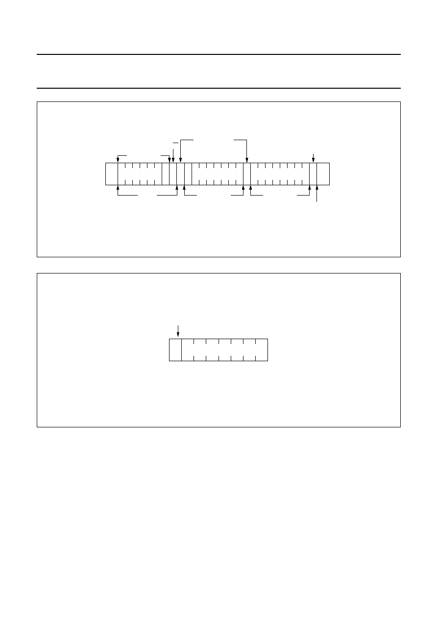
Fig.20 Driver timing waveforms.
handbook, full pagewidth
MGG391
1
fCLK
tCLKH
tCLKL
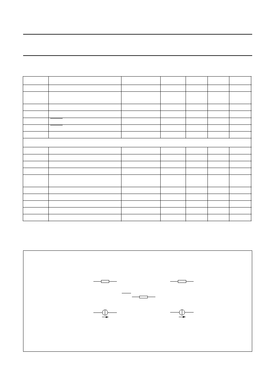
tPSYNC
tSYNCL
tPLCD
0.5 V
0.5 V
(VDD = 5 V)
0.3VDD
0.7VDD
0.3VDD
0.7VDD
CLK
SYNC
BP0 to BP3
S0 to S23
Fig.21 I
2
C-bus timing waveforms.
handbook, full pagewidth
SDA
MGA728
SDA
SCL
t SU;STA
t
SU;STO
t
HD;STA
t BUF
t LOW
t HD;DAT
t HIGH
t r
t f
t SU;DAT
1997 Feb 25
28
Philips Semiconductors
Product specification
Universal LCD driver for low multiplex
rates
OM4085
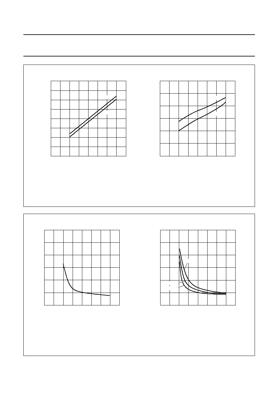
Fig.22 Typical supply current characteristics.
a. Normal mode; V
LCD
= 0 V;
external clock = 200 kHz.
b. Low power mode; V
LCD
= 0 V;
external clock = 35 kHz.
handbook, halfpage
40
30
10
20
MGG397
0
0
2
4
8
6
VDD (V)
IDD
(
µ
A)
+
85
∞
C
-
40
∞
C
handbook, halfpage
0
24
16
8
0
2
4
8
6
MGG398
VDD (V)
IDD
(
µ
A)
-
40
∞
C
+
85
∞
C
Fig.23 Typical characteristics of LCD outputs.
a. Backplane output impedance BP0 to BP3
(R
BP
); V
DD
= 5 V; T
amb
=
-
40 to +85
∞
C.
b. Segment output impedance S0 to S23 (R
S
);
V
DD
= 5 V.
handbook, halfpage
0
6
4
2
0
2
4
8
6
MGG399
VDD (V)
RBP
(k
)
handbook, halfpage
0
12
8
4
0
2
4
8
6
MGG400
VDD (V)
RS
(k
)
+
25
∞
C
+
85
∞
C
-
40
∞
C

1997
Feb
25
29
Philips Semiconductors
Product specification
Universal LCD driver for low multiplex
rates
OM4085
This text is here in white to force landscape pages to be rotated correctly when browsing through the pdf in the Acrobat reader.This text is here in
_
white to force landscape pages to be rotated correctly when browsing through the pdf in the Acrobat reader.This text is here inThis text is here in
white to force landscape pages to be rotated correctly when browsing through the pdf in the Acrobat reader. white to force landscape pages to be ...
APPLICA
TION INFORMA
TION
Fig.24 Single plane wiring of package OM4085s.
handbook, full pagewidth
MBH952
OM4085
1
2
3
4
5
6
7
8
9
10
11
12
13
14
15
16
17
18
19
20
40
39
38
37
36
35
34
33
32
31
30
29
28
27
26
25
24
23
22
21
S23
S23
S22
S21
S20
S19
S18
S17
S16
S15
S14
S13
S12
S11
S10
S9
S8
S7
S6
S5
S4
SDA
SCL
SYNC
CLK
VDD
OSC
A0
A1
A2
SA0
VSS
VLCD
VSS
VLCD
BP0
BP2
BP1
BP3
S0
S0
S1
S2
S3
SDA
SCL
SYNC
CLK
VDD
OM4085
1
2
3
4
5
6
7
8
9
10
11
12
13
14
15
16
17
18
19
20
40
39
38
37
36
35
34
33
32
31
30
29
28
27
26
25
24
23
22
21
S47
S47
S46
S45
S44
S43
S42
S41
S40
S39
S38
S37
S36
S35
S34
S33
S32
S31
S30
S29
S28
BP0
BP2
BP1
BP3
S24
S24
S25
S26
S27
open-circuit
BACKPLANES
SEGMENTS
1997 Feb 25
30
Philips Semiconductors
Product specification
Universal LCD driver for low multiplex
rates
OM4085
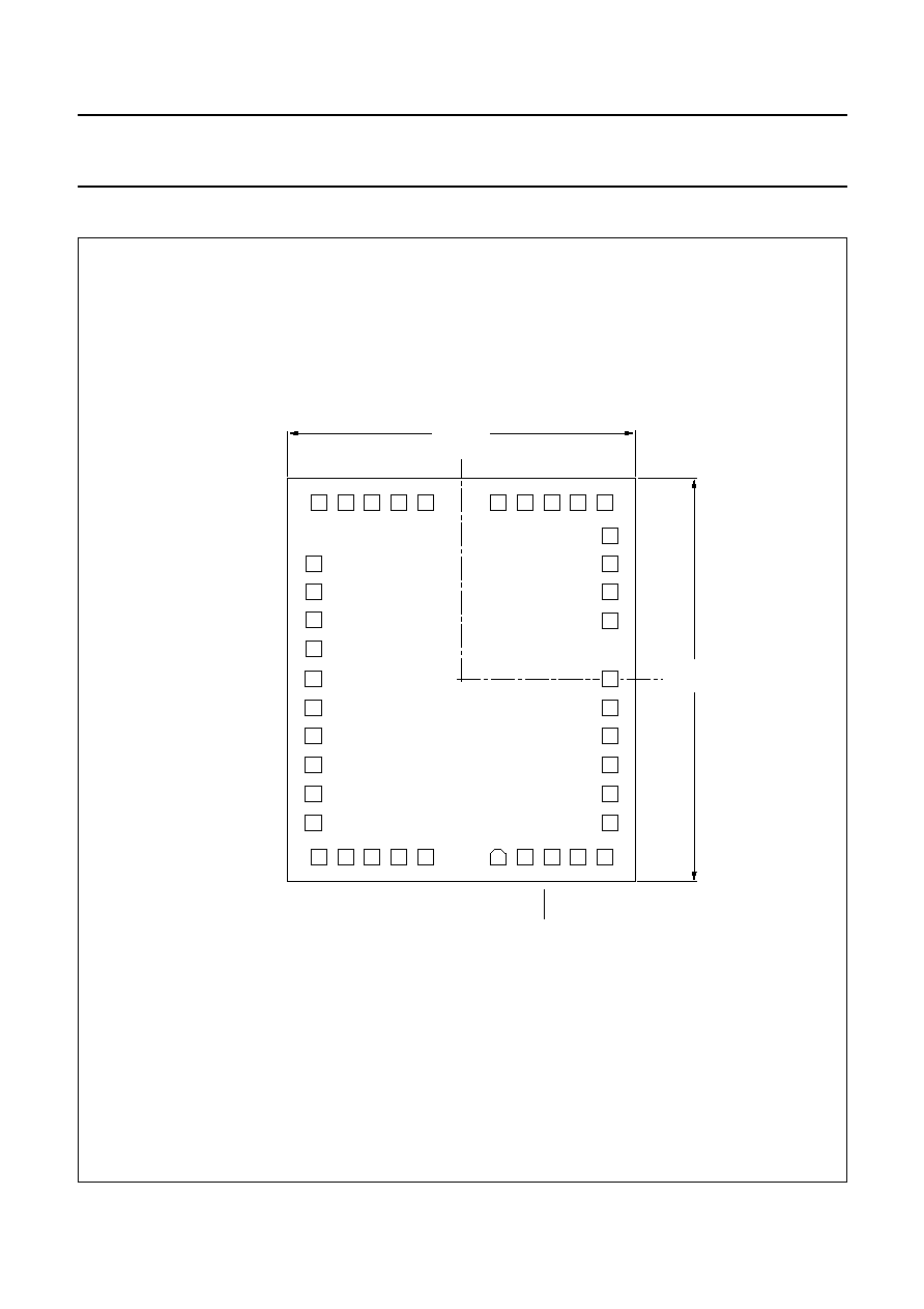
CHIP DIMENSIONS AND BONDING PAD LOCATIONS
Fig.25 Bonding pad locations.
(1) Typical value.
Pad size: 120
◊
120
µ
m
Chip area: 7.27 mm.
The numbers given in the small squares refer to the pad numbers.
handbook, full pagewidth
MBH949
y
2.5 mm
(1)
x
0
0
OM4085
36
37
38
39
40
5
4
3
2
1
25
24
23
22
21
16
15
14
2.91
(1)
mm
13
12
11
10
17
18
19
20
9
8
7
6
30
31
32
33
34
35
26
27
28
29
S23
S22
S21
S20
S19
V
DD
CLK
SYNC
SCL
SDA
S5
S7
S8
S6
SA0
A2
A1
A0
OSC
S16
S17
S18
VSS
VLCD
BP0
BP2
BP1
S11
S10
S9
S12
S14
S13
S15
BP3
S0
S1
S2
S3
S4

1997 Feb 25
31
Philips Semiconductors
Product specification
Universal LCD driver for low multiplex
rates
OM4085
Table 16 Bonding pad locations (dimensions in mm)
All x/y coordinates are referenced to centre of chip, (see Fig.25)
PAD NUMBER
SYMBOL
x
y
PIN
1
SDA
200
-
1235
1
2
SCL
400
-
1235
2
3
SYNC
605
-
1235
3
4
CLK
856
-
1235
4
5
V
DD
1062
-
1235
5
6
OSC
1080
-
1025
6
7
A0
1080
-
825
7
8
A1
1080
-
625
8
9
A2
1080
-
425
9
10
SA0
1080
-
225
10
11
V
SS
1080
-
25
11
12
V
LCD
1080
347
12
13
BP0
1080
547
13
14
BP2
1080
747
14
15
BP1
1080
947
15
16
BP3
1074
1235
16
17
S0
674
1235
17
18
S1
674
1235
18
19
S2
474
1235
19
20
S3
274
1235
20
21
S4
-
274
1235
21
22
S5
-
474
1235
22
23
S6
-
674
1235
23
24
S7
-
874
1235
24
25
S8
-
1074
1235
25
26
S9
-
1080
765
26
27
S10
-
1080
565
27
28
S11
-
1080
365
28
29
S12
-
1080
165
29
30
S13
-
1080
-
35
30
31
S14
-
1080
-
235
31
32
S15
-
1080
-
435
32
33
S16
-
1080
-
635
33
34
S17
-
1080
-
835
34
35
S18
-
1080
-
1035
35
36
S19
-
1056
-
1235
36
37
S20
-
830
-
1235
37
38
S21
-
630
-
1235
38
39
S22
-
430
-
1235
39
40
S23
-
230
-
1235
40
1997 Feb 25
32
Philips Semiconductors
Product specification
Universal LCD driver for low multiplex
rates
OM4085
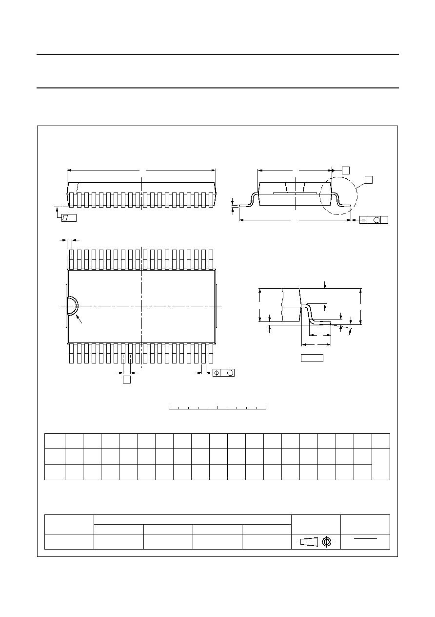
PACKAGE OUTLINE
UNIT
A
1
A
2
A
3
b
p
c
D
(1)
E
(2)
Z
(1)
e
H
E
L
L
p
Q
y
w
v
REFERENCES
OUTLINE
VERSION
EUROPEAN
PROJECTION
ISSUE DATE
IEC
JEDEC
EIAJ
mm
inches
0.3
0.1
2.45
2.25
0.25
0.42
0.30
0.22
0.14
15.6
15.2
7.6
7.5
0.762
2.25
12.3
11.8
1.15
1.05
0.6
0.3
7
0
o
o
0.1
0.1
DIMENSIONS (inch dimensions are derived from the original mm dimensions)
Notes
1. Plastic or metal protrusions of 0.4 mm maximum per side are not included.
2. Plastic interlead protrusions of 0.25 mm maximum per side are not included.
1.7
1.5
SOT158-1
92-11-17
95-01-24
X
w
M
A
A
1
A
2
b
p
D
H
E
L
p
Q
detail X
E
Z
e
c
L
v
M
A
(A )
3
A
y
40
20
21
1
pin 1 index
0.012
0.004
0.096
0.089
0.017
0.012
0.0087
0.0055
0.61
0.60
0.30
0.29
0.03
0.089
0.48
0.46
0.045
0.041
0.024
0.012
0.004
0.2
0.008
0.004
0.067
0.059
0.010
0
5
10 mm
scale
VSO40: plastic very small outline package; 40 leads
SOT158-1
A
max.
2.70
0.11

1997 Feb 25
33
Philips Semiconductors
Product specification
Universal LCD driver for low multiplex
rates
OM4085
SOLDERING
Introduction
There is no soldering method that is ideal for all IC
packages. Wave soldering is often preferred when
through-hole and surface mounted components are mixed
on one printed-circuit board. However, wave soldering is
not always suitable for surface mounted ICs, or for
printed-circuits with high population densities. In these
situations reflow soldering is often used.
This text gives a very brief insight to a complex technology.
A more in-depth account of soldering ICs can be found in
our
"IC Package Databook" (order code 9398 652 90011).
Reflow soldering
Reflow soldering techniques are suitable for all VSO
packages.
Reflow soldering requires solder paste (a suspension of
fine solder particles, flux and binding agent) to be applied
to the printed-circuit board by screen printing, stencilling or
pressure-syringe dispensing before package placement.
Several techniques exist for reflowing; for example,
thermal conduction by heated belt. Dwell times vary
between 50 and 300 seconds depending on heating
method. Typical reflow temperatures range from
215 to 250
∞
C.
Preheating is necessary to dry the paste and evaporate
the binding agent. Preheating duration: 45 minutes at
45
∞
C.
Wave soldering
Wave soldering techniques can be used for all VSO
packages if the following conditions are observed:
∑
A double-wave (a turbulent wave with high upward
pressure followed by a smooth laminar wave) soldering
technique should be used.
∑
The longitudinal axis of the package footprint must be
parallel to the solder flow.
∑
The package footprint must incorporate solder thieves at
the downstream end.
During placement and before soldering, the package must
be fixed with a droplet of adhesive. The adhesive can be
applied by screen printing, pin transfer or syringe
dispensing. The package can be soldered after the
adhesive is cured.
Maximum permissible solder temperature is 260
∞
C, and
maximum duration of package immersion in solder is
10 seconds, if cooled to less than 150
∞
C within
6 seconds. Typical dwell time is 4 seconds at 250
∞
C.
A mildly-activated flux will eliminate the need for removal
of corrosive residues in most applications.
Repairing soldered joints
Fix the component by first soldering two diagonally-
opposite end leads. Use only a low voltage soldering iron
(less than 24 V) applied to the flat part of the lead. Contact
time must be limited to 10 seconds at up to 300
∞
C. When
using a dedicated tool, all other leads can be soldered in
one operation within 2 to 5 seconds between
270 and 320
∞
C.

1997 Feb 25
34
Philips Semiconductors
Product specification
Universal LCD driver for low multiplex
rates
OM4085
DEFINITIONS
LIFE SUPPORT APPLICATIONS
These products are not designed for use in life support appliances, devices, or systems where malfunction of these
products can reasonably be expected to result in personal injury. Philips customers using or selling these products for
use in such applications do so at their own risk and agree to fully indemnify Philips for any damages resulting from such
improper use or sale.
PURCHASE OF PHILIPS I
2
C COMPONENTS
Data sheet status
Objective specification
This data sheet contains target or goal specifications for product development.
Preliminary specification
This data sheet contains preliminary data; supplementary data may be published later.
Product specification
This data sheet contains final product specifications.
Limiting values
Limiting values given are in accordance with the Absolute Maximum Rating System (IEC 134). Stress above one or
more of the limiting values may cause permanent damage to the device. These are stress ratings only and operation
of the device at these or at any other conditions above those given in the Characteristics sections of the specification
is not implied. Exposure to limiting values for extended periods may affect device reliability.
Application information
Where application information is given, it is advisory and does not form part of the specification.
Purchase of Philips I
2
C components conveys a license under the Philips' I
2
C patent to use the
components in the I
2
C system provided the system conforms to the I
2
C specification defined by
Philips. This specification can be ordered using the code 9398 393 40011.

1997 Feb 25
35
Philips Semiconductors
Product specification
Universal LCD driver for low multiplex
rates
OM4085
NOTES

Internet: http://www.semiconductors.philips.com
Philips Semiconductors ≠ a worldwide company
© Philips Electronics N.V. 1997
SCA53
All rights are reserved. Reproduction in whole or in part is prohibited without the prior written consent of the copyright owner.
The information presented in this document does not form part of any quotation or contract, is believed to be accurate and reliable and may be changed
without notice. No liability will be accepted by the publisher for any consequence of its use. Publication thereof does not convey nor imply any license
under patent- or other industrial or intellectual property rights.
Netherlands: Postbus 90050, 5600 PB EINDHOVEN, Bldg. VB,
Tel. +31 40 27 82785, Fax. +31 40 27 88399
New Zealand: 2 Wagener Place, C.P.O. Box 1041, AUCKLAND,
Tel. +64 9 849 4160, Fax. +64 9 849 7811
Norway: Box 1, Manglerud 0612, OSLO,
Tel. +47 22 74 8000, Fax. +47 22 74 8341
Philippines: Philips Semiconductors Philippines Inc.,
106 Valero St. Salcedo Village, P.O. Box 2108 MCC, MAKATI,
Metro MANILA, Tel. +63 2 816 6380, Fax. +63 2 817 3474
Poland: Ul. Lukiska 10, PL 04-123 WARSZAWA,
Tel. +48 22 612 2831, Fax. +48 22 612 2327
Portugal: see Spain
Romania: see Italy
Russia: Philips Russia, Ul. Usatcheva 35A, 119048 MOSCOW,
Tel. +7 095 755 6918, Fax. +7 095 755 6919
Singapore: Lorong 1, Toa Payoh, SINGAPORE 1231,
Tel. +65 350 2538, Fax. +65 251 6500
Slovakia: see Austria
Slovenia: see Italy
South Africa: S.A. PHILIPS Pty Ltd., 195-215 Main Road Martindale,
2092 JOHANNESBURG, P.O. Box 7430 Johannesburg 2000,
Tel. +27 11 470 5911, Fax. +27 11 470 5494
South America: Rua do Rocio 220, 5th floor, Suite 51,
04552-903 S„o Paulo, S√O PAULO - SP, Brazil,
Tel. +55 11 821 2333, Fax. +55 11 829 1849
Spain: Balmes 22, 08007 BARCELONA,
Tel. +34 3 301 6312, Fax. +34 3 301 4107
Sweden: Kottbygatan 7, Akalla, S-16485 STOCKHOLM,
Tel. +46 8 632 2000, Fax. +46 8 632 2745
Switzerland: Allmendstrasse 140, CH-8027 ZÐRICH,
Tel. +41 1 488 2686, Fax. +41 1 481 7730
Taiwan: Philips Semiconductors, 6F, No. 96, Chien Kuo N. Rd., Sec. 1,
TAIPEI, Taiwan Tel. +886 2 2134 2870, Fax. +886 2 2134 2874
Thailand: PHILIPS ELECTRONICS (THAILAND) Ltd.,
209/2 Sanpavuth-Bangna Road Prakanong, BANGKOK 10260,
Tel. +66 2 745 4090, Fax. +66 2 398 0793
Turkey: Talatpasa Cad. No. 5, 80640 GÐLTEPE/ISTANBUL,
Tel. +90 212 279 2770, Fax. +90 212 282 6707
Ukraine: PHILIPS UKRAINE, 4 Patrice Lumumba str., Building B, Floor 7,
252042 KIEV, Tel. +380 44 264 2776, Fax. +380 44 268 0461
United Kingdom: Philips Semiconductors Ltd., 276 Bath Road, Hayes,
MIDDLESEX UB3 5BX, Tel. +44 181 730 5000, Fax. +44 181 754 8421
United States: 811 East Arques Avenue, SUNNYVALE, CA 94088-3409,
Tel. +1 800 234 7381
Uruguay: see South America
Vietnam: see Singapore
Yugoslavia: PHILIPS, Trg N. Pasica 5/v, 11000 BEOGRAD,
Tel. +381 11 625 344, Fax.+381 11 635 777
For all other countries apply to: Philips Semiconductors, Marketing & Sales Communications,
Building BE-p, P.O. Box 218, 5600 MD EINDHOVEN, The Netherlands, Fax. +31 40 27 24825
Argentina: see South America
Australia: 34 Waterloo Road, NORTH RYDE, NSW 2113,
Tel. +61 2 9805 4455, Fax. +61 2 9805 4466
Austria: Computerstr. 6, A-1101 WIEN, P.O. Box 213,
Tel. +43 1 60 101, Fax. +43 1 60 101 1210
Belarus: Hotel Minsk Business Center, Bld. 3, r. 1211, Volodarski Str. 6,
220050 MINSK, Tel. +375 172 200 733, Fax. +375 172 200 773
Belgium: see The Netherlands
Brazil: see South America
Bulgaria: Philips Bulgaria Ltd., Energoproject, 15th floor,
51 James Bourchier Blvd., 1407 SOFIA,
Tel. +359 2 689 211, Fax. +359 2 689 102
Canada: PHILIPS SEMICONDUCTORS/COMPONENTS,
Tel. +1 800 234 7381
China/Hong Kong: 501 Hong Kong Industrial Technology Centre,
72 Tat Chee Avenue, Kowloon Tong, HONG KONG,
Tel. +852 2319 7888, Fax. +852 2319 7700
Colombia: see South America
Czech Republic: see Austria
Denmark: Prags Boulevard 80, PB 1919, DK-2300 COPENHAGEN S,
Tel. +45 32 88 2636, Fax. +45 31 57 1949
Finland: Sinikalliontie 3, FIN-02630 ESPOO,
Tel. +358 9 615800, Fax. +358 9 61580/xxx
France: 4 Rue du Port-aux-Vins, BP317, 92156 SURESNES Cedex,
Tel. +33 1 40 99 6161, Fax. +33 1 40 99 6427
Germany: Hammerbrookstraþe 69, D-20097 HAMBURG,
Tel. +49 40 23 53 60, Fax. +49 40 23 536 300
Greece: No. 15, 25th March Street, GR 17778 TAVROS/ATHENS,
Tel. +30 1 4894 339/239, Fax. +30 1 4814 240
Hungary: see Austria
India: Philips INDIA Ltd, Shivsagar Estate, A Block, Dr. Annie Besant Rd.
Worli, MUMBAI 400 018, Tel. +91 22 4938 541, Fax. +91 22 4938 722
Indonesia: see Singapore
Ireland: Newstead, Clonskeagh, DUBLIN 14,
Tel. +353 1 7640 000, Fax. +353 1 7640 200
Israel: RAPAC Electronics, 7 Kehilat Saloniki St, TEL AVIV 61180,
Tel. +972 3 645 0444, Fax. +972 3 649 1007
Italy: PHILIPS SEMICONDUCTORS, Piazza IV Novembre 3,
20124 MILANO, Tel. +39 2 6752 2531, Fax. +39 2 6752 2557
Japan: Philips Bldg 13-37, Kohnan 2-chome, Minato-ku, TOKYO 108,
Tel. +81 3 3740 5130, Fax. +81 3 3740 5077
Korea: Philips House, 260-199 Itaewon-dong, Yongsan-ku, SEOUL,
Tel. +82 2 709 1412, Fax. +82 2 709 1415
Malaysia: No. 76 Jalan Universiti, 46200 PETALING JAYA, SELANGOR,
Tel. +60 3 750 5214, Fax. +60 3 757 4880
Mexico: 5900 Gateway East, Suite 200, EL PASO, TEXAS 79905,
Tel. +9-5 800 234 7381
Middle East: see Italy
Printed in The Netherlands
417067/25/02/pp36
Date of release: 1997 Feb 25
Document order number:
9397 750 01676