 | –≠–ª–µ–∫—Ç—Ä–æ–Ω–Ω—ã–π –∫–æ–º–ø–æ–Ω–µ–Ω—Ç: OM6211 | –°–∫–∞—á–∞—Ç—å:  PDF PDF  ZIP ZIP |
Document Outline
- CONTENTS
- 1 FEATURES
- 2 APPLICATIONS
- 3 GENERAL DESCRIPTION
- 4 ORDERING INFORMATION
- 5 BLOCK DIAGRAM
- 6 PINNING
- 7 PIN FUNCTIONS
- 8 BLOCK DIAGRAM FUNCTIONS
- 9 FUNCTIONAL DESCRIPTION
- 9.1 Reset
- 9.2 Power-down
- 9.3 LCD voltage selector
- 9.4 Oscillator
- 9.5 Timing
- 9.6 Column driver outputs
- 9.7 Row driver outputs
- 9.8 Drive waveforms
- 9.9 Bias system
- 9.10 Voltage multiplier control
- 9.11 Temperature compensation
- 9.12 VLCD generator
- 10 INITIALIZATION
- 11 ADDRESSING
- 11.1 Addressing
- 11.2 Serial interface
- 12 INSTRUCTIONS
- 13 LIMITING VALUES
- 14 HANDLING
- 15 DC CHARACTERISTICS
- 16 AC CHARACTERISTICS
- 17 APPLICATION INFORMATION
- 18 MODULE MAKER PROGRAMMING
- 18.1 VLCD calibration
- 18.2 VPR default value
- 18.3 Seal bit
- 18.4 OTP architecture
- 18.5 Serial interface commands
- 18.6 Example of filling the shift register
- 18.7 Programming flow
- 18.8 Programming specification
- 19 BONDING PAD LOCATIONS
- 20 DEVICE PROTECTION DIAGRAM
- 21 TRAY INFORMATION
- 22 APPLICATION NOTES
- 23 DATA SHEET STATUS
- 24 DEFINITIONS
- 25 DISCLAIMERS

DATA SHEET
Product specification
File under Integrated Circuits, IC12
2002 Jan 17
INTEGRATED CIRCUITS
OM6211
48
◊
84 dot matrix LCD driver

2002 Jan 17
2
Philips Semiconductors
Product specification
48
◊
84 dot matrix LCD driver
OM6211
CONTENTS
1
FEATURES
2
APPLICATIONS
3
GENERAL DESCRIPTION
4
ORDERING INFORMATION
5
BLOCK DIAGRAM
6
PINNING
7
PIN FUNCTIONS
7.1
ROW 0 to ROW 47 row driver outputs
7.2
COL 0 to COL 83 column driver outputs
7.3
V
SS1
and V
SS2
: negative power supply rails
7.4
V
DD1
to V
DD3
: positive power supply rails
7.5
V
LCDOUT
, V
LCDIN
and V
LCDSENSE
: LCD power
supply
7.6
V
OS4
to V
OS0
: calibration inputs
7.7
SDIN: serial data input
7.8
SDOUT: serial data output
7.9
SCLK: serial clock input
7.10
SCE: chip enable
7.11
OSC: oscillator
7.12
MX: horizontal mirroring
7.13
ID3 and ID4: identification inputs
7.14
RES: reset
7.15
T1, T2, T3, T4, T5 and T6: test pins
8
BLOCK DIAGRAM FUNCTIONS
8.1
Oscillator
8.2
Serial interface control
8.3
Command decoder
8.4
Display data RAM (DDRAM)
8.5
Timing generator
8.6
Address Counter (AC)
8.7
Display address counter
8.8
V
LCD
generator
8.9
Bias voltage generator
8.10
LCD row and column drivers
8.11
Reset
9
FUNCTIONAL DESCRIPTION
9.1
Reset
9.2
Power-down
9.3
LCD voltage selector
9.4
Oscillator
9.5
Timing
9.6
Column driver outputs
9.7
Row driver outputs
9.8
Drive waveforms
9.9
Bias system
9.10
Voltage multiplier control
9.11
Temperature compensation
9.12
V
LCD
generator
10
INITIALIZATION
10.1
Initialization sequence
10.2
Frame frequency calibration (OC)
11
ADDRESSING
11.1
Addressing
11.2
Serial interface
11.2.1
Write mode
11.2.2
Read mode
12
INSTRUCTIONS
12.1
Instruction set
13
LIMITING VALUES
14
HANDLING
15
DC CHARACTERISTICS
16
AC CHARACTERISTICS
16.1
Serial interface timing
16.2
Reset timing
17
APPLICATION INFORMATION
18
MODULE MAKER PROGRAMMING
18.1
V
LCD
calibration
18.2
V
PR
default value
18.3
Seal bit
18.4
OTP architecture
18.5
Serial interface commands
18.5.1
Enable OTP
18.5.2
CALMM
18.5.3
Load factory default
18.5.4
Refresh
18.6
Example of filling the shift register
18.7
Programming flow
18.8
Programming specification
19
BONDING PAD LOCATIONS
20
DEVICE PROTECTION DIAGRAM
21
TRAY INFORMATION
22
DATA SHEET STATUS
23
DEFINITIONS
24
DISCLAIMERS

2002 Jan 17
3
Philips Semiconductors
Product specification
48
◊
84 dot matrix LCD driver
OM6211
1
FEATURES
∑
Single-chip LCD controller/driver
∑
48 row, 84 column outputs
∑
Display data RAM 48
◊
84 bits
∑
3-line serial interface, maximum 4.0 Mbit/s
∑
On-chip:
≠ Generation of LCD supply voltage V
LCD
≠ Generation of intermediate LCD bias voltages
≠ Oscillator (requires no external components).
∑
CMOS compatible inputs
∑
Mux rate 1 : 48
∑
Logic supply voltage range V
DD1
to V
SS
:
≠ 1.7 to 2.3 V.
∑
Supply voltage range for high voltage part V
DD2
to V
SS
:
≠ 2.5 to 4.5 V.
∑
LCD supply voltage range V
LCD
to V
SS
:
≠ 4.5 to 9.0 V.
∑
Low power consumption (typical 90
µ
A), suitable for
battery operated systems
∑
External reset
∑
Temperature compensation of V
LCD
∑
Temperature range: T
amb
=
-
40 to +85
∞
C
∑
Manufactured in N-well silicon gate CMOS process.
2
APPLICATIONS
∑
Battery powered telecommunication systems.
3
GENERAL DESCRIPTION
The OM6211 is a low power CMOS LCD row/column
driver, designed to drive a dot matrix graphic display of
48 rows and 84 columns. All necessary functions for the
display are provided in a single chip, including on-chip
generation of LCD supply and bias voltages, resulting in a
minimum of external components and low power
consumption. The OM6211 interfaces to microcontrollers
via a 3-line serial interface.
4
ORDERING INFORMATION
TYPE NUMBER
PACKAGE
NAME
DESCRIPTION
VERSION
OM6211U/2/F1
tray
chip with bumps in tray
-

2002 Jan 17
4
Philips Semiconductors
Product specification
48
◊
84 dot matrix LCD driver
OM6211
5
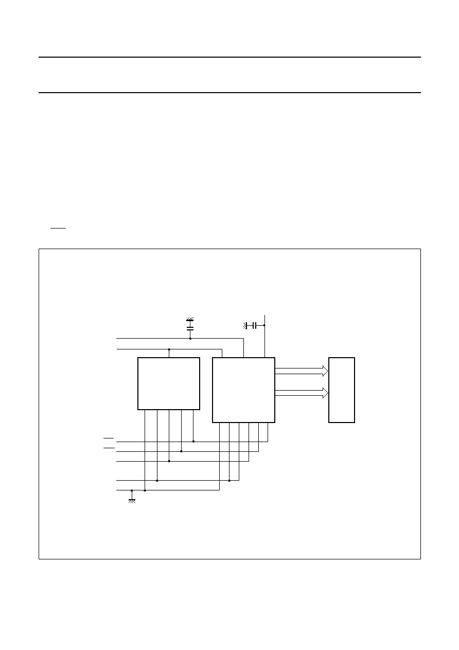
BLOCK DIAGRAM
handbook, full pagewidth
MGU272
DISPLAY DATA RAM
48
◊
84 bits
DATA LATCHES
COLUMN DRIVERS
SHIFT REGISTER
RESET
ROW DRIVERS
COL0 to COL83
OM6211
ROW0 to ROW47
84
3
T4, T5,
T6
TIMING
GENERATOR
SERIAL INTERFACE
CONTROL
DISPLAY
ADDRESS
COUNTER
COMMAND
DECODER
OSCILLATOR
OSC
ADDRESS
COUNTER
SCE
SDIN
SCLK
SDOUT
VLCDOUT
VLCDsense
VLCDIN
VSS2
VSS1
VDD1
VDD2
VDD3
VLCD
GENERATOR
BIAS
VOLTAGE
GENERATOR
RES
48
2
ID3, ID4
MX
3
T1, T2,
T3
5
VOS[4:0]
Fig.1 Block diagram.

2002 Jan 17
5
Philips Semiconductors
Product specification
48
◊
84 dot matrix LCD driver
OM6211
6
PINNING
SYMBOL
PAD
DESCRIPTION
V
OS4
3
input pin 4 for V
LCD
calibration
V
OS3
4
input pin 3 for V
LCD
calibration
V
OS2
5
input pin 2 for V
LCD
calibration
V
OS1
6
input pin 1 for V
LCD
calibration
V
OS0
7
input pin 0 for V
LCD
calibration
T6
8 to 11
test input 6
RES
16
external reset input
(active LOW)
T5
17
test input 5
T4
18
test input 4
T3
19
test output 3
T2
20
test output 2
T1
21
test output 1
SCE
22
chip enable input
(active LOW)
V
SS2
23 to 30
ground
V
SS1
31 to 38
ground
OSC
40
oscillator input
SDOUT
41
serial data output
SDIN
42
serial data input
SCLK
43
serial clock input
ID4
44
module identification input
ID3
45
module identification input
MX
46
horizontal mirroring input
V
DD1
47 to 52
logic supply voltage
V
DD2
53 to 60
voltage multiplier supply
voltage
V
DD3
61 to 64
voltage multiplier supply
voltage
V
LCDSENSE
65
V
LCD
generator regulation
input
V
LCDOUT
66 to 72
V
LCD
generator output
V
LCDIN
73 to 78
LCD supply voltage input
ROW 0 to
ROW 23
89 to 112
LCD row driver outputs
COL 0 to
COL 83
113 to 196
LCD column driver outputs
ROW 47 to
ROW 24
197 to 220
LCD row driver outputs
1, 12 to 15,
39, 79,
81 to 88
and
221 to 225
dummy pads
SYMBOL
PAD
DESCRIPTION
7
PIN FUNCTIONS
7.1
ROW 0 to ROW 47 row driver outputs
These pads output the display row signals.
7.2
COL 0 to COL 83 column driver outputs
These pads output the display column signals.
7.3
V
SS1
and V
SS2
: negative power supply rails
Negative power supply rails V
SS1
and V
SS2
must be
connected together, hereafter referred to as V
SS
. When a
pin has to be connected externally to V
SS
, then pin V
SS1
should be used.
7.4
V
DD1
to V
DD3
: positive power supply rails
Positive power supply rails: V
DD1
for logic supply, V
DD2
and
V
DD3
for voltage multiplier. V
DD2
and V
DD3
must be
connected together, hereafter referred to as V
DD2
.
7.5
V
LCDOUT
, V
LCDIN
and V
LCDSENSE
: LCD power
supply
If the internal V
LCD
generator is used, then all three pins
must be connected together. If not (V
LCD
generator is
disabled and an external voltage is applied to V
LCDIN
), then
V
LCDOUT
must be left open-circuit, V
LCDSENSE
must be
connected to V
LCDIN
, V
DD2
and V
DD3
should be applied
according to the specified voltage range. The following
settings are also required: HVE = 0, S
1
= 1 and S
0
= 0.
7.6
V
OS4
to V
OS0
: calibration inputs
Five pull-up input pins for on-glass V
LCD
calibration. Each
pin may be connected to V
SS
, which corresponds to
logic 0, or left open-circuit, which corresponds to logic 1.
All five pins define a 5-bit two's complement number
ranging from
-
16 to 15 decimal (from 10000 to 01111).
The default value, with all pins connected to V
SS
, is
0 decimal (00000).

2002 Jan 17
6
Philips Semiconductors
Product specification
48
◊
84 dot matrix LCD driver
OM6211
In order to reduce current consumption related to the
pull-up circuitry, the 5-bit number is stored in a register
when exiting the Power-down mode. The pull-up circuitry
is then disabled. Additionally, the register is refreshed by
each HVE command.
7.7
SDIN: serial data input
Serial data input.
7.8
SDOUT: serial data output
Serial data output (3-state, push-pull). If bidirectional data
transmission is required, SDOUT and SDIN should be
connected externally. If the read mode is not used,
SDOUT should be left open-circuit.
7.9
SCLK: serial clock input
Serial clock input.
7.10
SCE: chip enable
Chip enable input, active LOW. If SCE is HIGH, the SCLK
pulses are ignored.
7.11
OSC: oscillator
External clock input. The external clock is active only in a
special test mode, so in the application it is not available.
In normal mode (the internal on-chip oscillator used) this
input must be connected to V
SS
. If OSC is held HIGH, the
internal oscillator is disabled.
7.12
MX: horizontal mirroring
Horizontal mirroring input. When MX = 1 the X address
space is mirrored.
7.13
ID3 and ID4: identification inputs
LCD module identification inputs. Their state can be read
out via the serial interface in order to identify the module
version.
7.14
RES: reset
External reset pin. When LOW the chip will be reset as
defined in Section 9.1. The initialization by the RES pin is
always required during power-on. Timing for the RES pin
is illustrated in Fig.18.
7.15
T1, T2, T3, T4, T5 and T6: test pins
Test pins. In the application T4 and T5 must be connected
to V
SS
. T1, T2, T3 and T6 must be left open-circuit (T6 has
a pull-down resistor).
8
BLOCK DIAGRAM FUNCTIONS
8.1
Oscillator
The on-chip oscillator provides the clock signal for the
display system. It has no external components.
8.2
Serial interface control
Detects the serial interface protocol, commands and
display data bytes. The serial interface converts the data
input (serial-to-parallel) as well as the output bits.
8.3
Command decoder
Decodes all commands.
8.4
Display Data RAM (DDRAM)
The OM6211 contains a 48
◊
84 bit static RAM which
stores the display data. The RAM is divided into six banks
of 84 bytes (6
◊
8
◊
84 bits). During RAM access, data is
transferred to the RAM via the serial interface. There is a
direct correspondence between the X address and column
output number.
8.5
Timing generator
The timing generator produces the various signals
required to drive the internal circuitry. Internal chip
operation is not disturbed by operations of the serial
interface.
8.6
Address Counter (AC)
The address counter assigns addresses to the display
data RAM for writing. The X address (X
6
to X
0
) and the
Y address (Y
2
to Y
0
) are set separately. After a write
operation the address counter is automatically
incremented by 1.
8.7
Display address counter
The display is generated by continuously shifting rows of
RAM data to the dot matrix LCD via the column outputs.
The display status (all dots on/off, normal/inverse video) is
set via the serial interface.
8.8
V
LCD
generator
A voltage multiplier (charge pump) with a programmable
number of stages. Internal capacitors are used for the
voltage multiplier, therefore only decoupling capacitors for
V
LCD
and V
DD2
are required.
2002 Jan 17
7
Philips Semiconductors
Product specification
48
◊
84 dot matrix LCD driver
OM6211
8.9
Bias voltage generator
Generates 4 intermediate LCD bias voltages. The bias
system is selectable; see Section 9.9.
8.10
LCD row and column drivers
The OM6211 contains 48 row and 84 column drivers,
which connect the appropriate LCD bias voltages in
sequence to the display in accordance with the data to be
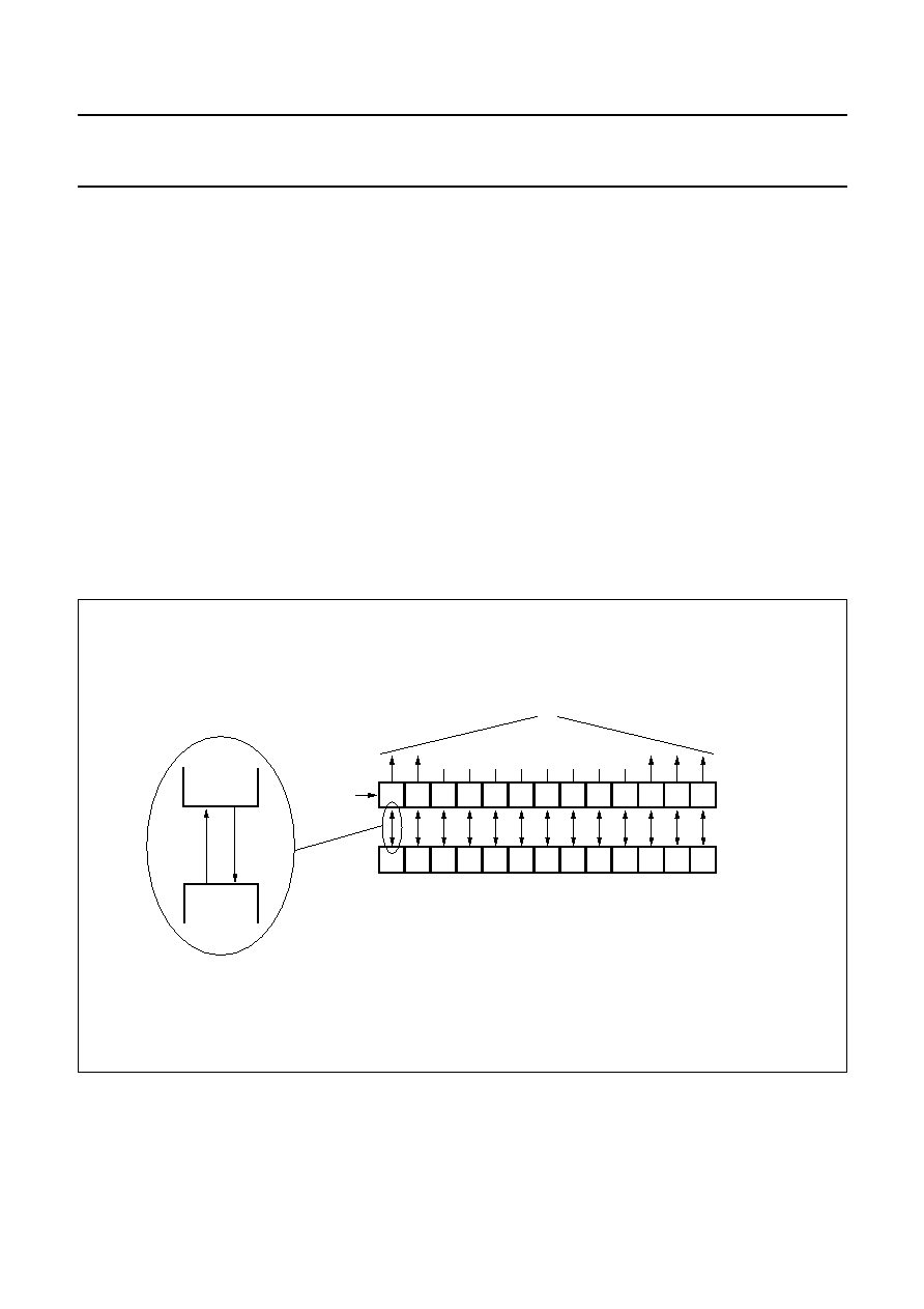
displayed. Figure 3 shows typical waveforms.
8.11
Reset
A reset initializes the chip. It can be performed either by
the RES pin being LOW or by a command.
9
FUNCTIONAL DESCRIPTION
The OM6211 is a low power LCD driver designed to
interface with microprocessors/microcontrollers and a
wide variety of LCDs.
The host microprocessor or microcontroller and the
OM6211 are connected via a serial interface. The internal
oscillator requires no external components. The
appropriate intermediate bias voltages for the multiplexed
LCD waveforms are generated on-chip. The only other
connections required to complete the system are to the
power supplies (V
DD1
, V
DD2
, V
SS
and V
LCD
) and suitable
capacitors for decoupling V
LCD
and V
DD2
.
handbook, full pagewidth
84 column drivers
48 row drivers
LCD
PANEL
MGU273
HOST
MICROPROCESSOR/
MICROCONTROLLER
VSS
VSS1, 2
VLCD
VDD1
VDD2, 3
VDD1
RES
SCE
SCLK
SDA
VSS
VDD2
OM6211
Fig.2 Typical system configuration.

2002 Jan 17
8
Philips Semiconductors
Product specification
48
◊
84 dot matrix LCD driver
OM6211
9.1
Reset
The OM6211 has no internal Power-on reset, only external
reset and reset by command. After power-on an external
reset is required. A reset initiated either from the RES pin
or by command will initialize the chip to the following
starting conditions:
∑
Power-down mode (DON = 0 and DAL = 1):
≠ Internal oscillator stopped
≠ The V
LCD
generator (HV generator) is switched off
(HVE = 0) and V
LCDOUT
is 3-state
≠ Display is off and all LCD outputs are internally
connected to V
SS
(DON = 0)
≠ Display all points is on (DAL = 1).
∑
Serial interface initialized; write mode
∑
Display normal video (E = 0)
∑
Address counter X
6
to X
0
= 0; Y
2
to Y
0
= 0; display start
line Z
5
to Z
0
= 0; no Y mirroring (MY = 0)
∑
Bias system
1
/
7
(BS
2
to BS
0
= 100)
∑
V
LCD
selection V
PR7
to V
PR0
= 0
∑
Voltage multiplication factor 4 (S
1
and S
0
= 10)
∑
Temperature control mode TC3 (TC
1
and TC
0
= 11)
∑
Frequency not calibrated and OC = 0
∑
RAM data is unchanged (after power-up undefined).
9.2
Power-down
The chip is in Power-down mode if the display is off
(DON = 0) and display all points is on (DAL = 1),
regardless of the order in which both bits are set. During
the Power-down mode almost all static currents are
switched off (no internal oscillator, no timing and no LCD
segment drive system), and all LCD outputs are internally
connected to V
SS
. The V
LCD
generator is switched off (but
HVE is not affected). The serial interface function remains.
RAM data is unchanged. When exiting the Power-down
mode, the V
OS
value is stored in a register.
9.3
LCD voltage selector
The practical value for V
LCD
is determined by equating
V
off(rms)
with a defined LCD threshold voltage (V
th
),
typically when the LCD exhibits approximately 10%
contrast.
9.4
Oscillator
The internal logic operation and the multi-level drive
signals of the OM6211 are clocked by the built-in RC
oscillator. No external components are required. The
oscillator is in operation as long as the chip is not in
Power-down mode.
9.5
Timing
The timing of the OM6211 organizes the internal data flow
of the device. The timing also generates the LCD frame
frequency that is derived from the clock frequency
generated by the internal clock generator.
9.6
Column driver outputs
The LCD drive section includes 84 column outputs, which
should be connected directly to the LCD. The column
output signals are generated in accordance with the
multiplexed row signals and with the data in the display
latch. If less than 84 columns are required, the unused
column outputs should be left open-circuit.
9.7
Row driver outputs
The LCD drive section includes 48 row outputs, which
should be connected directly to the LCD. If less than
48 rows are required, the unused row outputs should be
left open-circuit.

2002 Jan 17
9
Philips Semiconductors
Product specification
48
◊
84 dot matrix LCD driver
OM6211
9.8
Drive waveforms
MGU274
ROW 0
R0 (t)
ROW 1
R1 (t)
COL 0
C0 (t)
COL 1
C1 (t)
0 V
0 V
V3
-
VSS
frame n
frame n
+
1
0 1 2 3 4 5 6 7 8...
... 47 0 1 2 3 4 5 6 7 8...
... 47
Vstate1(t)
Vstate1(t)
Vstate2(t)
VLCD
V2
V3
V4
V5
VSS
VLCD
V2
V3
V4
V5
VSS
VLCD
V2
V3
V4
V5
VSS
VLCD
V2
V3
V4
V5
VSS
VLCD
VLCD
-
V2
V4
-
V5
VSS
-
V5
V4
-
VLCD
V3
-
V2
-
VLCD
0 V
0 V
V3
-
VSS
Vstate2(t)
VLCD
VLCD
-
V2
V4
-
V5
V4
-
VLCD
V3
-
V2
VSS
-
V5
-
VLCD
Fig.3 Typical LCD driver waveforms.
V
state1
(t) = C1(t)
-
R0(t).
V
state2
(t) = C1(t)
-
R1(t).
2002 Jan 17
10
Philips Semiconductors
Product specification
48
◊
84 dot matrix LCD driver
OM6211
9.9
Bias system
The bias voltage levels are set in the ratio of
R - R - nR - R - R. Different multiplex rates require
different factors of n. This is programmed by BS
2
to BS
0
.
For optimum bias values, n can be calculated from the
following equation:
; where Mux rate is 48.
Changing the bias system from the optimum setting will
have a consequence on the contrast and viewing angle.
One reason to depart from the optimum would be to
reduce the required V
LCD
voltage. A compromise between
contrast and V
LCD
must be found for any particular
application.
In the OM6211 one of three possible values of the bias
system can be selected. The value
1
/
7
is default.
n
Mux rate
3
≠
=
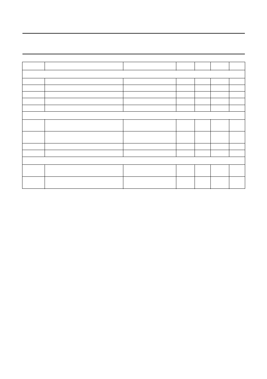
Table 1
Programming the required bias system
Table 2
LCD bias voltages for
1
/
6
bias,
1
/
7
bias and
1
/
8
bias.
9.10
Voltage multiplier control
The OM6211 incorporates a software configurable voltage multiplier. After reset (RES) the voltage multiplier is set to
4V
DD2
. Other voltage multiplier factors are set via the serial interface (S
1
and S
0
).
Table 3
HV generator multiplication
BS
2
BS
1
BS
0
n
BIAS MODE
TYPICAL MUX
RATES
0
1
1
4
1
/
8
1 : 55 and 1 : 48
1
0
0
3
1
/
7
1 : 33
1
0
1
2
1
/
6
1 : 24
SYMBOL
BIAS VOLTAGE
FOR
1
/
6
BIAS
FOR
1
/
7
BIAS
FOR
1
/
8
BIAS
V1
V
LCD
V
LCD
V
LCD
V2
5
/
6
V
LCD
6
/
7
V
LCD
7
/
8
V
LCD
V3
4
/
6
V
LCD
5
/
7
V
LCD
6
/
8
V
LCD
V4
2
/
6
V
LCD
2
/
7
V
LCD
2
/
8
V
LCD
V5
1
/
6
V
LCD
1
/
7
V
LCD
1
/
8
V
LCD
V6
V
SS
V
SS
V
SS
S
1
S
0
MULTIPLICATION
0
0
2V
DD2
0
1
3V
DD2
1
0
4V
DD2
1
1
not available
2002 Jan 17
11
Philips Semiconductors
Product specification
48
◊
84 dot matrix LCD driver
OM6211
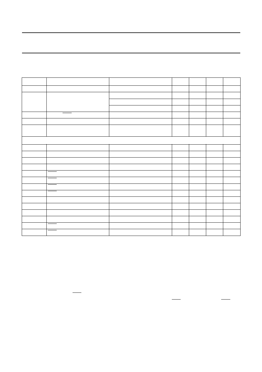
9.11
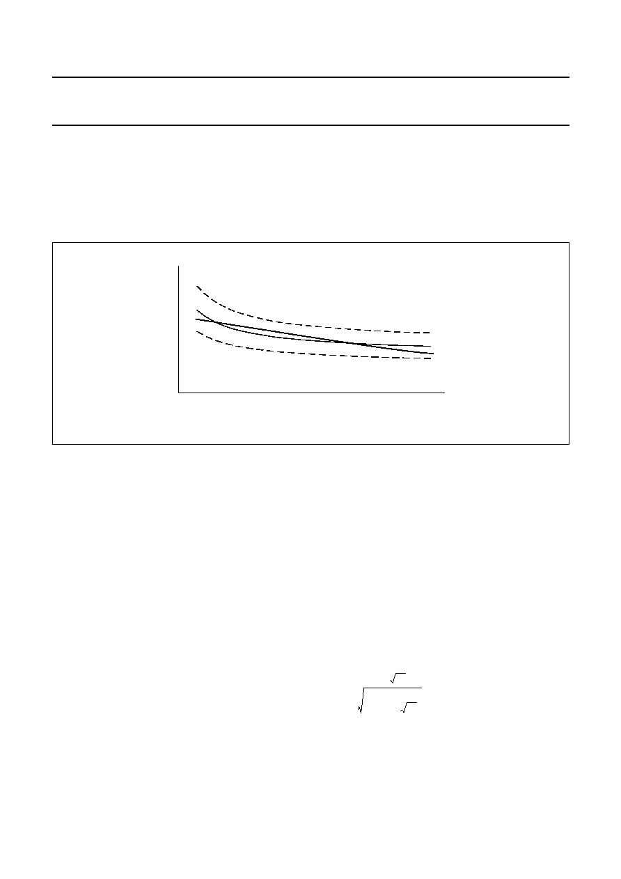
Temperature compensation
Due to the temperature dependency of the liquid crystals viscosity, the LCD controlling voltage (V
LCD
) must be increased
at lower temperatures to maintain optimum contrast. Figure 4 shows V
LCD
as a function of temperature for a typical high
multiplex rate liquid.
In the OM6211 the temperature coefficient of V
LCD
can be selected from 4 values by setting bits TC
1
and TC
0
,
see Tables 4 and 8.
handbook, full pagewidth
MGT848
T
VLCD
Fig.4 V
LCD
as a function of liquid crystal temperature (typical values).
9.12
V
LCD
generator
The binary number V
OP
representing the operating voltage
can be set by the serial interface command and can be
adjusted (calibrated) by 5 input pins according to the
following formula:
(1)
where:
∑
V
PR
is an 8-bit unsigned number set by the serial
interface command
∑
V
OS
is a 5-bit two's complement number set by the
5 input pins V
OS4
to V
OS0
, see Table 9
∑
V
OP
is an 8-bit unsigned number used internally for
generation of the LCD supply voltage V
LCD
.
To avoid numerical overflow the allowed values of V
PR
should be limited to the range 32 to 225 (decimal).
The corresponding voltage at the reference temperature,
T
nom
, can be calculated as follows:
(2)
The generated voltage at V
LCD
is dependent on the
temperature, programmed Temperature Coefficient (TC)
and the programmed voltage at the reference temperature
(T
nom
).
(3)
T
nom
, a and b for each temperature coefficient are given in
Table 4. The maximum voltage that can be generated is
dependent on the voltage of V
DD2
and the display load
current.
As the programming range for the internally generated
V
LCD
allows values above the maximum allowed V
LCD
, the
user has to ensure while setting the V
PR
register and
selecting the Temperature Compensation, that under all
conditions and including all tolerances the V
LCD
limit of
maximum 9 V will never be exceeded.
For a particular liquid crystal, the optimum value of V
LCD
can be calculated for a given multiplex rate. For a Mux rate
of 1 : 48, the optimum operating voltage of the liquid
crystal can be calculated as follows;
(4)
where V
th
is the threshold voltage of the liquid crystal used.
V
OP
V
PR
V
OS
+
=
V
LCD(Tnom)
a
V
OP
b
◊
+
(
)
=
V
LCD
a
V
OP
+
b
◊
(
)
1
TC
T
T
nom
≠
(
)
◊
+
[
]
◊
=
V
LCD
1
48
+
2
1
1
48
----------
≠
◊
---------------------------------------
V
th
◊
6.06
V
th
◊
=
=

2002 Jan 17
12
Philips Semiconductors
Product specification
48
◊
84 dot matrix LCD driver
OM6211
Table 4
Typical values for parameters of the HV generator programming
Example: to achieve V
LCD
= 8.3 V at temperature T
nom
for TC3 it is necessary to set V
PR
= 180 (decimal).
Example for calibration: Before calibration V
PR
= 180 was applied, but the measured voltage was V
LCD
= 8.4 V.
To decrease V
LCD
by 100 mV the best value for V
OS
is
-
4 decimal (11100 binary in the two's complement notation). So
after calibration with V
OS
=
-
4 the proper V
PR
value is still 180.
As V
OS
is used for calibration and the default value is 0, for selecting the value of V
PR
it can always be considered that
V
OS
= 0.
SYMBOL
TC0
TC1
TC2
TC3
UNIT
a
4.57
4.28
4.04
3.79
V
b
30.0
28.0
26.5
25.0
mV
T
nom
27
27
27
27
∞
C
TC
0
-
0.25
-
0.5
-
0.75
10
-3
/
∞
C
handbook, full pagewidth
MGT847
00
01
02
a
VLCD
VOP
03
04
05
06
. . .
. . .
FD
FE
FF
b
Fig.5 V
LCD
programming of OM6211.
V
OP7
to V
OP0
programming, (00H to FFH).

2002 Jan 17
13
Philips Semiconductors
Product specification
48
◊
84 dot matrix LCD driver
OM6211
10 INITIALIZATION
10.1
Initialization sequence
After reset (RES) it is recommended to initialize the V
LCD
generator using the following sequence; a starting state of
HVE = 0, DON = 0 and DAL = 1 is assumed:
1. Set the required V
OP
and, if required, the voltage
multiplier S
1
and S
0
2. Set DAL = 0 to leave the Power-down state (in order to
precharge the charge pump V
LCD
is set to V
DD2
)
3. Wait for at least 1 ms and set HVE = 1 to switch-on the
V
LCD
generator
4. Set DON = 1 to switch the display on.
10.2
Frame frequency calibration (OC)
The OM6211 incorporates frame frequency calibration via
software. The calibration is achieved by tuning the internal
oscillator. After reset the frame frequency calibration is
disabled (OC = 0). The calibration can only be performed
if the driver is not in Power-down mode. The calibration is
started by setting OC = 1 via the serial interface (start
command) and will be stopped by setting OC = 0 (stop
command). The time between start and stop of the
calibration must be 200 ms to give a frame frequency of
80 Hz. Any variation in calibration time (deviation from
200 ms) results in a corresponding variation in frame
frequency. During calibration all other commands are
allowed.
The calibration may be repeated and is always performed
with the previously calibrated frequency. Through
repeated calibrations a better accuracy can be expected
and, most especially, the temperature drift can be
compensated for. A minimum time delay of 500 ms
between consecutive calibration events is necessary
(between stop and start).
The calibration will always be performed if the calibration
time is between 190 and 210 ms. If, however, the
calibration time is lower then 58 ms or higher than 690 ms
(or the stop command does not occur at all), the calibration
attempt is ignored and the previously selected frequency is
maintained. For the remaining values of the calibration
time (from 58 to 190 ms and from 210 to 690 ms) it cannot
be determined if the calibration will be performed or
ignored.
11 ADDRESSING
11.1
Addressing
Data is downloaded in bytes into the RAM matrix of
OM6211 as illustrated in Figs 6 and 7. The display RAM
has a matrix of 48
◊
84 bits. The columns are addressed
by the address pointer. The address ranges are
X = 0 to 83 (1010011) and Y = 0 to 5 (101). Addresses
outside of these ranges are not allowed. The X address
increments after each byte (see Fig.7). After the last
X address (X = 83) X wraps around to 0 and Y increments
to address the next row. After the very last address (X = 83
and Y = 5) the address pointers wrap around to address
X = 0 and Y = 0.
The selection of the MX input allows horizontal mirroring:
when MX = 1, the X address space is mirrored (see Fig.6).
When MX = 0 the mirroring is disabled. MX affects data
only during writing to the RAM, so after a change of MX
RAM data must be re-written.
The MY bit allows vertical mirroring: when MY = 1, then
the Y address space is mirrored. MY does not affect the
RAM content, but defines the way RAM data is written to
the display. A change of MY has an immediate effect on
the display.
Vertical scrolling of the display is controlled by the
Z address with a range from 0 to 47 (101111). The
Z address specifies which rows of the RAM are output to
which row outputs. The value of the Z address defines
which row of the RAM will be ROW 0 of the display (which
is normally the top row of the display). For example, if the
Z address is set to 31 (see Fig.8), then the data displayed
on ROW 0 of the display will be the data from ROW 31 of
the RAM and the data on ROW 1 will be from ROW 32 of
the RAM. When the MY is active (MY = 1), then the
Z address defines which row of the RAM is written to
ROW 47 of the display. For example, when the Z address
is set to 31, ROW 47 of the display would come from
ROW 31 of the RAM and ROW 46 from ROW 32 of the
RAM (see Fig.9).
The Z address does not affect the RAM content, but
defines the way RAM data is written to the display.
A change of Z address has an immediate effect on the
display.

2002 Jan 17
14
Philips Semiconductors
Product specification
48
◊
84 dot matrix LCD driver
OM6211
handbook, full pagewidth
MGU275
0
5
0
83
83
0
X address
Y address
LSB
MSB
MX = 0
MX = 1
Fig.6 RAM format, addressing.
handbook, full pagewidth
MGT845
0
1
2
84
85
86
168
169
170
252
253
254
336
337
338
420
421
422
0
5
503
0
83
X address
Y address
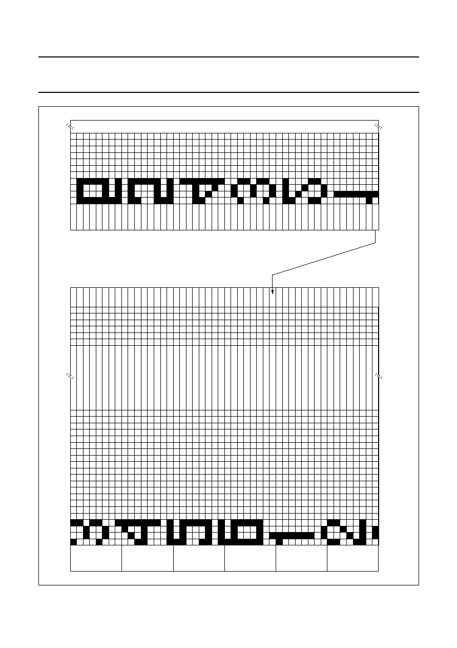
Fig.7 Sequence of writing data bytes into RAM.

2002
Jan
17
15
Philips Semiconductors
Product specification
48
◊
84 dot matr
ix LCD dr
iv
er
OM6211
This text is here in white to force landscape pages to be rotated correctly when browsing through the pdf in the Acrobat reader.This text is here in
_
white to force landscape pages to be rotated correctly when browsing through the pdf in the Acrobat reader.This text is here inThis text is here in
white to force landscape pages to be rotated correctly when browsing through the pdf in the Acrobat reader. white to force landscape pages to be ...
ROW 0
ROW 1
ROW 2
ROW 3
ROW 4
ROW 5
ROW 6
ROW 7
ROW 8
ROW 9
ROW 10
ROW 11
ROW 12
ROW 13
ROW 14
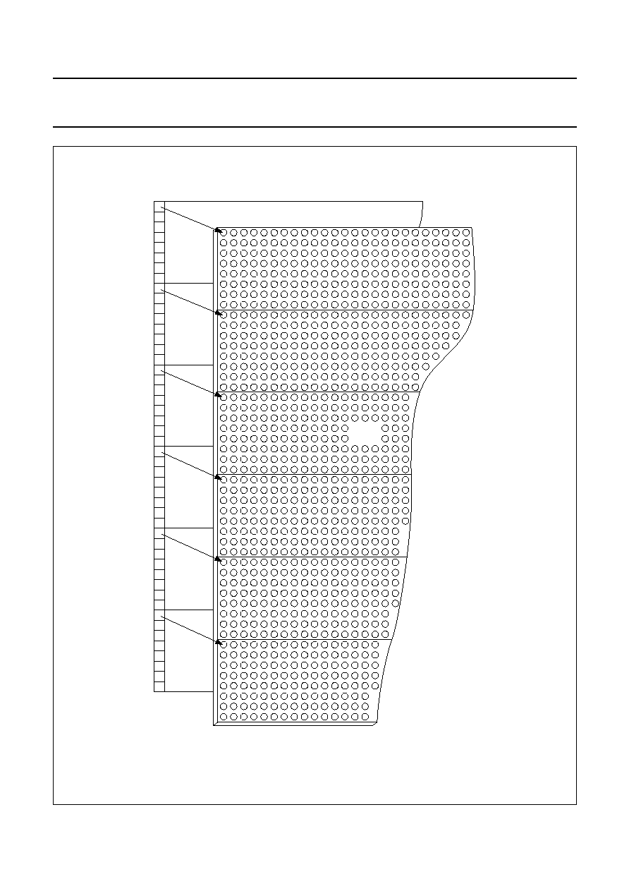
ROW 15
ROW 16
ROW 17
ROW 18
ROW 19
ROW 20
ROW 21
ROW 22
ROW 23
ROW 24
ROW 25
ROW 26
ROW 27
ROW 28
ROW 29
ROW 30
ROW 31
ROW 32
ROW 33
ROW 34
ROW 35
ROW 36
ROW 37
ROW 38
ROW 39
ROW 40
ROW 41
ROW 42
ROW 43
ROW 44
ROW 45
ROW 46
ROW 47
0
1
2
3
4
5
6
7
8
9
10
11
12
13
14
15
16
17
18
19
20
21
22
23
24
25
26
27
28
29
30
31
32
Z address = 31
0
Y address
Z address when MY = 0
RAM
DISPLAY
MGU276
1
2
3
4
5
33
34
35
36
37
38
39
40
41
42
43
44
45
46
47
Fig.8 Programming the Z address when MY = 0.
2002
Jan
17
16
Philips Semiconductors
Product specification
48
◊
84 dot matr
ix LCD dr
iv
er
OM6211
This text is here in white to force landscape pages to be rotated correctly when browsing through the pdf in the Acrobat reader.This text is here in
_
white to force landscape pages to be rotated correctly when browsing through the pdf in the Acrobat reader.This text is here inThis text is here in
white to force landscape pages to be rotated correctly when browsing through the pdf in the Acrobat reader. white to force landscape pages to be ...
0
1
2
3
4
5
6
7
8
9
10
11
12
13
14
15
16
17
18
19
20
21
22
23
24
25
26
27
28
29
30
31
32
Z address = 31
0
Y address
Z address with MY = 1
RAM
DISPLAY
MGU277
1
2
3
4
5
33
34
35
36
37
38
39
40
41
42
43
44
45
46
47
ROW 0
ROW 1
ROW 2
ROW 3
ROW 4
ROW 5
ROW 6
ROW 7
ROW 8
ROW 9
ROW 10
ROW 11
ROW 12
ROW 13
ROW 14
ROW 15
ROW 16
ROW 17
ROW 18
ROW 19
ROW 20
ROW 21
ROW 22
ROW 23
ROW 24
ROW 25
ROW 26
ROW 27
ROW 28
ROW 29
ROW 30
ROW 31
ROW 32
ROW 33
ROW 34
ROW 35
ROW 36
ROW 37
ROW 38
ROW 39
ROW 40
ROW 41
ROW 42
ROW 43
ROW 44
ROW 45
ROW 46
ROW 47
Fig.9 Programming the Z address when MY = 1.
2002 Jan 17
17
Philips Semiconductors
Product specification
48
◊
84 dot matrix LCD driver
OM6211
top of LCD
MGT842
DDRAM
bank 0
bank 1
bank 2
R0
R8
R16
R24
R32
R40
R47
bank 3
bank 4
bank 5
LCD
Fig.10 DDRAM to display mapping (Z = 0).

2002 Jan 17
18
Philips Semiconductors
Product specification
48
◊
84 dot matrix LCD driver
OM6211
11.2
Serial interface
The serial interface is a 3-line bidirectional interface for
communication between the microcontroller and the LCD
driver chip. The 3 lines are: SCE (chip enable), SCLK
(serial clock) and SDA (serial data). The OM6211 is
connected to SDA by two pins: SDIN (data input) and
SDOUT (data output) connected together.
11.2.1
W
RITE MODE
The write mode of the interface means that the
microcontroller writes commands and data to the OM6211.
Each data packet contains a control bit D/C and a
transmission byte. If D/C is LOW, the following byte is
interpreted as a command byte (see Table 5). If D/C is
HIGH, the following byte is stored in the display data RAM.
After every data byte the address counter is incremented
automatically. Figure 11 shows the general format of the
write mode and the definition of the transmission byte.
Every command can be sent in any order to the OM6211.
The MSB of a byte is transmitted first. The serial interface
is initialized when SCE is HIGH. In this state, SCLK clock
pulses have no effect and no power is consumed by the
serial interface. A falling edge on SCE enables the serial
interface and indicates the start of a data transmission.
Figures 12, 13 and 14 show the protocol of the write
mode:
∑
When SCE is HIGH, SCLK clocks are ignored: during
the HIGH time of SCE the serial interface is initialized
(see Fig.12)
∑
At the falling edge of SCE SCLK must be LOW (see
Fig.16); for the transmission of each data bit a rising and
then a falling edge of SCLK is necessary
∑
SDIN is sampled at the rising edge of SCLK
∑
D/C indicates whether the byte is a command (D/C = 0)
or RAM data (D/C = 1); it is sampled with the first rising
SCLK edge
∑
If SCE stays LOW after the last bit of a command or data
byte, the serial interface expects the D/C bit of the next
byte at the next rising edge of SCLK (see Fig.13)
∑
A reset pulse with RES interrupts the transmission. The
data being written into the RAM may be corrupted. The
registers are cleared. If SCE is LOW after the rising
edge of RES, the serial interface is ready to receive the
D/C bit of a command or data byte (see Fig.14).
handbook, full pagewidth
D/C DB7 DB6 DB5 DB4 DB3
Transmission Byte (TB) (command byte OR data byte)
DB2 DB1 DB0
MSB
LSB
MGU278
TB
D/C
TB
D/C
TB
D/C
Fig.11 Serial data stream, write mode.

2002 Jan 17
19
Philips Semiconductors
Product specification
48
◊
84 dot matrix LCD driver
OM6211
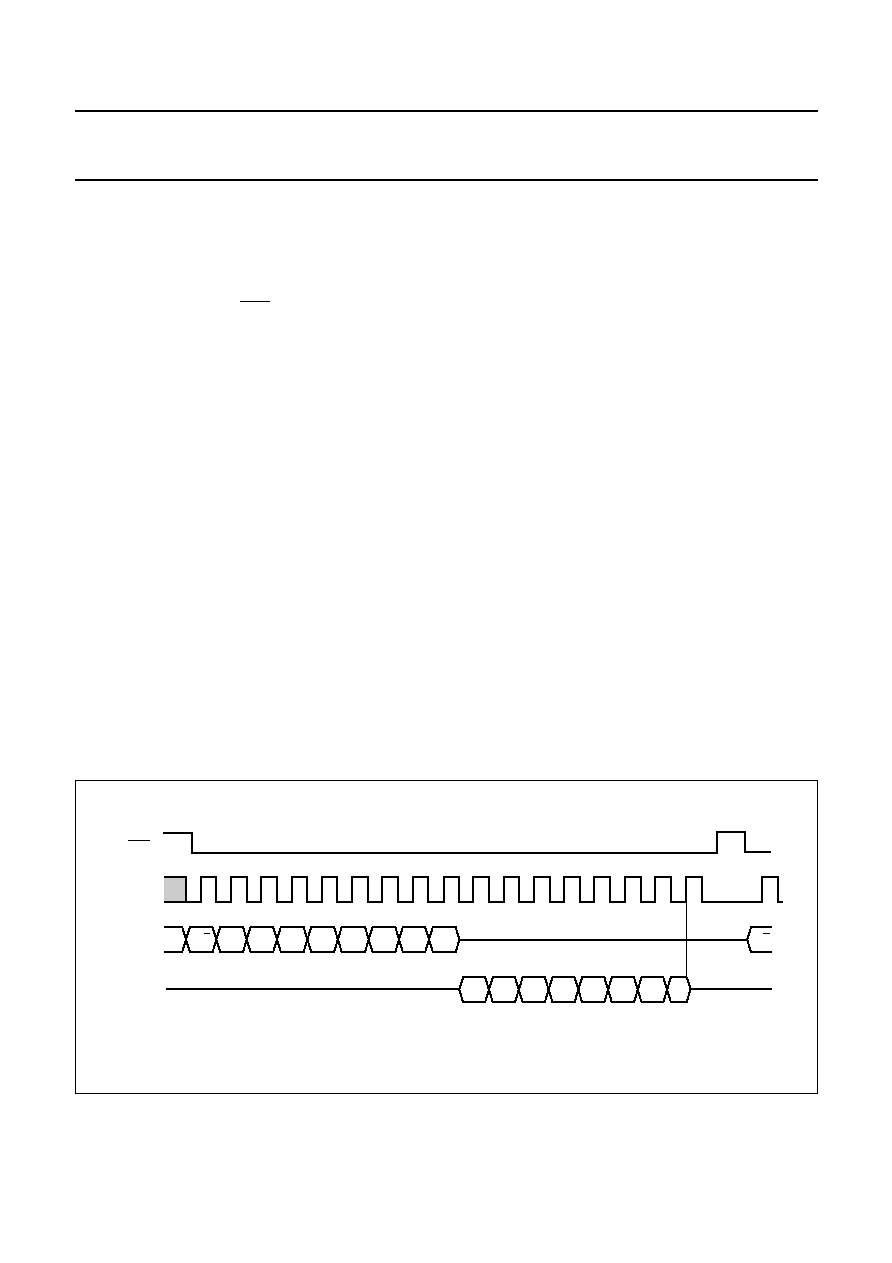
handbook, full pagewidth
SCE
D/C
SCLK
SDIN
DB7
DB6
DB5
DB4
DB3
DB2
DB1
DB0
MGU279
Fig.12 Write mode: a control bit followed by a transmission byte.
handbook, full pagewidth
SCE
SCLK
SDIN
DB7
D/C
DB6 DB5 DB4 DB3 DB2
DB1 DB0
MGU280
DB7
D/C
DB6 DB5 DB4 DB3 DB2
DB1 DB0 D/C
Fig.13 Write mode: transmission of several bytes.
handbook, full pagewidth
MGU281
SCE
RES
SCLK
SDIN
DB7
D/C
DB6 DB5 DB4
DB7
DB7 DB6 DB5 DB4 DB3 DB2
DB1 DB0
DB6
D/C
D/C
Fig.14 Write mode: interrupted by reset (RES).
2002 Jan 17
20
Philips Semiconductors
Product specification
48
◊
84 dot matrix LCD driver
OM6211
11.2.2
R
EAD MODE
In the read mode of the interface the microcontroller reads
data from the OM6211. To do so the microcontroller first
has to send the read status command, and then the
following byte is transmitted in the opposite direction
(using SDOUT). After that SCE is required to go HIGH
before a new command is sent (see Fig.15).
The OM6211 samples the SDIN data on the rising edges
of SCLK, but shifts SDOUT data on the falling edges of
SCLK. Thus the microcontroller is supposed to read
SDOUT data on the rising edges of SCLK.
After the read status command has been sent, the SDIN
line must be set to 3-state not later then the falling SCLK
edge of the last bit (see Fig.15).
The 8th read bit is shorter than the others because it is
terminated by the rising edge of SCLK (see Fig.15). The
last rising edge of SCLK sets SDOUT to 3-state after the
delay time t
3
(see Section 10.1 and Fig.17).
There are 5 bits of information only that can be read by the
microcontroller (see Table 7). Two of them are chip
identification bits and have fixed values. The next two bits
are LCD module identification bits and can be set by
connecting the ID3 and ID4 pins to V
DD1
or V
SS
. The fifth
bit is the V
LCD
voltage monitor bit VM.
It indicates that the charge pump is running and the
voltage level of V
LCD
is sufficient to provide enough
contrast of the display (VM = 1). If the V
LCD
generator
cannot produce a voltage defined by V
OP
, then VM = 0.
VM has a valid value 45 ms after a delay time of
approximately 45 ms starting from the time the V
LCD
generator has been switched on (by setting HVE = 1). This
delay time is dependent on the external V
LCD
decoupling
capacitor (here 100 nF is assumed).
For more details concerning the VM bit see Chapter 22
The reading out of the chip identification bits and module
identification bits can be used to implement different
initialization schemes for different applications. The
reading out of VM can be used to check the proper
electrical contacts of the LCD module.
One read status command enables one status bit to be
read, i.e. 5 commands are needed to read the status of all
5 bits. The first 4 bits of the read byte (DB7 to DB4) are
always equal to the corresponding status bit and the next
4 bits (DB3 to DB0) are equal to the complement of this bit.
As stated before the SDOUT data is supposed to be read
on the rising edge of SCLK. Care must be taken, however,
when running the SCLK at maximum frequency. Because
of the access time limit t
2
(see Section 10.1 and Fig.17) it
might happen that the first bits of each group (DB7 to DB4
and DB3 to DB0) are not valid at the time of the
corresponding SCLK edges. Thus it is recommended to
read the bits DB4 and DB0 only.
handbook, full pagewidth
MGU282
SCE
SCLK
SDIN
SDOUT
DB7
D/C
DB6 DB5 DB4
DB7 DB6 DB5 DB4 DB3 DB2 DB1
DB0
DB3 DB2
DB1 DB0
D/C
Fig.15 Read mode.

2002 Jan 17
21
Philips Semiconductors
Product specification
48
◊
84 dot matrix LCD driver
OM6211
12 INSTRUCTIONS
12.1
Instruction set
Table 5
Instruction set; see notes 1 and 2 and Table 6
Notes
1. X = don't care.
2. DB7 = MSB.
INSTRUCTION
D/C
COMMAND BYTE
DESCRIPTION
DB7
DB6
DB5
DB4
DB3
DB2
DB1
DB0
NOP
0
1
1
1
0
0
0
1
1
no operation
Reset
0
1
1
1
0
0
0
1
0
software reset
Write data
1
D
7
D
6
D
5
D
4
D
3
D
2
D
1
D
0
write data to display RAM
Read status
0
1
1
0
1
1
SB2
SB1
SB0
read one of the status bits; Table 7
Display control
0
1
0
1
0
1
1
1
DON display on/off; see Table 6
0
1
0
1
0
0
1
1
E
normal, reverse mode; see Table 6
0
1
0
1
0
0
1
0
DAL
all pixels on; see Table 6
0
1
1
0
0
MY
X
X
X
mirror Y; see Table 6
Address
commands
0
1
0
1
1
0
Y
2
Y
1
Y
0
set Y address; 0
Y
5
0
0
0
0
1
X
X
6
X
5
X
4
set X address; 0
X
83
0
0
0
0
0
X
3
X
2
X
1
X
0
set X address; 0
X
83
Display start line
0
0
1
Z
5
Z
4
Z
3
Z
2
Z
1
Z
0
set start ROW, 0
Z
47
Power control
0
0
0
1
0
1
HVE
HVE
HVE
switch HV-gen on/off; see Table 6
0
1
0
0
V
PR4
V
PR3
V
PR2
V
PR1
V
PR0
lower part of V
PR
; see Equation (1)
0
0
0
1
0
0
V
PR7
V
PR6
V
PR5
higher part of V
PR
Frame
calibration
0
1
0
1
0
1
1
0
OC
frame calibration start/stop;
see Table 6
TC
0
0
0
1
1
1
0
TC1
TC0
set temperature coefficient;
see Table 8
HV-gen stages
0
0
0
1
1
1
1
S
1
S
0
set multiplication factor;
see Table 3
Bias system
0
0
0
1
1
0
BS2
BS1
BS0
set bias system; see Table 1
Test
0
1
0
1
0
1
0
0
X
reserved
0
1
1
1
0
1
0
1
1
reserved
0
1
1
1
0
1
1
0
0
reserved
0
1
1
1
0
1
1
1
1
reserved
2002 Jan 17
22
Philips Semiconductors
Product specification
48
◊
84 dot matrix LCD driver
OM6211
Table 6
Explanations for symbols in Table 5
BIT
LOGIC 0
LOGIC 1
DON
display off
display on
DAL
normal display (only if DON = 1)
all pixels on
E
normal display
inverse video mode (only if DAL = 0)
HVE
V
LCD
generator (HV generator) is switched off
V
LCD
generator is switched on
MY
no Y mirroring
Y mirroring
OC
stop frame frequency calibration
start frame frequency calibration
Table 7
Read status
Table 8
Temperature coefficients
Table 9
V
OS
values in two's complement notation
SB[2:0]
READ
STATUS BIT
DESCRIPTION
010
ID1
fixed value 0
011
ID2
fixed value 1
100
ID3
defined by input pin ID3
101
ID4
defined by input pin ID4
111
VM
VM
TC[1:0]
00
TC0
01
TC1
10
TC2
11
TC3
DECIMAL
BINARY
+0
00000
+1
00001
+2
00010
+3
00011
+4
00100
+5
00101
+6
00110
+7
00111
+8
01000
+9
01001
+10
01010
+11
01011
+12
01100
+13
01101
+14
01110
+15
01111
-
1
11111
-
2
11110
-
3
11101
-
4
11100
-
5
11011
-
6
11010
-
7
11001
-
8
11000
-
9
10111
-
10
10110
-
11
10101
-
12
10100
-
13
10011
-
14
10010
-
15
10001
-
16
10000
DECIMAL
BINARY
2002 Jan 17
23
Philips Semiconductors
Product specification
48
◊
84 dot matrix LCD driver
OM6211
13 LIMITING VALUES
In accordance with the Absolute Maximum Rating System (IEC 60134); notes 1 and 2.
Notes
1. Stresses above those listed under limiting values may cause permanent damage to the device.
2. Parameters are valid over operating temperature range unless otherwise specified. All voltages are referenced to
V
SS
unless otherwise specified.
3. V
SS
= 0 V.
14 HANDLING
Inputs and outputs are protected against electrostatic discharge in normal handling. However, to be totally safe, it is
recommended to take normal precautions appropriate to handling MOS devices (see
"Handling MOS Devices").
15 DC CHARACTERISTICS
V
DD1
= 1.7 to 2.3 V; V
DD2
= 2.5 to 4.5 V; V
SS
= 0 V; V
LCD
= 4.5 to 9.0 V; T
amb
=
-
40 to +85
∞
C; unless otherwise
specified.
SYMBOL
PARAMETER
CONDITIONS
MIN.
MAX.
UNIT
V
DD
supply voltage
-
0.5
+6.5
V
V
LCD
LCD supply voltage
-
0.5
+9.0
V
V
I
, V
O
input/output voltage (any input/output)
-
0.5
V
DD1
+ 0.5
V
I
I
, I
O
DC input or output current
-
10
+10
mA
I
DD
, I
SS
, I
LCD
V
DD
, V
SS
or V
LCD
current
note 3
-
50
+50
mA
P
tot
total power dissipation per package
-
100
mW
P
out
power dissipation per output
-
10
mW
T
stg
storage temperature
-
65
+150
∞
C
T
j(max)
maximum junction temperature
-
150
∞
C
SYMBOL
PARAMETER
CONDITIONS
MIN.
TYP.
MAX.
UNIT
Supplies
V
DD1
logic supply voltage
1.7
1.8
2.3
V
V
DD2,
V
DD3
supply voltage for voltage multiplier
note 1
2.5
2.78
4.5
V
V
LCDIN
LCD supply voltage
4.5
-
9.0
V
V
LCDOUT
generated LCD supply voltage
note 2
6.8
-
-
V
V
LCD(tol)
tolerance of generated V
LCD
with calibration; note 3
-
70
-
+70
mV
I
DD1
V
DD1
supply current
Power-down mode; note 4
-
2
10
µ
A
normal mode; note 4
-
12
-
µ
A
I
DD2,
I
DD3
V
DD2
and V
DD3
supply current
Power-down mode; note 4
-
1
5
µ
A
normal mode; note 4
-
78
-
µ
A
I
DD(tot)
total supply current (V
DD1
and V
DD2,
V
DD3
)
normal mode; note 4
-
90
-
µ
A
normal mode; note 5
-
120
-
µ
A
2002 Jan 17
24
Philips Semiconductors
Product specification
48
◊
84 dot matrix LCD driver
OM6211
Notes
1. V
DD2
is always equal V
DD3
.
2. Conditions are: V
DD2
= 2.5 V, voltage multiplier = 3V
DD2
, bias system
1
/
6
, V
LCD
output is loaded by 10
µ
A,
T
amb
= 25
∞
C.
3. Valid for values of temperature, V
PR
and TC used at the calibration.
4. Conditions are: V
DD1
= 1.8 V, V
DD2
= 2.78 V, V
LCD
= 6.8 V, voltage multiplier = 3V
DD2
, bias system
1
/
6
, inputs at V
DD1
or V
SS
, serial interface inactive, internal V
LCD
generation, V
LCD
output is loaded by 10
µ
A; T
amb
= 25
∞
C.
5. Conditions are: V
DD1
= 1.8 V, V
DD2
= 2.78 V, V
LCD
= 8.3 V, voltage multiplier = 4V
DD2
, bias system
1
/
7
, inputs at V
DD1
or V
SS
, serial interface inactive, internal V
LCD
generation, V
LCD
output is loaded by 10
µ
A; T
amb
= 25
∞
C.
6. Load current 10
µ
A, outputs tested one at a time.
Logic
V
IL
LOW-level input voltage
V
SS
-
0.3V
DD1
V
V
IH
HIGH-level input voltage
0.7V
DD1
-
V
DD1
V
I
OL
LOW-level output current (SDOUT)
V
OL
= 0.4 V; V
DD1
= 1.8 V
0.5
-
-
mA
I
OH
HIGH-level output current (SDOUT)
V
OH
= 1.4 V; V
DD1
= 1.8 V
-
-
-
0.5
mA
I
L
leakage current
V
I
= V
DD1
or V
SS
-
1
-
+1
µ
A
Column and row outputs
R
o(col)
column output resistance (COL 0 to
COL 83)
note 6
-
4
20
k
R
o(row)
row output resistance (ROW 0 to
ROW 47)
note 6
-
4
20
k
V
bias(col)
bias tolerance (COL 0 to COL 83)
-
100
0
+100
mV
V
bias(row)
bias tolerance (ROW 0 to ROW 47)
-
100
0
+100
mV
Calibration inputs
R
on(Vos)
external resistance between a V
OS
pin
and the V
SS1
pin for logic 0
-
-
10
k
R
off(Vos)
external resistance between a V
OS
pin
and the V
SS1
pin for logic 1
5
-
-
M
SYMBOL
PARAMETER
CONDITIONS
MIN.
TYP.
MAX.
UNIT
2002 Jan 17
25
Philips Semiconductors
Product specification
48
◊
84 dot matrix LCD driver
OM6211
16 AC CHARACTERISTICS
V
DD1
= 1.7 to 2.3 V; V
DD2
= 2.5 to 4.5 V; V
SS
= 0 V; V
LCD
= 4.5 to 9.0 V; T
amb
=
-
40 to +85
∞
C; unless otherwise
specified.
Notes
1.
2. Temperature range T
amb
=
-
30 to +70
∞
C.
3. Calibrated at V
DD1
= 1.8 V and T
amb
= 25
∞
C, valid for both OTP calibration and software calibration, exact calibration
time assumed.
4. Measured at V
DD1
= 1.8 V, temperature range T
amb
=
-
30 to +70
∞
C.
5. Measured at V
DD1
= 1.8 V, T
amb
= 25
∞
C.
6. It is recommended that RES is LOW before V
DD1
goes HIGH
7. t
H5
is the time from the previous SCLK rising edge (irrespective of the state of SCE) to the falling edge of SCE (see
Fig.16).
8. Capacitive load at pin SDOUT less than 50 pF.
SYMBOL
PARAMETER
CONDITIONS
MIN.
TYP.
MAX.
UNIT
f
osc(int)
internal oscillator frequency
note 1
-
251
-
kHz
f
frame
frame frequency
uncalibrated; note 2
46
80
142
Hz
calibrated; notes 3 and 4
63
80
97
Hz
calibrated; notes 3 and 5
75
80
85
Hz
t
VHRL
V
DD1
to RES LOW
see Fig.18; note 6
0
-
30
ms
t
RW
reset LOW pulse width
see Fig.18
1000
-
-
ns
t
R(op)
end of reset pulse to interface
being operational
-
-
1000
ns
Serial interface timing
f
SCLK
clock frequency
0
-
4.00
MHz
t
cyc
clock cycle SCLK
250
-
-
ns
t
PWH1
SCLK pulse width HIGH
120
-
-
ns
t
PWL1
SCLK pulse width LOW
100
-
-
ns
t
S2
SCE set-up time
60
-
-
ns
t
H2
SCE hold time
100
-
-
ns
t
PWH2
SCE minimum HIGH time
100
-
-
ns
t
H5
SCE start hold time
note 7
100
-
-
ns
t
S1
SDIN set-up time
100
-
-
ns
t
H1
SDIN hold time
100
-
-
ns
t
2
SDOUT access time
note 8
0
-
450
ns
t
3
SDOUT disable time
25
-
450
ns
t
4
SCE hold time
100
-
-
ns
t
5
SCE hold time
20
-
-
ns
f
frame
f
osc
3136
-------------
=
2002 Jan 17
26
Philips Semiconductors
Product specification
48
◊
84 dot matrix LCD driver
OM6211
16.1
Serial interface timing
handbook, full pagewidth
MGU283
tH1
tPWH1
tPWL1
tS1
tS2
t5
tS2
tH2
tH5
tcyc
(tH5)
tPWH2
SCE
SCLK
SDIN
Fig.16 Serial interface timing: write mode.
handbook, full pagewidth
MGU284
t4
t3
tS1
t2
SCE
SCLK
SDIN
SDOUT
t2
t2
tH1
Fig.17 Serial interface timing: read mode.

2002 Jan 17
27
Philips Semiconductors
Product specification
48
◊
84 dot matrix LCD driver
OM6211
16.2
Reset timing
tR(oper)
SCE
handbook, full pagewidth
MGU285
tVHRL
tRW
RES
VDD1
Fig.18 Reset timing.
17 APPLICATION INFORMATION
The pinning of the OM6211 is optimized for single plane wiring e.g. for chip-on-glass display modules. Display size:
48
◊
84 pixels.
The required minimum value for the two external capacitors (C
ext
) in an application with the OM6211 is 100 nF (min.).
Higher capacitor values are recommended for ripple reduction.
handbook, full pagewidth
MGU286
4
DISPLAY 48
◊
84 PIXELS
I/O
Cext
OM6211
84
24
24
VDD2
VDD1
VSS
VLCD
Fig.19 Application diagram.

2002 Jan 17
28
Philips Semiconductors
Product specification
48
◊
84 dot matrix LCD driver
OM6211
18 MODULE MAKER PROGRAMMING
The One Time Programmable (OTP) technology has been
implemented on the OM6211. It enables the module
maker to program some extended features of the OM6211
after it has been assembled on an LCD module.
Programming is made under the control of the serial
interface and the use of one special pin. This pin must be
made available on the module glass but needs not to be
accessed by the set maker.
As the module maker programming is an extension of the
normal functions of the OM6211 it will not be effective until
specifically instructed with the `Enable OTP' command.
The OM6211 features 3 module maker programmable
parameters:
∑
V
LCD
calibration
∑
V
PR
default value
∑
Seal bit.
18.1
V
LCD
calibration
The first feature included is the ability to tune the V
LCD
voltage with a 5-bit code. This code is implemented in
two's complement notation giving rise to a positive or
negative offset to the V
PR
register.
This is in the same manner as the on-glass calibration pins
V
OS
(laser trim pins). In theory, both may be used together
but it is recommended that the laser trim pins are tied to
V
SS
when OTP calibration is being used. This will set them
to a default offset of zero. If both are used then the addition
of the two 5-bit numbers must not exceed a 5-bit result
otherwise the resultant value will be undefined. The final
adder in the circuit has underflow and overflow protection.
In the event of an overflow, the output will be clamped
to 255; and during an underflow the output will be clamped
to 0.
The final control to the high voltage generator, V
OP
, will be
the sum of all the calibration registers and pins. The V
OP
equation (1) given in Section 9.12 must be extended to
include the OTP calibration.
(5)
The additional offset applied to V
LCD
can be calculated
from equation (2) and (5), where b is the step size as
defined in Table 4.
(6)
The possible MMVOPCAL
4
to MMVOPCAL
0
values are
the same as the V
OS
[4:0] values, see Table 9.
V
OP
V
PR
V
OS
MMVOPCAL
+
+
=
V
LCD
OFFSET
V
OS
MMVOPCAL
+
(
)
b
◊
=
handbook, full pagewidth
MGU287
OTP VLCD calibration: 5-bit offset
MMVOPCAL[4:0]
VOP[7:0]
range: 0 to
+
255
range
-
16 to
+
15
range
-
16 to
+
15
range 0 to
+
255
usable range
+
32 to
+
255
to high voltage
generator
laser trim pins: 5-bit offset
VOS[4:0]
VPR register: 8-bit value
VPR[7:0]
+
+
Fig.20 V
LCD
calibration.
2002 Jan 17
29
Philips Semiconductors
Product specification
48
◊
84 dot matrix LCD driver
OM6211
18.2
V
PR
default value
The second feature is an OTP factory default setting for V
PR
. This is an 8-bit value from which the V
PR
register can be
loaded using the `Load factory default' command. The idea of this feature is to make it unnecessary for the set maker to
specify the V
PR
value. The factory default may be overridden by the set maker in the normal fashion using the `Set V
PR
'
commands.
handbook, full pagewidth
MGU288
interface data
load VPR via the interface
load VPR from an OTP
default register.
OTP VPR default register, 8-bit value
VPR register: 8-bit value
+
Fig.21 Load V
PR
register: default or specified via interface.
18.3
Seal bit
The module maker programming is performed in a special
mode: the calibration mode (CALMM). This mode is
entered via a special interface command, CALMM.
To prevent wrongful programming, a seal bit has been
implemented which prevents the device from entering the
calibration mode. This seal bit, once programmed, cannot
be reversed, thus further changes in programmed values
are not possible. However, it is possible to disable all
programmed values by not applying the `Enable OTP'
command.
Applying the programming voltages when not in CALMM
mode will have no effect on the programmed values.
Table 10 Seal bit definition
18.4
OTP architecture
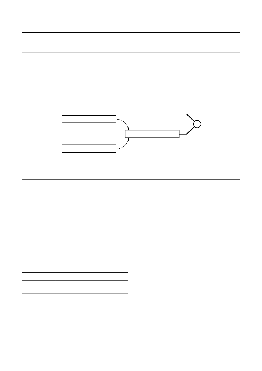
The OTP circuitry in the OM6211 contains 14 bits of data:
5 for V
LCD
calibration, 8 for V
PR
default and 1 seal bit. The
circuitry for 1-bit is called an OTP slice, thus there are
14 OTP slices.
Each OTP slice consists of 2 main parts: the OTP cell
(a non-volatile memory cell) and the shift register cell
(a flip-flop). The OTP cells are only accessible through
their shift register cells: on the one hand both reading from
and writing to the OTP cells is performed with the shift
register cells, on the other hand only the shift register cells
are visible to the rest of the circuit. The basic OTP
architecture is shown in Fig.22.
This OTP architecture enables the following operations:
1. Reading data from the OTP cells. The content of the
non-volatile OTP cells is transferred to the shift
register where it may affect the OM6211 operation
(provided it has been enabled by the `Enable OTP'
command).
2. Writing data to the OTP cells. Firstly, all 14 bits of data
are shifted into the shift register via the serial interface.
The content of the shift register is then transferred to
the OTP cells (there are some limitations related to
storing data in these cells, see Section 18.7).
3. Checking calibration without writing to the OTP cells.
Shifting data into the shift register allows the effects on
the V
LCD
voltage to be observed.
SEAL BIT
ACTION
0
possible to enter calibration mode
1
calibration mode disabled
2002 Jan 17
30
Philips Semiconductors
Product specification
48
◊
84 dot matrix LCD driver
OM6211
All OTP circuitry of the OM6211 is disabled until the
`Enable OTP' command is given. Once enabled, the
reading of data from the OTP cells is initiated by either:
∑
Exit from Power-down mode
∑
The `Refresh' command.
It should be noted that in both cases the reading operation
needs up to 5 ms to complete.
The shifting of data into the shift register is performed in a
special mode called CALMM. In the OM6211 the CALMM
mode is entered through the CALMM command. Once in
the CALMM mode the data is shifted into the shift register
via the serial interface at the rate of 1-bit per command.
After transmitting the last (14th) bit and exiting the CALMM
mode the serial interface returns to the normal mode and
all other commands can be sent. Care should be taken that
all 14 bits of data (or a multiple of 14) are transferred
before exiting the CALMM mode, otherwise the bits will be
in the wrong positions.
In the shift register the value of the seal bit is, like the
others, always zero at reset. To ensure that the security
feature works correctly, the CALMM command is disabled
until a refresh has been performed. Once the refresh is
completed, the seal bit value in the shift register is valid
and permission to enter CALMM mode can thus be
determined.
The 14 bits are shifted into the shift register in a predefined
order: firstly the 8 bits of MMOTPVOP
7
to MMOTPVOP
0
,
then the 5 bits of MMVOPCAL
4
to MMVOPCAL
0
and lastly
the seal bit. The MSB is always first, thus the first bit
shifted is MMOTPVOP
7
and the two last bits are
MMVOPCAL
0
and the seal bit.
handbook, full pagewidth
DATA TO THE CIRCUIT FOR
CONFIGURATION AND CALIBRATION
SHIFT
REGISTER
FLIP-FLOP
OTP slice
OTP CELL
SHIFT
REGISTER
SHIFT
REGISTER
DATA
INPUT
read data
from the
OTP cell
write data
to the
OTP cell
OTP CELLs
MGU289
Fig.22 Basic OTP architecture.

2002 Jan 17
31
Philips Semiconductors
Product specification
48
◊
84 dot matrix LCD driver
OM6211
18.5
Serial interface commands
These instructions are in addition to those indicated in Table 5.
Table 11 Additional instructions
INSTRUCTION
D/C
COMMAND BYTE
ACTION
DB7
DB6
DB5
DB4
DB3
DB2
DB1
DB0
Enable OTP
0
1
1
1
0
1
0
1
1
enable OTP circuitry
CALMM
0
1
1
1
0
1
1
1
1
enter CALMM mode
Load factory
default
0
1
1
1
0
1
1
0
0
load MMOTPVOP
7
to
MMOTPVOP
0
into V
PR
register
Power control
(refresh)
0
0
0
1
0
1
HVE
HVE
HVE
set HVE; force a refresh of the
shift register
18.5.1
E
NABLE
OTP
This is a special instruction for the OM6211 which enables
all included OTP circuitry. Once enabled the mode can
only be disabled via a reset.
18.5.2
CALMM
This instruction puts the device into the calibration mode.
This mode enables the shift register for loading and allows
programming of the non-volatile OTP cells to take place. If
the seal bit is set then this mode cannot be accessed and
the instruction will be ignored. Once in calibration mode all
commands are interpreted as shift register data. The mode
can only be exited by sending data with bit DB7 set to
logic 0. A reset will also clear this mode. Each shift register
data byte is preceded by D/C = 0 and has only 2 significant
bits, thus the remaining 6 bits are ignored. Bit DB7 is the
continuation bit (DB7 = 1 remain in CALMM mode,
DB7 = 0 exit CALMM mode). Bit DB0 is the data bit and its
value is shifted into the OTP shift register (on the falling
edge of SCLK).
18.5.3
L
OAD FACTORY DEFAULT
The `Load factory default' instruction is used to transfer the
contents of the OTP shift register bits MMOTPVOP
7
to
MMOTPVOP
0
into the normal working register of V
PR
;
see Fig.21. This is opposite to the calibration register
MMVOPCAL
4
to MMVOPCAL
0
which is active
immediately after a refresh.
18.5.4
R
EFRESH
The action of the `Refresh' instruction is to force the OTP
shift register to re-load from the non-volatile OTP cells.
This instruction takes up to 5 ms to complete.
During this time all other instructions may be sent,
however, instructions requiring the output of the shift
register (`Load factory default') should be avoided as the
register contents may not be valid.
In the OM6211 the `Refresh' instruction is associated to
the `Set HVE' instruction so that the shift register is
automatically refreshed every time the high voltage
generator is enabled or disabled. It should be noted
however, that if this instruction is sent while in Power-down
mode, then the HVE bit is updated but the refreshing is
ignored.
18.6
Example of filling the shift register
An example sequence of commands and data is shown in
Table 12. In this example the shift register is filled with the
following data: MMVOPCAL =
-
4 (11100B),
MMOTPVOP = 19 (00010011B) and the seal bit is 0.
It is assumed that the OM6211 has just been reset. After
transmitting the last bit the OM6211 can exit or remain in
CALMM mode (see step 18). It should be noted that while
in CALMM mode the interface does not recognize
commands in the normal sense.
After this sequence has been applied it is possible to
observe the impact of the data shifted in. This sequence is,
however, not useful for OTP programming because the
number of bits with the value `1' is greater than that
allowed for programming (see Section 18.7). Figure 23
shows the shift register after this action.

2002 Jan 17
32
Philips Semiconductors
Product specification
48
◊
84 dot matrix LCD driver
OM6211
Table 12 Example sequence for filling the shift register; note 1
Notes
1. X = don't care.
2. The data for the bits is not in the correct shift register position until all bits have been sent.
STEP
D/C
COMMAND BYTE
ACTION
DB7
DB6
DB5
DB4
DB3
DB2
DB1
DB0
1
0
1
1
1
0
1
0
1
1
send enable OTP command
2
0
1
0
1
0
1
1
1
1
exit Power-down (e.g. DON = 1)
3
wait 5 ms for refresh to take effect.
4
0
1
1
1
0
1
1
1
1
enter CALMM mode
5
0
1
X
X
X
X
X
X
0
shift in data; MMOTPVOP
7
is first bit; note 2
6
0
1
X
X
X
X
X
X
0
MMOTPVOP
6
7
0
1
X
X
X
X
X
X
0
MMOTPVOP
5
8
0
1
X
X
X
X
X
X
1
MMOTPVOP
4
9
0
1
X
X
X
X
X
X
0
MMOTPVOP
3
10
0
1
X
X
X
X
X
X
0
MMOTPVOP
2
11
0
1
X
X
X
X
X
X
1
MMOTPVOP
1
12
0
1
X
X
X
X
X
X
1
MMOTPVOP
0
13
0
1
X
X
X
X
X
X
1
MMVOPCAL
4
14
0
1
X
X
X
X
X
X
1
MMVOPCAL
3
15
0
1
X
X
X
X
X
X
1
MMVOPCAL
2
16
0
1
X
X
X
X
X
X
0
MMVOPCAL
1
17
0
1
X
X
X
X
X
X
0
MMVOPCAL
0
18
0
0
X
X
X
X
X
X
0
seal bit; exit CALMM mode
An alternative ending could be to stay in CALMM mode
18
0
1
X
X
X
X
X
X
0
seal bit; remain in CALMM mode
handbook, full pagewidth
MSB
LSB
shifting
direction
0
MGU290
MMVOPCAL[4:0]
SEAL
BIT = 0
0
1
1
1
MSB
LSB
1
MMOTPVOP[7:0]
OTP SHIFT REGISTER
1
0
0
0
0
0
1
Fig.23 Shift register contents after example sequence of Table 12.

2002 Jan 17
33
Philips Semiconductors
Product specification
48
◊
84 dot matrix LCD driver
OM6211
18.7
Programming flow
Programming is achieved whilst in CALMM mode and with
the application of the programming voltages. As
mentioned previously, the data for programming the OTP
cell is contained in the corresponding shift register cell.
The shift register cell must be loaded with a logic 1 in order
to program the corresponding OTP cell. If the shift register
cell contains a logic 0, then no action will take place when
the programming voltages are applied.
Once programmed, an OTP cell can not be
un-programmed. An already programmed cell, that is an
OTP cell containing a logic 1, must not be re-programmed.
The order for programming cells is not significant.
However, it is recommended that the seal bit is
programmed last.
Once this bit has been programmed it will not be possible
to re-enter the CALMM mode.
During programming a substantial current flows in the
V
LCDIN
pin. For this reason it is recommended to program
only one OTP cell at a time. This is achieved by filling all
but one shift register cells with logic 0. It should be noted
that the programming specification refers to the voltages at
the chip pins, contact resistance must therefore be
considered by the user.
An example sequence of commands and data for OTP
programming is shown in Table 13.
It is assumed that the OM6211 has just been reset.
Table 13 Example sequence for OTP programming; note 1
Note
1. X = don't care.
STEP
D/C
COMMAND BYTE
ACTION
DB7
DB6
DB5
DB4
DB3
DB2
DB1
DB0
1
0
1
1
1
0
1
0
1
1
send Enable OTP command
2
0
1
0
1
0
1
1
1
1
exit Power-down (e.g. DON = 1)
3
wait 5 ms for refresh to take effect
4
0
1
0
1
0
1
1
1
0
re-enter Power-down (DON = 0)
5
0
1
1
1
0
1
1
1
1
enter CALMM mode
6
0
1
X
X
X
X
X
X
0
shift in data. MMOTPVOP
7
7
0
1
X
X
X
X
X
X
0
MMOTPVOP
6
8
0
1
X
X
X
X
X
X
0
MMOTPVOP
5
9
0
1
X
X
X
X
X
X
1
MMOTPVOP
4
(the only bit with the value 1)
10
0
1
X
X
X
X
X
X
0
MMOTPVOP
3
11
0
1
X
X
X
X
X
X
0
MMOTPVOP
2
12
0
1
X
X
X
X
X
X
0
MMOTPVOP
1
13
0
1
X
X
X
X
X
X
0
MMOTPVOP
0
14
0
1
X
X
X
X
X
X
0
MMVOPCAL
4
15
0
1
X
X
X
X
X
X
0
MMVOPCAL
3
16
0
1
X
X
X
X
X
X
0
MMVOPCAL
2
17
0
1
X
X
X
X
X
X
0
MMVOPCAL
1
18
0
1
X
X
X
X
X
X
0
MMVOPCAL
0
19
0
1
X
X
X
X
X
X
0
seal bit; remain in CALMM mode
20
apply programming voltage at pins T6 and
V
LCDIN
according to Section 18.8
Repeat steps 6 to 20 for each bit that should be programmed to 1
21
apply external reset

2002 Jan 17
34
Philips Semiconductors
Product specification
48
◊
84 dot matrix LCD driver
OM6211
18.8
Programming specification
Table 14 Programming specification; see Fig.24
Notes
1. The voltage drop across the I
TO
track and zebra connector must be taken into account to guarantee sufficient voltage
at the chip pins.
2. The maximum voltage must not be exceeded even for a short period of time. Therefore care must be taken when
applying programming waveforms to avoid overshoot.
3. The Power-down mode (DON = 0 and DAL = 1) and CALMM mode must be active while the V
LCDIN
pin is being
driven.
SYMBOL
PARAMETER
CONDITION
MIN.
TYP.
MAX.
UNIT
V
T6
voltage applied to T6 pin relative to V
SS1
programming active;
notes 1 and 2
11
11.5
12
V
programming inactive;
notes 1 and 2
V
SS
-
0.2 0
0.2
V
V
LCDIN
voltage applied to V
LCDIN
pin relative to
V
SS1
programming active;
notes 1 and 3
9
9.5
10
V
programming inactive;
notes 1 and 3
-
0.2
0
+4.5
V
I
LCDIN
current drawn by V
LCDIN
during
programming
when programming a
single bit to logic 1
-
850
1000
µ
A
I
T6
current drawn by V
T6
during
programming
-
100
200
µ
A
T
amb(prog)
ambient temperature during
programming
0
25
40
∞
C
t
su;SCLK
set-up of internal data after last clock
1
-
-
µ
s
t
h;SCLK
hold of internal data before next clock
1
-
-
µ
s
t
su;T6
set-up of V
T6
prior to programming
1
-
10
ms
t
h;T6
hold of V
T6
after programming
1
-
10
ms
t
W
pulse width of programming voltage
100
120
200
ms
handbook, full pagewidth
SCLK
tsw;SCLK
tsw;T6
th;T6
tw
MGU291
VT6
VLCDIN
th;SCLK
Fig.24 Programming waveforms.
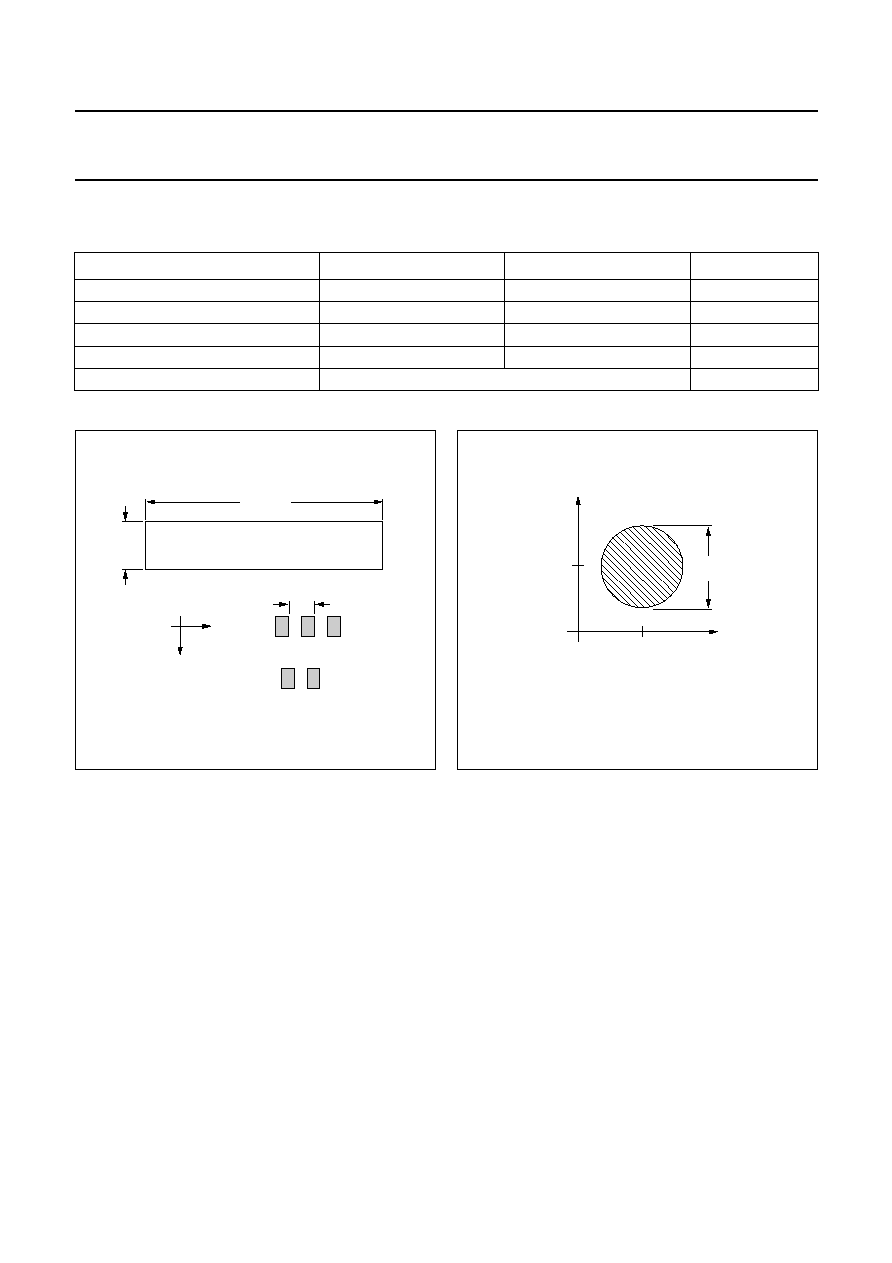
2002 Jan 17
35
Philips Semiconductors
Product specification
48
◊
84 dot matrix LCD driver
OM6211
19 BONDING PAD LOCATIONS
Table 15 Bonding pad information
PAD
ROWS AND COLS SIDE
INTERFACE SIDE
UNIT
Pad pitch
minimum 60
minimum 70
µ
m
Pad size (aluminium)
50
◊
90
60
◊
100
µ
m
CBB opening
26
◊
66
36
◊
76
µ
m
Bump dimensions
40
◊
80
◊
17.5 (
±
5)
50
◊
90
◊
17.5 (
±
5)
µ
m
Wafer thickness (excluding bumps)
381 (
±
25)
µ
m
handbook, halfpage
MGU292
9.46 mm
pitch
1.91
mm
y
x
OM6211
Fig.25 Chip size and pad pitch.
MGT855
handbook, halfpage
x
center
y
center
100
µ
m
Fig.26 Shape of alignment mark.
2002 Jan 17
36
Philips Semiconductors
Product specification
48
◊
84 dot matrix LCD driver
OM6211
Table 16 Bonding pad location
All x and y co-ordinates are referenced to the centre of
the chip (dimensions in
µ
m; see Fig.27).
SYMBOL
PAD
COORDINATES
x
y
Dummy
1
-
835
+4630
Alignment mark
2
-
825
+4527.5
V
OS4
3
-
835
+4425
V
OS3
4
-
835
+4215
V
OS2
5
-
835
+4005
V
OS1
6
-
835
+3795
V
OS0
7
-
835
+3585
T6
8
-
835
+3375
T6
9
-
835
+3305
T6
10
-
835
+3235
T6
11
-
835
+3165
Dummy
12
-
835
+3095
Dummy
13
-
835
+3025
Dummy
14
-
835
+2955
Dummy
15
-
835
+2885
RES
16
-
835
+2395
T5
17
-
835
+2185
T4
18
-
835
+1975
T3
19
-
835
+1765
T2
20
-
835
+1555
T1
21
-
835
+1345
SCE
22
-
835
+1135
V
SS2
23
-
835
+1065
V
SS2
24
-
835
+995
V
SS2
25
-
835
+925
V
SS2
26
-
835
+855
V
SS2
27
-
835
+785
V
SS2
28
-
835
+715
V
SS2
29
-
835
+645
V
SS2
30
-
835
+575
V
SS1
31
-
835
+505
V
SS1
32
-
835
+435
V
SS1
33
-
835
+365
V
SS1
34
-
835
+295
V
SS1
35
-
835
+225
V
SS1
36
-
835
+155
V
SS1
37
-
835
+85
V
SS1
38
-
835
+15
Dummy
39
-
835
-
405
OSC
40
-
835
-
825
SDOUT
41
-
835
-
1035
SDIN
42
-
835
-
1245
SCLK
43
-
835
-
1455
ID4
44
-
835
-
1665
ID3
45
-
835
-
1875
MX
46
-
835
-
2085
V
DD1
47
-
835
-
2155
V
DD1
48
-
835
-
2225
V
DD1
49
-
835
-
2295
V
DD1
50
-
835
-
2365
V
DD1
51
-
835
-
2435
V
DD1
52
-
835
-
2505
V
DD2
53
-
835
-
2575
V
DD2
54
-
835
-
2645
V
DD2
55
-
835
-
2715
V
DD2
56
-
835
-
2785
V
DD2
57
-
835
-
2855
V
DD2
58
-
835
-
2925
V
DD2
59
-
835
-
2995
V
DD2
60
-
835
-
3065
V
DD3
61
-
835
-
3135
V
DD3
62
-
835
-
3205
V
DD3
63
-
835
-
3275
V
DD3
64
-
835
-
3345
V
LCDSENSE
65
-
835
-
3415
V
LCDOUT
66
-
835
-
3485
V
LCDOUT
67
-
835
-
3555
V
LCDOUT
68
-
835
-
3625
V
LCDOUT
69
-
835
-
3695
V
LCDOUT
70
-
835
-
3765
V
LCDOUT
71
-
835
-
3835
V
LCDOUT
72
-
835
-
3905
V
LCDIN
73
-
835
-
3975
V
LCDIN
74
-
835
-
4045
V
LCDIN
75
-
835
-
4115
V
LCDIN
76
-
835
-
4185
SYMBOL
PAD
COORDINATES
x
y

2002 Jan 17
37
Philips Semiconductors
Product specification
48
◊
84 dot matrix LCD driver
OM6211
V
LCDIN
77
-
835
-
4255
V
LCDIN
78
-
835
-
4325
Dummy
79
-
835
-
4395
Alignment mark
80
-
825
-
4500
Dummy
81
-
835
-
4605
Dummy
82
+840
-
4590
Dummy
83
+840
-
4530
Dummy
84
+840
-
4470
Dummy
85
+840
-
4410
Dummy
86
+840
-
4350
Dummy
87
+840
-
4290
Dummy
88
+840
-
4230
ROW 0
89
+840
-
4050
ROW 1
90
+840
-
3990
ROW 2
91
+840
-
3930
ROW 3
92
+840
-
3870
ROW 4
93
+840
-
3810
ROW 5
94
+840
-
3750
ROW 6
95
+840
-
3690
ROW 7
96
+840
-
3630
ROW 8
97
+840
-
3570
ROW 9
98
+840
-
3510
ROW 10
99
+840
-
3450
ROW 11
100
+840
-
3390
ROW 12
101
+840
-
3330
ROW 13
102
+840
-
3270
ROW 14
103
+840
-
3210
ROW 15
104
+840
-
3150
ROW 16
105
+840
-
3090
ROW 17
106
+840
-
3030
ROW 18
107
+840
-
2970
ROW 19
108
+840
-
2910
ROW 20
109
+840
-
2850
ROW 21
110
+840
-
2790
ROW 22
111
+840
-
2730
ROW 23
112
+840
-
2670
COL 0
113
+840
-
2490
COL 1
114
+840
-
2430
COL 2
115
+840
-
2370
SYMBOL
PAD
COORDINATES
x
y
COL 3
116
+840
-
2310
COL 4
117
+840
-
2250
COL 5
118
+840
-
2190
COL 6
119
+840
-
2130
COL 7
120
+840
-
2070
COL 8
121
+840
-
2010
COL 9
122
+840
-
1950
COL 10
123
+840
-
1890
COL 11
124
+840
-
1830
COL 12
125
+840
-
1770
COL 13
126
+840
-
1710
COL 14
127
+840
-
1650
COL 15
128
+840
-
1590
COL 16
129
+840
-
1530
COL 17
130
+840
-
1470
COL 18
131
+840
-
1410
COL 19
132
+840
-
1350
COL 20
133
+840
-
1290
COL 21
134
+840
-
1230
COL 22
135
+840
-
1170
COL 23
136
+840
-
1110
COL 24
137
+840
-
1050
COL 25
138
+840
-
990
COL 26
139
+840
-
930
COL 27
140
+840
-
870
COL 28
141
+840
-
690
COL 29
142
+840
-
630
COL 30
143
+840
-
570
COL 31
144
+840
-
510
COL 32
145
+840
-
450
COL 33
146
+840
-
390
COL 34
147
+840
-
330
COL 35
148
+840
-
270
COL 36
149
+840
-
210
COL 37
150
+840
-
150
COL 38
151
+840
-
90
COL 39
152
+840
-
30
COL 40
153
+840
+30
COL 41
154
+840
+90
SYMBOL
PAD
COORDINATES
x
y

2002 Jan 17
38
Philips Semiconductors
Product specification
48
◊
84 dot matrix LCD driver
OM6211
COL 42
155
+840
+150
COL 43
156
+840
+210
COL 44
157
+840
+270
COL 45
158
+840
+330
COL 46
159
+840
+390
COL 47
160
+840
+450
COL 48
161
+840
+510
COL 49
162
+840
+570
COL 50
163
+840
+630
COL 51
164
+840
+690
COL 52
165
+840
+750
COL 53
166
+840
+810
COL 54
167
+840
+870
COL 55
168
+840
+930
COL 56
169
+840
+1110
COL 57
170
+840
+1170
COL 58
171
+840
+1230
COL 59
172
+840
+1290
COL 60
173
+840
+1350
COL 61
174
+840
+1410
COL 62
175
+840
+1470
COL 63
176
+840
+1530
COL 64
177
+840
+1590
COL 65
178
+840
+1650
COL 66
179
+840
+1710
COL 67
180
+840
+1770
COL 68
181
+840
+1830
COL 69
182
+840
+1890
COL 70
183
+840
+1950
COL 71
184
+840
+2010
COL 72
185
+840
+2070
COL 73
186
+840
+2130
COL 74
187
+840
+2190
COL 75
188
+840
+2250
COL 76
189
+840
+2310
COL 77
190
+840
+2370
COL 78
191
+840
+2430
COL 79
192
+840
+2490
COL 80
193
+840
+2550
SYMBOL
PAD
COORDINATES
x
y
COL 81
194
+840
+2610
COL 82
195
+840
+2670
COL 83
196
+840
+2730
ROW 47
197
+840
+2910
ROW 46
198
+840
+2970
ROW 45
199
+840
+3030
ROW 44
200
+840
+3090
ROW 43
201
+840
+3150
ROW 42
202
+840
+3210
ROW 41
203
+840
+3270
ROW 40
204
+840
+3330
ROW 39
205
+840
+3390
ROW 38
206
+840
+3450
ROW 37
207
+840
+3510
ROW 36
208
+840
+3570
ROW 35
209
+840
+3630
ROW 34
210
+840
+3690
ROW 33
211
+840
+3750
ROW 32
212
+840
+3810
ROW 31
213
+840
+3870
ROW 30
214
+840
+3930
ROW 29
215
+840
+3990
ROW 28
216
+840
+4050
ROW 27
217
+840
+4110
ROW 26
218
+840
+4170
ROW 25
219
+840
+4230
ROW 24
220
+840
+4290
Dummy
221
+840
+4350
Dummy
222
+840
+4410
Dummy
223
+840
+4470
Dummy
224
+840
+4530
Dummy
225
+840
+4590
SYMBOL
PAD
COORDINATES
x
y
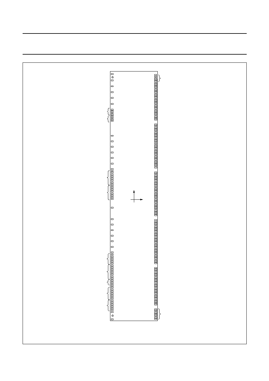
2002 Jan 17
39
Philips Semiconductors
Product specification
48
◊
84 dot matrix LCD driver
OM6211
MGU293
dummy pad
dummy pad
dummy pad
COL 0
ROW 0
dummy pad
dummy pad
dummy pad
T6
alignment mark
alignment mark
OM6211-1
VOS3
VOS2
VOS4
VOS1
VOS0
.
.
.
ROW 23
.
.
.
COL 27
.
.
.
.
.
.
COL 28
COL 55
.
.
.
.
.
.
COL 56
COL 83
.
.
.
.
.
.
ROW 24
ROW 47
.
.
.
.
.
.
VSS1
VSS2
VLCDSENSE
VLCDOUT
VDD1
VDD2
VDD3
OSC
dummy pad
SCE
RES
T5
T4
T3
T2
T1
SDOUT
SDIN
ID3
ID4
SCLK
MX
VLCDIN
x
y
0, 0
Fig.27 Pad locations.
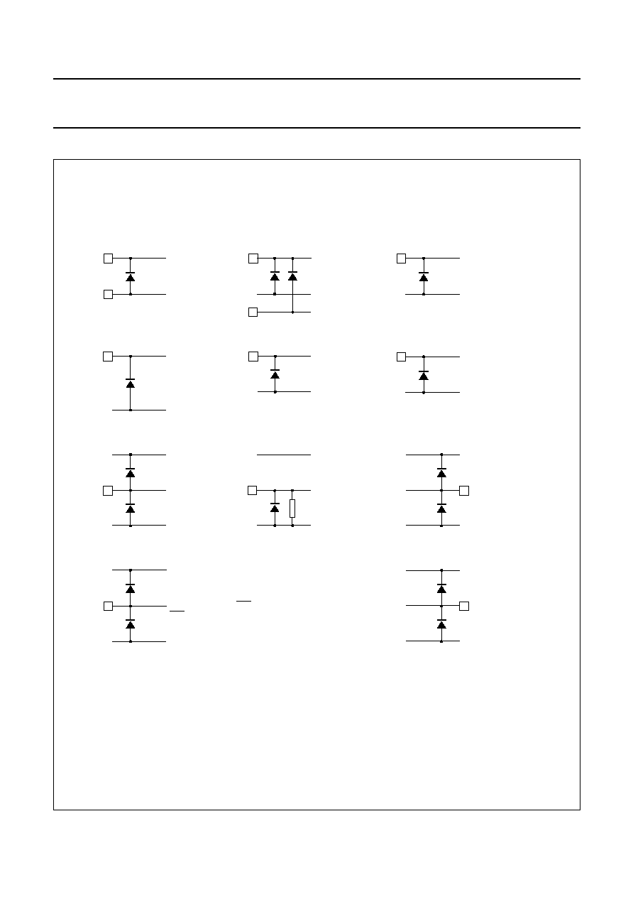
2002 Jan 17
40
Philips Semiconductors
Product specification
48
◊
84 dot matrix LCD driver
OM6211
20 DEVICE PROTECTION DIAGRAM
handbook, full pagewidth
MGU294
VDD1
VDD1
VSS1
VSS2
VSS1
VOS[4:0]
VSS1
VSS1
VDD1
OSC, SDIN, SCLK, SCE,
RES, T4, T5, MX, ID3, ID4
VLCDOUT
VSS1
VLCDIN(SUPPLY),
VLCDSENSE
VLCDIN
VSS1
VDD2
VSS1
VSS2
VDD1
VSS1
VSS1
T6
VDD3
VSS1
VLCDIN
VSS1
SDOUT, T1, T2, T3
COL0 to COL83
ROW0 to ROW47
Fig.28 Device protection diagram.
The conditions for continuity tests are as follows:
Maximum forward current = 5 mA; Maximum reverse voltage = 5 V.

2002 Jan 17
41
Philips Semiconductors
Product specification
48
◊
84 dot matrix LCD driver
OM6211
21 TRAY INFORMATION
handbook, full pagewidth
MGU295
D
F
E
x
y
A
1,1
x,1
2,1
1,2
1,3
1,y
x,y
2,2
3,1
C
B
Fig.29 Tray details.
Table 17 Tray dimensions
handbook, halfpage
OM6211-1
MGU296
Fig.30 Tray alignment.
The orientation of the IC in a pocket is indicated by the position of the
IC type name on the die surface with respect to the chamfer on the
upper left corner of the tray. Refer to the bonding pad location
diagram for the orientation and position of the type name on the
surface.
DIMENSION
DESCRIPTION
VALUE
A
pocket pitch x direction
13.76 mm
B
pocket pitch y direction
4.45 mm
C
pocket width x direction 9.56 mm
D
pocket width y direction 2.00 mm
E
tray width x direction
50.80 mm
F
tray width y direction
50.80 mm
x
number of pockets in
x direction
3
y
number of pockets in
y direction
10

2002 Jan 17
42
Philips Semiconductors
Product specification
48
◊
84 dot matrix LCD driver
OM6211
22 APPLICATION NOTES
When reading the VM bit in the OM6211 two problems
have been observed: corrupted format and VM bit
toggling.
22.1
Corrupted format
The read-out of the VM bit has a special format, 11110000
for VM = 1 and 00001111 for VM = 0. However,
sometimes a wrong format of the read-out byte can be
observed; the first or the fifth or the eighth bit appears to
be wrong. There are two reasons for this behaviour. When
the first bit happens to be read out at the end of a frame
then it is possible that the first bit belongs to the old VM
value and the 7 following bits belong to the new VM value.
Such behaviour is possible for the first bit only. The second
reason is the violation of the OM6211 timing, if the timing
parameters t
2
and t
3
(see Fig.17) are violated, then it
results in reading a wrong value for the first, the fifth or the
eighth bit. Thus, to prevent any problems with the wrong
format of the read-out byte, these bits should always be
ignored.
22.2
VM bit toggling
Under certain conditions it can happen that the result of
reading VM is 0 even if the generated V
LCD
voltage is
correct (VM bit toggles). It is therefore recommended to
repeat the VM read command several times according to
the algorithm described below. This algorithm is based on
the observation that a single reading of VM = 1 (after
numerous readings of VM = 0) is enough to ensure that
the charge pump operation is correct. One possible
method which gives minimum measurement duration is
shown in Fig.31 and described in detail below:
∑
Perform initialization with Enable OTP and set the
operational parameters (V
PR
= 159, S = 10, BS = 101,
TC = 1, E = 0 and MY = 0) this results in a slightly higher
V
LCD
voltage than for normal operation (V
LCD
= 8.732 V
at T
amb
= 27
∞
C)
∑
Select DAL = 1 and DON = 1 (for all pixels on)
∑
After setting HVE = 1 start a loop of a continuous VM
reading (for example, every 1 ms), at first occurrence of
reading VM = 1 interrupt the loop and accept VM = 1
∑
When the reading is always VM = 0, stop the loop after
a certain time and accept VM = 0. This loop time limit
should be chosen sufficiently long, e.g. 85 ms. Given
that the uncertainty is much less then 0.1%, much less
then 1 ppm is expected to be read out wrong.
For the loop time limit a value of not less than 85 ms is
suggested. It should be noted that the value of 45 ms
specified in Section 11.2.2 means that after at least 45 ms
the VM measurement is possible. In practice it can be
expected that VM is valid earlier than 45 ms. Therefore the
proposed algorithm results in an optimization of the 45 ms
wait time needed to charge the external V
LCD
capacitor.
So the selected loop time limit of 85 ms consists of 45 ms
wait time and an additional 40 ms of measurement time.
The loop time limit of 85 ms will ensure that even if the first
VM = 1 value for any reason should be missed, there is
always the possibility to hit the next VM = 1 value (note
that the internal VM measurement is made once per
12.5 ms). However, the expectation is that the average
running time of the loop will be less than 45 ms.
There is another possibility for optimization: during the wait
time of the loop (1 ms) other tasks can be performed.
Furthermore the first part of the 45 ms wait time, just after
setting HVE = 1, may also be used for other tasks. For
instance when the first 20 ms are reserved for those tasks,
then the corresponding loop time limit would be 65 ms and
the expected average loop time would be less than 25 ms.
After the VM test is completed the V
PR
can be set to the
desired value (e.g. V
PR
= 137) without the charge pump
being switched off.
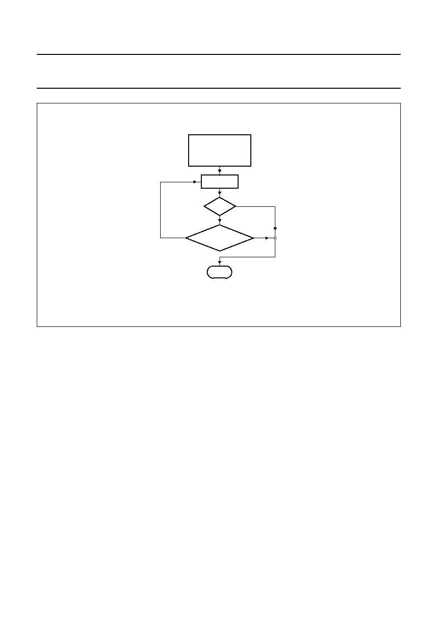
2002 Jan 17
43
Philips Semiconductors
Product specification
48
◊
84 dot matrix LCD driver
OM6211
handbook, halfpage
initialization
HVE = 1
loop_time_limit = 85 ms
reset time_counter
read VM bit
yes
yes
wait 1 ms
no
no
VM = 1 ?
end
MGU521
time_counter <
loop_time_limit?
Fig.31 Algorithm of reliable and fast read-out of the VM bit.

2002 Jan 17
44
Philips Semiconductors
Product specification
48
◊
84 dot matrix LCD driver
OM6211
23 DATA SHEET STATUS
Notes
1. Please consult the most recently issued data sheet before initiating or completing a design.
2. The product status of the device(s) described in this data sheet may have changed since this data sheet was
published. The latest information is available on the Internet at URL http://www.semiconductors.philips.com.
DATA SHEET STATUS
(1)
PRODUCT
STATUS
(2)
DEFINITIONS
Objective data
Development
This data sheet contains data from the objective specification for product
development. Philips Semiconductors reserves the right to change the
specification in any manner without notice.
Preliminary data
Qualification
This data sheet contains data from the preliminary specification.
Supplementary data will be published at a later date. Philips
Semiconductors reserves the right to change the specification without
notice, in order to improve the design and supply the best possible
product.
Product data
Production
This data sheet contains data from the product specification. Philips
Semiconductors reserves the right to make changes at any time in order
to improve the design, manufacturing and supply. Changes will be
communicated according to the Customer Product/Process Change
Notification (CPCN) procedure SNW-SQ-650A.
24 DEFINITIONS
Short-form specification
The data in a short-form
specification is extracted from a full data sheet with the
same type number and title. For detailed information see
the relevant data sheet or data handbook.
Limiting values definition
Limiting values given are in
accordance with the Absolute Maximum Rating System
(IEC 60134). Stress above one or more of the limiting
values may cause permanent damage to the device.
These are stress ratings only and operation of the device
at these or at any other conditions above those given in the
Characteristics sections of the specification is not implied.
Exposure to limiting values for extended periods may
affect device reliability.
Application information
Applications that are
described herein for any of these products are for
illustrative purposes only. Philips Semiconductors make
no representation or warranty that such applications will be
suitable for the specified use without further testing or
modification.
25 DISCLAIMERS
Life support applications
These products are not
designed for use in life support appliances, devices, or
systems where malfunction of these products can
reasonably be expected to result in personal injury. Philips
Semiconductors customers using or selling these products
for use in such applications do so at their own risk and
agree to fully indemnify Philips Semiconductors for any
damages resulting from such application.
Right to make changes
Philips Semiconductors
reserves the right to make changes, without notice, in the
products, including circuits, standard cells, and/or
software, described or contained herein in order to
improve design and/or performance. Philips
Semiconductors assumes no responsibility or liability for
the use of any of these products, conveys no licence or title
under any patent, copyright, or mask work right to these
products, and makes no representations or warranties that
these products are free from patent, copyright, or mask
work right infringement, unless otherwise specified.

2002 Jan 17
45
Philips Semiconductors
Product specification
48
◊
84 dot matrix LCD driver
OM6211
NOTES

2002 Jan 17
46
Philips Semiconductors
Product specification
48
◊
84 dot matrix LCD driver
OM6211
NOTES

2002 Jan 17
47
Philips Semiconductors
Product specification
48
◊
84 dot matrix LCD driver
OM6211
NOTES

© Koninklijke Philips Electronics N.V. 2002
SCA74
All rights are reserved. Reproduction in whole or in part is prohibited without the prior written consent of the copyright owner.
The information presented in this document does not form part of any quotation or contract, is believed to be accurate and reliable and may be changed
without notice. No liability will be accepted by the publisher for any consequence of its use. Publication thereof does not convey nor imply any license
under patent- or other industrial or intellectual property rights.
Philips Semiconductors ≠ a worldwide company
Contact information
For additional information please visit http://www.semiconductors.philips.com.
Fax: +31 40 27 24825
For sales offices addresses send e-mail to: sales.addresses@www.semiconductors.philips.com.
Printed in The Netherlands
403512/01/pp
48
Date of release:
2002 Jan 17
Document order number:
9397 750 07744