
Philips
Semiconductors
XA-G3
XA 16-bit microcontroller family
32K/512 OTP/ROM/ROMless, watchdog, 2 UARTs
Product specification
Supersedes data of 1998 Aug 14
IC25 Data Handbook
1999 Apr 07
INTEGRATED CIRCUITS

Philips Semiconductors
Product specification
XA-G3
XA 16-bit microcontroller family
32K/512 OTP/ROM/ROMless, watchdog, 2 UARTs
2
1999 Apr 07
853-2052 21197
FAMILY DESCRIPTION
The Philips Semiconductors XA (eXtended Architecture) family of
16-bit single-chip microcontrollers is powerful enough to easily
handle the requirements of high performance embedded
applications, yet inexpensive enough to compete in the market for
high-volume, low-cost applications.
The XA family provides an upward compatibility path for 80C51
users who need higher performance and 64k or more of program
memory. Existing 80C51 code can also easily be translated to run
on XA microcontrollers.
The performance of the XA architecture supports the
comprehensive bit-oriented operations of the 80C51 while
incorporating support for multi-tasking operating systems and
high-level languages such as C. The speed of the XA architecture,
at 10 to 100 times that of the 80C51, gives designers an easy path
to truly high performance embedded control.
The XA architecture supports:
�
Upward compatibility with the 80C51 architecture
�
16-bit fully static CPU with a 24-bit program and data address
range
�
Eight 16-bit CPU registers each capable of performing all
arithmetic and logic operations as well as acting as memory
pointers. Operations may also be performed directly to memory.
�
Both 8-bit and 16-bit CPU registers, each capable of performing
all arithmetic and logic operations.
�
An enhanced instruction set that includes bit intensive logic
operations and fast signed or unsigned 16
�
16 multiply and
32 / 16 divide
�
Instruction set tailored for high level language support
�
Multi-tasking and real-time executives that include up to 32
vectored interrupts, 16 software traps, segmented data memory,
and banked registers to support context switching
�
Low power operation, which is intrinsic to the XA architecture,
includes power-down and idle modes.
More detailed information on the core is available in the XA User
Guide.
SPECIFIC FEATURES OF THE XA-G3
�
20-bit address range, 1 megabyte each program and data space.
(Note that the XA architecture supports up to 24 bit addresses.)
�
2.7V to 5.5V operation
�
32K bytes on-chip EPROM/ROM program memory =
XA-G37/XA-G33
�
512 bytes of on-chip data RAM
�
Three counter/timers with enhanced features
(equivalent to 80C51 T0, T1, and T2)
�
Watchdog timer
�
Two enhanced UARTs
�
Four 8-bit I/O ports with 4 programmable output configurations
�
44-pin PLCC and 44-pin LQFP packages
ORDERING INFORMATION
ROMless
ROM
EPROM
1
TEMPERATURE RANGE
�
C AND PACKAGE
FREQ
(MHz)
DRAWING
NUMBER
P51XAG30KB BD
P51XAG33KB BD
PXAG37KB BD
OTP
0 to +70, Plastic Low Profile Quad Flat Pkg.
30
SOT389�1
P51XAG30KB A
P51XAG33KB A
PXAG37KB A
OTP
0 to +70, Plastic Leaded Chip Carrier
30
SOT187�2
P51XAG30KF BD
P51XAG33KF BD
PXAG37KF BD
OTP
�40 to +85, Plastic Low Profile Quad Flat Pkg.
30
SOT389�1
P51XAG30KF A
P51XAG33KF A
PXAG37KF A
OTP
�40 to +85, Plastic Leaded Chip Carrier
30
SOT187�2
NOTE:
1. OTP = One Time Programmable EPROM. UV = Erasable EPROM.
Philips Semiconductors
Product specification
XA-G3
XA 16-bit microcontroller family
32K/512 OTP/ROM/ROMless, watchdog, 2 UARTs
1999 Apr 07
3
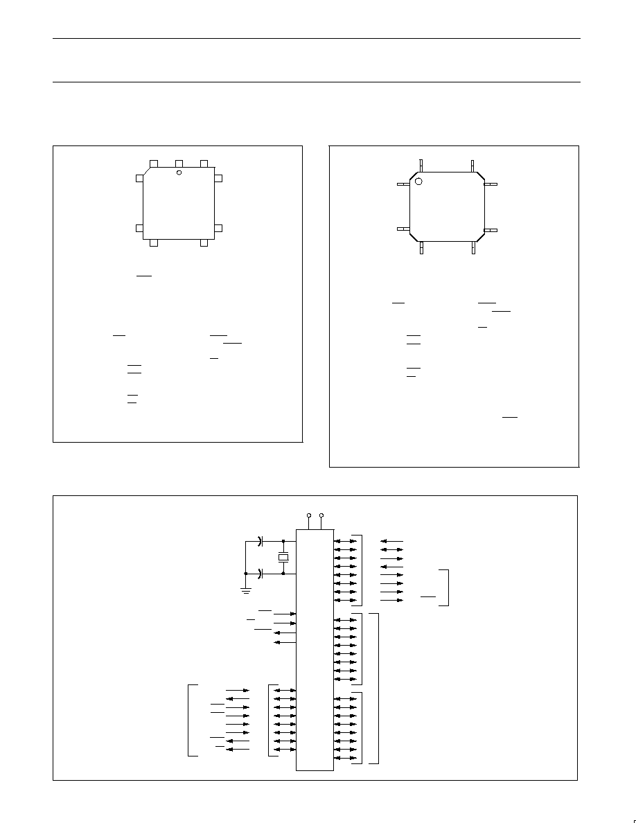
PIN CONFIGURATIONS
44-Pin PLCC Package
PLCC
6
1
40
7
17
39
29
18
28
Pin
Function
1
V
SS
2
P1.0/A0/WRH
3
P1.1/A1
4
P1.2/A2
5
P1.3/A3
6
P1.4/RxD1
7
P1.5/TxD1
8
P1.6/T2
9
P1.7/T2EX
10
RST
11
P3.0/RxD0
12
NC
13
P3.1/TxD0
14
P3.2/INT0
15
P3.3/INT1
16
P3.4/T0
17
P3.5/T1/BUSW
18
P3.6/WRL
19
P3.7/RD
20
XTAL2
21
XTAL1
22
V
SS
Pin
Function
23
V
DD
24
P2.0/A12D8
25
P2.1/A13D9
26
P2.2/A14D10
27
P2.3/A15D11
28
P2.4/A16D12
29
P2.5/A17D13
30
P2.6/A18D14
31
P2.7/A19D15
32
PSEN
33
ALE/PROG
34
NC
35
EA/V
PP
/WAIT
36
P0.7/A11D7
37
P0.6/A10D6
38
P0.5/A9D5
39
P0.4/A8D4
40
P0.3/A7D3
41
P0.2/A6D2
42
P0.1/A5D1
43
P0.0/A4D0
44
V
DD
SU00525
44-Pin LQFP Package
LQFP
44
34
1
11
33
23
12
22
Pin
Function
1
P1.5/TxD1
2
P1.6/T2
3
P1.7/T2EX
4
RST
5
P3.0/RxD0
6
NC
7
P3.1/TxD0
8
P3.2/INT0
9
P3.3/INT1
10
P3.4/T0
11
P3.5/T1/BUSW
12
P3.6/WRL
13
P3.7/RD
14
XTAL2
15
XTAL1
16
V
SS
17
V
DD
18
P2.0/A12D8
19
P2.1/A13D9
20
P2.2/A14D10
21
P2.3/A15D11
22
P2.4/A16/D12
Pin
Function
23
P2.5/A17D13
24
P2.6/A18D14
25
P2.7/A19D15
26
PSEN
27
ALE/PROG
28
NC
29
EA/V
PP
/WAIT
30
P0.7/A11D7
31
P0.6/A10D6
32
P0.5/A9D5
33
P0.4/A8D4
34
P0.3/A7D3
35
P0.2/A6D2
36
P0.1/A5D1
37
P0.0/A4D0
38
V
DD
39
V
SS
40
P1.0/A0/WRH
41
P1.1/A1
42
P1.2/A2
43
P1.3/A3
44
P1.4/RxD1
SU00580
LOGIC SYMBOL
V
DD
V
SS
XTAL1
XTAL2
RST
EA/WAIT
T2*
T2EX*
A3
A2
SU00526
A1
A0/WRH
POR
T
1
POR
T
2
PSEN
ALE
POR
T
0
ADDRESS AND
DA
T
A
BUS
ADDRESS
BUS
POR
T
3
T0
T1/BUSW
WRL
RD
RxD0
TxD0
INT0
INT1
AL
TERNA
TE FUNCTIONS
*
NOT AVAILABLE ON 40-PIN DIP PACKAGE
T
X
D1
R
X
D1
Philips Semiconductors
Product specification
XA-G3
XA 16-bit microcontroller family
32K/512 OTP/ROM/ROMless, watchdog, 2 UARTs
1999 Apr 07
4
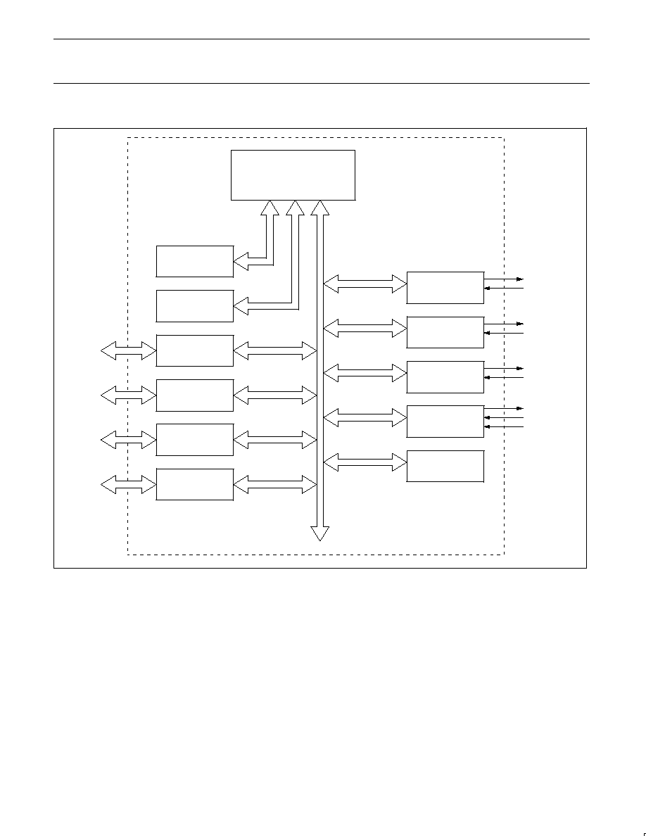
BLOCK DIAGRAM
XA CPU Core
SFR BUS
32K BYTES
ROM/EPROM
512 BYTES
STATIC RAM
PORT 0
PORT 1
PORT 2
PORT 3
UART0
UART1
TIMER 0 &
TIMER 1
TIMER 2
WATCHDOG
TIMER
SU00527
Program
Memory
Bus
Data Bus
Philips Semiconductors
Product specification
XA-G3
XA 16-bit microcontroller family
32K/512 OTP/ROM/ROMless, watchdog, 2 UARTs
1999 Apr 07
5
PIN DESCRIPTIONS
MNEMONIC
PIN. NO.
TYPE
NAME AND FUNCTION
MNEMONIC
PLCC
LQFP
TYPE
NAME AND FUNCTION
V
SS
1, 22
16
I
Ground: 0V reference.
V
DD
23, 44
17
I
Power Supply: This is the power supply voltage for normal, idle, and power down operation.
P0.0 � P0.7
43�36
37�30
I/O
Port 0: Port 0 is an 8-bit I/O port with a user-configurable output type. Port 0 latches have 1s
written to them and are configured in the quasi-bidirectional mode during reset. The operation of
port 0 pins as inputs and outputs depends upon the port configuration selected. Each port pin is
configured independently. Refer to the section on I/O port configuration and the DC Electrical
Characteristics for details.
When the external program/data bus is used, Port 0 becomes the multiplexed low data/instruction
byte and address lines 4 through 11.
P1.0 � P1.7
2�9
40�44,
1�3
I/O
Port 1: Port 1 is an 8-bit I/O port with a user-configurable output type. Port 1 latches have 1s
written to them and are configured in the quasi-bidirectional mode during reset. The operation of
port 1 pins as inputs and outputs depends upon the port configuration selected. Each port pin is
configured independently. Refer to the section on I/O port configuration and the DC Electrical
Characteristics for details.
Port 1 also provides special functions as described below.
2
40
O
A0/WRH:
Address bit 0 of the external address bus when the external data bus is
configured for an 8 bit width. When the external data bus is configured for a 16
bit width, this pin becomes the high byte write strobe.
3
41
O
A1:
Address bit 1 of the external address bus.
4
42
O
A2:
Address bit 2 of the external address bus.
5
43
O
A3:
Address bit 3 of the external address bus.
6
44
I
RxD1 (P1.4):
Receiver input for serial port 1.
7
1
O
TxD1 (P1.5):
Transmitter output for serial port 1.
8
2
I/O
T2 (P1.6):
Timer/counter 2 external count input/clockout.
9
3
I
T2EX (P1.7):
Timer/counter 2 reload/capture/direction control
P2.0 � P2.7
24�31
18�25
I/O
Port 2: Port 2 is an 8-bit I/O port with a user-configurable output type. Port 2 latches have 1s
written to them and are configured in the quasi-bidirectional mode during reset. The operation of
port 2 pins as inputs and outputs depends upon the port configuration selected. Each port pin is
configured independently. Refer to the section on I/O port configuration and the DC Electrical
Characteristics for details.
When the external program/data bus is used in 16-bit mode, Port 2 becomes the multiplexed high
data/instruction byte and address lines 12 through 19. When the external program/data bus is used in
8-bit mode, the number of address lines that appear on port 2 is user programmable.
P3.0 � P3.7
11,
13�19
5,
7�13
I/O
Port 3: Port 3 is an 8-bit I/O port with a user configurable output type. Port 3 latches have 1s
written to them and are configured in the quasi-bidirectional mode during reset. the operation of
port 3 pins as inputs and outputs depends upon the port configuration selected. Each port pin is
configured independently. Refer to the section on I/O port configuration and the DC Electrical
Characteristics for details.
Port 3 also provides various special functions as described below.
11
5
I
RxD0 (P3.0):
Receiver input for serial port 0.
13
7
O
TxD0 (P3.1):
Transmitter output for serial port 0.
14
8
I
INT0 (P3.2):
External interrupt 0 input.
15
9
I
INT1 (P3.3):
External interrupt 1 input.
16
10
I/O
T0 (P3.4):
Timer 0 external input, or timer 0 overflow output.
17
11
I/O
T1/BUSW (P3.5):
Timer 1 external input, or timer 1 overflow output. The value on this pin is
latched as the external reset input is released and defines the default
external data bus width (BUSW). 0 = 8-bit bus and 1 = 16-bit bus.
18
12
O
WRL (P3.6):
External data memory low byte write strobe.
19
13
O
RD (P3.7):
External data memory read strobe.
RST
10
4
I
Reset: A low on this pin resets the microcontroller, causing I/O ports and peripherals to take on
their default states, and the processor to begin execution at the address contained in the reset
vector. Refer to the section on Reset for details.
ALE/PROG
33
27
I/O
Address Latch Enable/Program Pulse: A high output on the ALE pin signals external circuitry to
latch the address portion of the multiplexed address/data bus. A pulse on ALE occurs only when it
is needed in order to process a bus cycle.