
DATA SHEET
Product specification
File under Integrated Circuits, IC20
1997 Apr 16
INTEGRATED CIRCUITS
P83C562; P80C562
8-bit microcontroller

1997 Apr 08
2
Philips Semiconductors
Product specification
8-bit microcontroller
P83C562; P80C562
CONTENTS
1
FEATURES
2
GENERAL DESCRIPTION
3
ORDERING INFORMATION
4
BLOCK DIAGRAM
5
FUNCTIONAL DIAGRAM
6
PINNING INFORMATION
6.1
Pinning
6.2
Pin description
7
FUNCTIONAL DESCRIPTION
8
MEMORY ORGANIZATION
8.1
Program Memory
8.2
Addressing
9
I/O FACILITIES
10
PULSE WIDTH MODULATED OUTPUTS
10.1
Prescaler Frequency Control Register (PWMP)
10.2
Pulse Width Register 0 (PWM0)
10.3
Pulse Width Register 1 (PWM1)
11
ANALOG-TO-DIGITAL CONVERTER (ADC)
11.1
Analog input pins
11.2
ADC Control Register (ADCON)
12
TIMER/ COUNTERS
12.1
Timer 0 and Timer 1
12.2
Timer T2 Capture and Compare Logic
12.2.1
T2 Control Register (TM2CON)
12.2.2
Capture Control Register (CTCON)
12.2.3
Interrupt Flag Register (TM2IR)
12.2.4
Set Enable Register (STE)
12.2.5
Reset/Toggle Enable register (RTE)
12.3
Watchdog Timer (T3)
13
SERIAL I/O
14
INTERRUPT SYSTEM
14.1
Interrupt Vectors
14.2
Interrupt priority
14.3
Interrupt Enable and Priority Registers
14.3.1
Interrupt Enable Register 0 (IEN0)
14.3.2
Interrupt Enable register 1 (IEN1)
14.3.3
Interrupt priority register 0 (IP0)
14.3.4
Interrupt Priority Register 1 (IP1)
15
REDUCED POWER MODES
15.1
Idle and Power-down operation
15.1.1
Idle mode
15.1.2
Power-down mode
15.2
Power Control Register (PCON)
16
OSCILLATOR CIRCUITRY
17
RESET CIRCUITRY
17.1
Power-on-reset
18
INSTRUCTION SET
19
LIMITING VALUES
20
DC CHARACTERISTICS
21
AC CHARACTERISTICS
22
PACKAGE OUTLINES
23
SOLDERING
23.1
Introduction
23.2
Reflow soldering
23.3
Wave soldering
23.4
Repairing soldered joints
24
DEFINITIONS
25
LIFE SUPPORT APPLICATIONS
1997 Apr 08
3
Philips Semiconductors
Product specification
8-bit microcontroller
P83C562; P80C562
1
FEATURES
∑
80C51 Central Processing Unit
∑
8 kbytes ROM, expandable externally to 64 kbytes
∑
256 bytes RAM, expandable externally to 64 kbytes
∑
Two standard 16-bit timer/counters
∑
An additional 16-bit timer/counter coupled to four
capture registers and three compare registers
∑
An 8-bit ADC with 8 multiplexed analog inputs
∑
Two 8-bit resolution, Pulse Width Modulated outputs
∑
Five 8-bit I/O ports plus one 8-bit input port shared with
analog inputs
∑
Full-duplex UART compatible with the standard 80C51
∑
On-chip Watchdog Timer
∑
Oscillator frequency: 3.5 to 16 MHz.
2
GENERAL DESCRIPTION
The P80C562/P83C562 (hereafter generally referred to as
P8xC562) single-chip 8-bit microcontroller is
manufactured in an advanced CMOS process and is a
derivative of the 80C51 microcontroller family.
The P8xC562 has the same instruction set as the 80C51.
Two versions of the derivative exist:
∑
With 8 kbytes mask-programmable ROM
∑
ROMless version of the P8xC562.
This I/O intensive device provides architectural
enhancements to function as a controller in the field of
automotive electronics, specifically engine management
and gear box control.
The P8xC562 contains a non-volatile 8 kbyte read only
program memory, a volatile 256 byte read/write data
memory, six 8-bit I/O ports, two 16-bit timer/event counters
(identical to the timers of the 80C51), an additional 16-bit
timer coupled to capture and compare latches, a
fourteen-source, two-priority-level, nested interrupt
structure, an 8-input ADC, a dual DAC with pulse width
modulated outputs, a serial interface (UART), a
Watchdog Timer and on-chip oscillator and timing circuits.
For systems that require extra capability, the P8xC562 can
be expanded using standard TTL compatible memories
and logic.
The device also functions as an arithmetic processor
having facilities for both binary and BCD arithmetic plus
bit-handling capabilities. The instruction set consists of
over 100 instructions: 49 one-byte, 45 two-byte and
17 three-byte. With a 16 MHz crystal, 58% of the
instructions are executed in 0.75
µ
s and 40% in 1.5
µ
s.
Multiply and divide instructions require 3
µ
s.
3
ORDERING INFORMATION
Notes
1. ROMless type.
2. ROM coded type; nnn denotes the ROM code number.
TYPE NUMBER
PACKAGE
FREQUENCY
RANGE (MHz)
TEMPERATURE
RANGE (
∞
C)
NAME
DESCRIPTION
VERSION
P80CE562EHA
(1)
PLCC68 plastic leaded chip carrier; 68 leads SOT188-2
3.5 to 16
-
40 to +125
P80C562EBA
(1)
0 to +70
P80C562EFA
(1)
-
40 to +85
P83C562EHA/nnn
(2)
-
40 to +125
P83C562EBA/nnn
(2)
0 to +70
P83C562EFA/nnn
(2)
-
40 to +85
1997 Apr 08
4
Philips Semiconductors
Product specification
8-bit microcontroller
P83C562; P80C562
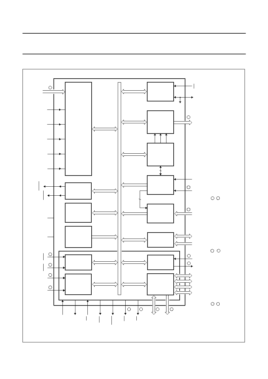
4
BLOCK DIAGRAM
handbook, full pagewidth
MBH348
3
3
1
1
4
2
0
3
3
RD
WR
AD0 to AD7
ADC0 to ADC7
A8 to A15
PSEN
XTAL2
XTAL1
EA
3
3
3
3
STADC
AV
SS
AV
DD
RST
EW
CMSR0 to CMSR5
CMT0, CMT1
RT2
T2
CT0I to CT3I
P4
P5
RXD
TXD
P3
P2
P1
P0
T0
T1
INT0
INT1
V
DD
V
SS
0
1
alternative function of port 0
alternative functions of port 1
2
3
alternative function of port 2
alternative function of port 3
4
5
alternative function of port 4
alternative function of port 5
THREE
16-BIT
COMPARA -
TORS
WITH
REGISTERS
PARALLEL
I/O PORTS
&
EXT. BUS
SERIAL
UART
PORT
8-BIT
I/O
PORTS
FOUR
16-BIT
CAPTURE
LATCHES
T2
16-BIT
TIMER/
EVENT
COUNTER
16
16
COMPARA -
TOR
OUTPUT
SELECTION
T3
WATCH -
DOG
TIMER
T0, T1
TWO 16-BIT
TIMER/
EVENT
COUNTERS
PCB
80C51
core
excluding
ROM/RAM
CPU
PROGRAM
MEMORY
DATA
MEMORY
DUAL
PWM
ADC
5
8 - bit
internal bus
8 KBYTES
ROM
PWM0
PWM1
256 BYTES
RAM
ALE
P8xC562
AV
REF
+
AV
REF
-
Fig.1 Block diagram.

1997 Apr 08
5
Philips Semiconductors
Product specification
8-bit microcontroller
P83C562; P80C562
5
FUNCTIONAL DIAGRAM
Fig.2 Functional diagram.
handbook, full pagewidth
MBH347
0
1
2
3
4
5
6
7
PORT 0
SS
V
DD
V
0
1
2
3
4
5
6
7
PORT 1
0
1
2
3
4
5
6
7
PORT 3
AD0
AD1
AD2
AD3
AD4
AD5
AD6
AD7
LOW ORDER
ADDRESS
AND
DATA BUS
alternative function
0
1
2
3
4
5
6
7
PORT 2
A8
A9
A10
A11
A12
A13
A14
A15
HIGH ORDER
ADDRESS
BUS
CT0I
CT1I
CT2I
CT3I
T2
RT2
0
1
2
3
4
5
6
7
PORT 5
0
1
2
3
4
5
6
7
PORT 4
RST
EW
alternative function
ADC0
CMSR0
ADC1
ADC2
ADC3
ADC4
ADC5
ADC6
ADC7
CMSR1
CMSR2
CMSR3
CMSR4
CMSR5
CMT0
CMT1
AVSS
AVREF
-
AVREF
+
STADC
DD
AV
PWM0
PWM1
XTAL1
XTAL2
RXD/DATA
TXD/CLOCK
T0
T1
RD
WR
INT1
INT0
P8xC562
PSEN
EA
ALE
1997 Apr 08
6
Philips Semiconductors
Product specification
8-bit microcontroller
P83C562; P80C562
6
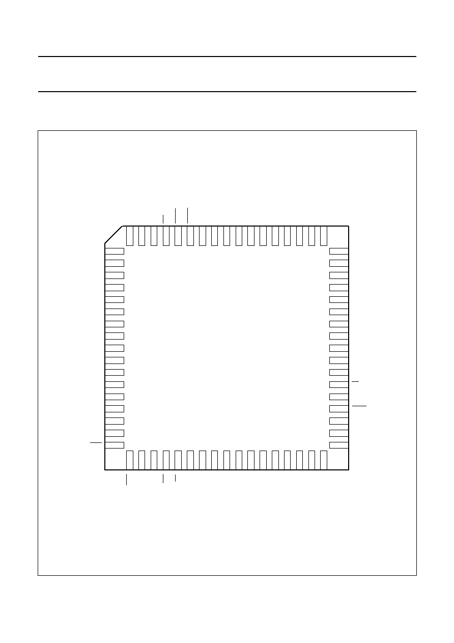
PINNING INFORMATION
6.1
Pinning
Fig.3 Pinning configuration for PLCC68 (SOT188-2) package.
handbook, full pagewidth
AVSS
P0.0/AD0
P0.1/AD1
P0.2/AD2
P0.3/AD3
P0.4/AD4
P0.5/AD5
P0.6/AD6
P0.7/AD7
ALE
P2.7/A15
P2.6/A14
P2.5/A13
AVREF
+
AVREF
-
EA
PSEN
P5.4/ADC4
P5.0/ADC0
P5.1/ADC1
P5.2/ADC2
P5.3/ADC3
P5.5/ADC5
P5.6/ADC6
P4.0/CMSR0
STADC
V
DD
EW
PWM1
PWM0
P5.7/ADC7
AV
DD
P4.2/CMSR2
P4.1/CMSR1
P4.7/CMT1
P1.0/CT0I
P1.1/CT1I
P1.2/CT2I
P3.2/INT0
P4.3/CMSR3
P4.4/CMSR4
P4.5/CMSR5
P4.6/CMT0
RST
P1.3/CT3I
P1.4/T2
P1.5/RT2
P1.6
P1.7
P3.0/RXD
P3.1/TXD
P3.6/WR
P3.5/T1
P2.2/A10
n.c.
n.c.
n.c.
XTAL 2
XTAL 1
V
SS
P2.0/A8
P2.1/A9
V
SS
P3.7/RD
P2.4/A12
P2.3/A11
P3.4/T0
P3.3/INT1
27
28
29
30
31
32
33
34
35
36
37
38
39
40
41
42
43
9
8
7
6
5
4
3
2
1
68
67
66
65
64
63
62
61
10
11
12
13
14
15
16
17
18
19
20
21
22
23
24
25
26
60
59
58
57
56
55
54
53
52
51
50
49
48
47
46
45
44
MBH349
P8xC562
1997 Apr 08
7
Philips Semiconductors
Product specification
8-bit microcontroller
P83C562; P80C562
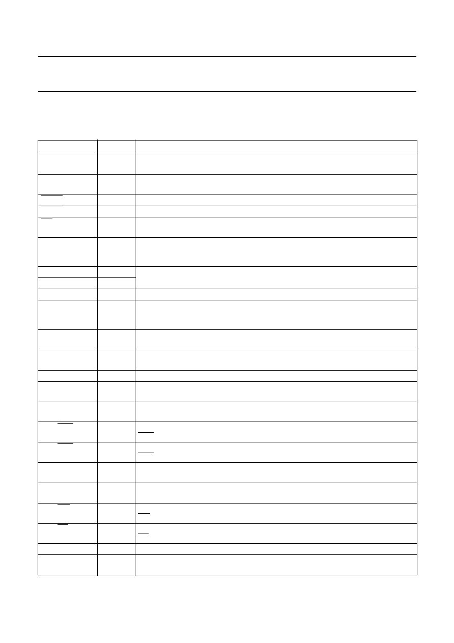
6.2
Pin description
Table 1
PLCC68 (SOT188-2)
To avoid latch-up at Power-on, the voltage at any pin at any time must lie within the range V
DD
+ 0.5 V to V
SS
-
0.5 V.
SYMBOL
PIN
DESCRIPTION
V
DD
2
Power supply, digital part (+5 V). Power supply pins during normal operation and
power reduction modes.
STADC
3
Start ADC operation: Input starting analog-to-digital conversion (ADC operation can
also be started by software). This pin must not float.
PWM0
4
Pulse Width Modulation output 0.
PWM1
5
Pulse Width Modulation output 1.
EW
6
Enable Watchdog Timer: enable for Watchdog Timer and disable Power-down mode.
This pin must not float.
P4.0/CMSR0
to
P4.5/CMSR5
7 to 12
P4.0 to P4.5: 8-bit quasi-bidirectional I/O port lines;
CMSR0 to CMSR5: Compare and Set/Reset outputs for Timer T2.
P4.6/CMT0
13
P4.6 to P4.7: 8-bit quasi-bidirectional I/O port lines;
CMT0 to CMT1: Compare and toggle outputs for Timer T2.
P4.7/CMT1
14
RST
15
Reset: Input to reset the P8x562; also generated when the Watchdog Timer overflows.
P1.0/CT0I
to
P1.3/CT3I
16 to 19
P1.0 to P1.3: 8-bit quasi-bidirectional I/O port lines;
CT0I to CT3I: Capture timer inputs for Timer 2.
P1.4/T2
20
P1.4: 8-bit quasi-bidirectional I/O port line;
T2: T2 event input (rising edge triggered).
P1.5/RT2
21
P1.5: 8-bit quasi-bidirectional I/O port line;
RT2: T2 timer reset input (rising edge triggered)
P1.6 to P1.7
22 to 23
P1.6 to P1.7: 8-bit quasi-bidirectional I/O port lines, open-drain.
P3.0/RXD
24
P3.0: 8-bit quasi-bidirectional I/O port line;
RXD: Serial input port.
P3.1/TXD
25
P3.1: 8-bit quasi-bidirectional I/O port line;
TXD: Serial output port.
P3.2/INT0
26
P3.2: 8-bit quasi-bidirectional I/O port line;
INT0: External interrupt input 0.
P3.3/INT1
27
P3.3: 8-bit quasi-bidirectional I/O port line;
INT1: External interrupt input 1.
P3.4/T0
28
P3.4: 8-bit quasi-bidirectional I/O port line;
T0: Timer 0 external input.
P3.5/T1
29
P3.5: 8-bit quasi-bidirectional I/O port line;
T1: Timer 1 external input.
P3.6/WR
30
P3.6: 8-bit quasi-bidirectional I/O port line;
WR: External Data Memory Write strobe.
P3.7/RD
31
P3.7: 8-bit quasi-bidirectional I/O port line;
RD: External Data Memory Read strobe.
n.c.
32, 33
Not connected.
XTAL2
34
Crystal Oscillator Output: output of the inverting amplifier that forms the oscillator.
Left open-circuit when an external oscillator clock is used.

1997 Apr 08
8
Philips Semiconductors
Product specification
8-bit microcontroller
P83C562; P80C562
XTAL1
35
Crystal Oscillator Input: input to the inverting amplifier that forms the oscillator, and
input to the internal clock generator. Receives the external oscillator clock signal when
an external oscillator is used.
V
SS
36, 37
Digital ground pins.
n.c.
38
Not connected.
P2.0/A08
to
P2.7/A15
39 to 46
P2.0 to P2.7: 8-bit quasi-bidirectional I/O port lines;
A08 to A15: High-order address byte for external memory.
PSEN
47
Program Store Enable: read strobe to the external program memory via Port 0 and 2.
Is activated twice each machine cycle during fetches from external program memory.
When executing out of external program memory two activations of PSEN are skipped
during each access to external data memory. PSEN is not activated (remains HIGH)
during no fetches from external program memory. PSEN can sink/source 8 LSTTL
inputs and can drive CMOS inputs without external pull-ups.
ALE
48
Address Latch Enable: latches the low byte of the address during access of external
memory in normal operation. It is activated every six oscillator periods except during an
external data memory access. ALE can sink/source 8 LSTTL inputs and can drive
CMOS inputs without an external pull-up. To prohibit the toggling of the ALE pin (RFI
noise reduction) the RFI bit in the Power Control Register must be set by software.
EA
49
External Access: if, during RESET, EA is HIGH the CPU executes out of the internal
program memory provided the program Counter is less than 8192. If, during RESET,
EA is LOW the CPU executes out of external program memory via Port 0 and Port 2.
EA is not allowed to float. EA is latched during RESET and don't care after RESET.
P0.7/AD7
to
P0.0/AD0
50 to 57
P0.7 to P0.0: 8-bit open drain bidirectional I/O port lines;
AD7 to AD0: Multiplexed Low-order address and Data bus for external memory.
AV
REF-
58
Low-end of ADC (analog-to-digital conversion) reference resistor.
AV
REF+
59
High-end of ADC (analog-to-digital conversion) reference resistor.
AV
SS
60
Ground, analog part. For ADC receiver and reference voltage.
AV
DD
61
Power supply, analog part (+5 V). For ADC receiver and reference voltage.
P5.7/ADC7
to
P5.0/ADC0
62 to 68,
1
P5.7 to P5.0: 8-bit input port lines;
ADC7 to ADC0: eight analog ADC inputs
SYMBOL
PIN
DESCRIPTION

1997 Apr 08
9
Philips Semiconductors
Product specification
8-bit microcontroller
P83C562; P80C562
7
FUNCTIONAL DESCRIPTION
The P8xC562 is a stand-alone high-performance
microcontroller designed for use in real-time applications
such as instrumentation, industrial control and specific
automotive control applications.
In addition to the 80C51 standard functions, the device
provides a number of dedicated hardware functions for
these applications.
The P8xC562 is a control-oriented CPU with on-chip
program and data memory. It can be extended with
external program memory up to 64 kbytes. It can also
access up to 64 kbytes of external data memory.
For systems requiring extra capability, the P8xC562 can
be expanded using standard memories and peripherals.
The P8xC562 has two software selectable modes of
reduced activity for further power reduction
-
Idle and
Power-down. The Idle mode freezes the CPU while
allowing the RAM, timers, serial ports and interrupt system
to continue functioning. The Power-down mode saves the
RAM contents but freezes the oscillator causing all other
chip functions to be inoperative.
8
MEMORY ORGANIZATION
The Central Processing Unit (CPU) manipulates operands
in three memory spaces; these are the 64 kbyte external
data memory, 256 byte internal data memory and the
64 kbyte internal and external program memory.
The internal data memory is divided into 3 sections: the
lower 128 bytes of RAM, the upper 128 bytes of RAM and
the 128 byte Special Function Register memory
(see Fig.4). Figure 5 shows the Special Function
Registers memory map. Internal RAM locations 0 to 127
are directly and indirectly addressable. Internal RAM
locations 128 to 155 are only indirectly addressable.
The Special Function Register locations 128 to 255 are
only directly addressable.
The internal data RAM contains four register banks (each
with eight registers), 128 addressable bits, a scratch pad
area and the stack. The stack depth is limited by the
available internal data RAM and its location is determined
by the 8-bit Stack Pointer. All registers except the Program
Counter and the four 8-register banks reside in the
Special Function Register address space. These memory
mapped registers include arithmetic registers, pointers,
I/O ports, interrupt system registers, ADC and PWM
registers, timers and serial port registers. There are
120 addressable bit locations in the SFR address space.
The P8xC562 contains 256 bytes of internal data RAM
and 52 Special Function Registers. It provides a
non-paged program memory address space to
accommodate relocatable code. Conditional branches are
performed relative to the Program Counter.
The register-indirect jump permits branching relative to a
16-bit base register with an offset provided by an 8-bit
index register. 16-bit jumps and calls permit branching to
any location in the contiguous 64 kbyte program memory
address space.
8.1
Program Memory
The program memory address space of the P83C562
consists of internal and external memory. The P83C562
has 8 kbytes of program memory on-chip. The program
memory can be externally expanded up to 64 kbytes. If the
EA pin is held HIGH, the P83C562 executes out of the
internal program memory unless the address exceeds
1FFFH then locations 2000H through to 0FFFFH are
fetched from the external program memory. If the EA pin is
held LOW, the P83C562 fetches all instructions from the
external memory. Figure 4 illustrates the program
memory address space.
By setting a mask programmable security bit (i.e. user
dependent) the ROM content is protected i.e. it cannot be
read at any time by any test mode or by any instruction in
the external program memory space. The MOVC
instructions are the only ones which have access to
program code in the internal or external program memory.
The EA input is latched during reset and is `don't care' after
reset. This implementation prevents from reading internal
program code by switching from the external program
memory to internal program memory during MOVC
instruction or an instruction that handles immediate data.
Table 2 lists the access to internal and external program
memory by the MOVC instructions when the security bit
has been set to a logic 1. If the security bit has been set to
a logic 0 there are no restrictions for the MOVC
instructions.
Table 2
Memory access by the MOVC instruction
MOVC
INSTRUCTION
PROGRAM MEMORY ACCESS
INTERNAL
EXTERNAL
MOVC in internal
program memory
YES
YES
MOVC in external
program memory
NO
YES

1997 Apr 08
10
Philips Semiconductors
Product specification
8-bit microcontroller
P83C562; P80C562
8.2
Addressing
The P8xC562 has five methods for addressing source
operands:
∑
Register
∑
Direct
∑
Register-Indirect
∑
Immediate
∑
Base-Register plus Index-Register-Indirect.
The first three methods can be used for addressing
destination operands. Most instructions have a
'destination/source' field that specifies the data type,
addressing methods and operands involved.
For operations other than MOVs, the destination operand
is also a source operand.
Access to memory addressing is as follows:
∑
Registers in one of the four 8-register banks through
Register, Direct or Register-Indirect
∑
256 bytes of internal data RAM through Direct or
Register-Indirect. Bytes 0 to 127 may be addressed
directly/indirectly. Bytes 128 to 155 share their address
locations with the SFR registers and so may only be
addressed indirectly as data RAM
∑
Special Function Registers through Direct at address
locations 128 to 255
∑
External data memory through Register-Indirect
∑
Program memory look-up tables through Base-Register
plus Index-Register-Indirect.
The P8xC562 is classified as an 8-bit device since the
internal ROM, RAM, Special Function Registers,
Arithmetic Logic Unit and external data bus are all 8-bits
wide. It performs operations on bit, nibble, byte and
double-byte data types.
Facilities are available for byte transfer, logic and integer
arithmetic operations. Data transfer, logic and conditional
branch operations can be performed directly on Boolean
variables to provide excellent bit handling.
Fig.4 Memory map.
handbook, full pagewidth
MBC745
INDIRECT ONLY
DIRECT AND
INDIRECT
255
127
0
EXTERNAL
(EA = 0)
INTERNAL
(EA = 1)
INTERNAL DATA MEMORY
EXTERNAL
DATA MEMORY
PROGRAM MEMORY
EXTERNAL
64K
64K
8192
8191
0
OVERLAPPED SPACE
0
8191
0
SPECIAL
FUNCTION
REGISTERS

1997 Apr 08
11
Philips Semiconductors
Product specification
8-bit microcontroller
P83C562; P80C562
Fig.5 Special Function Register memory map.
handbook, full pagewidth
MBH346
FE
FF
FD
FC
FB
FA
F9
F8
F6
F7
F5
F4
F3
F2
F1
F0
EE
EF
ED
EC
EB
EA
E9
E8
E6
E7
E5
E4
E3
E2
E1
E0
D6
D7
D5
D4
D3
D2
D1
D0
CE
CF
CD CC
CB
CA C9
C8
C6
C7
C5
C4
C3
C2
C1
C0
BIT ADDRESS
REGISTER
MNEMONIC
FFH
DIRECT
BYTE
ADDRESS (HEX)
FEH
FDH
FCH
F8H
F0H
EFH
EEH
EDH
ECH
EBH
EAH
E8H
E0H
DBH
DAH
D9H
D8H
D0H
CFH
CEH
CDH
CCH
CBH
CAH
C9H
C8H
C6H
C5H
C4H
C0H
SFRs containing
directly addressable
bits
Reserved for I
2
C-bus
T3
PWMP
PWM1
PWM0
IP1
B
RTE
STE
# TMH2
# TML2
CTCON
TM2CON
IEN1
ACC
PSW
# CTH3
# CTH2
# CTH1
# CTH0
CMH2
CMH1
CMH0
TM2IR
# ADCH
ADCON
# P5
P4
# denotes read-only registers

1997 Apr 08
12
Philips Semiconductors
Product specification
8-bit microcontroller
P83C562; P80C562
handbook, full pagewidth
MGA151
BE
BF
BD
BC
BB
BA
B9
B8
B6
B7
B5
B4
B3
B2
B1
B0
AE
AF
AD
AC
AB
AA
A9
A8
A6
A7
A5
A4
A3
A2
A1
A0
9E
9F
9D
9C
9B
9A
99
98
96
97
95
94
93
92
91
90
8E
8F
8D
8C
8B
8A
89
88
86
87
85
84
83
82
81
80
BIT ADDRESS
REGISTER
MNEMONIC
DIRECT
BYTE
ADDRESS (HEX)
B8H
B0H
AFH
AEH
ADH
ACH
ABH
AAH
A8H
A0H
99H
98H
90H
8DH
8CH
8BH
8AH
89H
88H
87H
83H
82H
81H
80H
SFRs containing
directly addressable
bits
IP0
P3
# CTL3
P2
S0BUF
S0CON
P1
TH1
TH0
TL1
TL0
TMOD
PCON
DPH
DPL
SP
P0
# denotes read-only registers
# CTL2
# CTL1
# CTL0
CML2
CML1
CML0
IEN0
TCON
A9H
Fig.6 Special Function Register memory map (continued).

1997 Apr 08
13
Philips Semiconductors
Product specification
8-bit microcontroller
P83C562; P80C562
9
I/O FACILITIES
The P8xC562 has six 8-bit ports. Ports 0 to 3 are the same
as in the 80C51, with the exception of the additional
functions of Port 1. The parallel I/O function of Port 4 is
equal to that of Ports 1, 2 and 3. Port 5 has a parallel input
port function, but has no function as an output port.
Ports 0 to 5 perform the following alternative functions:
Port 0 Provides the multiplexed low-order address and
data bus used for expanding the P8xC562 with
standard memories and peripherals.
Port 1 is used for a number of special functions:
∑
4 capture inputs (or external interrupt request inputs if
capture information is not utilized)
∑
External counter input
∑
External counter reset input.
Port 2 Provides the high-order address bus when
expanding the P8xC562 with external program
memory and/or external data memory.
Port 3 Pins can be configured individually to provide:
∑
External interrupt request inputs
∑
Counter inputs
∑
Serial port receiver input and transmitter output
∑
Control signals to READ and WRITE external data
memory.
Port 4 Can be configured to provide signals indicating a
match between timer counter T2 and its compare
registers.
Port 5 May be used in conjunction with the ADC interface.
Unused analog inputs can be used as digital inputs.
As Port 5 lines may be used as inputs to the ADC,
these digital inputs have an inherent hysteresis to
prevent the input logic from drawing too much
current from the power lines when driven by analog
signals. Channel-to-channel crosstalk should be
taken into consideration when both digital and
analog signals are simultaneously input to Port 5
(see Chapter 20).
All ports are bidirectional with the exception of Port 5 which
is an input port. Alternative function bits which are not used
may be used as normal bidirectional I/O pins.
The generation or use of a Port 1, Port 3 or Port 4 pin as
an alternative function is carried out automatically by the
P8xC562 provided the associated Special Function
Register bit is set HIGH.
In addition to the standard 8-bit ports, the I/O facilities of
the P8xC562 also include a number of special I/O lines.
Fig.7 I/O buffers in the P8xC562 (Ports 2, 3, 4 and P1.0 to P1.5).
handbook, full pagewidth
MLA513
p1
p2
p3
input data
read port pin
2 oscillator
periods
n
strong pull-up
I/O PIN
PORT
+5 V
I1
Q
from port latch
INPUT
BUFFER

1997 Apr 08
14
Philips Semiconductors
Product specification
8-bit microcontroller
P83C562; P80C562
10 PULSE WIDTH MODULATED OUTPUTS
Two pulse width modulated output channels are provided
with the P8xC562. These channels output pulses of
programmable length and interval. The repetition
frequency is defined by an 8-bit prescaler PWMP which
generates the clock for the counter. Both the prescaler and
counter are common to both PWM channels. The 8-bit
counter counts modulo 255 i.e. from 0 to 254 inclusive.
The value of the 8-bit counter is compared to the contents
of two registers: PWM0 and PWM1.
Provided the contents of either of these registers is greater
than the counter value, the output of PWM0 or PWM1 is
set LOW. If the contents of these registers are equal to, or
less than the counter value, the output will be HIGH.
The pulse width ratio is therefore defined by the contents
of the registers PWM0 and PWM1.
The pulse width ratio is in the range of 0 to 255/255 and
may be programmed in increments of 1/255.
The repetition frequency f
PWM
, at the PWMn outputs is
given by:
When using an oscillator frequency of 16 MHz for
example, the above formula would give a repetition
frequency range of 123 Hz to 31.4 kHz.
By loading the PWM registers with either 00H or FFH, the
PWM outputs can be retained at a constant HIGH or LOW
level respectively. When loading FFH to the PWM
registers, the 8-bit counter will never actually reach this
value. Both PWMn output pins are driven by push-pull
drivers, and are not shared with any other function.
f
PWM
f
OSC
2
1
PWMP
+
(
)
◊
255
◊
-------------------------------------------------------------
=
Fig.8 Functional diagram of Pulse Width Modulated outputs.
handbook, full pagewidth
MBC746
I
N
T
E
R
N
A
L
B
U
S
f osc
PWMP
PWM1
PRESCALER
8-BIT COUNTER
1/2
PMW0
8-BIT COMPARATOR
8-BIT
COMPARATOR
OUTPUT
BUFFER
PWM1
OUTPUT
BUFFER
PWM0

1997 Apr 08
15
Philips Semiconductors
Product specification
8-bit microcontroller
P83C562; P80C562
10.1
Prescaler Frequency Control Register (PWMP)
Table 3
Prescaler Frequency Control Register (SFR address FEH)
Table 4
Description of PWMP bits
10.2
Pulse Width Register 0 (PWM0)
Table 5
Pulse Width Register 0 (SFR address FCH)
Table 6
Description of PWM0 bits
10.3
Pulse Width Register 1 (PWM1)
Table 7
Pulse Width Register 1 (SFR address FDH)
Table 8
Description of PWM1 bits
7
6
5
4
3
2
1
0
PWMP.7
PWMP.6
PWMP.5
PWMP.4
PWMP.3
PWMP.2
PWMP.1
PWMP.0
BIT
SYMBOL
DESCRIPTION
7
to
0
PWMP.7
to
PWMP.0
Prescaler division factor.
The prescaler division factor = (PWMP) + 1.
7
6
5
4
3
2
1
0
PWM0.7
PWM0.6
PWM0.5
PWM0.4
PWM0.3
PWM0.2
PWM0.1
PWM0.0
BIT
SYMBOL
DESCRIPTION
7
to
0
PWM0.7
to
PWM0.0
Pulse width ratio.
7
6
5
4
3
2
1
0
PWM1.7
PWM1.6
PWM1.5
PWM1.4
PWM1.3
PWM1.2
PWM1.1
PWM1.0
BIT
SYMBOL
DESCRIPTION
7
to
0
PWM1.7
to
PWM1.0
Pulse width ratio.
LOW/HIGH ratio of PWMn signals
PWMn
(
)
255
PWMn
(
)
≠
------------------------------------------
=
LOW/HIGH ratio of PWMn signals
PWMn
(
)
255
PWMn
(
)
≠
------------------------------------------
=

1997 Apr 08
16
Philips Semiconductors
Product specification
8-bit microcontroller
P83C562; P80C562
11 ANALOG-TO-DIGITAL CONVERTER (ADC)
The completion of the 8-bit ADC conversion is flagged by
ADCI in the ADCON register and the result is stored in
Special Function Register ADCH.
An ADC conversion in progress is unaffected by an
external or software ADC start. The result of a completed
conversion remains unaffected provided ADCI = 1. While
ADCS = 1 or ADCI = 1, a new ADC start will be blocked
and consequently lost.
An ADC conversion already in progress is aborted when
the Idle or Power-down mode is entered. The result of a
completed conversion (ADCI = 1) remains unaffected
when entering the Idle mode.
If ADCI is cleared by software and ADCS is set at the same
time, a new analog-to-digital conversion with the same
channel number, may be started. However, it is
recommended to reset ADCI before ADCS is set.
11.1
Analog input pins
The analog input circuitry consists of an 8-input analog
multiplexer and an ADC with 8-bit resolution. The analog
reference voltage and analog power supplies are
connected via separate input pins. The conversion takes
24 machine cycles i.e. 18
µ
s at an oscillator frequency of
16 MHz.
The ADC is controlled using the ADC Control Register
(ADCON). Input channels are selected by the analog
multiplexer, using bits AADR.0 to AADR.2 in ADCON.
Fig.9 Functional diagram of analog input.
handbook, full pagewidth
MBH350
ADC0
ANALOG INPUT
MULTIPLEXER
8-BIT ADC
ADCON
1
2
3
4
5
6
7
0
1
2
3
4
5
6
7
0
STADC
analog reference
supply (analog part)
ground (analog part)
ADCH
INTERNAL BUS
ADC1
ADC2
ADC3
ADC4
ADC5
ADC6
ADC7
1997 Apr 08
17
Philips Semiconductors
Product specification
8-bit microcontroller
P83C562; P80C562
11.2
ADC Control Register (ADCON)
Table 9
ADC Control Register (SFR address C5H)
Table 10 Description of ADCON bits
Table 11 Function of ADCI and ADCS bits
7
6
5
4
3
2
1
0
-
-
ADEX
ADCI
ADCS
AADR2
AADR1
AADR0
BIT
SYMBOL
DESCRIPTION
7
-
These two bits are reserved.
6
-
5
ADEX
Enable external start: start of conversion by STADC. If ADEX = 0, then conversion
can not be started externally by STADC (only by software by setting ADCS).
If ADEX = 1, then conversion can be started externally by a rising edge on STADC or by
software.
4
ADCI
ADC interrupt flag: this flag is set when an analog-to-digital conversion result is ready
to be read. An interrupt is invoked if it is enabled. The flag must be cleared by the
interrupt service routine. While this flag is set, the ADC cannot start a new conversion.
ADCI cannot be set by software.
3
ADCS
ADC start and status: setting this bit starts an ADC conversion. It may be set by
software or by the external signal STADC. The ADC logic ensures that this signal is
HIGH while the ADC is busy. On completion of the conversion, ADCS is reset
immediately after the interrupt flag has been set. ADCS can not be reset by software nor
can a new conversion be started if either ADCS or ADCI is HIGH.
2
AADR.2
Analog input select: these three bits are used to select one of the eight analog inputs
of Port 5, for conversion. A selection can only be made when ADCI and ADCS are both
LOW. AADR2 is the most significant bit (e.g. 100 selects the ADC4 analog input
channel).
1
AADR.1
0
AADR.0
ADCI
ADCS
OPERATION
0
0
ADC not busy, a conversion can be started.
0
1
ADC busy, start of a new conversion is blocked.
1
0
Conversion completed; start of a new conversion is blocked.
1
1
Intermediate status for a maximum of one machine cycle before conversion is
completed.

1997 Apr 08
18
Philips Semiconductors
Product specification
8-bit microcontroller
P83C562; P80C562
12 TIMER/ COUNTERS
The P8xC562 contains:
∑
Three 16-bit timer/event counters: Timer 0, Timer 1 and
Timer 2
∑
One 8-bit Watchdog Timer.
12.1
Timer 0 and Timer 1
Timer 0 and Timer 1 may be programmed to carry out the
following operations:
∑
Measure time intervals and pulse durations
∑
Count events
∑
Generate interrupt requests.
Timer 0 and Timer 1 can also be programmed
independently to operate in three modes:
Mode 0 8-bit timer or 8-bit counter each with
divide-by-32 prescaler
Mode 1 16-bit time-interval or event counter
Mode 2 8-bit time-interval or event counter with automatic
reload upon overflow.
Timer 0 can be programmed to operate in an additional
mode as follows:
Mode 3 one 8-bit time-interval or event counter and one
8-bit time-interval counter.
When Timer 0 is in Mode 3, Timer 1 can be programmed
to operate in Modes 0, 1 or 2 but cannot set an interrupt
request flag or generate an interrupt. However, the
overflow from Timer 1 can be used to pulse the serial port
transmission-rate generator.
The frequency handling range of these counters with a
16 MHz crystal is as follows:
∑
In the timer function, the timer is incremented at a
frequency of 1.33 MHz; a division by 12 of the oscillator
frequency
∑
0 Hz to an upper limit of 0.66 MHz when programmed
for external inputs.
Both internal and external inputs can be gated to the
counter by a second external source for directly measuring
pulse durations.
The counters are started and stopped under software
control. Each one sets its interrupt request flag when it
overflows from all logic 1s to all logic 0s (or automatic
reload value), with the exception of Mode 3 as previously
described.
12.2
Timer T2 Capture and Compare Logic
Timer T2 is a 16-bit timer/counter which has, coupled to it,
capture and compare facilities. The operational diagram is
shown in Fig.10.
The 16-bit timer/counter is clocked via a prescaler with a
programmable division factor of 1, 2, 4 or 8. The input of
the prescaler is clocked with
1
/
12
of the oscillator
frequency, or with positive edges on the T2 input, or it is
switched to the off position. The prescaler is cleared if its
division factor or its input source is changed, or if the
timer/counter is reset. T2 is readable on-the-fly, but
possesses no extra read latches; this means that software
precautions have to be taken against misinterpretation on
overflow from least to most significant byte during a read.
T2 is not loadable and is reset by the RST signal or at the
positive edge of the input signal RT2, if enabled. In the Idle
mode the timer/counter and prescaler are reset and
halted.
T2 is connected to four 16-bit Capture Registers: CT0,
CT1, CT2 and CT3. These registers are loaded with the
contents of T2 and an interrupt is requested upon receipt
of the input signals CT0I, CT1I, CT2I or CT3I. These input
signals are shared with Port 1. Using the Capture Register
(CTCON), these inputs may invoke capture and interrupt
request on a positive or negative edge or on both edges.
If neither a positive nor a negative edge is selected for a
capture input, no capture or interrupt request can be
generated by this input.
The contents of the Compare Registers CM0, CM1 and
CM2 are continually compared with the counter value of
Timer 2. When a match is found an interrupt may be
invoked. Using the match signal of CM0, the controller sets
bits 0 to 5 of Port 4, if the corresponding bits of the Set
Enable Register are logic 1s.
Considering a match with CM1, if the corresponding bits of
the Reset/toggle Enable Register (RTE) are logic 1, then
the controller will use the match signal to reset bits 0 to 5
of Port 4. Bits 6 and 7 of Port 4 may be toggled by the
signal that indicates a match of Timer T2 and CM2 if the
corresponding bits of RTE are logic 1. CM0, CM1 and CM2
are reset by the RST signal.
Port 4 can be read and written by software without
affecting the toggle, set and reset signals. At byte overflow
of the least significant byte, or at a 16-bit overflow of the
timer/counter, an interrupt sharing the same interrupt
vector is requested. Either one or both of these overflows
can be programmed to request an interrupt.
All interrupt flags must be reset by software.

1997 Apr 08
19
Philips Semiconductors
Product specification
8-bit microcontroller
P83C562; P80C562
Fig.10 Block diagram of Timer T2 configuration.
handbook, full pagewidth
MBC755
STE
RTE
I/O port 4
= set
= reset
= toggle
= toggle status
S
R
T
TG
T2 SFR address: TML2 = lower 8 bits
TMH2 = higher 8 bits
INT
COMP
CM0 (S)
INT
COMP
CM1 (R)
INT
COMP
CM2 (T)
CT3I
INT
CTI3
CT3
off
f osc
T2
RT2
T2ER
external reset
enable
PRESCALER
1/12
T2 COUNTER
8-bit overflow interrupt
16-bit overflow interrupt
CT2I
INT
CTI2
CT2
CT1I
INT
CTI1
CT1
CT0I
INT
CTI0
CT0
P4.0
P4.1
P4.2
P4.3
P4.4
P4.5
P4.6
P4.7
R
R
R
R
R
R
T
T
S
S
S
S
S
S
TG
TG
1997 Apr 08
20
Philips Semiconductors
Product specification
8-bit microcontroller
P83C562; P80C562
12.2.1
T2 C
ONTROL
R
EGISTER
(TM2CON)
Table 12 T2 Control Register (SFR address EAH)
Table 13 Description of TM2CON bits
Table 14 Timer 2 prescaler select
Table 15 Timer 2 mode select
7
6
5
4
3
2
1
0
T2IS1
T2IS0
T2ER
T2B0
T2P1
T2P0
T2MS1
T2MS0
BIT
SYMBOL
DESCRIPTION
7
T2IS1
Timer 2 16-bit overflow interrupt select.
6
T2IS0
Timer 2 byte overflow interrupt select.
5
T2ER
Timer 2 external reset enable.
4
T2B0
Timer 2 byte overflow interrupt flag.
3
T2P1
Timer 2 prescaler select (see Table 14).
2
T2P0
1
T2MS1
Timer 2 mode select (see Table 15).
0
T2MS0
T2P1
T2P0
T2 CLOCK
0
0
Clock source
0
1
1
/
2
clock source
1
0
1
/
4
clock source
1
1
1
/
8
clock source
T2MS1
T2MS0
MODE
0
0
Timer T2 is halted
0
1
T2 clock source =
1
/
12
◊
f
OSC
1
0
Test mode; do not use
1
1
T2 clock source = pin T2
1997 Apr 08
21
Philips Semiconductors
Product specification
8-bit microcontroller
P83C562; P80C562
12.2.2
C
APTURE
C
ONTROL
R
EGISTER
(CTCON)
Table 16 Capture Control Register (SFR address EBH)
Table 17 Description of CTCON bits
12.2.3
I
NTERRUPT
F
LAG
R
EGISTER
(TM2IR)
Table 18 Interrupt Flag Register (SFR address C8H)
Table 19 Description of TM2IR bits (see notes 1 and 2)
Notes
1. Interrupt Enable Register 1 (IEN1) is used to enable/disable Timer 2 interrupts.
2. Interrupt Priority Register 1 (IP1) is used to determine the Timer 2 interrupt priority.
7
6
5
4
3
2
1
0
CTN3
CTP3
CTN2
CTP2
CTN1
CTP1
CTN0
CTP0
BIT
SYMBOL
DESCRIPTION
7
CTN3
Interrupt triggered on negative edge of CT3I.
6
CTP3
Interrupt triggered on positive edge of CT3I.
5
CTN2
Interrupt triggered on negative edge of CT2I.
4
CTP2
Interrupt triggered on positive edge of CT2I
3
CTN1
Interrupt triggered on negative edge of CT1I.
2
CTP1
Interrupt triggered on positive edge of CT1I.
1
CTN0
Interrupt triggered on negative edge of CT0I.
0
CTP0
Interrupt triggered on positive edge of CT0I.
7
6
5
4
3
2
1
0
T2OV
CMI2
CMI1
CMI0
CTI3
CTI2
CTI1
CTI0
BIT
SYMBOL
DESCRIPTION
7
T2OV
T2: 16-bit overflow interrupt flag.
6
CMI2
CM2: interrupt flag.
5
CMI1
CM1: interrupt flag.
4
CMI0
CM0: interrupt flag.
3
CTI3
CT3: interrupt flag.
2
CTI2
CT2: interrupt flag.
1
CTI1
CT1: interrupt flag.
0
CTI0
CT0: interrupt flag.
1997 Apr 08
22
Philips Semiconductors
Product specification
8-bit microcontroller
P83C562; P80C562
12.2.4
S
ET
E
NABLE
R
EGISTER
(STE)
Table 20 Set Enable Register (SFR address EEH)
Table 21 Description of STE bits (see notes 1 and 2)
Notes
1. If STE.n is LOW then P4.n is not affected by a match of CM0 and T2 (n = 0 to 5).
2. STE.6 and STE.7 are read only.
12.2.5
R
ESET
/T
OGGLE
E
NABLE REGISTER
(RTE)
Table 22 Reset/toggle enable register (SFR address EFH)
Table 23 Description of RTE bits (note 1)
Note
1. If RTE.n is LOW then P4.n is not affected by a match of CM1 and T2 or CM2 and T2. For more information, refer to
the 8051-based
"8-bit Microcontrollers Data Handbook IC20".
7
6
5
4
3
2
1
0
TG47
TG46
SP45
SP44
SP43
SP42
SP41
SP40
BIT
SYMBOL
DESCRIPTION
7
TG47
If HIGH then P4.7 is reset on the next toggle, if LOW P4.7 is set on the next toggle.
6
TG46
If HIGH then P4.6 is reset on the next toggle, if LOW P4.6 is set on the next toggle.
5
SP45
If HIGH the P4.5 is set on a match of CM0 and T2.
4
SP44
If HIGH the P4.4 is set on a match of CM0 and T2.
3
SP43
If HIGH the P4.3 is set on a match of CM0 and T2.
2
SP42
If HIGH the P4.2 is set on a match of CM0 and T2.
1
SP41
If HIGH the P4.1 is set on a match of CM0 and T2.
0
SP40
If HIGH the P4.0 is set on a match of CM0 and T2.
7
6
5
4
3
2
1
0
TP47
TP46
RP45
RP44
RP43
RP42
RP41
RP40
BIT
SYMBOL
DESCRIPTION
7
TP47
If HIGH then P4.7 toggles on a match of CM2 and T2.
6
TP46
If HIGH then P4.6 toggles on a match of CM2 and T2.
5
RP45
If HIGH then P4.5 is reset on a match of CM1 and T2.
4
RP44
If HIGH then P4.4 is reset on a match of CM1 and T2.
3
RP43
If HIGH then P4.3 is reset on a match of CM1 and T2.
2
RP42
If HIGH then P4.2 is reset on a match of CM1 and T2.
1
RP41
If HIGH then P4.1 is reset on a match of CM1 and T2.
0
RP40
If HIGH then P4.0 is reset on a match of CM1 and T2.

1997 Apr 08
23
Philips Semiconductors
Product specification
8-bit microcontroller
P83C562; P80C562
12.3
Watchdog Timer (T3)
In addition to Timer T2 and the standard timers, a
Watchdog Timer is also available, consisting of an 11-bit
prescaler and a 8-bit timer. The functional diagram of the
Watchdog Timer is shown in Fig.11. The timer is
incremented every t seconds,
where:
When a timer overflow occurs, the microcontroller is reset
and a reset output pulse is generated at the RST pin.
To prevent a system reset the timer must be reloaded in
time by the application software. If the processor suffers a
hardware/ software malfunction, the software will fail to
reload the timer. This failure will produce a reset upon
overflow thus preventing the processor running out of
control.
t
12
2048
◊
f
OSC
--------------------------
=
The Watchdog Timer can only be reloaded if the condition
flag WLE in the Power Control Register has been
previously set by software. At the moment the counter is
loaded the condition flag is automatically cleared.
The timer interval between the timer's reloading and
occurrence of a reset, is dependent upon the reloaded
value. For example, this may range from 2 ms to 0.5 s
when using an oscillator frequency of 12 MHz. In the Idle
state the Watchdog Timer and reset circuitry remain
active.
The Watchdog Timer is controlled by the Enable
Watchdog pin (EW). A logic 0 enables the Watchdog
Timer and disables the Power-down mode. A logic 1
disables the Watchdog Timer and enables the
Power-down mode.
Fig.11 Functional diagram of Watchdog Timer.
handbook, full pagewidth
MBC753
INTERNAL BUS
write
T3
PRESCALER
11-BIT
TIMER T3 (8-BIT)
LOAD
CLEAR
overflow
internal
reset
LOADEN
EW
LOADEN
PCON.4
PCON.1
CLEAR
WLE
PD
R
RST
RST
P
VDD
INTERNAL BUS
f
/12
osc

1997 Apr 08
24
Philips Semiconductors
Product specification
8-bit microcontroller
P83C562; P80C562
13 SERIAL I/O
The P8xC562 is equipped with a full duplex UART port and
is identical to the serial port of the 80C51 (see
`Single-chip
8-bit Microcontrollers User Manual' .
14 INTERRUPT SYSTEM
External events and the real-time driven on-chip
peripherals require service by the CPU asynchronously to
the execution of any particular section of code. To tie the
asynchronous activities of these functions to normal
program execution a multiple-source, two-priority-level,
nested interrupt system is provided. The interrupt system
is shown in Fig.12. Interrupt response latency is from
2.25
µ
s to 6
µ
s when using a 16 MHz crystal.
The P8xC562 acknowledges interrupt requests from
14 sources as follows:
∑
INT0 and INT1: externally via pins P3.2/INT0 and
P3.3/INT1 respectively
∑
Timer 0 and Timer 1: from the two internal counters
∑
Timer T2 (8 separate interrupts): 4 capture interrupts,
3 compare interrupts and an overflow interrupt. If the
Capture Register remains unused and its contents are
'don't care', then the corresponding input pin CTnI may
be used as a positive and/or negative edge triggered
external interrupt.
∑
ADC conversion completed interrupt
∑
UART serial I/O port interrupt.
Each interrupt vectors to a separate location in program
memory for its service routine. Each source can be
individually enabled or disabled by a corresponding bit in
the IEN0 or IEN1 registers, in addition each interrupt may
be programmed to a high or low priority level using the
corresponding bit in the IP0 or IP1 registers. All enabled
sources can be globally disabled or enabled. Both external
interrupts can be programmed to be level-activated or
transition-activated; an active LOW level allows
'wire-ORing' of several interrupt sources to the input pin.
14.1
Interrupt Vectors
Table 24 gives the vector address in Program Memory
where the appropriate interrupt service routine is located.
Table 24 Interrupt vectors
14.2
Interrupt priority
Each interrupt source can be either high priority or low
priority. If both priorities are requested simultaneously, the
processor will branch to the high priority vector. If there are
simultaneous requests from sources of the same priority,
then interrupts will be serviced in the following order:
X0, ADC, T0, CT0, CM0, X1, CT1, CM1, T1, CT2, CM2,
S0, CT3, T2.
A low priority interrupt routine can only be interrupted by a
high priority interrupt. A high priority interrupt routine can
not be interrupted.
SOURCE
SYMBOL
VECTOR
External 0
X0
0003H
Timer 0 overflow
T0
000BH
External 1
X1
0013H
Timer 1 overflow
T1
001BH
Serial I/O 0 (UART)
S0
0023H
T2 capture 0
CT0
0033H
T2 capture 1
CT1
003BH
T2 capture 2
CT2
0043H
T2 capture 3
CT3
004BH
ADC completion
ADC
0053H
T2 compare 0
CM0
005BH
T2 compare 1
CM1
0063H
T2 compare 2
CM2
006BH
T2 overflow
T2
0073H

1997 Apr 08
25
Philips Semiconductors
Product specification
8-bit microcontroller
P83C562; P80C562
Fig.12 Interrupt system.
handbook, full pagewidth
interrupt
sources
source enable
global enable
interrupt enable registers
a1
a2
b1
b2
c1
c2
d1
d2
e1
e2
f1
f2
g1
g2
h1
h2
i1
i2
j1
j2
k1
k2
l1
l2
m1
m2
n1
n2
interrupt priority
registers
a1
SOURCE
IDENTIFICATION
vector
b1
c1
d1
e1
f1
g1
h1
i1
j1
k1
l1
m1
n1
o1
high
priority
interrupt
request
MBH345
a2
SOURCE
IDENTIFICATION
vector
b2
c2
d2
e2
f2
g2
h2
i2
j2
k2
l2
m2
n2
o2
low
priority
interrupt
request
polling hardware
CT3I
CT2I
CT1I
CT0I
INT0
INT1
EXTERNAL
INTERRUPT
REQUEST 0
ADC
TIMER 0
OVERFLOW
TIMER 2
CAPTURE 0
TIMER 2
COMPARE 0
EXTERNAL
INTERRUPT
REQUEST 1
TIMER 2
CAPTURE 1
TIMER 2
COMPARE 1
TIMER 1
OVERFLOW
TIMER 2
CAPTURE 2
TIMER 2
COMPARE 2
UART
SERIAL
PORT
TIMER 2
CAPTURE 3
TIMER T2
OVERFLOW
T
R
1997 Apr 08
26
Philips Semiconductors
Product specification
8-bit microcontroller
P83C562; P80C562
14.3
Interrupt Enable and Priority Registers
14.3.1
I
NTERRUPT
E
NABLE
R
EGISTER
0 (IEN0)
Table 25 Interrupt Enable Register 0 (SFR address A8H)
Table 26 Description of IEN0 bits (note 1)
Note
1. Logic 0 = interrupt disabled; Logic 1 = interrupt enabled.
14.3.2
I
NTERRUPT
E
NABLE REGISTER
1 (IEN1)
Table 27 Interrupt Enable Register 1 (SFR address E8H)
Table 28 Description of IEN1 bits (note 1)
Note
1. Logic 0 = interrupt disabled; Logic 1 = interrupt enabled.
7
6
5
4
3
2
1
0
EA
EAD
-
ES0
ET1
EX1
ET0
EX0
BIT
SYMBOL
DESCRIPTION
7
EA
General enable/disable control. If EA = 0, then no interrupt is enabled. If EA =1, then
any individually enabled interrupt will be accepted.
6
EAD
Enable ADC interrupt.
5
-
Reserved.
4
ES0
Enable SIO (UART) interrupt.
3
ET1
Enable Timer 1 interrupt.
2
EX1
Enable External interrupt.
1
ET0
Enable Timer 0 interrupt.
0
EX0
Enable External 0 interrupt.
7
6
5
4
3
2
1
0
ET2
ECM2
ECM1
ECM0
ECT3
ECT2
ECT1
ECT0
BIT
SYMBOL
DESCRIPTION
7
ET2
Enable T2 overflow interrupt(s).
6
ECM2
Enable T2 comparator 2 interrupt.
5
ECM1
Enable T2 comparator 1 interrupt.
4
ECM0
Enable T2 comparator 0 interrupt.
3
ECT3
Enable T2 capture register 3 interrupt.
2
ECT1
Enable T2 capture register 2 interrupt.
1
ECT1
Enable T2 capture register 1 interrupt.
0
ECT0
Enable T2 capture register 0 interrupt.
1997 Apr 08
27
Philips Semiconductors
Product specification
8-bit microcontroller
P83C562; P80C562
14.3.3
I
NTERRUPT PRIORITY REGISTER
0 (IP0)
Table 29 Interrupt Priority Register 0 (SFR address B8H)
Table 30 Description of IP0 bits (note 1)
Note
1. A logic 0 = low priority; a logic 1 = high priority.
14.3.4
I
NTERRUPT
P
RIORITY
R
EGISTER
1 (IP1)
Table 31 Interrupt Priority Register 1 (SFR address F8H)
Table 32 Description of IP1 bits (note 1)
Note
1. A logic 0 = low priority; a logic 1 = high priority.
7
6
5
4
3
2
1
0
-
PAD
-
PS0
PT1
PX1
PT0
PX0
BIT
SYMBOL
DESCRIPTION
7
-
Reserved.
6
PAD
ADC interrupt priority level.
5
-
Reserved.
4
PS0
SIO0 (UART) interrupt priority level.
3
PT1
Timer 1 interrupt priority level.
2
PX1
External interrupt 1 priority level.
1
PT0
Timer 0 interrupt priority level.
0
PX0
External interrupt 0 priority level.
7
6
5
4
3
2
1
0
PT2
PCM2
PCM1
PCM0
PCT3
PCT2
PCT1
PCT0
BIT
SYMBOL
DESCRIPTION
7
PT2
T2 overflow interrupt(s) priority level.
6
PCM2
T2 comparator 2 interrupt priority interrupt level.
5
PCM1
T2 comparator 1 interrupt priority interrupt level.
4
PCM0
T2 comparator 0 interrupt priority interrupt level.
3
PCT3
T2 capture register 3 priority interrupt level.
2
PCT2
T2 capture register 2 priority interrupt level.
1
PCT1
T2 capture register 1 priority interrupt level.
0
PCT0
T2 capture register 0 priority interrupt level.

1997 Apr 08
28
Philips Semiconductors
Product specification
8-bit microcontroller
P83C562; P80C562
15 REDUCED POWER MODES
15.1
Idle and Power-down operation
Idle mode operation permits the interrupt, serial ports and
timer blocks to continue to function while the CPU is
halted. The Idle and Power-down clock configuration is
shown in Fig.13. The following functions are switched off
when the processor enters the Idle mode.
∑
Timer T2 - stopped and reset
∑
PWM0 and PWM1 - reset, output HIGH
∑
ADC - aborted if in progress.
The following functions remain active during Idle mode.
These functions may generate an interrupt or reset and
thus end the Idle mode.
∑
Timer 0, Timer 1
∑
Timer T3
∑
SIO
∑
External Interrupt.
The Power-down operation freezes the oscillator.
The Power-down mode can only be activated by setting
the PD bit in the PCON register. The PD bit can only be set
if the EW input is HIGH.
15.1.1
I
DLE MODE
The instruction that sets PCON.0 is the last instruction
executed in the normal operating mode before Idle mode
is activated. Once in the Idle mode, the CPU status is
preserved in its entirety: the Stack Pointer, Program
Counter, Program Status Word, Accumulator, RAM and all
other registers maintain their data during Idle mode.
The status of the external pins during Idle mode is shown
in Table 33.
There are two ways to terminate the Idle mode:
∑
Activation of any enabled interrupt will cause PCON.0 to
be cleared by hardware terminating the Idle mode.
The interrupt is serviced, and following the return from
interrupt instruction RETI, the next instruction to be
executed will be the one which follows the instruction
that wrote a logic 1 to PCON.0. The flag bits GF0 and
GF1 may be used to determine whether the interrupt
was received during normal execution or during the Idle
mode. For example, the instruction that writes to
PCON.0 can also set or clear one or both flag bits. When
Idle mode is terminated by an interrupt, the service
routine can examine the status of the flag bits.
∑
The second way of terminating the Idle mode is with an
external hardware reset, or an internal reset caused by
an overflow of the Watchdog Timer (T3). Since the
oscillator is still running, the hardware reset is required
to be active for two machine cycles (24 oscillator periods
but at least 2
µ
s) to complete the reset operation.
15.1.2
P
OWER
-
DOWN MODE
The instruction that sets PCON.1 is the last executed prior
to going into the Power-down mode. Once in Power-down
mode, the oscillator is stopped. Only the contents of the
on-chip RAM are preserved. The Special Function
Registers are not saved. A hardware reset is the only way
of exiting the Power-down mode.
In the Power-down mode, V
DD
may be reduced to
minimize circuit power consumption. The supply voltage
must not be reduced until the Power-down mode is
entered, and must be restored before the hardware reset
is applied which will free the oscillator. Reset should not be
released until the oscillator has restarted and stabilized.
The status of the external pins during Power-down mode
is shown in Table 33. If the Power-down mode is activated
while in external program memory, the port data that is
held in the Special Function Register P2 is restored to
Port 2. If the data is a logic 1, the port pin is held HIGH
during the Power-down mode by the strong pull-up
transistor p1 (see Fig.7).
Table 33 Status of external pins during Idle and Power-down modes
MODE
MEMORY
ALE
PSEN
PORT 0
PORT 1
PORT 2
PORT 3
PORT 4
PWM0
Idle
internal
1
1
port data
port data
port data
port data
port data
1
external
1
1
floating
port data
port data
port data
port data
1
Power-down
internal
0
0
port data
port data
port data
port data
port data
1
external
0
0
floating
port data
port data
port data
port data
1
1997 Apr 08
29
Philips Semiconductors
Product specification
8-bit microcontroller
P83C562; P80C562
15.2
Power Control Register (PCON)
The reduced power modes are activated by software using this register. PCON is not bit addressable.
Table 34 Power Control Register (SFR address 87H)
Table 35 Description of PCON bits (note 1)
Note
1. If logic 1s are written to PD and IDL at the same time, PD takes precedence. The reset value of PCON is (0X000000).
7
6
5
4
3
2
1
0
SMOD
-
RFI
WLE
GF1
GF0
PD
IDL
BIT
SYMBOL
DESCRIPTION
7
SMOD
Double Baud rate. When set to logic 1 the baud rate is doubled when the serial port
SIO0 is being used in modes 1, 2 or 3.
6
-
Reserved.
5
RFI
Reduced radio frequency interference. When set to logic 1, the toggling of the ALE
pin is prohibited; this bit is cleared on RESET (see Table 1).
4
WLE
Watchdog Load Enable. This flag must be set by software prior to loading the
Watchdog Timer. It is cleared when the timer is loaded.
3
GF1
General-purpose flag bits.
2
GF0
1
PD
Power-down bit. Setting this bit activates the Power-down mode. It can only be set if
input EW is HIGH.
0
IDL
Idle mode. Setting this bit activates the Idle mode.
Fig.13 Internal Idle and Power-down clock configuration.
handbook, full pagewidth
MBC752
OSCILLATOR
CLOCK
GENERATOR
interrupts
serial ports
timer blocks
CPU
IDL
PD
XTAL1
XTAL2
T2
PWM
ADC

1997 Apr 08
30
Philips Semiconductors
Product specification
8-bit microcontroller
P83C562; P80C562
16 OSCILLATOR CIRCUITRY
The oscillator circuitry of the P8xC562 is a single-stage
inverting amplifier in a Pierce oscillator configuration.
The circuitry between XTAL1 and XTAL2 is basically an
inverter biased to the transfer point. Either a crystal or
ceramic resonator can be used as the feedback element to
complete the oscillator circuitry. Both are operated in
parallel resonance. XTAL1 (pin 35) is the high gain
amplifier input, and XTAL2 (pin 34) is the output (see
Fig.14). To drive the P8xC562 externally, XTAL1 is driven
from an external source and XTAL2 left open-circuit (see
Fig.15).
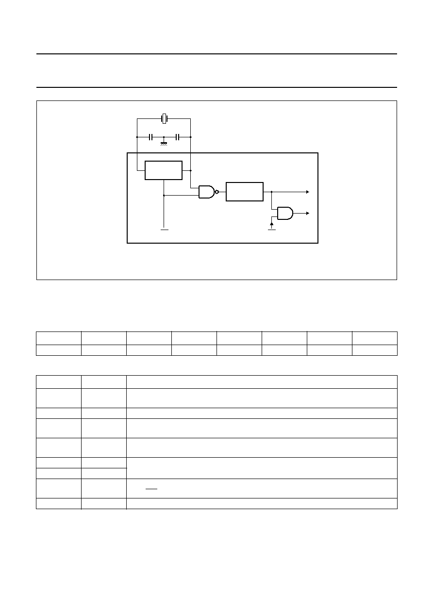
17 RESET CIRCUITRY
The reset circuitry for the P8xC562 is connected to the
reset pin RST. A Schmitt trigger is used at the input for
noise rejection. The output of the Schmitt trigger is
sampled by the reset circuitry every machine cycle.
The on-chip Reset circuit is shown in Fig.16.
A reset is accomplished by holding the RST pin HIGH for
at least two machine cycles (24 oscillator periods but at
least 2
µ
s). The CPU responds by executing an internal
reset. During reset both ALE and PSEN output a HIGH
level. In order to perform a correct reset, this level must not
be affected by external elements.
Also with the P8xC562, the RST line can be pulled HIGH
internally by a pull-up transistor activated by the Watchdog
Timer (T3). The length of the output pulse from the
Watchdog Timer is 3 machine cycles. A pulse of such
short duration is necessary in order to recover from a
processor or system fault as fast as possible.
It can be seen that the short reset pulse from T3 cannot
discharge the Power-on reset capacitor (see Fig.17).
Consequently, when the Watchdog Timer is also used to
reset external devices this capacitor arrangement should
not be connected to the RST pin, and an extra circuit
should be used to perform the Power-on-reset operation.
It should be remembered that a T3 overflow, if enabled, will
force a reset condition to the P8xC562 by an internal
connection, whether the output RST is tied LOW or not.
The internal reset is executed during the second cycle in
which RST is HIGH and is repeated every cycle until RST
goes LOW. The internal RAM is not affected by reset.
When V
DD
is turned on, the RAM content is indeterminate.
An internal reset leaves the internal registers as shown in
Table 36.
Fig.14 P8xC562P8xC562 oscillator circuit.
1) Use fundamental crystals only.
k, halfpage
C1
XTAL1
XTAL2
20 pF
C2
MBC751
20 pF
35
34
(1)
Fig.15 Driving the P8xC562 from an external source.
ook, halfpage
XTAL1
XTAL2
MGA169
external clock
(not TTL
compatible)
not connected
35
34
Fig.16 On-chip reset configuration.
andbook, halfpage
MBC476 - 1
SCHMITT
TRIGGER
RESET
CIRCUITRY
overflow
timer T3
VDD
RST
on-chip
resistor
RST
R

1997 Apr 08
31
Philips Semiconductors
Product specification
8-bit microcontroller
P83C562; P80C562
Table 36 State of internal registers after an internal reset
X = undefined state.
REGISTER
7
6
5
4
3
2
1
0
ACC
0
0
0
0
0
0
0
0
ADC0N
X
X
0
0
0
0
0
0
ADCH
X
X
X
X
X
X
X
X
B
0
0
0
0
0
0
0
0
CML0 to CML2
0
0
0
0
0
0
0
0
CMH0 to CMH2
0
0
0
0
0
0
0
0
CTCON
0
0
0
0
0
0
0
0
CTL0 to CTL3
X
X
X
X
X
X
X
X
CTH0 to CTH3
X
X
X
X
X
X
X
X
DPL
0
0
0
0
0
0
0
0
DPH
0
0
0
0
0
0
0
0
IEN0
0
0
0
0
0
0
0
0
IEN1
0
0
0
0
0
0
0
0
IP0
X
0
0
0
0
0
0
0
IP1
0
0
0
0
0
0
0
0
PCH
0
0
0
0
0
0
0
0
PCL
0
0
0
0
0
0
0
0
PCON
0
X
0
0
0
0
0
0
PSW
0
0
0
0
0
0
0
0
PWM0
0
0
0
0
0
0
0
0
PWM1
0
0
0
0
0
0
0
0
PWMP
0
0
0
0
0
0
0
0
P0 to P4
1
1
1
1
1
1
1
1
P5
X
X
X
X
X
X
X
X
RTE
0
0
0
0
0
0
0
0
SBUF
X
X
X
X
X
X
X
X
SCON
0
0
0
0
0
0
0
0
SP
0
0
0
0
0
1
1
1
STE
1
1
0
0
0
0
0
0
TCON
0
0
0
0
0
0
0
0
TH0, TH1
0
0
0
0
0
0
0
0
TMH2
0
0
0
0
0
0
0
0
TL0, TL1
0
0
0
0
0
0
0
0
TML2
0
0
0
0
0
0
0
0
TMOD
0
0
0
0
0
0
0
0
TM2CON
0
0
0
0
0
0
0
0
TM2IR
0
0
0
0
0
0
0
0
T3
0
0
0
0
0
0
0
0
17.1
Power-on-reset
When V
DD
is turned on, and provided its rise-time does not
exceed 10 ms, an automatic reset can be obtained by
connecting the RST pin to V
DD
via a 2.2
µ
F capacitor.
When the power is switched on, the voltage on the RST
pin, is equal to V
DD
minus the capacitor voltage, and
decreases from V
DD
as the capacitor charges through the
internal resistor (R
RST
) to ground. The larger the capacitor,
the more slowly V
RST
decreases. V
RST
must remain above
the lower threshold of the Schmitt trigger long enough to
effect a complete reset. The time required is the oscillator
start-up time, plus 2 machine cycles. The port pins will be
in a random state until the oscillator has started and the
internal reset algorithm has written logic 1s to the port pins.
The Power-on-reset circuitry is shown in Fig.17.
Fig.17 Power-on-reset.
handbook, halfpage
V
DD
V
DD
RST
2.2
µ
F
R RST
MBH344
8xC562

1997 Apr 08
32
Philips Semiconductors
Product specification
8-bit microcontroller
P83C562; P80C562
18 INSTRUCTION SET
The P8xC562 uses the powerful instruction set of the 80C51. Additional Special Function Registers are incorporated to
control the on-chip peripherals. The instruction set consists of 49 single-byte, 45 two-byte and 17 three-byte instructions.
When using a 16 MHz oscillator, 64 instructions execute in 0.75
µ
s and 45 instructions execute in 1.5
µ
s. Multiply and
divide instructions execute in 3
µ
s.
Tables 37 to 41 describe the Instruction set; Table 42 explains the Data addressing modes and the Hexadecimal
opcodes.
Table 37 Instruction set descriptions: Arithmetic operations
MNEMONIC
DESCRIPTION
BYTES
CYCLES
OPCODE
(HEX)
Arithmetic operations
ADD
A,Rr
Add register to A
1
1
2*
ADD
A,direct
Add direct byte to A
2
1
25
ADD
A,@Ri
Add indirect RAM to A
1
1
26, 27
ADD
A,#data
Add immediate data to A
2
1
24
ADDC
A,Rr
Add register to A with carry flag
1
1
3*
ADDC
A,direct
Add direct byte to A with carry flag
2
1
35
ADDC
A,@Ri
Add indirect RAM to A with carry flag
1
1
36, 37
ADDC
A,#data
Add immediate data to A with carry flag
2
1
34
SUBB
A,Rr
Subtract register from A with borrow
1
1
9*
SUBB
A,direct
Subtract direct byte from A with borrow
2
1
95
SUBB
A,@Ri
Subtract indirect RAM from A with borrow
1
1
96, 97
SUBB
A,#data
Subtract immediate data from A with borrow
2
1
94
INC
A
Increment A
1
1
04
INC
Rr
Increment register
1
1
0*
INC
direct
Increment direct byte
2
1
05
INC
@Ri
Increment indirect RAM
1
1
06, 07
DEC
A
Decrement A
1
1
14
DEC
Rr
Decrement register
1
1
1*
DEC
direct
Decrement direct byte
2
1
15
DEC
@Ri
Decrement indirect RAM
1
1
16, 17
INC
DPTR
Increment data pointer
1
2
A3
MUL
AB
Multiply A
&
B
1
4
A4
DIV
AB
Divide A by B
1
4
84
DA
A
Decimal adjust A
1
1
D4

1997 Apr 08
33
Philips Semiconductors
Product specification
8-bit microcontroller
P83C562; P80C562
Table 38 Instruction set description: Logic operations
MNEMONIC
DESCRIPTION
BYTES
CYCLES
OPCODE
(HEX)
Logic operations
ANL
A,Rr
AND register to A
1
1
5*
ANL
A,direct
AND direct byte to A
2
1
55
ANL
A,@Ri
AND indirect RAM to A
1
1
56, 57
ANL
A,#data
AND immediate data to A
2
1
54
ANL
direct,A
AND A to direct byte
2
1
52
ANL
direct,#data
AND immediate data to direct byte
3
2
53
ORL
A,Rr
OR register to A
1
1
4*
ORL
A,direct
OR direct byte to A
2
1
45
ORL
A,@Ri
OR indirect RAM to A
1
1
46, 47
ORL
A,#data
OR immediate data to A
2
1
44
ORL
direct,A
OR A to direct byte
2
1
42
ORL
direct,#data
OR immediate data to direct byte
3
2
43
XRL
A,Rr
Exclusive-OR register to A
1
1
6*
XRL
A,direct
Exclusive-OR direct byte to A
2
1
65
XRL
A,@Ri
Exclusive-OR indirect RAM to A
1
1
66, 67
XRL
A,#data
Exclusive-OR immediate data to A
2
1
64
XRL
direct,A
Exclusive-OR A to direct byte
2
1
62
XRL
direct,#data
Exclusive-OR immediate data to direct byte
3
2
63
CLR
A
Clear A
1
1
E4
CPL
A
Complement A
1
1
F4
RL
A
Rotate A left
1
1
23
RLC
A
Rotate A left through the carry flag
1
1
33
RR
A
Rotate A right
1
1
03
RRC
A
Rotate A right through the carry flag
1
1
13
SWAP
A
Swap nibbles within A
1
1
C4

1997 Apr 08
34
Philips Semiconductors
Product specification
8-bit microcontroller
P83C562; P80C562
Table 39 Instruction set description: Data transfer
MNEMONIC
DESCRIPTION
BYTES
CYCLES
OPCODE
(HEX)
Data transfer
MOV
A,Rr
Move register to A
1
1
E*
MOV
A,direct
Move direct byte to A
2
1
E5
MOV
A,@Ri
Move indirect RAM to A
1
1
E6, E7
MOV
A,#data
Move immediate data to A
2
1
74
MOV
Rr,A
Move A to register
1
1
F*
MOV
Rr,direct
Move direct byte to register
2
2
A*
MOV
Rr,#data
Move immediate data to register
2
1
7*
MOV
direct,A
Move A to direct byte
2
1
F5
MOV
direct,Rr
Move register to direct byte
2
2
8*
MOV
direct,direct
Move direct byte to direct byte
3
2
85
MOV
direct,@Ri
Move indirect RAM to direct byte
2
2
86, 87
MOV
direct,#data
Move immediate data to direct byte
3
2
75
MOV
@RI,A
Move A to indirect RAM
1
1
F6, F7
MOV
@Ri,direct
Move direct byte to indirect RAM
2
2
A6, A7
MOV
@Ri,#data
Move immediate data to indirect RAM
2
1
76, 77
MOV
DPTR,#data16
Load data pointer with a 16-bit constant
3
2
90
MOVC
A,@A+DPTR
Move code byte relative to DPTR to A
1
2
93
MOVC
A,@A+PC
Move code byte relative to PC to A
1
2
83
MOVX
A,@Ri
Move external RAM (8-bit address) to A
1
2
E2, E3
MOVX
A,@DPTR
Move external RAM (16-bit address) to A
1
2
E0
MOVX
@Ri,A
Move A to external RAM (8-bit address)
1
2
F2, F3
MOVX
@DPTR,A
Move A to external RAM (16-bit address)
1
2
F0
PUSH
direct
Push direct byte onto stack
2
2
C0
POP
direct
Pop direct byte from stack
2
2
D0
XCH
A,Rr
Exchange register with A
1
1
C*
XCH
A,direct
Exchange direct byte with A
2
1
C5
XCH
A,@Ri
Exchange indirect RAM with A
1
1
C6, C7
XCHD
A,@Ri
Exchange LOW-order nibble indirect RAM with A
1
1
D6, D7

1997 Apr 08
35
Philips Semiconductors
Product specification
8-bit microcontroller
P83C562; P80C562
Table 40 Instruction set description: Program and machine control
MNEMONIC
DESCRIPTION
BYTES
CYCLES
OPCODE
(HEX)
Program and machine control
ACALL
addr11
Absolute subroutine call
2
2
∑
1
LCALL
addr16
Long subroutine call
3
2
12
RET
Return from subroutine
1
2
22
RETI
Return from interrupt
1
2
32
AJMP
addr11
Absolute jump
2
2
1
LJMP
addr16
Long jump
3
2
02
SJMP
rel
Short jump (relative address)
2
2
80
JMP
@A+DPTR
Jump indirect relative to the DPTR
1
2
73
JZ
rel
Jump if A is zero
2
2
60
JNZ
rel
Jump if A is not zero
2
2
70
JC
rel
Jump if carry flag is set
2
2
40
JNC
rel
Jump if carry flag is not set
2
2
50
JB
bit,rel
Jump if direct bit is set
3
2
20
JNB
bit,rel
Jump if direct bit is not set
3
2
30
JBC
bit,rel
Jump if direct bit is set and clear bit
3
2
10
CJNE
A,direct,rel
Compare direct to A and jump if not equal
3
2
B5
CJNE
A,#data,rel
Compare immediate to A and jump if not equal
3
2
B4
CJNE
Rr,#data,rel
Compare immediate to reg. and jump if not equal
3
2
B*
CJNE
@Ri,#data,rel Compare immediate to ind. and jump if not equal
3
2
B6, B7
DJNZ
Rr,rel
Decrement register and jump if not zero
2
2
D*
DJNZ
direct,rel
Decrement direct and jump if not zero
3
2
D5
NOP
No operation
1
1
00

1997 Apr 08
36
Philips Semiconductors
Product specification
8-bit microcontroller
P83C562; P80C562
Table 41 Instruction set description: Boolean variable manipulation
Table 42 Description of the mnemonics in the instruction set
MNEMONIC
DESCRIPTION
BYTES
CYCLES
OPCODE
(HEX)
Boolean variable manipulation
CLR
C
Clear carry flag
1
1
C3
CLR
bit
Clear direct bit
2
1
C2
SETB
C
Set carry flag
1
1
D3
SETB
bit
Set direct bit
2
1
D2
CPL
C
Complement carry flag
1
1
B3
CPL
bit
Complement direct bit
2
1
B2
ANL
C,bit
AND direct bit to carry flag
2
2
82
ANL
C,/bit
AND complement of direct bit to carry flag
2
2
B0
ORL
C,bit
OR direct bit to carry flag
2
2
72
ORL
C,/bit
OR complement of direct bit to carry flag
2
2
A0
MOV
C,bit
Move direct bit to carry flag
2
1
A2
MOV
bit,C
Move carry flag to direct bit
2
2
92
MNEMONIC
DESCRIPTION
Data addressing modes
Rr
Working register R0-R7.
direct
128 internal RAM locations and any special function register (SFR).
@Ri
Indirect internal RAM location addressed by register R0 or R1 of the actual register bank.
#data
8-bit constant included in instruction.
#data 16
16-bit constant included as bytes 2 and 3 of instruction.
bit
direct addressed bit in internal RAM or SFR.
addr16
16-bit destination address. Used by LCALL and LJMP. The branch will be anywhere within the
64 kbytes program memory address space.
addr11
11-bit destination address. Used by ACALL and AJMP. The branch will be within the same 2 kbytes
page of program memory as the first byte of the following instruction.
rel
Signed (two's complement) 8-bit offset byte. Used by SJMP and all conditional jumps.
Range is
-
128 to +127 bytes relative to first byte of the following instruction.
Hexadecimal opcode cross-reference
*
8, 9, A, B, C, D, E, F.
∑
1, 3, 5, 7, 9, B, D, F.
0, 2, 4, 6, 8, A, C, E.

1997
Apr
08
37
Philips Semiconductors
Product specification
8-bit microcontroller
P83C562; P80C562
T
able 43
Instruction map
Note
1. MOV A, ACC is not a valid instruction.
First hexadecimal character of opcode
Second hexadecimal character of opcode
0
1
2
3
4
5
6
7
8
9
A B C D E F
0
NOP
AJMP
addr11
LJMP
addr16
RR
A
INC
A
INC
direct
INC @Ri
INC Rr
0
1
0
1
2
3
4
5
6
7
1
JBC
bit,rel
ACALL
addr11
LCALL
addr16
RRC
A
DEC
A
DEC
direct
DEC @Ri
DEC Rr
0
1
0
1
2
3
4
5
6
7
2
JB
bit,rel
AJMP
addr11
RET
RL
A
ADD
A,#data
ADD
A,direct
ADD A,@Ri
ADD A,Rr
0
1
0
1
2
3
4
5
6
7
3
JNB
bit,rel
ACALL
addr11
RETI
RLC
A
ADDC
A,#data
ADDC
A,direct
ADDC A,@Ri
ADDC A,Rr
0
1
0
1
2
3
4
5
6
7
4
JC
rel
AJMP
addr11
ORL
direct,A
ORL
direct,#data
ORL
A,#data
ORL
A,direct
ORL A,@Ri
ORL A,Rr
0
1
0
1
2
3
4
5
6
7
5
JNC
rel
ACALL
addr11
ANL
direct,A
ANL
direct,#data
ANL
A,#data
ANL
A,direct
ANL A,@Ri
ANL A,Rr
0
1
0
1
2
3
4
5
6
7
6
JZ
rel
AJMP
addr11
XRL
direct,A
XRL
direct,#data
XRL
A,#data
XRL
A,direct
XRL A,@Ri
XRL A,Rr
0
1
0
1
2
3
4
5
6
7
7
JNZ
rel
ACALL
addr11
ORL
C,bit
JMP
@A+DPTR
MOV
A,#data
MOV
direct,#data
MOV @Ri,#data
MOV Rr,#data
0
1
0
1
2
3
4
5
6
7
8
SJMP
rel
AJMP
addr11
ANL
C,bit
MOVC
A,@A+PC
DIV
AB
MOV
direct,direct
MOV direct,@Ri
MOV direct,Rr
0
1
0
1
2
3
4
5
6
7
9
MOV
DTPR,#data16
ACALL
addr11
MOV
bit,C
MOVC
A,@A+DPTR
SUBB
A,#data
SUBB
A,direct
SUBB A,@Ri
SUB A,Rr
0
1
0
1
2
3
4
5
6
7
A
ORL
C,/bit
AJMP
addr11
MOV
bit,C
INC
DPTR
MUL
AB
MOV @Ri,direct
MOV Rr,direct
0
1
0
1
2
3
4
5
6
7
B
ANL
C,/bit
ACALL
addr11
CPL
bit
CPL
C
CJNE
A,#data,rel
CJNE
A,direct,rel
CJNE @Ri,#data,rel
CJNE Rr,#data,rel
0
1
0
1
2
3
4
5
6
7
C
PUSH
direct
AJMP
addr11
CLR
bit
CLR
C
SWAP
A
XCH
A,direct
XCH A,@Ri
XCH A,Rr
0
1
0
1
2
3
4
5
6
7
D
POP
direct
ACALL
addr11
SETB
bit
SETB
C
DA
A
DJNZ
direct,rel
XCHD A,@Ri
DJNZ Rr,rel
0
1
0
1
2
3
4
5
6
7
E
MOVX
A,@DTPR
AJMP
addr11
MOVX A,@Ri
CLR
A
MOV
A,direct
(1)
MOV A,@Ri
MOV A,Rr
0
1
0
1
0
1
2
3
4
5
6
7
F
MOVX
@DTPR,A
ACALL
addr11
MOVX @Ri,A
CPL
A
MOV
direct,A
MOV @Ri,A
MOV Rr,A
0
1
0
1
0
1
2
3
4
5
6
7
1997 Apr 08
38
Philips Semiconductors
Product specification
8-bit microcontroller
P83C562; P80C562
19 LIMITING VALUES
In accordance with the Absolute Maximum Rating System (IEC 134).
20 DC CHARACTERISTICS
V
DD
= 5 V
±
10%; V
SS
= 0 V; all voltages with respect to V
SS
unless otherwise specified; f
OSC
= 16 MHz.
T
amb
=
-
40 to +85
∞
C for the P8xC562EFx.
SYMBOL
PARAMETER
MIN.
MAX.
UNIT
V
I
input voltage on any pin with respect to ground (V
SS
)
-
0.5
+6.5
V
I
I
, I
O
input, output DC current on any single I/O pin
-
5.0
mA
P
tot
total power dissipation
-
1.0
W
T
stg
storage temperature range
-
65
+150
∞
C
T
amb
operating ambient temperature range
P8xC562EBx
0
+70
∞
C
P8xC562EFx
-
40
+85
∞
C
P8xC562EHx
-
40
+125
∞
C
SYMBOL
PARAMETER
CONDITIONS
MIN.
MAX.
UNIT
Supply (digital part)
V
DD
supply voltage P8xC562Exx
4.5
5.5
V
I
DD
operating supply current
note 1
P8xC562Exx
-
40
mA
I
DD(ID)
supply current Idle mode
note 2
P8xC562Exx
-
9
mA
I
DD(PD)
supply current Power-down mode
note 3
P8X562EBx
2 V
<
V
DD(PD)
<
V
DD(max)
-
50
µ
A
P8X562EFx
2 V
<
V
DD(PD)
<
V
DD(max)
-
50
µ
A
P8X562EHx
2 V
<
V
DD(PD)
<
V
DD(max)
-
150
µ
A
Inputs
V
IL
LOW level input voltage (except EA)
-
0.5
0.2V
DD
-
0.1
V
V
IL1
LOW level input voltage (EA)
-
0.5
0.2V
DD
-
0.3
V
V
IH
HIGH level input voltage
(except RST, XTAL1)
0.2V
DD
+ 0.9 V
DD
+ 0.5
V
V
IH1
HIGH level input voltage
(RST and XTAL1)
0.7V
DD
V
DD
+ 0.5
V
I
IL
input current logic 0
Ports 1, 2, 3 and 4;
(except P1.6/SCL, P1.7/SDA)
V
I
= 0.45 V
-
-
50
µ
A
I
TL
input current HIGH-to-LOW transition
(Ports 1, 2, 3 and 4)
V
I
= 2.0 V
-
-
650
µ
A
I
LI1
input leakage current
(Port 0, EA, STADC, EW)
0.45 V
<
V
I
<
V
DD
-
±
10
µ
A
I
LI3
input leakage current (Port 5)
0.45 V
<
V
I
<
V
DD
-
±
1
µ
A

1997 Apr 08
39
Philips Semiconductors
Product specification
8-bit microcontroller
P83C562; P80C562
Outputs
V
OL
LOW level output voltage
(Ports 1, 2, 3 and 4)
I
OL
= 1.6 mA; note 4
-
0.45
V
V
OL1
LOW level output voltage
(Port 0, ALE, PSEN, PWM0, PWM1)
I
OL
= 3.2 mA; note 4
-
0.45
V
V
OH
HIGH level output voltage
Ports 1, 2, 3 and 4
I
OH
=
-
60
µ
A
2.4
-
V
I
OH
=
-
25
µ
A
0.75V
DD
-
V
I
OH
=
-
10
µ
A
0.9V
DD
-
V
V
OH1
HIGH level output voltage
Port 0 in external bus mode,
ALE, PSEN, PWM0, PWM1; note 5
I
OH
=
-
800
µ
A
2.4
-
V
I
OH
=
-
300
µ
A
0.75V
DD
-
V
I
OH
=
-
80
µ
A
0.9V
DD
-
V
V
OH2
HIGH level output voltage (RST)
I
OH
=
-
400
µ
A
2.4
-
V
I
OH
=
-
120
µ
A
0.8V
DD
-
V
R
RST
RST pull-down resistor
50
150
k
C
I/O
capacitance of I/O buffer
test frequency = 1 MHz;
T
amb
= 25
∞
C
-
10
pF
Supply (analog part)
V
DDA
supply voltage
V
DDA
= V
DD
±
0.2 V
4.5
5.5
V
P8X562Exx
I
DDA
supply current operating
Port 5 = 0 to V
DDA
1.2
mA
I
DDA(ID)
supply current Idle mode
P8X562EBx
-
50
µ
A
P8X562EFx
-
50
µ
A
P8X562EHx
-
100
µ
A
I
DDA(PD)
supply current Power-down mode
2 V
<
V
DDA(PD)
<
V
DDA(max)
P8X562EBx
-
50
µ
A
P8X562EFx
-
50
µ
A
P8X562EHx
-
100
µ
A
SYMBOL
PARAMETER
CONDITIONS
MIN.
MAX.
UNIT

1997 Apr 08
40
Philips Semiconductors
Product specification
8-bit microcontroller
P83C562; P80C562
Notes to the DC characteristics
1. The operating supply current is measured with all output pins disconnected;
XTAL1 driven with t
r
= t
f
= 10 ns; V
IL
= V
SS
+ 0.5 V; V
IH
= V
DD
-
0.5 V; XTAL2 not connected;
EA = RST = Port 0 = EW = V
DD
; STADC = V
SS
.
2. The Idle mode supply current is measured with all output pins disconnected;
XTAL1 driven with t
r
= t
f
= 10 ns; V
IL
= V
SS
+ 0.5 V; V
IH
= V
DD
-
0.5 V; XTAL2 not connected;
EA = Port 0 = EW = V
DD
; RST = STADC = V
SS
.
3. The Power-down current is measured with all output pins disconnected; XTAL2 not connected;
EA = Port 0 = EW = V
DD
; RST = STADC = XTAL1 = V
SS
.
4. Capacitive loading on Ports 0 and 2 may cause spurious noise pulses to be superimposed on the low level output
voltage of ALE and Ports 1, 3 and 4. The noise is due to external bus capacitance discharging into the Port 0 and
Port 2 pins when these pins make HIGH-to-LOW transitions during bus operations. In the most adverse condition
(capacitive loading
>
100 pF), the noise pulse on the ALE line may exceed 0.8 V. In such events it may be required
to qualify ALE with a Schmitt trigger, or use an address latch with a Schmitt trigger strobe input.
5. Capacitive loading on Ports 0 and 2 may cause the high level output voltage on ALE and PSEN to momentarily fall
below to 0.9V
DD
specification when the address bits are stabilizing.
6. V
REF+
= 5.12 V; V
REF
-
= 0 V; V
DDA
= 5.0 V.
7. The differential non-linearity (DL
e
) is the difference between the actual step width and the ideal step width.
8. The integral non-linearity (IL
e
) is the peak difference between the centre of the steps of the actual and the ideal
transfer curve after appropriate adjustment of gain and offset error.
9. The gain error (G
e
) is the relative difference in percent between the straight line fitting the actual transfer curve after
removing offset error, and the straight line which fits the ideal transfer curve. Gain error is constant at every point on
the transfer curve.
10. The offset error (OS
e
) is the absolute difference between the straight line which fits the actual transfer curve after
removing gain error, and a straight line which fits the ideal transfer curve. The offset error is constant at every point
of the actual transfer curve.
11. V
REF
-
= 0 V; V
DDA
= 5 V; V
REF+
= 5.12 V. The ADC is monotonic with no missing codes. Measurement by
continuously increasing V
IN
from
-
20 mV to 5.12 V in increments of 2 mV.
Analog inputs
V
IN
analog input voltage
AV
SS
-
0.2
AV
DD
+ 0.2
V
V
REF+
reference voltage (+)
-
AV
DD
+ 0.2
V
V
REF
-
reference voltage (
-)
AV
SS
-
0.2
-
V
R
REF
resistance between V
REF+
and V
REF
-
5
25
k
C
IA
analog input capacitance
-
15
pF
t
ADS
sampling time
-
6t
CY
µ
s
t
ADC
conversion time
(including sample time)
-
24t
CY
µ
s
DL
e
differential non-linearity
notes 7 and 11
-
±
1
LSB
IL
e
integral non-linearity
notes 6 and 8
-
±
1
LSB
OS
e
offset error
notes 6 and 10
-
±
1
LSB
G
e
gain error
notes 6 and 9
-
±
0.4
%
M
ctc
channel-to-channel matching
-
±
1
LSB
C
t
crosstalk between P5 inputs
0 to 100 kHz
-
-
60
dB
SYMBOL
PARAMETER
CONDITIONS
MIN.
MAX.
UNIT

1997 Apr 08
41
Philips Semiconductors
Product specification
8-bit microcontroller
P83C562; P80C562
Fig.18 Supply current (I
DD
, I
ID
) as a function of frequency at XTAL1 (f
osc
).
(1) I
DD(max)
operating mode; V
DD
= 5.5 V.
(2) I
DD(max)
operating mode; V
DD
= 4.5 V.
(3) I
ID(max)
Idle mode; V
DD
= 5.5V.
(4) I
ID(max)
Idle mode; V
DD
= 4.5 V.
These values are valid within the specified frequency range.
handbook, halfpage
0
4
8
16
50
0
40
MBC747
12
30
20
10
f (MHz)
(1)
(2)
(3)
(4)
(mA)
DD
I , I
ID

1997 Apr 08
42
Philips Semiconductors
Product specification
8-bit microcontroller
P83C562; P80C562
Fig.19 ADC conversion characteristic.
(1) Example of an actual transfer curve.
(2) The ideal transfer curve.
(3) Differential non-linearity (DL
e
).
(4) Integral non-linearity (IL
e
).
(5) Centre of a step of the actual transfer curve.
dbook, full pagewidth
MBH351
1
2
3
4
5
6
7
250 251 252
253 254 255
256
0
1
2
3
4
5
6
7
250
251
252
253
254
255
1 LSB ideal =
AVREF
+-
AVREF
-
1024
AV (LSB )
IN
ideal
code
out
offset error
OS
e
offset error OS e
gain error Ge
(2)
(3)
(4)
(5)
(1)
1 LSB (ideal)

1997 Apr 08
43
Philips Semiconductors
Product specification
8-bit microcontroller
P83C562; P80C562
21 AC CHARACTERISTICS
Parameters are valid over operating temperature range and operating supply voltage range unless otherwise specified.
C
L
= 100 pF for Port 0, ALE and PSEN; C
L
= 80 pF for all other outputs unless specified. See Figs 23 to 25.
Note
1. t
CLK
= 1/f
osc
= one oscillator clock period. If f
osc
= 16 MHz then t
CLK
= 62.5 ns.
SYMBOL
PARAMETER
f
OSC
= 16 MHz
f
OSC
= VARIABLE
UNIT
MIN.
MAX.
MIN.
MAX.
Program memory
t
LL
ALE pulse duration
85
-
2t
CLK
-
40
-
ns
t
AL
address set-up time to ALE
8
-
t
CLK
-
55
-
ns
t
LA
address hold time after ALE
28
-
t
CLK
-
35
-
ns
t
LIV
time from ALE to valid instruction input
-
150
-
4t
CLK
-
100
ns
t
LC
time from ALE to control pulse PSEN
23
-
t
CLK
-
40
-
ns
t
CC
control pulse duration PSEN
143
-
3t
CLK
-
45
-
ns
t
CIV
time from PSEN to valid instruction input
-
83
-
3t
CLK
-
105
ns
t
CI
input instruction hold time after PSEN
0
-
0
-
ns
t
CIF
input instruction float delay after PSEN
-
38
-
t
CLK
-
25
ns
t
AIV
address to valid instruction input
-
208
-
5t
CLK
-
105
ns
t
AFC
address float delay after PSEN
-
10
-
10
ns
External data memory
t
RR
RD pulse duration
275
-
6t
CLK
-
100
-
ns
t
WW
WR pulse duration
275
-
6t
CLK
-
100
-
ns
t
AL
address set-up time to ALE
8
-
t
CLK
-
55
-
ns
t
LA
address hold time after ALE
28
-
t
CLK
-
35
-
ns
t
RD
RD to valid data input
-
148
-
5t
CLK
-
165
ns
t
DR
data hold time after RD
0
-
0
-
ns
t
DFR
data float delay after RD
-
55
-
2t
CLK
-
70
ns
t
LD
time from ALE to valid data input
-
350
-
8t
CLK
-
150
ns
t
AD
address to valid data input
-
398
-
9t
CLK
-
165
ns
t
LW
time from ALE to RD or WR
138
238
3t
CLK
-
50
3t
CLK
+ 50
ns
t
AW
time from address to RD or WR
120
-
4t
CLK
-
130
-
ns
t
WHLH
time from RD or WR HIGH to ALE HIGH
23
103
t
CLK
-
40
t
CLK
+ 40
ns
t
DWX
data valid to WR transition
3
-
t
CLK
-
60
-
ns
t
DW
data set-up time before WR
288
-
7t
CLK
-
150
-
ns
t
WD
data hold time after WR
13
-
t
CLK
-
50
-
ns
t
AFR
address float delay after RD
-
0
-
0
ns

1997 Apr 08
44
Philips Semiconductors
Product specification
8-bit microcontroller
P83C562; P80C562
Fig.20 AC inputs test conditions.
handbook, full pagewidth
MLA753
(b)
(a)
timing reference
points
0.45 V
VLOAD
V 0.1 V
LOAD
V 0.1 V
LOAD
0.2 V 0.9
DD
V 0.5
DD
V 0.1 V
OL
0.2 V 0.1
DD
V 0.1 V
OH
AC inputs during testing are driven at V
DD
-
0.5 V for a logic 1, and 0.45 V for a logic 0.
Timing measurements are made at V
IH(min)
for a logic 1, and V
IL(max)
for a logic 0. See Fig.25 (a).
For timing purposes a port pin is no longer floating when a 100 mV change from load voltage occurs. A port pin begins to float when a
100 mV change from the loaded V
OH
/V
OL
level occurs. I
OL
/I
OH
±
20 mA (for testing purposes only). See Fig.25 (b).

1997 Apr 08
45
Philips Semiconductors
Product specification
8-bit microcontroller
P83C562; P80C562
Fig.21 Instruction cycle timing.
The Port 5 input buffers have a maximum propagation delay of 300 ns. As a result Port 5 sample time starts 300 ns in advance of state S5 and ends
when S5 has finished.
handbook, full pagewidth
MGA180
P1 P2
S1
P1 P2
S2
P1 P2
S3
P1 P2
S4
P1 P2
S5
P1 P2
S6
P1 P2
S1
P1 P2
S2
P1 P2
S3
P1 P2
S4
P1 P2
S5
P1 P2
S6
one machine cycle
one machine cycle
XTAL1
INPUT
address
A0 - A7
inst.
in
address
A0 - A7
inst.
in
address
A0 - A7
inst.
in
address
A0 - A7
inst.
in
address A8 - A15
address A8 - A15
address A8 - A15
address A8 - A15
address
A0 - A7
inst.
in
address
A0 - A7
inst.
in
address
A0 - A7
data output or data input
address A8 - A15
address A8 - A15 or Port 2 out
address A8 - A15
old data
new data
sampling time of I/O port pins during input (including INT0 and INT1)
SERIAL
PORT
CLOCK
PORT
INPUT
PORT
OUTPUT
PORT 2
BUS
(PORT 0)
read or
write of
external data
memory
PORT 2
BUS
(PORT 0)
external
program
memory
fetch
WR
RD
only active
during a write
to external
data memory
only active
during a read
from external
data memory
PSEN
ALE
dotted lines
are valid when
RD or WR are
active

1997 Apr 08
46
Philips Semiconductors
Product specification
8-bit microcontroller
P83C562; P80C562
Fig.22 Read from program memory.
handbook, full pagewidth
MGA176
t LHLL
ALE
PORT 0
PORT 2
t CY
LLIV
t
t LLPL
t PLPH
t LLAX
t AVLL
AVIV
t
PLAZ
t
PLIV
t
t PXIX
t PXIZ
address A8 to A15
address A8 to A15
inst. input
inst. input
A0 to A7
A0 to A7
PSEN
Fig.23 Read from data memory.
handbook, full pagewidth
MBC743
t LL
ALE
PORT 0
PORT 2
t CY
t LD
t LA
t AL
AD
t
AFR
t
address A8 to A15 or Port 2 out
data input
A0 to A7
PSEN
t WHLH
AW
t
t LW
t RR
t DR
t DFR
t RD
RD

1997 Apr 08
47
Philips Semiconductors
Product specification
8-bit microcontroller
P83C562; P80C562
Fig.24 Write to data memory.
ndbook, full pagewidth
MBC744
t LL
ALE
PORT 0
PORT 2
t CY
t LA
t AL
address A8 to A15 or special function registers (SFR)
data output
A0 to A7
PSEN
t WHLH
AW
t
t LW
t WW
t WD
t DW
t DWX
WR

1997 Apr 08
48
Philips Semiconductors
Product specification
8-bit microcontroller
P83C562; P80C562
Table 44 External clock drive XTAL1
Test conditions: operating temperature and supply voltage ranges; load capacitance = 80 pF.
Table 45 Serial timing - shift register mode using 16 MHz oscillator
SYMBOL
PARAMETER
MIN.
MAX.
UNIT
t
CLK
clock period
62.5
285.7
ns
t
HIGH
HIGH time
20
-
ns
t
LOW
LOW time
20
-
ns
t
r
rise time
-
20
ns
t
f
fall time
-
20
ns
t
CY
cycle time (12 t
CLK
)
0.75
3.43
µ
s
SYMBOL
PARAMETER
16 MHz OSC
VARIABLE OSCILLATOR
UNIT
MIN.
MAX.
MIN.
MAX.
t
XLXL
serial port clock cycle time
0.75
-
12t
CLK
-
µ
s
t
QVXH
output data set-up to clock rising edge
492
-
10t
CLK
-
133
-
ns
t
XHQX
output data hold after clock rising edge
8.0
-
2t
CLK
-
117
-
ns
t
XHDX
input data hold after clock rising edge
0
-
0
-
ns
t
XHDV
clock rising edge to input data valid
-
492
-
10t
CLK
-
133
ns
Fig.25 External clock drive XTAL.
handbook, full pagewidth
MBC479
t HIGH
t LOW
t CK
t r
t f
VIH1
V IH1
0.8 V
0.8 V
VIH1
VIH1
0.8 V
0.8 V
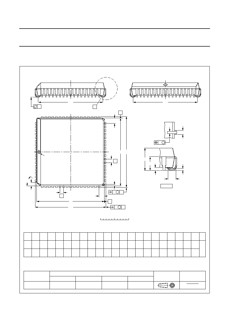
1997 Apr 08
49
Philips Semiconductors
Product specification
8-bit microcontroller
P83C562; P80C562
22 PACKAGE OUTLINE
REFERENCES
OUTLINE
VERSION
EUROPEAN
PROJECTION
ISSUE DATE
IEC
JEDEC
EIAJ
Note
1. Plastic or metal protrusions of 0.01 inches maximum per side are not included.
SOT188-2
44
60
68
1
9
10
26
43
27
61
detail X
(A )
3
b
p
w
M
A
1
A
A
4
L
p
b
1
k
1
k
X
y
e
E
B
D
H
E
H
v
M
B
D
Z D
A
Z E
e
v
M
A
pin 1 index
112E10
MO-047AC
0
5
10 mm
scale
92-11-17
95-03-11
PLCC68: plastic leaded chip carrier; 68 leads
SOT188-2
UNIT
A
A
min.
max.
max.
max. max.
1
A
4
b
p
E
(1)
(1)
(1)
e
H
E
Z
y
w
v
mm
4.57
4.19
0.51
3.30
0.53
0.33
0.021
0.013
1.27
0.51
2.16
45
o
0.18
0.10
0.18
DIMENSIONS (millimetre dimensions are derived from the original inch dimensions)
D
(1)
24.33
24.13
H
D
25.27
25.02
E
Z
2.16
D
b
1
0.81
0.66
k
1.22
1.07
k
1
0.180
0.165
0.020
0.13
A
3
0.25
0.01
0.05
0.020
0.085
0.007 0.004
0.007
L
p
1.44
1.02
0.057
0.040
0.958
0.950
24.33
24.13
0.958
0.950
0.995
0.985
25.27
25.02
0.995
0.985
e
E
e
D
23.62
22.61
0.930
0.890
23.62
22.61
0.930
0.890
0.085
0.032
0.026
0.048
0.042
E
e
inches
D
e

1997 Apr 08
50
Philips Semiconductors
Product specification
8-bit microcontroller
P83C562; P80C562
23 SOLDERING
23.1
Introduction
There is no soldering method that is ideal for all IC
packages. Wave soldering is often preferred when
through-hole and surface mounted components are mixed
on one printed-circuit board. However, wave soldering is
not always suitable for surface mounted ICs, or for
printed-circuits with high population densities. In these
situations reflow soldering is often used.
This text gives a very brief insight to a complex technology.
A more in-depth account of soldering ICs can be found in
our
"IC Package Databook" (order code 9398 652 90011).
23.2
Reflow soldering
Reflow soldering techniques are suitable for all PLCC
packages.
The choice of heating method may be influenced by larger
PLCC packages (44 leads, or more). If infrared or vapour
phase heating is used and the large packages are not
absolutely dry (less than 0.1% moisture content by
weight), vaporization of the small amount of moisture in
them can cause cracking of the plastic body. For more
information, refer to the Drypack chapter in our
"Quality
Reference Handbook" (order code 9397 750 00192).
Reflow soldering requires solder paste (a suspension of
fine solder particles, flux and binding agent) to be applied
to the printed-circuit board by screen printing, stencilling or
pressure-syringe dispensing before package placement.
Several techniques exist for reflowing; for example,
thermal conduction by heated belt. Dwell times vary
between 50 and 300 seconds depending on heating
method. Typical reflow temperatures range from
215 to 250
∞
C.
Preheating is necessary to dry the paste and evaporate
the binding agent. Preheating duration: 45 minutes at
45
∞
C.
23.3
Wave soldering
Wave soldering techniques can be used for all PLCC
packages if the following conditions are observed:
∑
A double-wave (a turbulent wave with high upward
pressure followed by a smooth laminar wave) soldering
technique should be used.
∑
The longitudinal axis of the package footprint must be
parallel to the solder flow.
∑
The package footprint must incorporate solder thieves at
the downstream corners.
During placement and before soldering, the package must
be fixed with a droplet of adhesive. The adhesive can be
applied by screen printing, pin transfer or syringe
dispensing. The package can be soldered after the
adhesive is cured.
Maximum permissible solder temperature is 260
∞
C, and
maximum duration of package immersion in solder is
10 seconds, if cooled to less than 150
∞
C within
6 seconds. Typical dwell time is 4 seconds at 250
∞
C.
A mildly-activated flux will eliminate the need for removal
of corrosive residues in most applications.
23.4
Repairing soldered joints
Fix the component by first soldering two diagonally-
opposite end leads. Use only a low voltage soldering iron
(less than 24 V) applied to the flat part of the lead. Contact
time must be limited to 10 seconds at up to 300
∞
C. When
using a dedicated tool, all other leads can be soldered in
one operation within 2 to 5 seconds between
270 and 320
∞
C.

1997 Apr 08
51
Philips Semiconductors
Product specification
8-bit microcontroller
P83C562; P80C562
24 DEFINITIONS
25 LIFE SUPPORT APPLICATIONS
These products are not designed for use in life support appliances, devices, or systems where malfunction of these
products can reasonably be expected to result in personal injury. Philips customers using or selling these products for
use in such applications do so at their own risk and agree to fully indemnify Philips for any damages resulting from such
improper use or sale.
Data sheet status
Objective specification
This data sheet contains target or goal specifications for product development.
Preliminary specification
This data sheet contains preliminary data; supplementary data may be published later.
Product specification
This data sheet contains final product specifications.
Limiting values
Limiting values given are in accordance with the Absolute Maximum Rating System (IEC 134). Stress above one or
more of the limiting values may cause permanent damage to the device. These are stress ratings only and operation
of the device at these or at any other conditions above those given in the Characteristics sections of this specification
is not implied. Exposure to limiting values for extended periods may affect device reliability.
Application information
Where application information is given, it is advisory and does not form part of the specification.

Internet: http://www.semiconductors.philips.com
Philips Semiconductors ≠ a worldwide company
© Philips Electronics N.V. 1997
SCA54
All rights are reserved. Reproduction in whole or in part is prohibited without the prior written consent of the copyright owner.
The information presented in this document does not form part of any quotation or contract, is believed to be accurate and reliable and may be changed
without notice. No liability will be accepted by the publisher for any consequence of its use. Publication thereof does not convey nor imply any license
under patent- or other industrial or intellectual property rights.
Netherlands: Postbus 90050, 5600 PB EINDHOVEN, Bldg. VB,
Tel. +31 40 27 82785, Fax. +31 40 27 88399
New Zealand: 2 Wagener Place, C.P.O. Box 1041, AUCKLAND,
Tel. +64 9 849 4160, Fax. +64 9 849 7811
Norway: Box 1, Manglerud 0612, OSLO,
Tel. +47 22 74 8000, Fax. +47 22 74 8341
Philippines: Philips Semiconductors Philippines Inc.,
106 Valero St. Salcedo Village, P.O. Box 2108 MCC, MAKATI,
Metro MANILA, Tel. +63 2 816 6380, Fax. +63 2 817 3474
Poland: Ul. Lukiska 10, PL 04-123 WARSZAWA,
Tel. +48 22 612 2831, Fax. +48 22 612 2327
Portugal: see Spain
Romania: see Italy
Russia: Philips Russia, Ul. Usatcheva 35A, 119048 MOSCOW,
Tel. +7 095 755 6918, Fax. +7 095 755 6919
Singapore: Lorong 1, Toa Payoh, SINGAPORE 1231,
Tel. +65 350 2538, Fax. +65 251 6500
Slovakia: see Austria
Slovenia: see Italy
South Africa: S.A. PHILIPS Pty Ltd., 195-215 Main Road Martindale,
2092 JOHANNESBURG, P.O. Box 7430 Johannesburg 2000,
Tel. +27 11 470 5911, Fax. +27 11 470 5494
South America: Rua do Rocio 220, 5th floor, Suite 51,
04552-903 S„o Paulo, S√O PAULO - SP, Brazil,
Tel. +55 11 821 2333, Fax. +55 11 829 1849
Spain: Balmes 22, 08007 BARCELONA,
Tel. +34 3 301 6312, Fax. +34 3 301 4107
Sweden: Kottbygatan 7, Akalla, S-16485 STOCKHOLM,
Tel. +46 8 632 2000, Fax. +46 8 632 2745
Switzerland: Allmendstrasse 140, CH-8027 ZÐRICH,
Tel. +41 1 488 2686, Fax. +41 1 481 7730
Taiwan: Philips Semiconductors, 6F, No. 96, Chien Kuo N. Rd., Sec. 1,
TAIPEI, Taiwan Tel. +886 2 2134 2865, Fax. +886 2 2134 2874
Thailand: PHILIPS ELECTRONICS (THAILAND) Ltd.,
209/2 Sanpavuth-Bangna Road Prakanong, BANGKOK 10260,
Tel. +66 2 745 4090, Fax. +66 2 398 0793
Turkey: Talatpasa Cad. No. 5, 80640 GÐLTEPE/ISTANBUL,
Tel. +90 212 279 2770, Fax. +90 212 282 6707
Ukraine: PHILIPS UKRAINE, 4 Patrice Lumumba str., Building B, Floor 7,
252042 KIEV, Tel. +380 44 264 2776, Fax. +380 44 268 0461
United Kingdom: Philips Semiconductors Ltd., 276 Bath Road, Hayes,
MIDDLESEX UB3 5BX, Tel. +44 181 730 5000, Fax. +44 181 754 8421
United States: 811 East Arques Avenue, SUNNYVALE, CA 94088-3409,
Tel. +1 800 234 7381
Uruguay: see South America
Vietnam: see Singapore
Yugoslavia: PHILIPS, Trg N. Pasica 5/v, 11000 BEOGRAD,
Tel. +381 11 625 344, Fax.+381 11 635 777
For all other countries apply to: Philips Semiconductors, Marketing & Sales Communications,
Building BE-p, P.O. Box 218, 5600 MD EINDHOVEN, The Netherlands, Fax. +31 40 27 24825
Argentina: see South America
Australia: 34 Waterloo Road, NORTH RYDE, NSW 2113,
Tel. +61 2 9805 4455, Fax. +61 2 9805 4466
Austria: Computerstr. 6, A-1101 WIEN, P.O. Box 213,
Tel. +43 1 60 101, Fax. +43 1 60 101 1210
Belarus: Hotel Minsk Business Center, Bld. 3, r. 1211, Volodarski Str. 6,
220050 MINSK, Tel. +375 172 200 733, Fax. +375 172 200 773
Belgium: see The Netherlands
Brazil: see South America
Bulgaria: Philips Bulgaria Ltd., Energoproject, 15th floor,
51 James Bourchier Blvd., 1407 SOFIA,
Tel. +359 2 689 211, Fax. +359 2 689 102
Canada: PHILIPS SEMICONDUCTORS/COMPONENTS,
Tel. +1 800 234 7381
China/Hong Kong: 501 Hong Kong Industrial Technology Centre,
72 Tat Chee Avenue, Kowloon Tong, HONG KONG,
Tel. +852 2319 7888, Fax. +852 2319 7700
Colombia: see South America
Czech Republic: see Austria
Denmark: Prags Boulevard 80, PB 1919, DK-2300 COPENHAGEN S,
Tel. +45 32 88 2636, Fax. +45 31 57 0044
Finland: Sinikalliontie 3, FIN-02630 ESPOO,
Tel. +358 9 615800, Fax. +358 9 61580920
France: 4 Rue du Port-aux-Vins, BP317, 92156 SURESNES Cedex,
Tel. +33 1 40 99 6161, Fax. +33 1 40 99 6427
Germany: Hammerbrookstraþe 69, D-20097 HAMBURG,
Tel. +49 40 23 53 60, Fax. +49 40 23 536 300
Greece: No. 15, 25th March Street, GR 17778 TAVROS/ATHENS,
Tel. +30 1 4894 339/239, Fax. +30 1 4814 240
Hungary: see Austria
India: Philips INDIA Ltd, Shivsagar Estate, A Block, Dr. Annie Besant Rd.
Worli, MUMBAI 400 018, Tel. +91 22 4938 541, Fax. +91 22 4938 722
Indonesia: see Singapore
Ireland: Newstead, Clonskeagh, DUBLIN 14,
Tel. +353 1 7640 000, Fax. +353 1 7640 200
Israel: RAPAC Electronics, 7 Kehilat Saloniki St, PO Box 18053,
TEL AVIV 61180, Tel. +972 3 645 0444, Fax. +972 3 649 1007
Italy: PHILIPS SEMICONDUCTORS, Piazza IV Novembre 3,
20124 MILANO, Tel. +39 2 6752 2531, Fax. +39 2 6752 2557
Japan: Philips Bldg 13-37, Kohnan 2-chome, Minato-ku, TOKYO 108,
Tel. +81 3 3740 5130, Fax. +81 3 3740 5077
Korea: Philips House, 260-199 Itaewon-dong, Yongsan-ku, SEOUL,
Tel. +82 2 709 1412, Fax. +82 2 709 1415
Malaysia: No. 76 Jalan Universiti, 46200 PETALING JAYA, SELANGOR,
Tel. +60 3 750 5214, Fax. +60 3 757 4880
Mexico: 5900 Gateway East, Suite 200, EL PASO, TEXAS 79905,
Tel. +9-5 800 234 7381
Middle East: see Italy
Printed in The Netherlands
457047/1200/01/pp52
Date of release: 1997 Apr 08
Document order number:
9397 750 02133