Document Outline
- GENERAL DESCRIPTION
- FEATURES
- ORDERING INFORMATION
- PIN CONFIGURATION, 20-PIN TSSOP PACKAGES
- FUNCTIONAL DESCRIPTION
- ABSOLUTE MAXIMUM RATINGS
- DC ELECTRICAL CHARACTERISTICS
- COMPARATOR (RTHERMC AND RREFC) ELECTRICAL CHARACTERISTICS
- AC ELECTRICAL CHARACTERISTICS
- PACKAGE OUTLINE
- REVISION HISTORY
- Data sheet status
- Definitions
- Disclaimers

Philips
Semiconductors
P82CF201
Low power, low price dual fan manager
Product data
Supersedes data of 2002 Nov 04
2002 Nov 18
INTEGRATED CIRCUITS

Philips Semiconductors
Product data
P82CF201
Low power, low price dual fan manager
2
2002 Nov 18
853≠2393 29207
GENERAL DESCRIPTION
The P82CF201 is a 20-pin single-chip dual digital fan controller
designed for use with brushless DC fan motors. A thermistor (or
temperature resistive sensor) connected to the R
thermC
input
provides the required resistance of 10K to 1.75 K
for 30% to 98%
PWM duty cycle.
With temperature less than 25
∞
C (thermistor resistance more than
10 K
) and THRESHOLD is set to LOW, the fan will be off. When
temperature rises above 25
∞
C (NTC thermistor at 10K or less), the
PWM turns the fan on. The P82CF201 features a Turn-on Delay for
a second fan when both fans have to turn-on. This reduces the
in-rush current and suppresses acoustic noise.
The P82CF201 also features fan fault sensing for enhancing system
protection and reliability. It detects the presence of a fan, when the
running fan fails or jams using the voltage on V
SENSE
pin and
asserts the fault signal. The fault condition also triggers the
maximum PWM applied to the running fan. The fault is also asserted
when the thermistor resistance is less than 1.5 K
(temperature is
over 76
∞
C).
FEATURES
∑
Temperature proportional fan speed control resulting in low
acoustic and longer fan life
∑
3.0 V to 5.5 V operating range
∑
Dual PWM fan drive
∑
Constant temperature monitoring ensure reliable motor start-up at
turn-on, coming out of fault condition, or following a transient fault
∑
Constant fan sensing protect against fan failure and fault condition
∑
Over temperature and fan fail output pin
∑
20 mA direct drive to LED indicators for fan power supply failure,
fan failure, overheat warning, no fan connect
∑
500 mS turn-on delay for the second fan when both fans have to
turn-on, reducing high surge current and noise
∑
On-chip power-on reset allows operation with no external
components
∑
The watchdog timer performs self-check and reset function
∑
On-chip oscillator allows operations with no external oscillator
components
∑
Supports low cost NTC thermistors (for PTC use P82CF202)
∑
Hysteresis control (when THRESHOLD pin is connected to
Vss/Ground) for resistance between 10K (25
∞
C) and 15K (20
∞
C)
during cooling to avoid unnecessary fan turning during cool down
∑
Constant cooling (when THRESHOLD pin is not connected or tied
to V
DD
) for resistance above 10K
∑
Maximum PWM is asserted when one fan fails, cooling the system
during fan failure
∑
20-pin TSSOP package.
ORDERING INFORMATION
Type number
Package
Name
Description
Thermistor Range
Version
P82CF201BDH
TSSOP20
plastic thin shrink small outline package; 20 leads; body width 4.4 mm
NTC ≠ 1.7 to 32 K
SOT360-1
PIN CONFIGURATION, 20-PIN TSSOP PACKAGES
SU01716
1
2
3
4
5
6
7
8
9
11
12
13
14
15
16
17
18
19
20
FAN1DRIVE
V
SENSE1
FAN2DRIVE
NC
V
SS
V
SENSE2
FAULT
NC
NC
NC
NC
THRESHOLD
R
thermC
R
refC
NC
V
DD
NC
R
thermC
DRIVE
NC
R
refC
DRIVE
10
P82CF201

Philips Semiconductors
Product data
P82CF201
Low power, low price dual fan manager
2002 Nov 18
3
su01717
RC CONTROL
RESISTANCE
MEASUREMENT
FAULT
DETECTION
WATCHDOG
RESET
PWM 1 & 2
R
refC
DRIVE
R
thermC
DRIVE
FAULT
V
SENSE2
V
SENSE1
FAN1DRIVE
FAN2DRIVE
R
refC
R
thermC
Figure 1. Functional Block Diagram.
FUNCTIONAL DESCRIPTION
PWM Description
The PWM controls the fan speed by comparing the thermistor
resistance to a reference resistance. This ratio translates into the
duty cycle of the PWM.
The PWM controls the fan speed proportionally to the thermistor
resistance. The 30Hz PWM duty cycle has resistance control range
from 10K to 1.75 K
(typical for NTC thermistor) for 30% to 98%
output duty cycle. The PWM pins drive a low cost PNP transistor to
give a good drive into the N-channel MOSFET as the low side
power switch element in the system. Example of drive circuits will be
shown Figure 4. This output has asymmetric complementary drive.
Since the system relies on PWM rather than linear power control,
the dissipation in the power switch is kept to a minimum. Generally,
very small devices (TO-92 or SOT package) will suffice.
500 mS Delay Turn-On Description
When temperatures rise above 25
∞
C and THRESHOLD is tied to
GND (NTC thermistor at 10K or less) for both fans, there is a turn-on
delay of 500 mS for the second fan. This reduces the inrush current
and suppresses acoustic noise.
Thermistor Measurement Description
A resistor can be measured using a comparator, which compares
the RC time of a known reference resistance with the RC time of an
unknown resistor value. Since the same capacitor and internal
voltage reference are used throughout, it results in a simple
calculation.
R
unknown
=
((RunknownChargingTime*Rreference)/RreferenceChargingTime)
The RC circuits are charged in sequence, until they reach an
internal voltage reference of 1.23 V.
The RC charging time is measured in the 256uSec - 65535uSec.
This range is divided up in 256 time increments. Values of R and C
have to be chosen so that it will be within that window.
The RC charging time of the reference resistor and thermistor are
measured. The thermistor value is calculated by comparing the RC
time of the Reference resistor and RC time of the thermistor.
R
thermistor
= ((RthermistorCTime*Rreference)/RreferenceCTime)

Philips Semiconductors
Product data
P82CF201
Low power, low price dual fan manager
2002 Nov 18
4
su01718
R
refC
DRIVE
R
thermC
DRIVE
R
refC
R
ref
INTERNAL V
ref
COMPARATOR
R
thermC
R
therm
Figure 2.
Fan Drive
Depending on the value of the thermistor, the fans will be driven by
MOSFET with a PWM signal.
When the thermistor resistance is higher than 10 K
and
THRESHOLD is set to "0" , the fan will be turned off.
However when the thermistor resistance is higher than 10 K
and
THRESHOLD is set to "0" , the fan will be driven by a 30% duty
cycle.
When the thermistor resistance is 10 K
, the fan will be driven by a
30% duty cycle PWM signal.
When the thermistor resistance is 1.7 K
, the fan will be driven by a
95% duty cycle PWM signal.
Any value in between is linear.
A Hysteresis with 30% PWM duty cycle (when THRESHOLD = 0) is
introduced to maintain constant cooling when the thermistor cools
from 10K (approx. 25
∞
C) to down 15K (approx. 20
∞
C). This reduces
on/off cycling for small temperature fluctuation.
When THRESHOLD is not connected or tied to "1", the fans will
have a 30% PWM duty cycle to maintain constant cooling whenever
power is applied.
In most application, the V
GS
(Gate-Source Turn-on voltage) of the
MOSFET is lower than the V
OH
(V
DD
-0.7) of the fan drive pins.
When the V
GS
of MOSFET is higher than V
OH
, a non-inverting
amplifier (for N-type MOSFet) is needed. For easy reference, this
circuit is shown in Figure 5.
su01719
30%
95%
98%
PWM
R
therm
1.7K
10K
15K
HYSTERESIS
(THRESHOLD = 0)
Figure 3.
Philips Semiconductors
Product data
P82CF201
Low power, low price dual fan manager
2002 Nov 18
5
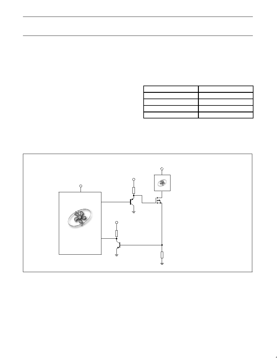
Motor Failure Detection and fault Reporting
(including watchdog reset)
As shown in Figure 4, the V
SENSE
input is connected to the collector
of NPN transistor through an inverting buffer transistor (2N3904 or
PMBT3904D) which amplifies the signal from the low-value current
sensing resistor in the ground return leg of the fan circuit. During
normal fan operation, communication occurs as each pole of the fan
is energized.
The fan current develops across the sense resistor(R
SENSE
). This a
voltage follower of the PWM pin.
In a running motor, a current will flow through the resistor R
SENSE
resulting in a voltage drop. The commutation will cause a narrow
window where there is no current flow. Motor detection is done by
the presence of commutation pulses. If there is constant voltage
level on the V
SENSE
pin when the motor is driven by a PWM signal,
the motor is jammed. When there is no voltage at all, the motor
might not be connected or the MOSFET is defective. The fault
condition also triggers the maximum PWM applied to the running
fan.
To detect the commutation pulses correctly, the V
SENSE
input needs
a logic high level of 0.2*V
DD
+0.9 V. (For example:
1.56 V@V
DD
=3.3 V). The design of proper sense circuitry is a
matter of scaling the R
SENSE
and the gain in buffer transistor to
meet the logic high as shown in Figure 4. Assuming the V
BE
(min) of
the transistor is approx. 0.5 V. Table 1 lists some recommended
R
SENSE
values according to the nominal operating current.
Table 1. Recommended values of R
SENSE
per
Figure 4
Nominal Fan Current(mA)
Min R
SENSE
(ohms)
100
5.1
200
2.5
450
2.2
800
1.0
In addition, when the thermistor resistance falls below 1.7 K
(for
NTC thermistor) indicating temperature above 76
∞
C, the fault line
will be asserted.
When the fan fails continuously, the fault signal will be held on LOW.
su01720
FANXDRIVE
V
SENSE
x
3.3 V
12 V FAN
+12 V
Q1
SI4410DY
R
SENSE
(2.2
TYPICAL)
+12 V
3.3 V
Figure 4. Interfacing the 82CF201 to a 2-Wire fan.

Philips Semiconductors
Product data
P82CF201
Low power, low price dual fan manager
2002 Nov 18
6
SU01722
1
2
3
4
5
6
7
8
9
11
12
13
14
15
16
17
18
19
20
10
3.3 V
3.3 V
R
ref
10 K
C 4.7
µ
F
R
therm
2.4 K
TYPICAL
12 V
12 V
V
SENSE2
FAN FAULT
V
SENSE1
FAN2 DRIVE
V
SENSE2
FAN
12 V
MOSFET2
V
SENSE1
12 V
MOSFET1
FAN1 DRIVE
FAN1
2-WIRE
FAN
FAN2
2-WIRE
FAN
D2 DIODE
D1 DIODE
2.2
R
SENSE2
3.3 V
3.3 V
2.2
R
SENSE1
FAN
2.4 K
TYPICAL
P82CF201
Figure 5. Typical application diagram.
su01721
Vref_Peak
0.5 sec
Figure 6. Waveform at Capacitor wrt Ground.

Philips Semiconductors
Product data
P82CF201
Low power, low price dual fan manager
2002 Nov 18
7
ABSOLUTE MAXIMUM RATINGS
PARAMETER
RATING
UNIT
Operating temperature under bias
≠55 to +125
∞
C
Storage temperature range
≠65 to +150
∞
C
Voltage on any other pin to V
SS
≠0.5 to 5.5 V
V
Maximum I
OL
per I/O pin
20
mA
Power dissipation (based on package heat transfer, not device power consumption)
1.5
W
NOTES:
1. Stresses above those listed under Absolute Maximum Ratings may cause permanent damage to the device. This is a stress rating only and
functional operation of the device at these or any conditions other than those described in the AC and DC Electrical Characteristics section
of this specification are not implied.
2. This product includes circuitry specifically designed for the protection of its internal devices from the damaging effects of excessive static
charge. Nonetheless, it is suggested that conventional precautions be taken to avoid applying greater than the rated maximum.
3. Parameters are valid over operating temperature range unless otherwise specified. All voltages are with respect to V
SS
unless otherwise
noted.
4. Parameters are valid over operating temperature range unless otherwise specified. All voltages are with respect to V
SS
unless otherwise
noted.
DC ELECTRICAL CHARACTERISTICS
V
DD
= 3.0 V to 5.5 V unless otherwise specified; T
amb
= 0
∞
C to +70
∞
C, unless otherwise specified
SYMBOL
PARAMETER
TEST CONDITIONS
LIMITS
UNIT
MIN
TYP
MAX
I
DD
Power supply current operating current
PWM =off, no fault
3.0 V < V
DD
< 5.5 V
2.2
5.5
mA
V
IL
Input LOW voltage (TTL input) all
Rsense
4.0 V < V
DD
< 5.5 V
≠0.5
0.2 V
DD
≠0.1
V
3.0 V < V
DD
< 4.0 V
≠0.5
0.7
V
V
IH
Input HIGH voltage (TTL input) all
Rsense
0.2 V
DD
+0.9
V
DD
+0.5
V
V
OL
Output LOW voltage all fan drive pins
I
OL
=3.2 mA, V
DD
=3.0 V
≠
0.4
V
V
OL1
Output LOW voltage all fan drive pins
I
OL
=20 mA, V
DD
=3.0 V
≠
1.0
V
V
OH
Output HIGH voltage all fan drive pins
I
OH
=-20
µ
A, V
DD
=3.0 V
V
DD
≠0.7 V
≠
V
I
OH
=-30
µ
A, V
DD
=4.5 V
V
DD
≠0.7 V
≠
V
V
OH1
Output HIGH voltage all fan drive pins
I
OH1
=-1.0 mA,
V
DD
=3.0 V
V
DD
≠0.7 V
≠
V
C
IO
Input/Output pin capacitance
≠
15
pF
I
IL
Logical 0 input current, all Rsense
V
IN
= 0.4 V
≠
-50
µ
A
I
LI
Input leakage current, all R
sense
,
R
thermC
, R
ThermDrive
, R
refC
and
R
refCDrive
V
IN
= V
IL
or V
IH
≠
±
2
µ
A
I
BOLOW
Brownout trip voltage with BOV=1
2.35
2.69
V
COMPARATOR (RTHERMC AND RREFC) ELECTRICAL CHARACTERISTICS
V
DD
= 3.0 V to 5.5 V unless otherwise specified; T
amb
= 0
∞
C to +70
∞
C, unless otherwise specified.
SYMBOL
PARAMETER
TEST CONDITIONS
LIMITS
UNIT
MIN
TYP
MAX
V
IO
Offset voltage comparator inputs
1
≠
±
10
mV
V
CR
Common mode range comparator
inputs
0
V
DD
≠0.3
V
I
IL
Input leakage current, comparator
0 < V
IN
< V
DD
≠
±
10
µ
A
NOTE:
1. This parameter is guaranteed by characterization but not tested in production.

Philips Semiconductors
Product data
P82CF201
Low power, low price dual fan manager
2002 Nov 18
8
AC ELECTRICAL CHARACTERISTICS
T
amb
= 0
∞
C to +70
∞
C, V
DD
= 3.0 V to 5.5 V unless otherwise specified; V
SS
= 0 V
1
SYMBOL
FIGURE
PARAMETER
LIMITS
UNIT
MIN
MAX
VRef_Peak
6
Charge_Peak at RefC and RthermC
1.1
1.55
V
PWM_DC
6
PWM Duty Cycle at fan drive Pin
30
98.4
%
NOTE:
1. Parameters are valid over operating temperature range unless otherwise specified.

Philips Semiconductors
Product data
P82CF201
Low power, low price dual fan manager
2002 Nov 18
9
TSSOP20:
plastic thin shrink small outline package; 20 leads; body width 4.4 mm
SOT360-1

Philips Semiconductors
Product data
P82CF201
Low power, low price dual fan manager
2002 Nov 18
10
REVISION HISTORY
Rev
Date
Description
_2
20021118
Product data (9397 750 10751); supersedes P82CF201_1 of 2002 Nov 04 (9397 750 10645)
Engineering Change Notice 853≠2393 29207 (date: 20021115)
Modifications:
∑
Corrected FET type number in Figure 4
_1
20021104
Product data (9397 750 10645); initial version.
Engineering Change Notice 853≠2393 29144 (date: 20021104).

Philips Semiconductors
Product data
P82CF201
Low power, low price dual fan manager
2002 Nov 18
11
Definitions
Short-form specification -- The data in a short-form specification is extracted from a full data sheet with the same type number and title. For detailed information see
the relevant data sheet or data handbook.
Limiting values definition -- Limiting values given are in accordance with the Absolute Maximum Rating System (IEC 60134). Stress above one or more of the limiting
values may cause permanent damage to the device. These are stress ratings only and operation of the device at these or at any other conditions above those given
in the Characteristics sections of the specification is not implied. Exposure to limiting values for extended periods may affect device reliability.
Application information -- Applications that are described herein for any of these products are for illustrative purposes only. Philips Semiconductors make no
representation or warranty that such applications will be suitable for the specified use without further testing or modification.
Disclaimers
Life support -- These products are not designed for use in life support appliances, devices, or systems where malfunction of these products can reasonably be
expected to result in personal injury. Philips Semiconductors customers using or selling these products for use in such applications do so at their own risk and agree
to fully indemnify Philips Semiconductors for any damages resulting from such application.
Right to make changes -- Philips Semiconductors reserves the right to make changes in the products--including circuits, standard cells, and/or software--described
or contained herein in order to improve design and/or performance. When the product is in full production (status `Production'), relevant changes will be communicated
via a Customer Product/Process Change Notification (CPCN). Philips Semiconductors assumes no responsibility or liability for the use of any of these products, conveys
no license or title under any patent, copyright, or mask work right to these products, and makes no representations or warranties that these products are free from patent,
copyright, or mask work right infringement, unless otherwise specified.
Contact information
For additional information please visit
http://www.semiconductors.philips.com.
Fax: +31 40 27 24825
For sales offices addresses send e-mail to:
sales.addresses@www.semiconductors.philips.com.
©
Koninklijke Philips Electronics N.V. 2002
All rights reserved. Printed in U.S.A.
Date of release: 11-02
Document order number:
9397 750 10751
Philips
Semiconductors
Data sheet status
[1]
Objective data
Preliminary data
Product data
Product
status
[2] [3]
Development
Qualification
Production
Definitions
This data sheet contains data from the objective specification for product development.
Philips Semiconductors reserves the right to change the specification in any manner without notice.
This data sheet contains data from the preliminary specification. Supplementary data will be published
at a later date. Philips Semiconductors reserves the right to change the specification without notice, in
order to improve the design and supply the best possible product.
This data sheet contains data from the product specification. Philips Semiconductors reserves the
right to make changes at any time in order to improve the design, manufacturing and supply. Relevant
changes will be communicated via a Customer Product/Process Change Notification (CPCN).
Data sheet status
[1] Please consult the most recently issued data sheet before initiating or completing a design.
[2] The product status of the device(s) described in this data sheet may have changed since this data sheet was published. The latest information is available on the Internet at URL
http://www.semiconductors.philips.com.
[3] For data sheets describing multiple type numbers, the highest-level product status determines the data sheet status.
Level
I
II
III