
DATA SHEET
Product specification
File under Integrated Circuits, IC20
1997 Dec 15
INTEGRATED CIRCUITS
P83C524; P80C528; P83C528
8-bit microcontrollers

1997 Dec 15
2
Philips Semiconductors
Product specification
8-bit microcontrollers
P83C524; P80C528;
P83C528
CONTENTS
1
FEATURES
2
GENERAL DESCRIPTION
3
QUICK REFERENCE DATA
4
ORDERING INFORMATION
5
BLOCK DIAGRAM
6
FUNCTIONAL DIAGRAM
7
PINNING INFORMATION
7.1
Pinning
7.2
Pin description
8
FUNCTIONAL DESCRIPTION
8.1
General
8.2
Instruction Set Execution
9
MEMORY ORGANIZATION
9.1
Program Memory
9.2
Internal Data Memory
9.3
Addressing
10
I/O FACILITIES
11
TIMERS/COUNTERS
11.1
Timer 0 and Timer 1
11.1.1
Timer/Counter Mode Control register (TMOD)
11.1.2
Timer/Counter Control Register (TCON)
11.2
Timer 2
11.2.1
Timer 2 Control Register (T2CON)
11.2.2
Capture Mode
11.2.3
Automatic Reload Mode
11.2.4
Baud Rate Generator Mode
11.3
Watchdog Timer T3
12
SERIAL PORT (UART)
12.1
Serial Port Control Register (SCON)
12.2
SM0 and SM1 operating modes (SCON)
13
BIT-LEVEL I
2
C INTERFACE
13.1
I
2
C Interrupt Register (S1INT)
13.2
Single-bit Data Register with I
2
C Auto-clock
(S1BIT)
13.2.1
Reading or Writing the S1BIT SFR
13.3
Control and Status Register for the I
2
C-bus
(S1SCS)
14
INTERRUPT SYSTEM
14.1
Interrupt Enable Register (IE)
14.2
Interrupt Priority Register (IP)
14.3
Interrupt Vectors
15
IDLE AND POWER-DOWN OPERATION
15.1
Power Control Register (PCON)
15.2
Idle Mode
15.3
Power-down Mode
15.4
Wake-up from Power-down Mode
16
OSCILLATOR CIRCUIT
17
RESET CIRCUIT
17.1
Power-on reset
18
INSTRUCTION SET
19
LIMITING VALUES
20
DC CHARACTERISTICS
21
AC CHARACTERISTICS
21.1
AC Characteristics 16 MHz version
21.2
AC Characteristics 24 MHz version
22
I
2
C CHARACTERISTICS (BIT-LEVEL)
23
XTAL1 CHARACTERISTICS
24
SERIAL PORT CHARACTERISTICS
25
TIMING DIAGRAMS
25.1
Timing symbol definitions
26
PACKAGE OUTLINES
27
SOLDERING
27.1
Introduction
27.2
DIP
27.2.1
Soldering by dipping or by wave
27.2.2
Repairing soldered joints
27.3
PLCC and QFP
27.3.1
Reflow soldering
27.3.2
Wave soldering
27.3.3
Repairing soldered joints
28
DEFINITIONS
29
LIFE SUPPORT APPLICATIONS
30
PURCHASE OF PHILIPS I
2
C COMPONENTS

1997 Dec 15
3
Philips Semiconductors
Product specification
8-bit microcontrollers
P83C524; P80C528; P83C528
1
FEATURES
∑
80C51 CPU
∑
32 kbytes on-chip ROM, expandable externally to
64 kbytes Program Memory address space
∑
P83C524:
≠ 16 kbytes on-chip ROM, expandable externally from
32 kbytes to 64 kbytes Program Memory address
space (address space 16 k to 32 k not usable)
∑
P80C528:
≠ ROMless version of P83C528
∑
P83C528:
≠ 32 kbytes on-chip ROM, expandable externally from
32 kbytes to 64 kbytes Program Memory address
space
∑
EPROM versions are available: see separate data sheet
P87C524 and P87C528
∑
512 bytes on-chip RAM, expandable externally to
64 kbytes Data Memory address space
∑
Four 8-bit I/O ports
∑
Full-duplex UART compatible with the standard 80C51
and the 8052
∑
Two standard 16-bit timer/counters
∑
An additional 16-bit timer (functionally equivalent to the
timer 2 of the 8052)
∑
On-chip Watchdog Timer (WDT) with an own oscillator
∑
Bit-level I
2
C-bus hardware serial I/O Port
∑
7-source and 7-vector interrupt structure with 2 priority
levels
∑
Up to 3 external interrupt request inputs
∑
Two programmable power reduction modes (Idle and
Power-down)
∑
Termination of Idle mode by any interrupt, external or
WDT (watchdog) reset
∑
Wake-up from Power-down by external interrupt,
external or WDT reset
∑
ROM code protection
∑
XTAL frequency range: 3.5 MHz to 16 MHz and
3.5 MHz to 24 MHz
∑
All packaging pin-outs fully compatible to the standard
8051/8052.
2
GENERAL DESCRIPTION
The P83C524 and P83C528 single-chip 8-bit
microcontrollers are manufactured in an advanced CMOS
process and are derivatives of the PCB80C51
microcontroller family. These devices provide architectural
enhancements that make them applicable in a variety of
applications in general control systems, especially in those
systems which need a large ROM and RAM capacity on
chip.
The P83C524 and P83C528 contain a non-volatile
16 k
◊
8 respectively 32 k
◊
8 read-only program memory,
a volatile 512 bytes
◊
8 read/write data memory, four 8-bit
I/O ports, two 16-bit timer/event counters (identical to the
timers of the 80C51), a 16-bit timer (identical to the timer 2
of the 8052), a multi-source, two-priority-level, nested
interrupt structure, two serial interfaces (UART and
bit-level I
2
C-bus), a watchdog timer (WDT) with a separate
oscillator, an on-chip oscillator and timing circuits. For
systems that require extra capability, the P83C524 and
P83C528 can be expanded using standard TTL
compatible memories and logic.
The device also functions as an arithmetic processor
having facilities for both binary and BCD arithmetic plus
bit-handling capabilities. The P83C524 and P83C528
have the same instruction set as the PCB80C51 which
consists of over 100 instructions: 49 one-byte, 46 two-byte
and 16 three-byte. With a 16 MHz crystal, 58% of the
instructions are executed in 750 ns and 40% in 1.5
µ
s.
Multiply and divide instructions require 3
µ
s.

1997 Dec 15
4
Philips Semiconductors
Product specification
8-bit microcontrollers
P83C524; P80C528; P83C528
3
QUICK REFERENCE DATA
4
ORDERING INFORMATION
SYMBOL
PARAMETER
CONDITION
MIN.
MAX.
UNIT
P83C524, P80C528, P83C528 (see characteristics tables for extended temperature range versions)
V
DD
supply voltage range
4.5
5.5
V
I
DD
supply current: operating modes 16 MHz
V
DD
= 5.5 V, f
CLK
= 16 MHz
-
33
mA
I
ID
supply current: Idle mode 16 MHz
V
DD
= 5.5 V, f
CLK
= 16 MHz
-
6
mA
I
PD
supply current: Power-down mode
2V
V
PD
V
DD
max.
-
100
µ
A
P
tot
total power dissipation
-
1
W
T
stg
storage temperature range
-
65
+150
∞
C
T
amb
operating ambient temperature range
-
40
+85
∞
C
EXTENDED
TYPE NUMBER
PACKAGE
TEMPERATURE
RANGE (
∞
C)
FREQ.
(MHZ)
NAME
DESCRIPTION
VERSION
ROMless
P80C528EBP
DIP40
plastic dual in-line package;
40 leads (600 mil)
SOT129-1
0 to +70
3.5 to 16
P80C528EFP
-
40 to +85
P80C528IBP
0 to +70
3.5 to 24
P80C528IFP
-
40 to +85
P80C528EBA
PLCC44
plastic leaded chip carrier; 44 leads
SOT187-2
0 to +70
3.5 to 16
P80C528EFA
-
40 to +85
P80C528IBA
0 to +70
3.5 to 24
P80C528IFA
-
40 to +85
P80C528EBB
QFP44
plastic quad flat package;
44 leads (lead length 1.3 mm);
body 10
◊
10
◊
1.75 mm
SOT307-2
0 to +70
3.5 to 16
P80C528EFB
-
40 to +85
P80C528IBB
0 to +70
3.5 to 24
P80C528IFB
-
40 to +85
ROM
P83C524EBP
DIP40
plastic dual in-line package;
40 leads (600 mil)
SOT129-1
0 to +70
3.5 to 16
P83C524EFP
-
40 to +85
P83C524IBP
0 to +70
3.5 to 24
P83C524IFP
-
40 to +85
P83C524EBA
PLCC44
plastic leaded chip carrier; 44 leads
SOT187-2
0 to +70
3.5 to 16
P83C524EFA
-
40 to +85
P83C524IBA
0 to +70
3.5 to 24
P83C524IFA
-
40 to +85
P83C524EBB
QFP44
plastic quad flat package;
44 leads (lead length 1.3 mm);
body 10
◊
10
◊
1.75 mm
SOT307-2
0 to +70
3.5 to 16
P83C524EFB
-
40 to +85
P83C524IBB
0 to +70
3.5 to 24
P83C524IFB
-
40 to +85

1997 Dec 15
5
Philips Semiconductors
Product specification
8-bit microcontrollers
P83C524; P80C528; P83C528
P83C528EBP
DIP40
plastic dual in-line package;
40 leads (600 mil)
SOT129-1
0 to +70
3.5 to 16
P83C528EFP
-
40 to +85
P83C528IBP
0 to +70
3.5 to 24
P83C528IFP
-
40 to +85
P83C528EBA
PLCC44
plastic leaded chip carrier; 44 leads
SOT187-2
0 to +70
3.5 to 16
P83C528EFA
-
40 to +85
P83C528IBA
0 to +70
3.5 to 24
P83C528IFA
-
40 to +85
P83C528EBB
QFP44
plastic quad flat package;
44 leads (lead length 1.3 mm);
body 10
◊
10
◊
1.75 mm
SOT307-2
0 to +70
3.5 to 16
P83C528EFB
-
40 to +85
P83C528IBB
0 to +70
3.5 to 24
P83C528IFB
-
40 to +85
EXTENDED
TYPE NUMBER
PACKAGE
TEMPERATURE
RANGE (
∞
C)
FREQ.
(MHZ)
NAME
DESCRIPTION
VERSION

1997
Dec
15
6
Philips Semiconductors
Product specification
8-bit microcontrollers
P83C524; P80C528; P83C528
This text is here in white to force landscape pages to be rotated correctly when browsing through the pdf in the Acrobat reader.This text is here in
_
white to force landscape pages to be rotated correctly when browsing through the pdf in the Acrobat reader.This text is here inThis text is here in
white to force landscape pages to be rotated correctly when browsing through the pdf in the Acrobat reader. white to force landscape pages to be ...
5
BLOCK DIAGRAM
handbook, full pagewidth
PROGRAMMABLE I/O
64K-BYTE BUS
EXPANSION
CONTROL
OSCILLATOR
AND
TIMING
CPU
internal
interrupts
PROGRAM
MEMORY
(32 K x 8 ROM/
EPROM)
DATA
MEMORY
(256 x 8 RAM)
PROGRAMMABLE
SERIAL PORT
FULL DUPLEX UART
SYNCHRONOUS
SHIFT
TWO 16-BIT
TIMER/EVENT
COUNTERS
XTAL2
XTAL1
frequency
reference
T0
T1
counters
external interrupts
control
parallel ports,
address/data bus
and I/O pins
serial in
serial out
INT1
INT0
MBC455
DATA
MEMORY
(256 x 8 RAM)
16-BIT
TIMER
WATCHDOG
TIMER
T2
T2EX
RST
BIT-LEVEL
INTERFACE
I C
2
AUX - RAM
RAM
shared with Port 3
SDA
SCL
Fig.1 Block diagram.
PROGRAM
MEMORY
(32 K x 8 ROM
or 16 K x 8 ROM)
P83C524
P80C528
P83C528

1997 Dec 15
7
Philips Semiconductors
Product specification
8-bit microcontrollers
P83C524; P80C528; P83C528
6
FUNCTIONAL DIAGRAM
Fig.2 Functional diagram.
handbook, full pagewidth
Port 0
address and
data bus
address bus
Port 1
Port 2
SCL
SDA
RST
XTAL1
XTAL2
ALE
EA
PSEN
Port 3
RXD / data
TXD / clock
T0
T1
INT0
INT1
WR
RD
alternative
functions
P83C528
MBC454 - 1
T2
T2EX
VDD
VSS
P83C524
P80C528
P83C528

1997 Dec 15
8
Philips Semiconductors
Product specification
8-bit microcontrollers
P83C524; P80C528; P83C528
7
PINNING INFORMATION
7.1
Pinning
Fig.3 Pin configuration DIP40 (SOT129-1).
handbook, halfpage
1
2
3
4
5
6
7
8
9
10
11
12
13
40
39
38
37
36
35
34
33
32
31
30
29
28
27
14
15
16
17
18
19
20
21
22
23
24
25
26
T2 P1.0
T2EX P1.1
P1.2
P1.3
P1.4
P1.5
SCL P1.6
SDA P1.7
RST
RXD / data P3.0
TXD / clock P3.1
T0 P3.4
T1 P3.5
XTAL2
XTAL1
VSS
VDD
P0.0 AD0
P0.1 AD1
P0.2 AD2
P0.3 AD3
P0.4 AD4
P0.5 AD5
P0.6 AD6
P0.7 AD7
ALE
P2.7 A15
P2.6 A14
P2.5 A13
P2.4 A12
P2.3 A11
P2.2 A10
P2.1 A9
P2.0 A8
P83C528
INT0 P3.2
INT1 P3.3
WR P3.6
RD P3.7
PSEN
MBC453
EA
P83C524
P80C528
P83C528

1997 Dec 15
9
Philips Semiconductors
Product specification
8-bit microcontrollers
P83C524; P80C528; P83C528
Fig.4 Pin configuration QFP44 (SOT307-2).
handbook, full pagewidth
7
8
9
10
11
12
13
14
15
16
17
39
38
37
36
35
34
33
32
31
30
29
18
19
20
21
22
23
24
25
26
27
28
6
5
4
3
2
1
44
43
42
41
40
P1.4
P1.3
P1.2
P1.1 / T2EX
P1.0 / T2
n.c.
V
DD
P0.0 / AD0
P0.1 / AD1
P0.2 / AD2
P0.3 / AD3
P0.4 / AD4
P0.5 / AD5
P0.6 / AD6
P0.7 / AD7
n.c.
ALE
P2.7 / A15
P2.6 / A14
P2.5 / A13
EA
PSEN
P1.5
SCL / P1.6
SDA / P1.7
RST
RXD / data / P3.0
n.c.
TXD / clock / P3.1
T0 / P3.4
T1 / P3.5
INT0 / P3.2
INT1 / P3.3
XTAL2
XTAL1
V
SS
n.c.
P2.0 / A8
P2.1 / A9
P2.2 / A10
P2.3 / A11
P2.4 / A12
WR / P3.6
RD / P3.7
P83C528
MBC452
1
2
8
7
6
5
4
3
9
10
11
12
14
15
16
17
18
19
13
20
21
22
27
26
25
24
23
28
29
30
31
32
33
35
34
36
37
38
39
40
41
42
43
44
P83C524
P80C528
P83C528

1997 Dec 15
10
Philips Semiconductors
Product specification
8-bit microcontrollers
P83C524; P80C528; P83C528
Fig.5 Pin configuration PLCC44 (SOT187-2).
handbook, full pagewidth
7
8
9
10
11
12
13
14
15
16
17
39
38
37
36
35
34
33
32
31
30
29
18
19
20
21
22
23
24
25
26
27
28
6
5
4
3
2
1
44
43
42
41
40
P1.4
P1.3
P1.2
P1.1 / T2EX
P1.0 / T2
n.c.
V
DD
P0.0 / AD0
P0.1 / AD1
P0.2 / AD2
P0.3 / AD3
P0.4 / AD4
P0.5 / AD5
P0.6 / AD6
P0.7 / AD7
n.c.
ALE
P2.7 / A15
P2.6 / A14
P2.5 / A13
EA
PSEN
P1.5
SCL / P1.6
SDA / P1.7
RST
RXD / data / P3.0
n.c.
TXD / clock / P3.1
T0 / P3.4
T1 / P3.5
INT0 / P3.2
INT1 / P3.3
XTAL2
XTAL1
V
SS
n.c.
P2.0 / A8
P2.1 / A9
P2.2 / A10
P2.3 / A11
P2.4 / A12
WR / P3.6
RD / P3.7
P83C528
MBC452
P83C524
P80C528
P83C528

1997 Dec 15
11
Philips Semiconductors
Product specification
8-bit microcontrollers
P83C524; P80C528; P83C528
7.2
Pin description
Table 1
Pin description for P83C524, P80C528 and P83C528; see note 1
SYMBOL
PIN
DESCRIPTION
SOT 129-1 SOT 187-2 SOT 307-2
P1.0
-
P1.7 1 to 8
2
-
9
(1 n.c.)
1
-
3,
40
-
44
(39 n.c.)
Port 1: 8-bit quasi-bidirectional I/O Port. Port 1 can sink/source
one TTL (= 4 LSTTL) input. It can drive CMOS inputs without
external pull-ups, except P1.6 and P1.7 which have open drain
outputs.
Port 1 alternative functions:
T2
1
2
40
P1.0
Timer/event counter 2 external event counter input
(falling edge triggered)
T2EX
2
3
41
P1.1
Timer/event counter 2 capture/reload trigger or external
interrupt 2 input (falling edge triggered)
SCL
7
8
2
P1.6
I
2
C-bus Serial Port clock line
SDA
8
9
3
P1.7
I
2
C-bus Serial Port data line.
RST
9
10
4
RESET: a HIGH level on this pin for two machine cycles while the
oscillator is running, resets the device. An internal pull-down
resistor permits power-on reset using only a capacitor connected
to V
DD
. After a WDT overflow this pin is pulled HIGH while the
internal reset signal is active.
P3.0
-
P3.7 10
-
17
11, 13
-
19
(12 n.c.)
5, 7
-
13
(6 n.c.)
Port 3: 8-bit quasi-bidirectional I/O Port with internal pull-ups.
Port 3 can sink/source one TTL (= 4 LSTTL) input. It can drive
CMOS inputs without external pull-ups.
Port 3 alternative functions:
RXD/data
10
11
5
P3.0
Serial Port data input (asynchronous) or data
input/output (synchronous)
TXD/clock
11
13
7
P3.1
Serial Port data output (asynchronous) or clock output
(synchronous)
INT0
12
14
8
P3.2
external interrupt 0 or gate control input for timer/event
counter 0
INT1
13
15
9
P3.3
external interrupt 1 or gate control input for timer/event
counter 1
T0
14
16
10
P3.4
external input for timer/event counter 0
T1
15
17
11
P3.5
external input for timer/event counter 1
WR
16
18
12
P3.6
external data memory write strobe
RD
17
19
13
P3.7
external data memory read strobe.
The generation or use of a Port 3 pin as an alternative function is
carried out automatically by the P83C528 provided the associated
Special Function Register (SFR) bit is set HIGH.
XTAL2
18
20
14
Crystal input 2: output of the inverting amplifier that forms the
oscillator. This pin left open-circuit when an external oscillator
clock is used (see Figures 22 and 23).

1997 Dec 15
12
Philips Semiconductors
Product specification
8-bit microcontrollers
P83C524; P80C528; P83C528
Note
1. To avoid a 'latch-up' effect at power-on, the voltage on any pin (at any time) must not be higher than V
DD
+0.5 V or
lower than V
SS
-
0.5 V respectively.
XTAL1
19
21
15
Crystal input 1: input to the inverting amplifier that forms the
oscillator, and input to the internal clock generator. Receives the
external oscillator clock signal when an external oscillator is used
(see Figures 22 and 23).
V
SS
20
22
16
Ground: circuit ground potential.
P2.0-P2.7
21
-
28
24
-
31
(23 n.c.)
18
-
25
(17 n.c.)
Port 2: 8-bit quasi-bidirectional I/O Port with internal pull-ups.
During access to external memories (RAM/ROM) that use 16-bit
addresses (MOVX @DPTR) Port 2 emits the high-order address
byte (A8 to A15). Port 2 can sink/source one TTL (= 4 LSTTL)
input. It can drive CMOS inputs without external pull-ups.
PSEN
29
32
26
Program Store Enable output: read strobe to the external
program memory via Port 0 and Port 2. It is activated twice each
machine cycle during fetches from external program memory.
When executing out of external program memory two activations of
PSEN are skipped during each access to external data memory.
PSEN is not activated (remains HIGH) during no fetches from
external program memory. PSEN can sink/source 8 LSTTL inputs.
It can drive CMOS inputs without external pull-ups.
ALE
30
33
27
Address Latch Enable output: latches the LOW byte of the
address during access to external memory in normal operation. It
is activated every six oscillator periods except during an external
data memory access. ALE can sink/source 8 LSTTL inputs. It can
drive CMOS inputs without an external pull-up.
EA
31
35
(34 n.c.)
29
(28 n.c.)
External Access input: when during RESET, EA is held at a TTL
HIGH level, the CPU executes out of the internal program ROM,
provided the program counter is less than 32768. When EA is held
at a TTL LOW level during RESET, the CPU executes out of
external program memory via Port 0 and Port 2. EA is not allowed
to float.
P0.0-P0.7
32
-
39
36
-
43
30
-
37
Port 0: 8-bit open drain bidirectional I/O Port. It is also the
multiplexed low-order address and data bus during accesses to
external memory (AD0 to AD7). During these accesses internal
pull-ups are activated. Port 0 can sink/source 8 LSTTL inputs.
V
DD
40
44
38
Power supply: +5 V power supply pin during normal operation,
Idle mode and Power-down mode.
SYMBOL
PIN
DESCRIPTION
SOT 129-1 SOT 187-2 SOT 307-2
1997 Dec 15
13
Philips Semiconductors
Product specification
8-bit microcontrollers
P83C524; P80C528; P83C528
8
FUNCTIONAL DESCRIPTION
8.1
General
The P83C524, P80C528 and P83C528 are stand-alone
high-performance microcontrollers designed for use in real
time applications such as instrumentation, industrial
control, medium to high-end consumer applications and
specific automotive control applications.
In addition to the 80C51 standard functions, the devices
provide a number of dedicated hardware functions for
these applications. The P83C524 and P83C528 are
control-oriented CPUs with on-chip program and data
memory. They can be extended with external program
memory up to 64 kbytes. They can also access up to
64 kbytes of external data memory. For systems requiring
extra capability, the P83C524 and P83C528 can be
expanded using standard memories and peripherals.
The P83C524, P80C528 and P83C528 have two software
selectable modes of reduced activity for further power
reduction: Idle and Power-down. The Idle mode freezes
the CPU while allowing the RAM, timers, serial ports and
interrupt system to continue functioning. The Power-down
mode saves the RAM contents but freezes the oscillator
causing all other chip functions to be inoperative except
the WDT if it is enabled. The Power-down mode can be
terminated by an external reset, a WDT overflow, and in
addition, by either of the two external interrupts.
8.2
Instruction Set Execution
The P83C524, P80C528 and P83C528 use the powerful
instruction set of the 80C51. Additional SFRs are
incorporated to control the on-chip peripherals. The
instruction set consists of 49 single-byte, 46 two-byte and
16 three-byte instructions. When using a 16 MHz
oscillator, 64 instructions execute in 750 ns and 45
instructions execute in 1.5 s. Multiply and divide
instructions execute in 3
µ
s (see Chapter 18).
9
MEMORY ORGANIZATION
The central processing unit (CPU) manipulates operands
in three memory spaces; these are the 64 kbyte external
data memory (of which the lower 256 bytes reside in the
internal AUX-RAM), 512 byte internal data memory
(consisting of 256 bytes standard RAM and 256 bytes
AUX-RAM) and the 64 kbyte internal and external program
memory.
9.1
Program Memory
The program memory address space of the P83C528
comprises an internal and an external memory portion.
The P83C528 has 32 kbyte of program memory on-chip.
The program memory can be externally expanded up to 64
kbyte. If the EA pin is held HIGH, the P83C528 executes
out of the internal program memory unless the address
exceeds 7FFFH. Locations 8000H through 0FFFFH are
then fetched from the external program memory. If the EA
pin is held LOW, the P83C528 fetches all instructions from
the external program memory. Fig.6 illustrates the
program memory address space.
By setting a mask programmable security bit the ROM
content is protected i.e. it cannot be read out by any test
mode or by any instruction in the external program
memory space. The MOVC instructions are the only ones
which have access to program code in the internal or
external program memory. The EA input is latched during
RESET and is 'don't care' after RESET. This
implementation prevents reading from internal program
code by switching from external program memory to
internal program memory during MOVC instruction or an
instruction that handles immediate data. Table 2 lists the
access to the internal and external program memory by the
MOVC instructions when the security bit has been set to a
logical one. If the security bit has been set to a logical 0
there are no restrictions for the MOVC instructions.
Fig.6 Program Memory Address Space.
handbook, halfpage
MBC456 - 1
EXTERNAL
64 K
32768
32767
0
0
PROGRAM MEMORY
32767
EXTERNAL
(EA = 0)
INTERNAL
(EA = 1)
16383
(1)
(1) Only for P83C524.
(EA = 1)
(EA = 0)
1997 Dec 15
14
Philips Semiconductors
Product specification
8-bit microcontrollers
P83C524; P80C528; P83C528
Table 2
Internal and external program memory access with security bit set
INSTRUCTION
ACCESS TO INTERNAL
PROGRAM MEMORY
ACCESS TO EXTERNAL
PROGRAM MEMORY
MOVC in internal program memory
YES
YES
MOVC in external program memory
NO
YES
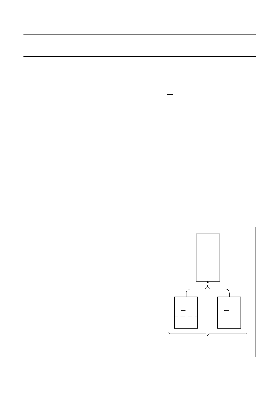
9.2
Internal Data Memory
The internal data memory is divided into three physically
separated parts: 256 byte of RAM, 256 byte of AUX-RAM,
and a 128 byte special function area (SFR). These parts
can be addressed as follows (see Table 3 and Fig.11):
∑
RAM 0 to 127 can be addressed directly and indirectly
as in the 80C51. Address pointers are R0 and R1 of the
selected register bank.
∑
RAM 128 to 255 can only be addressed indirectly.
Address pointers are R0 and R1 of the selected register
bank.
∑
AUX-RAM 0 to 255 is indirectly addressable as the
external data memory locations 0 to 255 with the MOVX
instructions. Address pointers are R0 and R1 of the
selected register bank and DPTR. When executing from
internal program memory, an access to AUX-RAM 0 to
255 will not affect the ports P0, P2, P3.6 and P3.7.
∑
the SFRs can only be addressed directly in the address
range from 128 to 255.
An access to external data memory locations higher than
255 will be performed with the MOVX DPTR instructions in
the same way as in the 80C51 structure, i.e. with P0 and
P2 as data/address bus and P3.6 and P3.7 as write and
read timing signals (see Figures 7, 8, 9 and 10). Note that
the external data memory cannot be accessed with R0 and
R1 as address pointer.
Fig.11 shows the internal and external data memory
address space. Fig.12 shows the Special Function
Register (SFR) memory map. Four 8-bit register banks
occupy locations 0 through 31 in the lower RAM area. Only
one of these banks may be enabled at a time. The next 16
bytes, locations 32 through 47, contain 128 directly
addressable bit locations.
The stack can be located anywhere in the internal 256 byte
RAM. The stack depth is only limited by the available
internal RAM space of 256 bytes. All registers except the
Program Counter and the four 8-bit register banks reside
in the SFR address space.
Table 3
Internal data memory access
LOCATION
ADDRESSED
RAM 0 to 127
DIRECT and INDIRECT
RAM 128 to 255
INDIRECT only
AUX-RAM 0 to 255
INDIRECT only with MOVX
Special Function Register (SFR) 128 to 255
DIRECT only
1997 Dec 15
15
Philips Semiconductors
Product specification
8-bit microcontrollers
P83C524; P80C528; P83C528
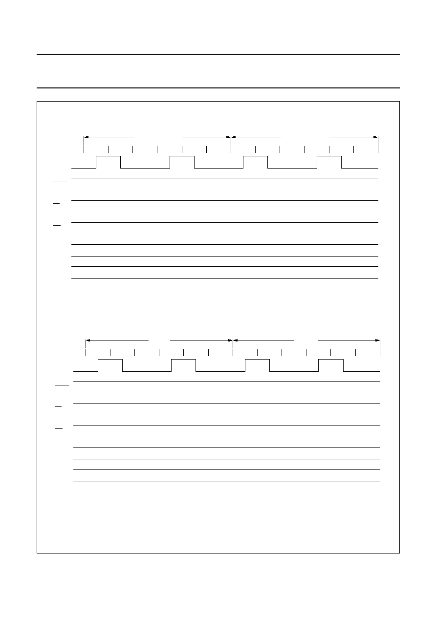
Fig.7 Internal program memory execution.
a. Without a MOVX.
b. With a MOVX to the AUX-RAM (read and write).
handbook, full pagewidth
MBC458
S1
S2
S3
S4
S5
S6
S1
S2
S3
S4
S5
S6
cycle 1
cycle 2
ALE
PSEN
RD
WR
P0
P0 OUT
P2
P2 OUT
handbook, full pagewidth
MBC457
S1
S2
S3
S4
S5
S6
S1
S2
S3
S4
S5
S6
one machine cycle
ALE
PSEN
RD
WR
P0
P0 OUT
P2
P2 OUT
one machine cycle

1997 Dec 15
16
Philips Semiconductors
Product specification
8-bit microcontrollers
P83C524; P80C528; P83C528
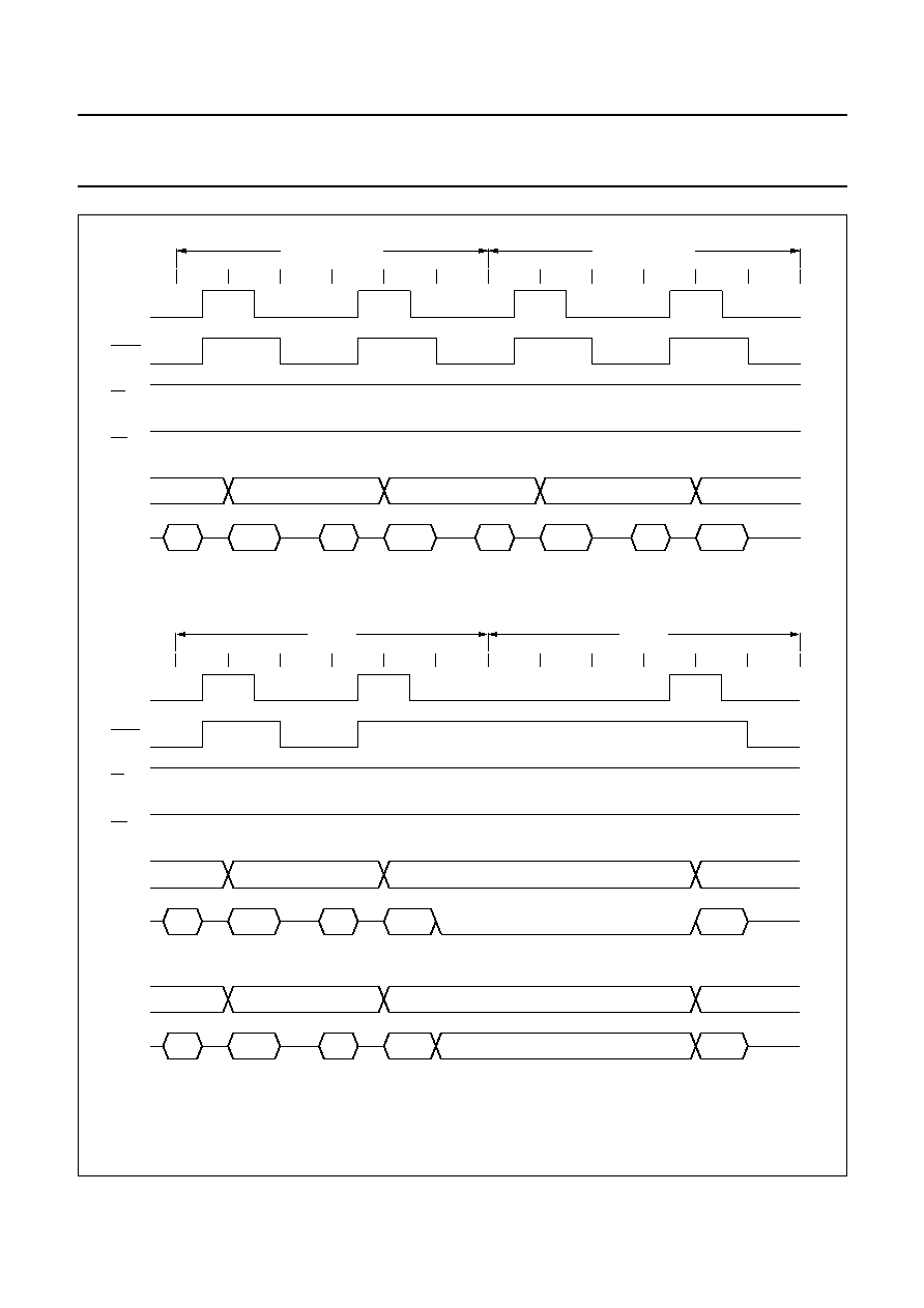
Fig.8 Internal program memory execution (continued).
handbook, full pagewidth
MBC460
S1
S2
S3
S4
S5
S6
S1
S2
S3
S4
S5
S6
cycle 1
cycle 2
ALE
PSEN
RD
WR
P0
DPL
OUT
P0 OUT
P2
P2 OUT
DPH OUT
P2 OUT
DATA OUT
a. With a MOVX to the External Data Memory (read).
b. With a MOVX to the External Data Memory (write).
handbook, full pagewidth
MBC459
S1
S2
S3
S4
S5
S6
S1
S2
S3
S4
S5
S6
cycle 1
cycle 2
ALE
PSEN
RD
WR
P0
DATA
IN
DPL
OUT
P0 OUT
P2
P2 OUT
DPH OUT
P2 OUT
1997 Dec 15
17
Philips Semiconductors
Product specification
8-bit microcontrollers
P83C524; P80C528; P83C528
Fig.9 External program memory execution.
a. Without a MOVX.
b. With a MOVX to the AUX-RAM (read and write).
handbook, full pagewidth
MBC462
S1
S2
S3
S4
S5
S6
S1
S2
S3
S4
S5
S6
ALE
PSEN
RD
WR
P0
P2
PCH OUT
cycle 1
cycle 2
PCH OUT
ADDRH OUT
PCH OUT
PCL
OUT
INST
IN
ADDRL
OUT
INST
IN
PCL
OUT
P0
P2
PCH OUT
PCH OUT
ADDRH OUT
PCH OUT
PCL
OUT
INST
IN
ADDRL
OUT
INST
IN
PCL
OUT
DATA OUT
(read)
(write)
handbook, full pagewidth
MBC461
S1
S2
S3
S4
S5
S6
S1
S2
S3
S4
S5
S6
ALE
PSEN
RD
WR
P0
P2
PCH OUT
one machine cycle
one machine cycle
PCH OUT
PCH OUT
PCH OUT
PCH OUT
INST
IN
PCL
OUT
INST
IN
PCL
OUT
INST
IN
PCL
OUT
INST
IN
PCL
OUT

1997 Dec 15
18
Philips Semiconductors
Product specification
8-bit microcontrollers
P83C524; P80C528; P83C528
Fig.10 External program memory execution (continued).
a. With a MOVX to the External Data Memory (read).
b. With a MOVX to the External Data Memory (write).
handbook, full pagewidth
S1
S2
S3
S4
S5
S6
S1
S2
S3
S4
S5
S6
ALE
PSEN
RD
WR
P0
P2
PCH OUT
cycle 1
cycle 2
PCH OUT
DPH OUT
PCH OUT
PCL
OUT
INST
IN
DPL
OUT
INST
IN
PCL
OUT
MBC464
DATA OUT
handbook, full pagewidth
S1
S2
S3
S4
S5
S6
S1
S2
S3
S4
S5
S6
ALE
PSEN
RD
WR
P0
P2
PCH OUT
cycle 1
cycle 2
PCH OUT
DPH OUT
PCH OUT
PCL
OUT
INST
IN
DPL
OUT
INST
IN
PCL
OUT
MBC463
DATA
IN

1997 Dec 15
19
Philips Semiconductors
Product specification
8-bit microcontrollers
P83C524; P80C528; P83C528
Fig.11 Internal and external data memory address space.
handbook, full pagewidth
MBC466 - 1
FFFF
0100
FF
00
00
7F
80
FF
FF
80
SHARED
ADDRESS LOCATION
DATA MEMORY
register
indirect
addressing
direct byte
addressing
SPECIAL
FUNCTION
REGISTERS
EXTERNAL
DATA
MEMORY
AUX - RAM
256 BYTES
LOWER
128 BYTES
INTERNAL
RAM
UPPER
128 BYTES
INTERNAL
RAM

1997 Dec 15
20
Philips Semiconductors
Product specification
8-bit microcontrollers
P83C524; P80C528; P83C528
Fig.12 Special Function Register (SFR) memory map.
handbook, full pagewidth
MBC465 - 1
F7
F6
F5
F4
F3
F2
F1
F0
F0H
B
E0H
ACC
E7
E6
E5
E4
E3
E2
E1
E0
DAH
S1INT
D9H
S1BIT
SDI/
SDO
DF
SCI/
SCO
DE
CLH
DO
BB
DC
RBF
DB
WBF
DA
STR
D9
ENS
D8
D8H
S1SCS
FFH
T3
CY
D7
AC
D6
FO
D5
RSI
D4
RSO
D3
OV
D2
FI
D1
P
D0
D0H
PSW
CDH
TH2
CCH
TL2
CBH
RCAP2H
CAH
RCAP2L
TF2
CF
EXF2
CE
RCLK
CD
TCLK
CC
EXEN2
CB
TR2
CA
C8H
T2CON
- - -
BF
PS1
BE
PT2
BD
PS
BC
PT1
BB
PX1
BA
PT0
B9
PX0
B8
B8H
IP
B0H
P3
EA
AF
ES1
AE
ET2
AD
ES
AC
ET1
AB
EX1
AA
ET0
A9
EX0
A8
A8H
IE
B7
B6
B5
B4
B3
B2
B1
B0
CP/RL2
C8
C/T2
C9
A0H
P2
A7
A6
A5
A4
A3
A2
A1
A0
A5H
WDCON
99H
SBUF
SM0
9F
SM1
9E
SM2
9D
REN
9C
TB8
9B
RB8
9A
TI
99
RI
98
98H
SCON
90H
P1
97
96
95
94
93
92
91
90
8DH
TH1
TF1
8F
TR1
8E
TF0
8D
TR0
8C
IE1
8B
IT1
8A
IE0
89
IT0
88
88H
TCON
8CH
TH0
8BH
TL1
8AH
TL0
89H
TMOD
87H
PCON
80H
P0
87
86
85
84
83
82
81
80
81H
82H
83H
DPH
DPL
SP
REGISTER
MNEMONIC
BIT MNEMONIC /
BIT ADDRESS (HEX)
DIRECT BYTE
ADDRESS (HEX)

1997 Dec 15
21
Philips Semiconductors
Product specification
8-bit microcontrollers
P83C524; P80C528; P83C528
9.3
Addressing
The P83C528 has five modes for addressing:
∑
Register
∑
Direct
∑
Register-Indirect
∑
Immediate
∑
Base-Register plus Index-Register-Indirect.
The first three methods can be used for addressing
destination operands. Most instructions have a
'destination/source' field that specifies the data type,
addressing methods and operands involved. For
operations other than MOVs, the destination operand is
also a source operand.
Access to memory addresses is as follows:
∑
Register in one of the four 8-bit register banks through
Register, Direct or Register-Indirect addressing.
∑
512 bytes of internal RAM through Direct or
Register-Indirect addressing. Bytes 0-127 of internal
RAM may be addressed directly/indirectly. Bytes
128-255 of internal RAM share their address location
with the SFRs and so may only be addressed indirectly
as data RAM. Bytes 0-255 of AUX-RAM can only be
addressed indirectly via MOVX.
∑
SFR through Direct addressing at address locations
128-255.
∑
External data memory through Register-Indirect
addressing.
∑
Program memory look-up tables through Base-Register
plus Index-Register-Indirect addressing.
1997 Dec 15
22
Philips Semiconductors
Product specification
8-bit microcontrollers
P83C524; P80C528; P83C528
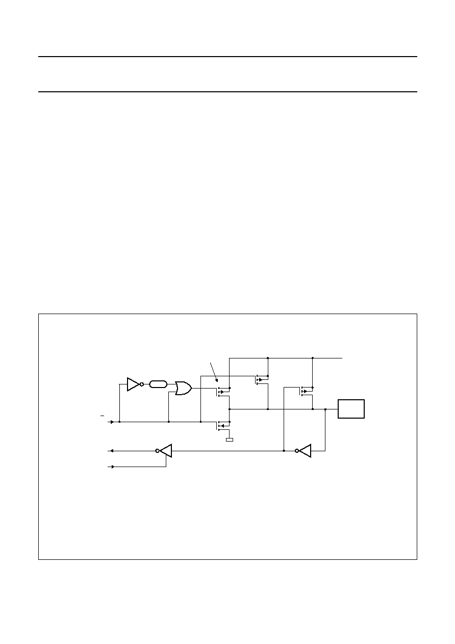
10 I/O FACILITIES
The P83C528 has four 8-bit ports. Ports 0-3 are the same
as in the 80C51, with the exception of the additional
function of Port 1. Port lines P1.0 and P1.1 may be used
as inputs for Timer 2, P1.1 may also be used as an
additional (third) external interrupt request input. Port lines
P1.6 and P1.7 may be selected as the SCL and SDA lines
of Serial Port SIO1 (I
2
C). Because the I
2
C-bus may be
active while the device is disconnected from V
DD
, these
pins are provided with open drain drivers. Pins P1.6 and
P1.7 do not have pull-up devices when used as ports.
Ports 0, 1, 2, and 3 perform the following alternative
functions:
∑
Port 0: provides the multiplexed low-order address and
data bus used for expanding the P83C528 with standard
memories and peripherals.
∑
Port 1: pins can be configured individually to provide:
external interrupt request input (external interrupt 2);
external inputs for Timer/counter 2; SCL and SDA for
the I
2
C interface.
∑
Port 2: provides the high-order address bus when
expanding the P83C528 with external program memory
and/or external data memory.
∑
Port 3: pins can be configured individually to provide:
external interrupt request inputs (external interrupt 0/1);
external inputs for Timer/counter 0 and
Timer/counter 1; Serial Port receiver input and
transmitter output control-signals to read and write
external data memory.
Bits which are not used for the alternative functions may be
used as normal bidirectional I/O pins. The generation or
use of a Port 1 or Port 3 pin as an alternative function is
carried out automatically by the P83C528 provided the
associated SFR bit is HIGH. Otherwise the port pin is held
at a logical LOW level.
Fig.13 I/O buffers in the P83C528 (Ports 1, 2 and 3 except P1.6 and P1.7).
handbook, full pagewidth
MLA513
p1
p2
p3
input data
read port pin
2 oscillator
periods
n
strong pull-up
I/O PIN
PORT
+5 V
I1
Q
from port latch
INPUT
BUFFER

1997 Dec 15
23
Philips Semiconductors
Product specification
8-bit microcontrollers
P83C524; P80C528; P83C528
11 TIMERS/COUNTERS
The P83C528 contains three 16-bit timer/counters, Timer
0, Timer 1 and Timer 2, and one 8-bit timer, the Watchdog
Timer T3. Timer 0, Timer 1 and Timer 2 may be
programmed to carry out the following functions:
∑
measure time intervals and pulse durations
∑
count events
∑
generate interrupt requests.
11.1
Timer 0 and Timer 1
Timers 0 and 1 each have a control bit in TMOD SFR that
selects the timer or counter function of the corresponding
timer. In the timer function, the register is incremented
every machine cycle. Thus, one can think of it as counting
machine cycles. Since a machine cycle consists of 12
oscillator periods, the count rate is
1
/
12
of the oscillator
frequency.
In the counter function, the register is incremented in
response to a HIGH-to-LOW transition at the
corresponding external input pin, T0 or T1. In this function,
the external input is sampled during S5P2 of every
machine cycle. When the samples show a HIGH in one
cycle and a LOW in the next cycle, the counter is
incremented. Thus, it takes two machine cycles (24
oscillator periods) to recognize a HIGH-to-LOW transition.
There are no restrictions on the duty cycle of the external
input signal, but to ensure that a given level is sampled at
least once before it changes, it should be held for at least
one full machine cycle.
Timer 0 and Timer 1 can be programmed independently to
operate in one of four modes:
Mode 0 8-bit timer/counter with divide-by-32 prescaler
Mode 1 16-bit timer/counter
Mode 2 8-bit timer/counter with automatic reload
Mode 3 Timer 0: one 8-bit timer/counter and one 8-bit
timer. Timer 1: stopped.
When Timer 0 is in Mode 3, Timer 1 can be programmed
to operate in Modes 0, 1 or 2 but cannot set an interrupt
request flag and generate an interrupt. However, the
overflow from Timer 1 can be used to pulse the Serial Port
transmission-rate generator. With a 16 MHz crystal, the
counting frequency of these timer/counters is as follows:
∑
in the timer function, the timer is incremented at a
frequency of 1.33 MHz (oscillator frequency divided by
12).
∑
in the counter function, the frequency handling range for
external inputs is 0 Hz to 0.66 MHz.
Both internal and external inputs can be gated to the timer
by a second external source for directly measuring pulse
duration.
The timers are started and stopped under software control.
Each one sets its interrupt request flag when it overflows
from all logic 1's to all logic 0's (respectively, the automatic
reload value), with the exception of Mode 3 as previously
described.

1997 Dec 15
24
Philips Semiconductors
Product specification
8-bit microcontrollers
P83C524; P80C528; P83C528
11.1.1
T
IMER
/C
OUNTER
M
ODE
C
ONTROL REGISTER
(TMOD)
Table 4
Timer/Counter Mode Control register (address 89H)
Table 5
Description of the TMOD bits
Table 6
TMOD M1 and M0 operating modes
7
6
5
4
3
2
1
0
TIMER 1
TIMER 0
GATE
C/T
M1
M0
GATE
C/T
M1
M0
BIT
SYMBOL
FUNCTION
TIMER 1
7
GATE
Timer 1 gating control: when set, Timer/counter '1' is enabled only while 'INT1' pin is
HIGH and 'TR1' control bit is set. When cleared, Timer/counter '1' is enabled whenever
'TR1' control bit is set.
6
C/T
Timer or counter selector: cleared for timer operation (input from internal system
clock). Set for counter operation (input from 'T1' input pin).
5
M1
operating mode: see Table 6.
4
M0
operating mode: see Table 6.
TIMER 0
3
GATE
Timer 0 gating control: when set, Timer/counter '0' is enabled only while 'INT0' pin is
HIGH and 'TR0' control bit is set. When cleared, Timer/counter '0' is enabled whenever
'TR0' control bit is set.
2
C/T
Timer or counter selector: cleared for timer operation (input from internal system
clock). Set for counter operation (input from 'T0' input pin).
1
M1
operating mode: see Table 6.
0
M0
operating mode: see Table 6.
M1
M0
FUNCTION
0
0
8-bit timer/counter: 'THx' with 5-bit prescaler.
0
1
16-bit timer/counter: 'THx' and 'TLx' are cascaded, there is no prescaler.
1
0
8-bit autoload timer/counter: 'THx' holds a value which is to be reloaded into 'TLx'
each time it overflows.
1
1
Timer 0: TL0 is an 8-bit timer/counter controlled by the standard Timer 0 control bits.
TH0 is an 8-bit timer controlled by Timer 1 control bits.
1
1
Timer 1: Timer/counter 1 stopped.
1997 Dec 15
25
Philips Semiconductors
Product specification
8-bit microcontrollers
P83C524; P80C528; P83C528
11.1.2
T
IMER
/C
OUNTER
C
ONTROL
R
EGISTER
(TCON)
Table 7
Timer/Counter Control register (address 88H)
Table 8
Description of the TCON bits
7
6
5
4
3
2
1
0
TF1
TR1
TF0
TR0
IE1
IT1
IE0
IT0
BIT
SYMBOL
FUNCTION
7
TF1
Timer 1 overflow flag: set by hardware on timer/counter overflow. Cleared when
interrupt is processed.
6
TR1
Timer 1 run control bit: set/cleared by software to turn timer/counter ON/OFF.
5
TF0
Timer 0 overflow flag: set by hardware on timer/counter overflow. Cleared when
interrupt is processed.
4
TR0
Timer 0 run control bit: set/cleared by software to turn timer/counter ON/OFF.
3
IE1
Interrupt 1 edge flag: set by hardware when external interrupt is detected. Cleared
when interrupt is processed.
2
IT1
Interrupt 1 type control bit: set/cleared by software to specify falling edge/LOW level
triggered external interrupt.
1
IE0
Interrupt 0 edge flag: set by hardware when external interrupt is detected. Cleared
when interrupt is processed.
0
IT0
Interrupt 0 type control bit: set/cleared by software to specify falling edge/LOW level
triggered external interrupt.

1997 Dec 15
26
Philips Semiconductors
Product specification
8-bit microcontrollers
P83C524; P80C528; P83C528
11.2
Timer 2
Timer 2 is functionally similar to the Timer 2 of the 8052AH. Timer 2 is a 16-bit timer/counter which is formed by two
SFRs, TL2 and TH2. Another pair of SFRs, RCAP2L and RCAP2H, form a 16-bit capture register or a 16-bit reload
register. Like Timer 0 and 1, Timer 2 can operate either as timer or as event counter. This is selected by bit C/T2 in the
T2CON SFR. The timer has three operating modes: 'capture', 'autoload' and 'baud rate generator', which are selected
by bits in the T2CON SFR (see Table 9).
Table 9
Timer 2 operating modes
11.2.1
T
IMER
2 C
ONTROL
R
EGISTER
(T2CON)
Table 10 Timer 2 Control register (address C8H)
Table 11 Description of the T2CON bits
RCLK + TCLK
CP/RL2
TR2
MODE
0
0
1
16-bit automatic reload
0
1
1
16-bit capture
1
X
1
baud rate generator
X
X
0
OFF
7
6
5
4
3
2
1
0
TF2
EXF2
RCLK
TCLK
EXEN2
TR2
C/T2
CP/RL2
MNEMONIC
POSITION
FUNCTION
TF2
T2CON.7
Timer 2 overflow flag: set by a Timer 2 overflow and must be cleared by software. TF2
will not be set when either RCLK = 1 or TCLK = 1. When Timer 2 interrupt is enabled,
TF2 = 1 (see EXF2).
EXF2
T2CON.6
Timer 2 external flag: set when either a capture or reload is caused by a negative
transition on T2EX and EXEN2 = 1. When Timer 2 interrupt is enabled, EXF2 = 1 will
cause the CPU to vector to Timer 2 interrupt routine.
RCLK
T2CON.5
Receive clock flag: when set, causes the Serial Port to use Timer 2 overflow pulses for
its receive clock in Modes 1 and 3. RCLK = 0 causes Timer 1 overflows to be used for
the receive clock.
TCLK
T2CON.4
Transmit clock flag: when set, causes the Serial Port to use Timer 2 overflow pulses
for its transmit clock in Modes 1 and 3. TCLK = 0 causes Timer 1 overflows to be used
for the transmit clock.
EXEN2
T2CON.3
Timer 2 external enable flag: when set, allows a capture or reload to occur as a result
of a negative transition on T2EX if Timer 2 is not being used to clock the Serial Port.
EXEN2 = 0 causes Timer 2 to ignore events at T2EX.
TR2
T2CON.2
Start/stop control: a logic 1 starts Timer 2. A logic 0 stops Timer 2.
C/T2
T2CON.1
Timer/counter select: 0 = internal timer (OSC/12). 1 = external event counter (falling
edge triggered).
CP/RL2
T2CON.0
Capture/reload flag: when set, capture will occur on negative transitions at T2EX if
EXEN2 = 1. When cleared, reloads will occur upon either Timer 2 overflows or negative
transitions at T2EX if EXEN2 = 1. When either RCLK = 1 or TCLK = 1, this bit is ignored
and the timer is forced to reload upon overflow.

1997 Dec 15
27
Philips Semiconductors
Product specification
8-bit microcontrollers
P83C524; P80C528; P83C528
11.2.2
C
APTURE
M
ODE
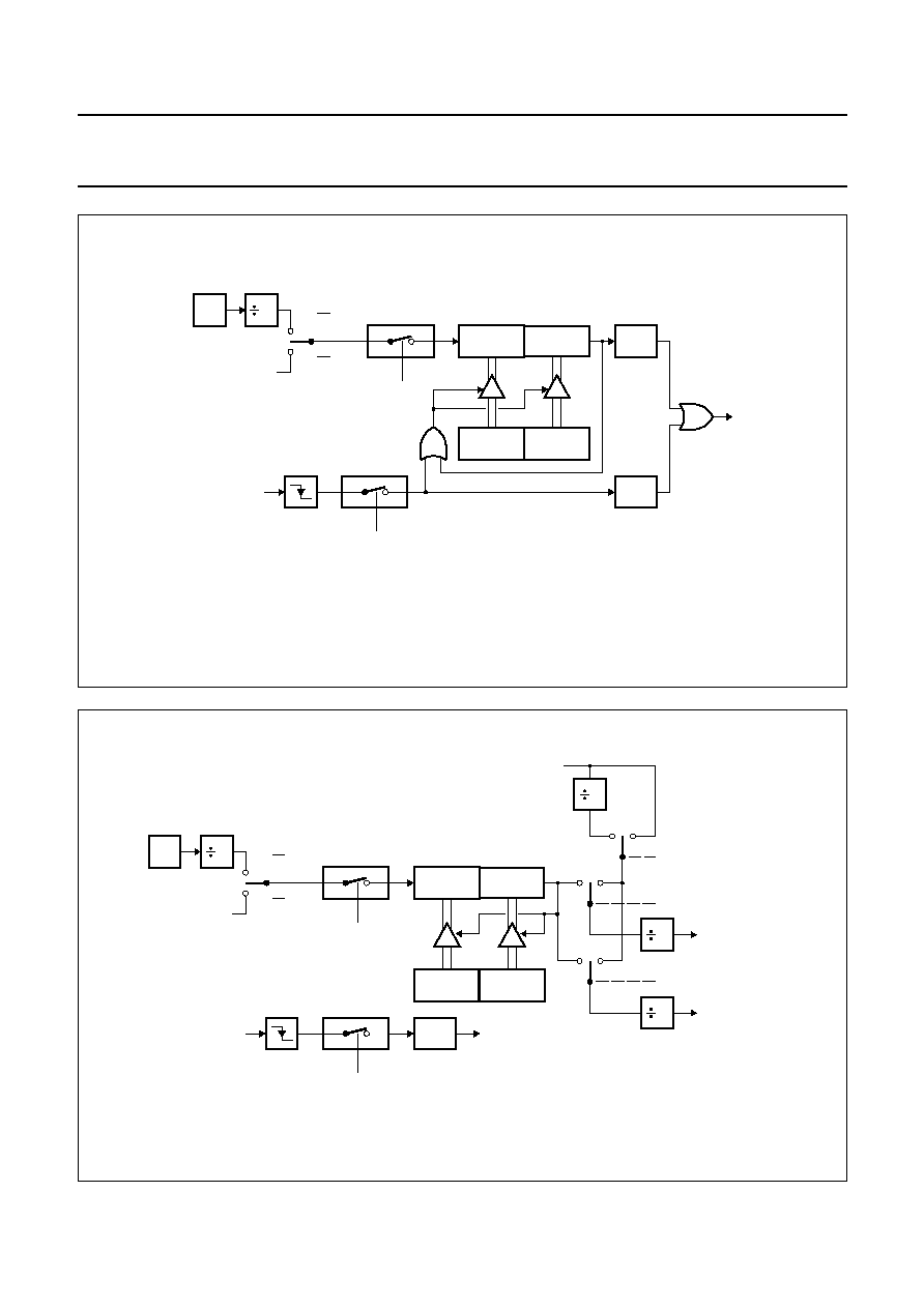
In the capture mode (see Fig.14) there are two options
which are selected by bit EXEN2 in T2CON. If EXEN2 = 0,
then Timer 2 is a 16-bit timer/counter which on overflow
sets bit TF2 (Timer 2 overflow bit). TF2 can be used to
generate an interrupt. If EXEN2 = 1, Timer 2 operates as
above, with the added feature that a HIGH-to-LOW
transition at the external input T2EX causes the current
value in Timer 2 registers (TL2 and TH2) to be captured
into registers RCAP2L and RCAP2H, respectively. The
HIGH-to-LOW transition of T2EX also causes bit EXF2 in
T2CON to be set. EXF2 can be used to generate an
interrupt.
11.2.3
A
UTOMATIC
R
ELOAD
M
ODE
In the automatic reload mode (see Fig.15)there are two
options which are selected by bit EXEN2 in T2CON. If
EXEN2 = 0, then a Timer 2 overflow sets TF2 and causes
the Timer 2 registers to be reloaded with the 16-bit value
in registers RCAP2L and RCAP2H, which are preset by
software.
If EXEN2 = 1, Timer 2 operates as above, with the added
feature that a HIGH-to-LOW transition at the external input
T2EX triggers the 16-bit reload and sets EXF2.
11.2.4
B
AUD
R
ATE
G
ENERATOR
M
ODE
The baud rate generator mode (see Fig.16) is selected by
RCLK = 1 and/or TCLK = 1 in T2CON. Overflows of either
Timer 2 or Timer 1 can be used independently for
generating baud rates for transmit and receive. The baud
rate generation by Timer 1 and/or Timer 2 is used for the
Serial Port in Mode 1 and Mode 3. The baud rate
generation mode is similar to the automatic reload mode,
in that a rollover in TH2 causes the Timer 2 registers to be
reloaded with the 16-bit value in registers RCAP2L and
RCAP2H, which are preset by software. The baud rate for
the Serial Port in Modes 1 and 3 are determined by
Timer 2's overflow rate as follows:
Timer 2 can be configured for either 'timer' or 'counter'
operation. In timer operation a prescaler divides the
oscillator frequency by 2 (by 12 in the previous modes) and
the baud rate is given by the formula:
In this mode an overflow of Timer 2 does not set TF2. If
EXEN2 = 1, a HIGH-to-LOW transition at pin T2EX sets
EXF2 and can be used to generate an interrupt.
Baud Rate
Timer 2 overflow rate
16
--------------------------------------------------------
=
Baud Rate
oscillator frequency
32
65536
RCAP2H RCAP2L
(
,
)
]
≠
[
◊
-------------------------------------------------------------------------------------------------------
=
Fig.14 Timer 2 in capture mode.
handbook, full pagewidth
MBC468 - 1
TL2
(8 BITS)
TR2
control
TH2
(8 BITS)
RCAP2L
RCAP2H
EXF2
TF2
timer 2
interrupt
EXEN2
control
C/T2 = 1
T2 PIN
12
OSC
transition
detector
T2EX PIN
C/T2 = 0
1997 Dec 15
28
Philips Semiconductors
Product specification
8-bit microcontrollers
P83C524; P80C528; P83C528
Fig.15 Timer 2 in automatic reload mode.
handbook, full pagewidth
MBC469 - 1
TL2
(8 BITS)
TR2
control
TH2
(8 BITS)
RCAP2L
RCAP2H
EXF2
TF2
timer 2
interrupt
EXEN2
control
C/T2 = 0
C/T2 = 1
T2 PIN
12
OSC
transition
detector
T2EX PIN
reload
Fig.16 Timer 2 in baud rate generator mode.
handbook, full pagewidth
MBC470 - 1
TL2
(8 BITS)
TR2
control
TH2
(8 BITS)
RCAP2L
RCAP2H
EXF2
EXEN2
control
C/T2 = 0
C/T2 = 1
T2 PIN
2
OSC
transition
detector
T2EX PIN
"TIMER 2"
interrupt
(additional external
interrupt)
(note: divided by 2
not by 12)
16
RCLK
16
TCLK
RX CLOCK
TX CLOCK
SMOD
1
0
1
0
1
0
2
TIMER 1
overflow

1997 Dec 15
29
Philips Semiconductors
Product specification
8-bit microcontrollers
P83C524; P80C528; P83C528
11.3
Watchdog Timer T3
The Watchdog Timer (WDT) see Fig.17, consists of an
11-bit prescaler and an 8-bit timer formed by SFR T3. The
prescaler is incremented by an on-chip oscillator with a
fixed frequency of 1 MHz. The maximum tolerance on this
frequency is
-
50% and +100%. The 8-bit timer increments
every 2048 cycles of the on-chip oscillator. When a timer
overflow occurs, the microcontroller is reset and a
reset-output-pulse of 16 x 2048 cycles of the on-chip
oscillator is generated at pin RST. The internal RESET
signal is not inhibited when the external RST pin is kept
LOW by e.g. an external reset circuit. The RESET signal
drives Ports 1, 2 and 3 outputs into the High state and Port
0 into high impedance, no matter if the XTAL-clock is
running or not.
The WDT is controlled by WDCON SFR with the direct
address location A5H. WDCON can be read and written by
software. A value of A5H in WDCON halts the on-chip
oscillator and clears both the prescaler and Timer T3. After
RESET, WDCON contains A5H. Every value other than
A5H in WDCON enables the WDT. When the WDT is
enabled it runs independent of the XTAL-clock.
Timer T3 can be read on the fly. Timer T3 can be written
only if WDCON has previously been loaded with 5AH,
otherwise T3 and the prescaler are not affected. A
successful write operation to T3 also clears the prescaler
and clears WDCON. During a read or write operation
addressing T3, the output of the on-chip oscillator is
inhibited to prevent timing problems due to asynchronous
increments of T3. To prevent an overflow of the WDT, the
user program has to reload T3 within periods that are
shorter than the programmed Watchdog time interval. This
time interval is determined by the 8-bit reload value that is
written into register T3.
The advantages of this implementation are:
∑
Only an internal reset connection to the microcontroller
core
∑
The Power-down mode and the Watchdog (WDT)
function can be used concurrently
∑
The WDT also monitors the XTAL oscillator. In case of a
failure the port outputs are forced to a defined High state
∑
Interference will not disable the WDT because it is
unlikely that it will force WDCON to A5H
∑
Tolerances of the on-chip oscillator can be adjusted by
testing the T3 value and adapting the reload value
∑
The WDT can be enabled and disabled under control of
the user software. This gives the possibility to use both
the Watchdog function and the Power-down function
∑
The direct address A5H of WDCON and its disable value
A5H will not unintentionally be present at a random
location in the field of program code, except for
immediate data, because the opcode A5H is not used in
the instruction set.
Watchdog time interval
256
T3
)
(
≠
[
]
2048
◊
on-chip oscillator frequency
-------------------------------------------------------------------------
=
Fig.17 Watchdog Timer T3.
handbook, full pagewidth
MBC471 - 1
8 - BIT TIMER
T3
11 - BIT
PRESCALER
WDCON
clear
input
A5H
5AH
clear
ON - CHIP -
OSCILLATOR
halt
write
read
clear
WR - T3
RD - T3
over-flow
VDD
VSS
internal
RESET
RST
this signal is active if WDCON
contains this hex value
IBS
R RST
(1)
(1)
(1)

1997 Dec 15
30
Philips Semiconductors
Product specification
8-bit microcontrollers
P83C524; P80C528; P83C528
12 SERIAL PORT (UART)
The Serial Port is functionally similar to the implementation
in the 8052AH, with the possibility of two different baud
rates for receive and transmit with Timer 1 and Timer 2 as
baud rate generators. It is full duplex, meaning it can
receive and transmit simultaneously. It is also
receive-buffered, meaning it can commence reception of a
second byte before a previously received byte has been
read from the receive register. However, if the first byte still
has not been read by the time the reception of the second
byte is complete, one of the bytes will be lost. The Serial
Port receive and transmit registers are both accessed as
SBUF SFR. Writing to SBUF loads the transmit register,
and reading SBUF accesses the physically separate
receive register. The Serial Port can operate in one of four
modes:
Mode 0 serial data enters and exits through RXD. TXD
outputs the shift clock. 8 bits are
transmitted/received: 8 data bits (LSB first). The
baud rate is fixed at 1/12 the oscillator frequency.
Mode 1 10 bits are transmitted (through TXD) or received
(through RXD): a start bit (0), 8 data bits (LSB
first), and a stop bit (1). On receive, the stop bit
goes into RB8 in SCON SFR. The baud rate is
variable.
Mode 2 11 bits are transmitted (through TXD) or received
(through RXD): a start bit (0), 8 data bits (LSB
first), a programmable 9th data bit, and a stop bit
(1). On transmit, the 9th data bit (TB8 in SCON)
can be assigned the value of 0 or 1. For example,
the parity bit (P, in the PSW) could be moved into
TB8. On receive, the 9th data bit goes into RB8 in
SCON, while the stop bit is ignored. The baud
rate is programmable to either 1/32 or 1/64 the
oscillator frequency.
Mode 3 11 bits are transmitted (through TXD) or received
(through RXD): a start bit (0), 8 data bits (LSB
first), a programmable 9th data bit, and a stop bit
(1). In fact, Mode 3 is the same as Mode 2 in all
respects except the baud rate. The baud rate in
Mode 3 is variable.
In all four modes, transmission is initiated by any
instruction that uses SBUF as a destination register. In
Mode 0, reception is initiated by the condition RI = 0 and
REN = 1. Reception is initiated by incoming start bit if
REN = 1 in the other modes.

1997 Dec 15
31
Philips Semiconductors
Product specification
8-bit microcontrollers
P83C524; P80C528; P83C528
12.1
Serial Port Control Register (SCON)
Table 12 Serial Port Control register (address 98H)
Table 13 Description of the SCON bits
12.2
SM0 and SM1 operating modes (SCON)
SCON bits SM0 and SM1 can operate in the following modes (see Table 14):
Table 14 SM0 and SM1 operating modes
7
6
5
4
3
2
1
0
SM0
SM1
SM2
REN
TB8
RB8
TI
RI
BIT
SYMBOL
FUNCTION
7
SM0
see Table 14.
6
SM1
see Table 14.
5
SM2
Enables the multiprocessor communication feature in Modes 2 and 3. In these
modes, if SM2 is set to 1 then RI will not be activated if the received 9th data bit (RB8) is
0. In Mode 1, if SM2 = 1, then RI will not be activated if a valid stop bit is not received. In
Mode 0, SM2 should be 0.
4
REN
Enables serial reception. Set and cleared by software as required.
3
TB8
9th data bit that will be transmitted in Modes 2 and 3. Set and cleared by software
as required.
2
RB8
In Modes 2 and 3, RB8 is the 9th data bit that is received. In Mode 1, if SM2 = 0,
RB8 is the stop bit that is received. In Mode 0, RB8 is not used.
1
TI
Transmit interrupt flag. It is set by hardware at the end of the 8th bit time in Mode 0, or
at the beginning of the stop bit in the other modes. TI must be cleared by software.
0
RI
Receive interrupt flag. It is set by hardware at the end of the 8th bit time in Mode 0, or
halfway through the stop bit time in the other modes (except: see SM2). RI must be
cleared by software.
MODE
SM0
SM1
DESCRIPTION
BAUD RATE
0
0
0
shift register
1
/
12
f
OSC
1
0
1
8-bit UART
variable
2
1
0
9-bit UART
1
/
32
f
OSC
,
1
/
64
f
OSC
3
1
1
9-bit UART
variable

1997 Dec 15
32
Philips Semiconductors
Product specification
8-bit microcontrollers
P83C524; P80C528; P83C528
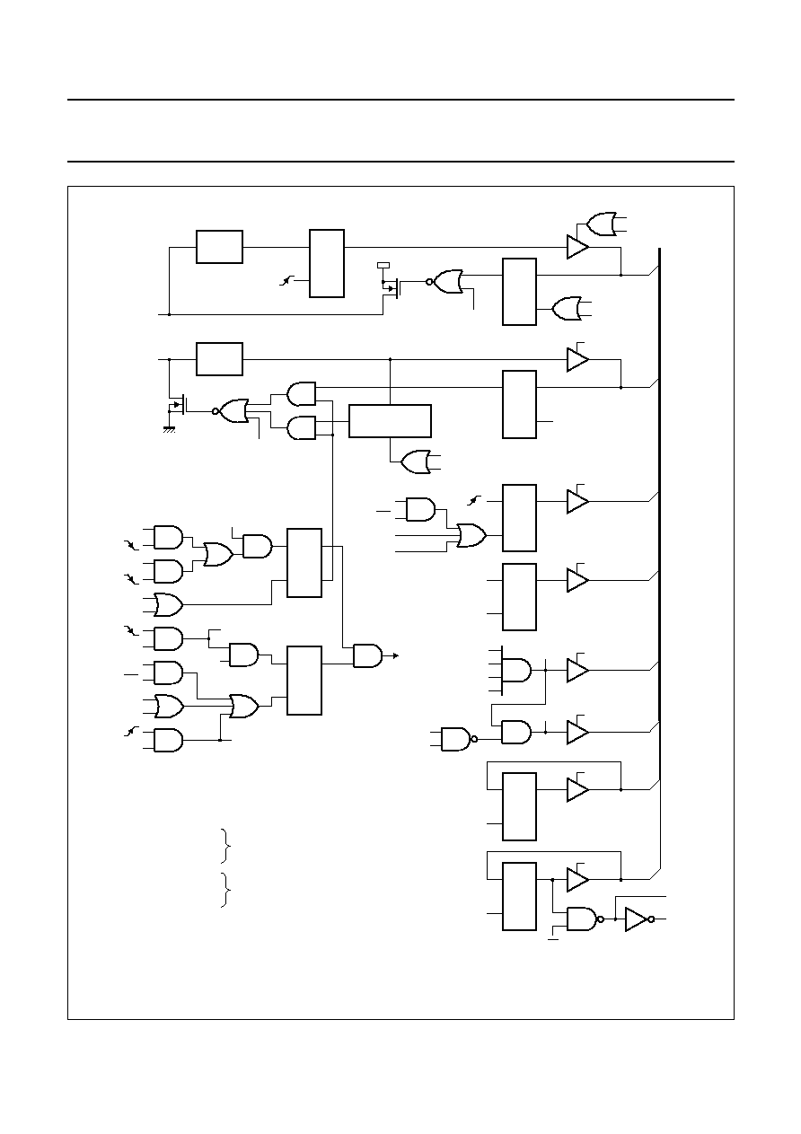
13 BIT-LEVEL I
2
C INTERFACE
This bit-level serial I/O interface supports the I
2
C-bus (see
Fig.18). P1.6/SCL and P1.7/SDA are the serial I/O pins.
These two pins meet the I
2
C specification concerning the
input levels and output drive capability. Consequently,
these pins have an open drain output configuration. All
four modes of the I
2
C-bus are supported:
∑
master transmitter
∑
master receiver
∑
slave transmitter
∑
slave receiver.
The advantages of the bit-level I
2
C hardware compared
with a full software I
2
C implementation are:
∑
the hardware can generate the SCL pulse
∑
testing a single bit (RBF respectively, WBF) is sufficient
as a check for error free transmission.
The bit-level I
2
C hardware operates on serial bit level and
performs the following functions:
∑
filtering the incoming serial data and clock signals
∑
recognizing the START condition
∑
generating a serial interrupt request SI after reception of
a START condition and the first falling edge of the serial
clock
∑
recognizing the STOP condition
∑
recognizing a serial clock pulse on the SCL line
∑
latching a serial bit on the SDA line (SDI)
∑
stretching the SCL LOW period of the serial clock to
suspend the transfer of the next serial data bit
∑
setting Read Bit Finished (RBF) when the SCL clock
pulse has finished and Write Bit Finished (WBF) if there
is no arbitration loss detected (i.e. SDA = 0 while
SDO = 1)
∑
setting a serial clock LOW-to-HIGH detected (CLH) flag
∑
setting a Bus Busy (BB) flag on a START condition and
clearing this flag on a STOP condition
∑
releasing the SCL line and clearing the CLH, RBF and
WBF flags to resume transfer of the next serial data bit
∑
generating an automatic clock if the single bit data
register S1BIT is used in master mode.
The following functions must be done in software:
∑
handling the I
2
C START interrupts
∑
converting serial to parallel data when receiving
∑
converting parallel to serial data when transmitting
∑
comparing the received slave address with its own
∑
interpreting the acknowledge information
∑
guarding the I
2
C status if RBF or WBF = 0.
additionally, if acting as master:
∑
generating START and STOP conditions
∑
handling bus arbitration
∑
generating serial clock pulses if S1BIT is not used.
Three SFRs control the bit-level I
2
C interface: S1INT,
S1BIT and S1SCS.
1997 Dec 15
33
Philips Semiconductors
Product specification
8-bit microcontrollers
P83C524; P80C528; P83C528
Fig.18 Bit level I
2
C interface block diagram.
handbook, full pagewidth
MBC484
RSCS
D
Q
ENS
C
WSCS
IB0
PD
DIS
EN
RSCS
D
Q
STR
C
WSCS
IB1
RSCS
IB2
RSCS
IB3
WBF
RBF
RSCS
S
Q
BB
R
IB4
SDIQN
SDOQ
CLHQ
STAQN
BBQ
FSCLN
START
STOP
RSCS
S
Q
CLH
R
IB5
FSCL
WSCS
IB5
RSBIT
WSBIT
RSCS
Q
D
SCO
C
IB6
AUTO - CLOCK
GENERATOR
RSBIT
WSBIT
WSCS
FSCL
S
Q
ST
R
STAQ
FSCL
STRQ
QN
EN
S
Q
STA
R
SI
to
interrupt
logic
SCL
FILTER
DIS
FSCL
SDA
FILTER
FSDA
Q
D
SDO
C
IB7
WSBIT
WSCS
RSBIT
RSCS
Q
D
SDI
C
DIS
QN
FSCL
EN
START
STOP
WSBIT
RSBIT
FSDA
FSCL
WSINT
FSDA
FSCL
IB7
WSBIT
RSBIT
P1.7 / SDA
P1.7 / SCL
IBX : internal data bus
RSCS : read
WSCS : write
RSBIT : read
WSBIT : write
WSINT : write S1INT
S1SCS
S1BIT (with auto-clock)

1997 Dec 15
34
Philips Semiconductors
Product specification
8-bit microcontrollers
P83C524; P80C528; P83C528
13.1
I
2
C Interrupt Register (S1INT)
Table 15 I
2
C Interrupt register (address DAH)
(1)
Note
1. SI bit: writing a logic 0 clears this bit, writing a logic 1 has no effect.
Table 16 Description of the S1INT bits
13.2
Single-bit Data Register with I
2
C Auto-clock (S1BIT)
Table 17 Single-bit Data register with I
2
C Auto-clock (address D9H)
(1)
Note
1. Access of the S1BIT SFR clears SI, CLH, RBF and WBF. It starts the auto-clock if SCO = 0.
Table 18 Description of the S1BIT bits
7
6
5
4
3
2
1
0
SI
X
X
X
X
X
X
X
BIT
SYMBOL
FUNCTION
7
SI
Serial Interrupt request (SI) flag: if a START condition occurs the SI flag in the S1INT
SFR is set on the falling edge of the filtered serial clock. If SI = 1 is detected during a
transfer this can be a 'spurious START' error condition. If no transfer is taking place the
SI = 1 is a START from an external master. Provided the bits EA and ES1 in IE SFR are
set, SI then generates an interrupt so that a slave address receive routine can be
started. SI can be cleared by accessing the S1BIT register or by writing '00' to S1INT.
Also after reception of a START condition, the LOW period of the clock pulse is
stretched, suspending the serial transfer to allow the software to take action. This clock
stretching is ended by a read or write access to S1BIT.
6 to 0
-
X = undefined during read, don't care during write.
7
6
5
4
3
2
1
0
READ
SDI
0
0
0
0
0
0
0
WRITE
SDO
X
X
X
X
X
X
X
BIT
SYMBOL
FUNCTION
7
SDO/SDI
Serial Data Output (SDO) and the filtered Serial Data Input (SDI). SDI data is latched
on the rising edge of the filtered serial clock. S1BIT.7 accesses the same memory
locations as S1SCS.7. S1BIT SFR is not bit-addressable.
6 to 0
-
X = don't care.

1997 Dec 15
35
Philips Semiconductors
Product specification
8-bit microcontrollers
P83C524; P80C528; P83C528
13.2.1
R
EADING OR
W
RITING THE
S1BIT SFR
Reading or writing the S1BIT SFR starts an I
2
C bit I/O
sequence: some flags are cleared (SI, CLH, RBF, WBF),
clock stretching is finished and the auto-clock is started.
An auto-clock pulse is 'OR-ed' with SCO and thus will be
output only if the SCO flag has been set to 0. SCO = 1
inhibits the auto-clock start, so a dummy read or write of
S1BIT SFR can be used to finish clock stretching and clear
SI, CLH, RBF and WBF if the auto-clock is not used.
The auto-clock is an active HIGH SCL pulse that starts 28
XTAL clock periods after the SDI read or SDO write via
S1BIT. The duration of the auto-clock pulse is 100 XTAL
clock periods. If the SCL line is kept LOW by any device
that wants to hold up the bus transfer, the auto-clock
counter waits after 20 XTAL clock periods so that the
auto-clock pulse length will be at least 80 XTAL clock
periods (5
µ
s at f
OSC
= 16 MHz).
Every bit I/O should be followed by a RBF or WBF bit test.
A bit transfer has been finished successfully if after reading
a bit the RBF flag is 1 or after writing a bit the WBF flag is
1. When after reading a bit the RBF flag is still 0, the bus
status just before the S1SCS status read can be
determined as follows:
∑
if CLH = 0 then a bus device is still stretching the clock
∑
if SCI = 1 while CLH = 1 then the SCL pulse is not
finished
∑
if BB = 0 there has been a STOP condition.
When after writing a bit the WBF flag is still 0 and none of
the 3 status conditions mentioned for RBF are found then
a 'bus arbitration lost' condition will be the cause. This can
be determined also from the states of the received bit and
the last transmitted bit: 'arbitration loss' if SDO = 1 and
SDI = 0.
13.3
Control and Status Register for the I
2
C-bus (S1SCS)
Table 19 Control and Status register for the I
2
C-bus (address D8H)
Notes
1. SDI and SCI bits: read-modify-write operations like 'SETB bit' or 'CLR bit' access SDO and SCO for reading and
writing.
2. CLH bit: writing a logic 0 clears this bit, writing a 1 has no effect.
3. RBF and WBF bits: writing a logic 0 to CLH also clears these bits.
4. X = don't care.
7
6
5
4
3
2
1
0
READ
SDI
(1)
SCI
(1)
CLH
(2)
BB
RBF
(3)
WBF
(4)
STR
ENS
WRITE
SDO
SCO
CLH
(2)
X
X
X
STR
ENS

1997 Dec 15
36
Philips Semiconductors
Product specification
8-bit microcontrollers
P83C524; P80C528; P83C528
Table 20 Description of the S1SCS bits
BIT
SYMBOL
FUNCTION
7
SDO/SDI
Serial Data Output and the filtered Serial Data Input. SDI data is latched on the rising
edge of the filtered serial clock. S1SCS.7 accesses the same memory locations as
S1BIT.7. Access of the data bit via S1SCS will not start an auto-clock pulse.
6
SCO/SCI
Serial Clock Output and the filtered Serial Clock Input. Serial clock output SCO is
'OR-ed' with the auto-clock. If SCO = 1 the auto-clock output is inhibited. The internal
clock stretching logic and external devices can pull the SCL line LOW. If the auto-clock
is not used, the SCL line has to be controlled by setting SCO = 1, waiting for CLH = 1
and setting SCO = 0 after the specified SCL HIGH time. (Because of the input filter,
CLH will be set at least 8 XTAL clock periods after the SCL LOW-to-HIGH transition.)
5
CLH
Serial Clock LOW-to-HIGH transition flag: set with a rising edge of the filtered serial
clock. CLH = 1 indicates that, since the last CLH reset, a new valid data bit has been
latched in SDI. CLH can be reset by writing a 0 to S1SCS.5 or by a read/write of S1BIT.
Clearing CLH also clears RBF and WBF.
4
BB
Bus Busy flag: indicating that there has been a START condition that was not yet
followed by a STOP condition.
3
RBF
Read Bit Finished flag: indicating a successful bit read.
RBF = 1 implies the following conditions:
CLH = 1: SCL had a rising edge
SCI = 0: the SCL pulse has finished
SI = 0: no START condition occurred
BB = 1: no STOP condition occurred
The RBF flag can be cleared by clearing the CLH flag.
2
WBF
Write Bit Finished flag: indicating a successful bit write. The same conditions as for
RBF are true and also no 'arbitration loss' condition occurred. Arbitration is lost if a
1 data bit in SDO was over-ruled on SDA by an external device. The WBF flag can be
cleared by clearing the CLH flag.
1
STR
STRetch control flag. STR = 1 enables stretching of all SCL LOW periods. This allows
the processor in I
2
C slave mode to react on a fast master. The STR flag remains set
until cleared by writing a 0 to S1SCS.1.
The STretch (ST) flag (not readable) pulls the serial clock LOW while ST = 1. The ST
flag is set on the falling edge of the filtered serial clock if STR = 1. It is also set after
reception of a START condition, regardless of the STR contents. ST is cleared with a
read or write of S1BIT.
0
ENS
ENable Serial I/O flag. ENS = 1 enables the START detection and clock stretching
logic. ENS = 0 can be used to switch off the I
2
C-bus hardware. Note that the SDO and
SCO control flags must be set to 1 before ENS is set to avoid pulling SCL or SDA lines
to 0.

1997 Dec 15
37
Philips Semiconductors
Product specification
8-bit microcontrollers
P83C524; P80C528; P83C528
14 INTERRUPT SYSTEM
The P83C528 contains the same interrupt structure as the
PCB80C51BH, but with a seven-source interrupt structure
with two priority levels (see Fig.19).
The External Interrupts INT0 and INT1 can each be either
level-activated or transition-activated, depending on bits
IT0 and IT1 in TCON SFR. The flags that actually generate
these interrupts are bits IE0 and IE1 in TCON. When an
external interrupt is generated, the corresponding request
flag is cleared by the hardware when the service routine is
vectored to, only if the interrupt was transition-activated. If
the interrupt was level-activated then the interrupt request
flag remains set until the external interrupt pin INTx goes
high.
The Timer 0 and Timer 1 Interrupts are generated by TF0
and TF1, which are set by a rollover in their respective
timer/counter register (except for Timer 0 in Mode 3 of the
serial interface). When a Timer interrupt is generated, the
flag that generated it is cleared by the on-chip hardware
when the service routine is vectored to.
The Serial Port Interrupt is generated by the logical 'OR' of
RI and TI. Neither of these flags is cleared by hardware.
The service routine will normally have to determine
whether it was RI or TI that generated the interrupt, and the
bit will have to be cleared by software.
The Timer 2 Interrupt is generated by the logical OR of TF2
and EXF2. Neither of these flags is cleared by hardware.
In fact the service routine may have to determine whether
it was TF2 or EXF2 that generated the interrupt, and the bit
will have to be cleared by software.
An additional (third) external interrupt is available, if Timer
2 is not used as timer/counter or if Timer 2 is used in baud
rate generator mode. That external interrupt 2 is falling
edge triggered. It shares the Timer 2 interrupt vector,
interrupt enable and interrupt priority bits. If bit
T2CON.3/EXEN2 = 1, a HIGH-to-LOW transition at pin
P1.1/T2EX sets the interrupt request flag T2CON.6/EXF2
and can be used to generate an external interrupt.
The I
2
C interrupt is generated by SI in S1INT. This flag has
to be cleared by software. All of the bits that generate
interrupts can be set or cleared by software, with the same
result as though they had been set or cleared by hardware,
with the exception of the I
2
C interrupt request flag SI,
which cannot be set by software. That is, interrupts can be
generated or pending interrupts can be cancelled in
software.
Fig.19 P83C528 Interrupt Sources.
handbook, halfpage
MBC481 - 1
IE1
0
1
IE0
0
1
interrupt
sources
INT0
TF2
EXF2
SI
TF0
INT1
TF1
TI
RI
1997 Dec 15
38
Philips Semiconductors
Product specification
8-bit microcontrollers
P83C524; P80C528; P83C528
14.1
Interrupt Enable Register (IE)
Table 21 Interrupt Enable register (address A8H)
Table 22 Description of the IE bits
14.2
Interrupt Priority Register (IP)
Table 23 Interrupt Priority register (address B8H)
7
6
5
4
3
2
1
0
EA
ES1
ET2
ES
ET1
EX1
ET0
EX0
BIT
SYMBOL
FUNCTION
7
EA
general enable/disable control:
0 = NO interrupt is enabled
1 = ANY individually enabled interrupt will be accepted
6
ES1
enable bit-level I
2
C I/O interrupt
5
ET2
enable Timer 2 interrupt
4
ES
enable Serial Port interrupt
3
ET1
enable Timer 1 interrupt
2
EX1
enable External interrupt 1
1
ET0
enable Timer 0 interrupt
0
EX0
enable External interrupt 0
7
6
5
4
3
2
1
0
-
PS1
PT2
PS
PT1
PX1
PT0
PX0

1997 Dec 15
39
Philips Semiconductors
Product specification
8-bit microcontrollers
P83C524; P80C528; P83C528
14.3
Interrupt Vectors
The interrupt vectors are listed in Table 25.
Table 24 Description of the IP bits
Table 25 Interrupt vectors
BIT
SYMBOL
FUNCTION
7
-
reserved
6
PS1
Bit-level I
2
C interrupt priority level
5
PT2
Timer 2 interrupt priority level
4
PS
Serial Port interrupt priority level
3
PT1
Timer 1 interrupt priority level
2
PX1
External interrupt 1 priority level
1
PT0
Timer 0 interrupt priority level
0
PX0
External interrupt 0 priority level
NUMBER
SOURCE
PRIORITY WITHIN LEVEL
VECTOR ADDRESS
1
IE0
(highest)
0003H
2
TF2+EXF2
-
002BH
3
SI (I
2
C)
-
0053H
4
TF0
-
000BH
5
IE1
-
0013H
6
TF1
-
001BH
7
RI + TI
(lowest)
0023H

1997 Dec 15
40
Philips Semiconductors
Product specification
8-bit microcontrollers
P83C524; P80C528; P83C528
15 IDLE AND POWER-DOWN OPERATION
Idle mode operation permits the interrupt, serial ports and
timer blocks to function while the CPU is halted. The
following functions remain active during Idle mode. These
functions may generate an interrupt or reset and thus end
the Idle mode:
∑
Timer 0, Timer 1, Timer 2, Watchdog Timer
∑
UART, I
2
C-Interface
∑
External interrupt
The Power-down operation freezes the oscillator. The
Power-down mode can only be activated by setting the PD
bit in the PCON register (see Fig.20).
Fig.20 Internal Idle and Power-down clock configuration.
handbook, full pagewidth
MBC477 - 1
OSCILLATOR
CLOCK
GENERATOR
interrupts
serial ports
timer blocks
CPU
IDL
PD
XTAL1
XTAL2

1997 Dec 15
41
Philips Semiconductors
Product specification
8-bit microcontrollers
P83C524; P80C528; P83C528
15.1
Power Control Register (PCON)
Special modes are activated by software via the PCON SFR. PCON is not bit addressable. The reset value of PCON is
0XXX0000.
Table 26 Power Control Register (address 87H)
Table 27 Description of the PCON bits
Notes
1. If logic 1s are written to PD and IDL at the same time, PD takes precedence.
2. User software should not write 1s to reserved bits. These bits may be used in future 80C51 family products to invoke
new features.
7
6
5
4
3
2
1
0
SMOD
-
-
-
GF1
GF0
PD
IDL
BIT
SYMBOL
FUNCTION
7
SMOD
Double Baud rate bit: when set to logic 1 the baud rate is doubled when Timer 1 is
used to generate baud rate, and the Serial Port is used in modes 1, 2 or 3.
6
-
reserved for future use
5
-
reserved for future use
4
-
reserved for future use
3
GF1
general-purpose flag bit
2
GF0
general-purpose flag bit
1
PD
Power-down bit: setting this bit activates Power-down mode
0
IDL
Idle mode bit: setting this bit activates the Idle mode.

1997 Dec 15
42
Philips Semiconductors
Product specification
8-bit microcontrollers
P83C524; P80C528; P83C528
15.2
Idle Mode
The instruction that sets PCON.0 is the last instruction
executed in the normal operating mode before Idle mode
is activated. Once in the Idle mode, the CPU status is
preserved in its entirety: the Stack Pointer, Program
Counter, Program Status Word, Accumulator, RAM and all
other registers maintain their data during Idle mode. The
status of external pins during Idle mode is shown in
Table 28.
There are three ways to terminate the Idle mode:
∑
Activation of any enabled interrupt will cause PCON.0 to
be cleared by hardware terminating Idle mode. The
interrupt is serviced, and following return from interrupt
instruction RETI, the next instruction to be executed will
be the one which follows the instruction that wrote a
logic 1 to PCON.0.
∑
The flag bits GF0 and GF1 may be used to determine
whether the interrupt was received during normal
execution or during the Idle mode. For example, the
instruction that writes to PCON.0 can also set or clear
one or both flag bits. When Idle mode is terminated by
an interrupt, the service routine can examine the status
of the flag bits.
∑
The second way of terminating the Idle mode is with an
external hardware reset. Since the oscillator is still
running, the hardware reset is required to be active for
two machine cycles (24 oscillator periods) to complete
the reset operation.
∑
The third way of terminating the Idle mode is by internal
watchdog reset.
15.3
Power-down Mode
The instruction that sets PCON.1 is the last executed prior
to going into the Power-down mode. The oscillator is
stopped. Note that the Power-down mode also can be
entered when the watchdog has been enabled. The
Power-down mode can be terminated by an external
RESET in the same way as in the 80C51 or in addition by
any one of the two external interrupts, IE0 or IE1 (see
Section 15.4). A reset generated by the WDT terminates
the Power-down mode in the same way as an external
RESET.
The status of the external pins during Power-down mode
is shown in Table 28. If the Power-down mode is activated
while in external program memory, the port data that is
held in the P2 SFR is restored to Port 2. If the data is a
logic 1, the port pin is held HIGH during the Power-down
mode by the strong pull-up transistor p1 (see Fig.13).
Table 28 Status of the external pins during Idle and Power-down modes
MODE
MEMORY
ALE
PSEN
PORT 0
PORT 1
PORT 2
PORT 3
Idle
internal
1
1
port data
port data
port data
port data
Idle
external
1
1
floating
port data
address
port data
Power-down
internal
0
0
port data
port data
port data
port data
Power-down
external
0
0
floating
port data
port data
port data

1997 Dec 15
43
Philips Semiconductors
Product specification
8-bit microcontrollers
P83C524; P80C528; P83C528
15.4
Wake-up from Power-down Mode
The Power-down mode of the P83C528 can also be
terminated by any one of the two external interrupts, IE0 or
IE1. A termination with an external interrupt does not affect
the internal data memory and does not affect the Special
Function Registers (SFRs). This gives the possibility to
exit Power-down without changing the port output levels.
To terminate the Power-down mode with an external
interrupt, IE0 or IE1 must be switched to be level-sensitive
and must be enabled. The external interrupt input signal
INT0 and INT1 must be kept LOW till the oscillator has
restarted and stabilized (see Fig.21).
In order to prevent any interrupt priority problems during
wake-up, the priority of the desired wake-up interrupt
should be higher than the priorities of all other enabled
interrupt sources. The instruction following the one that put
the device into the Power-down mode will be the first one
which will be executed after an interrupt has been
serviced.
Table 29 Internal registers status after a RESET
REGISTER
CONTENTS
ACC
00H
B
00H
DPH, DPL
00H
IE
0000 0000B
IP
X000 0000B
PCH, PCL
00H
PCON
0XXX 0000B
PSW
00H
P0 to P3
FFH
SBUF
Indeterminate
SCON
00H
SP
07H
TCON
00H
TMOD
00H
TH0, TL0
00H
TH1, TL1
00H
T2CON
00H
TH2, TL2
00H
RCAP2H, RCAP2L
00H
S1BIT
X000 0000B
S1INT
0XXX XXXXB
S1SCS
XXX0 0000B
T3
00H
WDCON
A5H
Fig.21 Wake up by external interrupt input.
MBC508 - 1
oscillator stopped
oscillator start up
min. 20 ms
power down
internal timing stopped
C1
C1
C1
C2
IDLE MODE
LCALL
interrupt routine
set external
interrupt latch
INT0 / INT1
INT1 1 cycle
INT0 2 cycles
interrupts are polled

1997 Dec 15
44
Philips Semiconductors
Product specification
8-bit microcontrollers
P83C524; P80C528; P83C528
16 OSCILLATOR CIRCUIT
The oscillator circuit of the P83C528 is a single-stage
inverting amplifier in a Pierce oscillator configuration. The
circuitry between the XTAL1 and XTAL2 is basically an
inverter biased to the transfer point. Either a crystal or
ceramic resonator can be used as the feedback element to
complete the oscillator circuitry. Both are operated in
parallel resonance. XTAL1 is the high gain amplifier input,
and XTAL2 is the output (see Fig.22). To drive the
P83C528 externally, XTAL1 is driven from an external
source and XTAL2 left open-circuit (see Fig.23).
Fig.22 P83C528 oscillator circuit.
handbook, halfpage
C1
XTAL1
XTAL2
20 pF
C2
MBC473
20 pF
Fig.23 Driving the P83C528 from an
external source.
handbook, halfpage
XTAL1
XTAL2
MBC472
external clock
(not TTL compatible)
not connected
17 RESET CIRCUIT
The reset circuitry for the P83C528 is connected to the
reset pin RST. A Schmitt trigger is used at the input for
noise rejection. The output of the Schmitt trigger is
sampled by the reset circuitry every machine cycle.
A reset is accomplished by holding the RST pin HIGH for
at least two machine cycles (24 oscillator periods). The
CPU responds by executing an internal reset. During reset
ALE and PSEN output a HIGH level. In order to perform a
correct reset, this level must not be affected by external
elements.
With the P83C528, the RST line can also be pulled HIGH
internally by a pull-up transistor activated by the WDT T3.
The length of the reset pulse from T3 is 16 x 2048 cycles
of the on-chip watchdog oscillator. If the WDT is also used
to reset external devices, the usual capacitor arrangement
should not be connected to RST pin. Instead, an extra
circuit should be used to perform the Power-on Reset
operation. It should be remembered that a Timer T3
overflow, if enabled, will force a reset condition to the
P83C528 by an internal connection, whether the output
RST is tied LOW or not (see Fig.24).
The internal reset is executed during the second cycle in
which RST is pulled HIGH and is repeated every cycle until
RST goes LOW. It leaves the internal registers as shown
by Table 29.
Fig.24 On-chip reset configuration.
handbook, halfpage
MBC476 - 1
SCHMITT
TRIGGER
RESET
CIRCUITRY
overflow
timer T3
VDD
RST
on-chip
resistor
RST
R
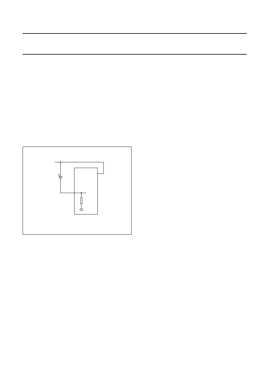
1997 Dec 15
45
Philips Semiconductors
Product specification
8-bit microcontrollers
P83C524; P80C528; P83C528
17.1
Power-on reset
When V
DD
is turned on, and provided its rise-time does not
exceed 10 ms, an automatic reset can be obtained by
connecting the RST pin to V
DD
via a 2.2
µ
F capacitor.
When the power is switched on, the voltage on the RST pin
is equal to V
DD
minus the capacitor voltage, and
decreases from V
DD
as the capacitor charges through the
internal resistor (R
RST
) to ground. The larger the capacitor,
the more slowly V
RST
decreases. V
RST
must remain above
the lower threshold of the Schmitt trigger long enough to
effect a complete reset. The time required is the oscillator
start-up time, plus 2 machine cycles, or 16 x 2048 cycles
of the on-chip watchdog oscillator if it is running, whichever
is longer (see Fig.25).
Fig.25 Power-on reset.
handbook, halfpage
V
DD
V
DD
RST
2.2
µ
F
R RST
MBC474
P83C528

1997 Dec 15
46
Philips Semiconductors
Product specification
8-bit microcontrollers
P83C524; P80C528; P83C528
18 INSTRUCTION SET
The instruction set consists of 49 single-byte, 46 two-byte and 16 three-byte instructions. When using a 12 MHz
oscillator, 64 instructions execute in 1 cycle (1
µ
s) and 45 instructions execute in 2 cycles (2
µ
s). Multiply and divide
instructions execute in 4 cycles (4
µ
s).
Table 30 Instruction set description: Arithmetic operations
MNEMONIC
DESCRIPTION
BYTES
CYCLES
OPCODE
(HEX)
Arithmetic operations
ADD
A,Rr
Add register to A
1
1
2*
ADD
A,direct
Add direct byte to A
2
1
25
ADD
A,@Ri
Add indirect RAM to A
1
1
26, 27
ADD
A,#data
Add immediate data to A
2
1
24
ADDC
A,Rr
Add register to A with carry flag
1
1
3*
ADDC
A,direct
Add direct byte to A with carry flag
2
1
35
ADDC
A,@Ri
Add indirect RAM to A with carry flag
1
1
36, 37
ADDC
A,#data
Add immediate data to A with carry flag
2
1
34
SUBB
A,Rr
Subtract register from A with borrow
1
1
9*
SUBB
A,direct
Subtract direct byte from A with borrow
2
1
95
SUBB
A,@Ri
Subtract indirect RAM from A with borrow
1
1
96, 97
SUBB
A,#data
Subtract immediate data from A with borrow
2
1
94
INC
A
Increment A
1
1
04
INC
Rr
Increment register
1
1
0*
INC
direct
Increment direct byte
2
1
05
INC
@Ri
Increment indirect RAM
1
1
06, 07
DEC
A
Decrement A
1
1
14
DEC
Rr
Decrement register
1
1
1*
DEC
direct
Decrement direct byte
2
1
15
DEC
@Ri
Decrement indirect RAM
1
1
16, 17
INC
DPTR
Increment data pointer
1
2
A3
MUL
AB
Multiply A and B
1
4
A4
DIV
AB
Divide A by B
1
4
84
DA
A
Decimal adjust A
1
1
D4

1997 Dec 15
47
Philips Semiconductors
Product specification
8-bit microcontrollers
P83C524; P80C528; P83C528
Table 31 Instruction set description: Logic operations
MNEMONIC
DESCRIPTION
BYTES
CYCLES
OPCODE
(HEX)
Logic operations
ANL
A,Rr
AND register to A
1
1
5*
ANL
A,direct
AND direct byte to A
2
1
55
ANL
A,@Ri
AND indirect RAM to A
1
1
56, 57
ANL
A,#data
AND immediate data to A
2
1
54
ANL
direct,A
AND A to direct byte
2
1
52
ANL
direct,#data
AND immediate data to direct byte
3
2
53
ORL
A,Rr
OR register to A
1
1
4*
ORL
A,direct
OR direct byte to A
2
1
45
ORL
A,@Ri
OR indirect RAM to A
1
1
46, 47
ORL
A,#data
OR immediate data to A
2
1
44
ORL
direct,A
OR A to direct byte
2
1
42
ORL
direct,#data
OR immediate data to direct byte
3
2
43
XRL
A,Rr
Exclusive-OR register to A
1
1
6*
XRL
A,direct
Exclusive-OR direct byte to A
2
1
65
XRL
A,@Ri
Exclusive-OR indirect RAM to A
1
1
66, 67
XRL
A,#data
Exclusive-OR immediate data to A
2
1
64
XRL
direct,A
Exclusive-OR A to direct byte
2
1
62
XRL
direct,#data
Exclusive-OR immediate data to direct byte
3
2
63
CLR
A
Clear A
1
1
E4
CPL
A
Complement A
1
1
F4
RL
A
Rotate A left
1
1
23
RLC
A
Rotate A left through the carry flag
1
1
33
RR
A
Rotate A right
1
1
03
RRC
A
Rotate A right through the carry flag
1
1
13
SWAP
A
Swap nibbles within A
1
1
C4

1997 Dec 15
48
Philips Semiconductors
Product specification
8-bit microcontrollers
P83C524; P80C528; P83C528
Table 32 Instruction set description: Data transfer
Note
1. MOV A,ACC is not permitted.
MNEMONIC
DESCRIPTION
BYTES
CYCLES
OPCODE
(HEX)
Data transfer
MOV
A,Rr
Move register to A
1
1
E*
MOV
A,direct (note 1)
Move direct byte to A
2
1
E5
MOV
A,@Ri
Move indirect RAM to A
1
1
E6, E7
MOV
A,#data
Move immediate data to A
2
1
74
MOV
Rr,A
Move A to register
1
1
F*
MOV
Rr,direct
Move direct byte to register
2
2
A*
MOV
Rr,#data
Move immediate data to register
2
1
7*
MOV
direct,A
Move A to direct byte
2
1
F5
MOV
direct,Rr
Move register to direct byte
2
2
8*
MOV
direct,direct
Move direct byte to direct
3
2
85
MOV
direct,@Ri
Move indirect RAM to direct byte
2
2
86, 87
MOV
direct,#data
Move immediate data to direct byte
3
2
75
MOV
@RI,A
Move A to indirect RAM
1
1
F6, F7
MOV
@Ri,direct
Move direct byte to indirect RAM
2
2
A6, A7
MOV
@Ri,#data
Move immediate data to indirect RAM
2
1
76, 77
MOV
DPTR,#data 16
Load data pointer with a 16-bit constant
3
2
90
MOVC
A,@A+DPTR
Move code byte relative to DPTR to A
1
2
93
MOVC
A,@A+PC
Move code byte relative to PC to A
1
2
83
MOVX
A,@Ri
Move external RAM (8-bit address) to A
1
2
E2, E3
MOVX
A,@DPTR
Move external RAM (16-bit address) to A
1
2
E0
MOVX
@Ri,A
Move A to external RAM (8-bit address)
1
2
F2, F3
MOVX
@DPTR,A
Move A to external RAM (16-bit address)
1
2
F0
PUSH
direct
Push direct byte onto stack
2
2
C0
POP
direct
Pop direct byte from stack
2
2
D0
XCH
A,Rr
Exchange register with A
1
1
C*
XCH
A,direct
Exchange direct byte with A
2
1
C5
XCH
A,@Ri
Exchange indirect RAM with A
1
1
C6, C7
XCHD
A,@Ri
Exchange LOW-order digit indirect RAM with A
1
1
D6, D7

1997 Dec 15
49
Philips Semiconductors
Product specification
8-bit microcontrollers
P83C524; P80C528; P83C528
Table 33 Instruction set description: Boolean variable manipulation, Program and machine control
MNEMONIC
DESCRIPTION
BYTES
CYCLES
OPCODE
(HEX)
Boolean variable manipulation
CLR
C
Clear carry flag
1
1
C3
CLR
bit
Clear direct bit
2
1
C2
SETB
C
Set carry flag
1
1
D3
SETB
bit
Set direct bit
2
1
D2
CPL
C
Complement carry flag
1
1
B3
CPL
bit
Complement direct bit
2
1
B2
ANL
C,bit
AND direct bit to carry flag
2
2
82
ANL
C,/bit
AND complement of direct bit to carry flag
2
2
B0
ORL
C,bit
OR direct bit to carry flag
2
2
72
ORL
C,/bit
OR complement of direct bit to carry flag
2
2
A0
MOV
C,bit
Move direct bit to carry flag
2
1
A2
MOV
bit,C
Move carry flag to direct bit
2
2
92
Program and machine control
ACALL addr11
Absolute subroutine call
2
2
∑
1addr
LCALL addr16
Long subroutine call
3
2
12
RET
Return from subroutine
1
2
22
RETI
Return from interrupt
1
2
32
AJMP
addr11
Absolute jump
2
2
1addr
LJMP
addr16
Long jump
3
2
02
SJMP
rel
Short jump (relative address)
2
2
80
JMP
@A+DPTR
Jump indirect relative to the DPTR
1
2
73
JZ
rel
Jump if A is zero
2
2
60
JNZ
rel
Jump if A is not zero
2
2
70
JC
rel
Jump if carry flag is set
2
2
40
JNC
rel
Jump if carry flag is not set
2
2
50
JB
bit,rel
Jump if direct bit is set
3
2
20
JNB
bit,rel
Jump if direct bit is not set
3
2
30
JBC
bit,rel
Jump if direct bit is set and clear bit
3
2
10
CJNE
A,direct,rel
Compare direct to A and jump if not equal
3
2
B5
CJNE
A,#data,rel
Compare immediate to A and jump if not equal
3
2
B4
CJNE
Rr,#data,rel
Compare immediate to register and jump if not
equal
3
2
B*
CJNE
@Ri,#data,rel
Compare immediate to indirect and jump if not
equal
3
2
B6, B7
DJNZ
Rr,rel
Decrement register and jump if not zero
2
2
D*
DJNZ
direct,rel
Decrement direct and jump if not zero
3
2
D5
NOP
No operation
1
1
00

1997 Dec 15
50
Philips Semiconductors
Product specification
8-bit microcontrollers
P83C524; P80C528; P83C528
Table 34 Description of the mnemonics in the Instruction set
MNEMONIC
DESCRIPTION
Data addressing modes
Rr
working register R0-R7.
direct
128 internal RAM locations and any special function register (SFR).
@Ri
indirect internal RAM location addressed by register R0 or R1 of the actual register bank.
#data
8-bit constant included in instruction.
#data 16
16-bit constant included as bytes 2 and 3 of instruction.
bit
direct addressed bit in internal RAM or SFR.
addr16
16-bit destination address. Used by LCALL and LJMP. The branch will be anywhere within the
64 kbytes program memory address space.
addr11
11-bit destination address. Used by ACALL and AJMP. The branch will be within the same 2 kbytes
page of program memory as the first byte of the following instruction.
rel
Signed (two's complement) 8-bit offset byte. Used by SJMP and all conditional jumps. Range is
-
128 to +127 bytes relative to first byte of the following instruction.
Hexadecimal opcode cross-reference
*
8, 9, A, B, C, D, E, F.
∑
11, 31, 51, 71, 91, B1, D1, F1.
01, 21, 41, 61, 81, A1, C1, E1.

1997
Dec
15
51
Philips Semiconductors
Product specification
8-bit microcontrollers
P83C524; P80C528; P83C528
This text is here in white to force landscape pages to be rotated correctly when browsing through the pdf in the Acrobat reader.This text is here in
_
white to force landscape pages to be rotated correctly when browsing through the pdf in the Acrobat reader.This text is here inThis text is here in
white to force landscape pages to be rotated correctly when browsing through the pdf in the Acrobat reader. white to force landscape pages to be ...
T
able 35
Instruction map
Note
1. MOV A, ACC is not a valid instruction.
First hexadecimal character of opcode
Second hexadecimal character of opcode
0
1
2
3
4
5
6
7
8
9
A B C D E F
0
NOP
AJMP
addr11
LJMP
addr16
RR
A
INC
A
INC
direct
INC @Ri
INC Rr
0
1
0
1
2
3
4
5
6
7
1
JBC
bit,rel
ACALL
addr11
LCALL
addr16
RRC
A
DEC
A
DEC
direct
DEC @Ri
DEC Rr
0
1
0
1
2
3
4
5
6
7
2
JB
bit,rel
AJMP
addr11
RET
RL
A
ADD
A,#data
ADD
A,direct
ADD A,@Ri
ADD A,Rr
0
1
0
1
2
3
4
5
6
7
3
JNB
bit,rel
ACALL
addr11
RETI
RLC
A
ADDC
A,#data
ADDC
A,direct
ADDC A,@Ri
ADDC A,Rr
0
1
0
1
2
3
4
5
6
7
4
JC
rel
AJMP
addr11
ORL
direct,A
ORL
direct,#data
ORL
A,#data
ORL
A,direct
ORL A,@Ri
ORL A,Rr
0
1
0
1
2
3
4
5
6
7
5
JNC
rel
ACALL
addr11
ANL
direct,A
ANL
direct,#data
ANL
A,#data
ANL
A,direct
ANL A,@Ri
ANL A,Rr
0
1
0
1
2
3
4
5
6
7
6
JZ
rel
AJMP
addr11
XRL
direct,A
XRL
direct,#data
XRL
A,#data
XRL
A,direct
XRL A,@Ri
XRL A,Rr
0
1
0
1
2
3
4
5
6
7
7
JNZ
rel
ACALL
addr11
ORL
C,bit
JMP
@A+DPTR
MOV
A,#data
MOV
direct,#data
MOV @Ri,#data
MOV Rr,#data
0
1
0
1
2
3
4
5
6
7
8
SJMP
rel
AJMP
addr11
ANL
C,bit
MOVC
A,@A+PC
DIV
AB
MOV
direct,direct
MOV direct,@Ri
MOV direct,Rr
0
1
0
1
2
3
4
5
6
7
9
MOV
DTPR,#data16
ACALL
addr11
MOV
bit,C
MOVC
A,@A+DPTR
SUBB
A,#data
SUBB
A,direct
SUBB A,@Ri
SUB A,Rr
0
1
0
1
2
3
4
5
6
7
A
ORL
C,/bit
AJMP
addr11
MOV
bit,C
INC
DPTR
MUL
AB
MOV @Ri,direct
MOV Rr,direct
0
1
0
1
2
3
4
5
6
7
B
ANL
C,/bit
ACALL
addr11
CPL
bit
CPL
C
CJNE
A,#data,rel
CJNE
A,direct,rel
CJNE @Ri,#data,rel
CJNE Rr,#data,rel
0
1
0
1
2
3
4
5
6
7
C
PUSH
direct
AJMP
addr11
CLR
bit
CLR
C
SWAP
A
XCH
A,direct
XCH A,@Ri
XCH A,Rr
0
1
0
1
2
3
4
5
6
7
D
POP
direct
ACALL
addr11
SETB
bit
SETB
C
DA
A
DJNZ
direct,rel
XCHD A,@Ri
DJNZ Rr,rel
0
1
0
1
2
3
4
5
6
7
E
MOVX
A,@DTPR
AJMP
addr11
MOVX A,@Ri
CLR
A
MOV
A,direct
(1)
MOV A,@Ri
MOV A,Rr
0
1
0
1
0
1
2
3
4
5
6
7
F
MOVX
@DTPR,A
ACALL
addr11
MOVX @Ri,A
CPL
A
MOV
direct,A
MOV @Ri,A
MOV Rr,A
0
1
0
1
0
1
2
3
4
5
6
7

1997 Dec 15
52
Philips Semiconductors
Product specification
8-bit microcontrollers
P83C524; P80C528; P83C528
19 LIMITING VALUES
In accordance with the Absolute Maximum System (IEC 134)
SYMBOL
PARAMETER
MIN.
MAX.
UNIT
V
DD
supply voltage range
-
0.5
+6.0
V
V
I
all input voltages
-
0.5
V
DD
+0.5
V
P
tot
total power dissipation
-
1
W
T
stg
storage temperature range
-
65
+150
∞
C
T
amb
operating ambient temperature range:
version xBx
0
+70
∞
C
version xFx
-
40
+85
∞
C
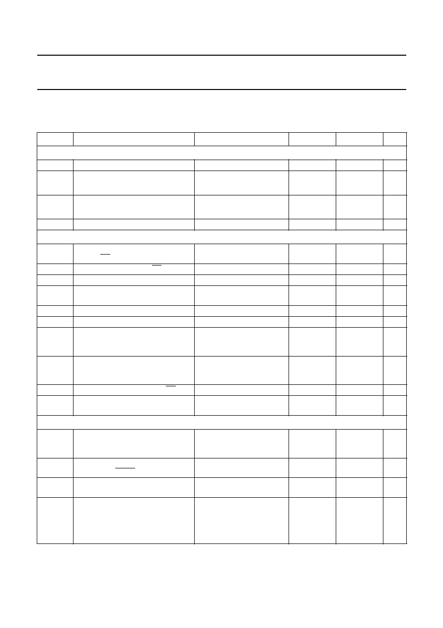
1997 Dec 15
53
Philips Semiconductors
Product specification
8-bit microcontrollers
P83C524; P80C528; P83C528
20 DC CHARACTERISTICS
V
DD
= 5 V
±
10%; V
SS
= 0 V; T
amb
= 0 to +70
∞
C;
-
40 to +85
∞
C. All voltages with respect to V
SS
unless otherwise
specified.
SYMBOL
PARAMETER
CONDITIONS
MIN.
MAX.
UNIT
Supply
V
DD
supply voltage range
4.5
5.5
V
I
DD
supply current operating modes,
note 1
V
DDmax
, 16 MHz
V
DDmax
, 24 MHz
-
33
43
mA
mA
I
ID
supply current Idle mode, note 2
V
DDmax
, 16 MHz
V
DDmax
, 24MHz
-
6
7.5
mA
mA
I
PD
supply current Power
-
down mode
2 V
V
DD
V
DDmax
; note 3
-
100
µ
A
Inputs
V
IL
LOW level input voltage
(except EA, P1.6, P1.7)
-
0.5
0.2 V
DD
-
0.1
V
V
IL1
LOW level input voltage EA
-
0.5
0.2 V
DD
-
0.3
V
V
IL2
LOW level input voltage P1.6, P1.7
note 6
-
0.5
0.3 V
DD
V
V
IH
HIGH level input voltage
(except RST, XTAL1, P1.6, P1.7)
0.2 V
DD
+0.9
V
DD
+0.5
V
V
IH1
HIGH level input voltage RST, XTAL1
0.7 V
DD
V
DD
+0.5
V
V
IH2
HIGH level input voltage P1.6, P1.7
note 6
0.7 V
DD
5.5
V
I
IL
LOW level input current
Ports 1, 2 and 3
(except P1.6 and P1.7)
V
I
= 0.45 V
-
-
50
µ
A
I
TL
input current HIGH-to-LOW transition
Ports 1, 2 and 3
(except P1.6 and P1.7)
V
I
= 2.0 V
-
-
650
µ
A
I
LI1
input leakage current Port 0, EA
0.45
<
V
I
<
V
DD
-
±
10
µ
A
I
LI2
input leakage current P1.6 and P1.7
0 V
<
V
I
<
5.5 V
0 V
<
V
DD
<
5.5 V
-
±
10
µ
A
Outputs
V
OL
LOW level output voltage
Ports 1, 2 and 3
(except P1.6 and P1.7)
I
OL
= 1.6 mA; notes 6 and 7
-
0.45
V
V
OL1
LOW level output voltage
Port 0, ALE, PSEN
I
OL
= 3.2 mA; notes 4 and 7
-
0.45
V
V
OL2
LOW level output voltage
P1.6 and P1.7
I
OL
= 3.0 mA; note 7
-
0.40
V
V
OH
HIGH level output voltage
Ports 1, 2 and 3
(except P1.6 and P1.7)
I
OH
=
-
60
µ
A;
V
DD
= 5 V
±
10%
I
OH
=
-
25
µ
A
I
OH
=
-
10
µ
A
2.4
0.75 V
DD
0.9 V
DD
-
-
-
V

1997 Dec 15
54
Philips Semiconductors
Product specification
8-bit microcontrollers
P83C524; P80C528; P83C528
Notes to the DC characteristics
1. Conditions for:
a) The operating supply current is measured with all output pins disconnected; XTAL1 driven with t
r
= t
f
= 5 ns;
V
IL
= V
SS
+0.5 V; V
IH
= V
DD
-
0.5 V; XTAL2 not connected; EA = RST = Port 0 = P1.6 = P1.7 = V
DD
;
the WDT is disabled (by the external RESET).
2. Conditions for:
a) The Idle mode supply current is measured with all output pins disconnected; XTAL1 driven with t
r
= t
f
= 5 ns;
V
IL
= V
SS
+0.5 V; V
IH
= V
DD
-
0.5 V; XTAL2 not connected; the WDT is disabled; EA = RST = V
SS
;
Port 0 = P1.6 = P1.7 = V
DD
.
3. Conditions for:
a) The Power-down current is measured with all output pins disconnected; XTAL2 not connected;
WDT is disabled; EA = RST = XTAL1 = V
SS
; Port 0 = P1.6 = P1.7 = V
DD
.
4. Capacitive loading on Port 0 and Port 2 may cause spurious noise pulses to be superimposed on the LOW level
output voltage of ALE, Port 1 and Port 3. The noise is due to external bus capacitance discharging into the Port 0
and Port 2 pins when these pins make a HIGH-to-LOW transition during bus operations. In the worst cases
(capacitive loading
>
100pF), the noise pulse on the ALE line may exceed 0.8 V. In such cases it may be desirable
to qualify ALE with a Schmitt Trigger, or use an address latch with a Schmitt Trigger STROBE input.
5. Capacitive loading on Port 0 and Port 2 may cause the HIGH level output voltage on ALE and PSEN to momentarily
fall below the 0.9 V
DD
specification when the address bits are stabilizing.
6. The input threshold voltage of P1.6 and P1.7 (SIO1) meets the I
2
C specification, so a voltage below 0.3 V
DD
will be
recognized as a logic 0 while an input above 0.7 V
DD
will be recognized as a logic 1.
7. Under steady state (non-transient) conditions, I
OL
must be externally limited as follows:
a) Maximum I
OL
per port pin:10 mA.
b) Maximum I
OL
per 8-bit port:- Port 0: 26 mA; Ports 1, 2 and 3: 15 mA.
c) Maximum total I
OL
for all output pins: 71 mA. If I
OL
exceeds the test condition,
V
OL
may exceed the related specification.
d) Pins are not guaranteed to sink current greater than the listed test conditions.
8. I
DD
max. at other frequencies can be derived from Fig.26 where f is the external oscillator frequency in MHz;
I
DD
max. is given in mA.
V
OH1
HIGH level output voltage
Port0in in external bus mode,
ALE, PSEN, RST
I
OH
=
-
800
µ
A;
V
DD
= 5 V
±
10%
I
OH
=
-
300
µ
A;
I
OH
=
-
80
µ
A; note 5
2.4
0.75V
DD
0.9V
DD
-
-
-
V
R
RST
RST pull
-
down resistor
50
150
k
C
I/O
I/O pin capacitance
test frequency = 1 MHz;
T
amb
= 25
∞
C
-
10
pF
SYMBOL
PARAMETER
CONDITIONS
MIN.
MAX.
UNIT

1997 Dec 15
55
Philips Semiconductors
Product specification
8-bit microcontrollers
P83C524; P80C528; P83C528
Fig.26 I
DD
as a function of frequency.
Valid only within frequency specifications of device under test.
handbook, full pagewidth
0
8
24
40
50
30
10
0
20
MBC478
16
f (MHz)
I DD
(mA)
MAX ACTIVE MODE
TYP ACTIVE MODE
MAX IDLE MODE
TYP IDLE MODE

1997 Dec 15
56
Philips Semiconductors
Product specification
8-bit microcontrollers
P83C524; P80C528; P83C528
21 AC CHARACTERISTICS
21.1
AC Characteristics 16 MHz version
See notes 1, 2 and 3 in Section 21.2; Cl = 100 pF for Port 0, ALE and PSEN; C
L
= 80 pF for all other outputs unless
otherwise specified.
SYMBOL
PARAMETER
16 MHZ
VARIABLE CLOCK
UNIT
MIN.
MAX.
MIN.
MAX.
External program memory
t
LHLL
ALE pulse duration
85
-
2 t
CK
-
40
-
ns
t
AVLL
address set-up time to ALE
8
-
t
CK
-
55
-
ns
t
LLAX
address hold time after ALE
28
-
t
CK
-
35
-
ns
t
LLIV
time from ALE to valid instruction input
-
150
-
4 t
CK
-
100
ns
t
LLPL
time from ALE to control pulse PSEN
23
-
t
CK
-
40
-
ns
t
PLPH
control pulse duration PSEN
143
-
3 t
CK
-
45
-
ns
t
PLIV
time from PSEN to valid instruction input
-
83
-
3 t
CK
-
105
ns
t
PXIX
input instruction hold time after PSEN
0
-
0
-
ns
t
PXIZ
input instruction float delay after PSEN
-
38
-
t
CK
-
25
ns
t
AVIV
address to valid instruction input
-
208
-
5 t
CK
-
105
ns
t
PLAZ
address float time to PSEN
-
10
-
10
ns
External data memory
t
LHLL
ALE pulse duration
85
-
2 t
CK
-
40
-
ns
t
AVLL
address set-up time to ALE
8
-
t
CK
-
55
-
ns
t
LLAX
address hold time after ALE
28
-
t
CK
-
35
-
ns
t
RLRH
RD pulse duration
275
-
6 t
CK
-
100
-
ns
t
WLWH
WR pulse duration
275
-
6 t
CK
-
100
-
ns
t
RLDV
RD to valid data input
-
148
-
5 t
CK
-
165
ns
t
RHDX
data hold time after RD
0
-
0
-
ns
t
RHDZ
data float delay after RD
-
55
-
2 t
CK
-
70
ns
t
LLDZ
time from ALE to valid data input
-
350
-
8 t
CK
-
150
ns
t
AVDV
address to valid data input
-
398
-
9 t
CK
-
165
ns
t
LLWL
time from ALE to RD or WR
138
238
3 t
CK
-
50
3 t
CK
+50
ns
t
AVWL
time from address to RD or WR
120
-
4 t
CK
-
130
-
ns
t
WHLH
time from RD or WR HIGH to ALE HIGH
23
103
t
CK
-
40
t
CK
+ 40
ns
t
QVWX
data valid to WR transition
3
-
t
CK
-
60
-
ns
t
QVWH
data set-up time before WR
288
-
7 t
CK
-
150
-
ns
t
WHQX
data hold time after WR
13
-
t
CK
-
50
-
ns
t
RLAZ
address float delay after RD
-
0
-
0
ns

1997 Dec 15
57
Philips Semiconductors
Product specification
8-bit microcontrollers
P83C524; P80C528; P83C528
21.2
AC Characteristics 24 MHz version
See notes 1, 2 and 3.; Cl = 100 pF for Port 0, ALE and PSEN; C
L
= 80 pF for all other outputs unless otherwise
specified.
Notes to the AC Characteristics 16 and 24 MHz versions
1. For the AC Characteristics the following conditions are valid:
a) P83C52x EBx: V
DD
= 5 V
±
10%; V
SS
= 0 V; T
amb
= 0 to +70
∞
C; t
CK
min. = 63 ns
b) P83C52x EFx: V
DD
= 5 V
±
10%; V
SS
= 0 V; T
amb
=
-
40 to +85
∞
C; t
CK
min. = 63 ns.
2. t
CK
min. = 1/f max. (maximum operating frequency); t
CK
= clock period (see section for timing symbol definitions).
3. The maximum operating frequency is limited to 16/24 MHz and the minimum to 3.5 MHz (all versions Ixx/Exx).
SYMBOL
PARAMETER
24 MHZ
VARIABLE CLOCK
UNIT
MIN.
MAX.
MIN.
MAX.
External program memory
t
LHLL
ALE pulse duration
43
-
2 t
CK
-
40
-
ns
t
AVLL
address set-up time to ALE
17
-
t
CK
-
25
-
ns
t
LLAX
address hold time after ALE
17
-
t
CK
-
25
-
ns
t
LLIV
time from ALE to valid instruction input
-
102
-
4 t
CK
-
65
ns
t
LLPL
time from ALE to control pulse PSEN
17
-
t
CK
-
25
-
ns
t
PLPH
control pulse duration PSEN
80
-
3 t
CK
-
45
-
ns
t
PLIV
time from PSEN to valid instruction input
-
65
-
3 t
CK
-
60
ns
t
PXIX
input instruction hold time after PSEN
0
-
0
-
ns
t
PXIZ
input instruction float delay after PSEN
-
17
-
t
CK
-
25
ns
t
AVIV
address to valid instruction input
-
128
-
5 t
CK
-
80
ns
t
PLAZ
address float time to PSEN
-
10
-
10
ns
External data memory
t
LHLL
ALE pulse duration
43
-
2 t
CK
-
40
-
ns
t
AVLL
address set-up time to ALE
17
-
t
CK
-
25
-
ns
t
LLAX
address hold time after ALE
17
-
t
CK
-
25
-
ns
t
RLRH
RD pulse duration
150
-
6 t
CK
-
100
-
ns
t
WLWH
WR pulse duration
150
-
6 t
CK
-
100
-
ns
t
RLDV
RD to valid data input
-
118
-
5 t
CK
-
90
ns
t
RHDX
data hold time after RD
0
-
0
-
ns
t
RHDZ
data float delay after RD
-
55
-
2 t
CK
-
28
ns
t
LLDZ
time from ALE to valid data input
-
183
-
8 t
CK
-
150
ns
t
AVDV
address to valid data input
-
210
-
9 t
CK
-
165
ns
t
LLWL
time from ALE to RD or WR
75
175
3 t
CK
-
50
3 t
CK
+50
ns
t
AVWL
time from address to RD or WR
92
-
4 t
CK
-
75
-
ns
t
WHLH
time from RD or WR HIGH to ALE HIGH
17
67
t
CK
-
25
t
CK
+ 25
ns
t
QVWX
data valid to WR transition
12
-
t
CK
-
30
-
ns
t
QVWH
data set-up time before WR
162
-
7 t
CK
-
130
-
ns
t
WHQX
data hold time after WR
17
-
t
CK
-
25
-
ns
t
RLAZ
address float delay after RD
-
0
-
0
ns

1997 Dec 15
58
Philips Semiconductors
Product specification
8-bit microcontrollers
P83C524; P80C528; P83C528
22 I
2
C CHARACTERISTICS (BIT-LEVEL)
Notes
1. At f
CLK
= 3.5 MHz, this evaluates to 14
◊
286 ns = 4
µ
s, i.e. the bit-level I
2
C interface can respond to the I
2
C protocol
for f
CLK
3.5 MHz.
2. This parameter is determined by the user software, it has to comply with the I
2
C specification.
3. This value gives the auto-clock pulse length which meets the I
2
C specification for the specified XTAL1 clock
frequency range. Alternatively, the SCL pulse may be timed by software.
4. Spikes on SDA and SCL lines with a duration of less than 4
◊
f
CLK
will be filtered out.
5. The RISE time is determined by the external bus line capacitance and pull-up resistor, it must be
1
µ
s.
6. The maximum capacitance on bus lines SDA and SCL is 400 pF.
SYMBOL
PARAMETER
INPUT
OUTPUT
I
2
C SPEC
UNIT
SCL timing
t
HD;STA
START condition hold time
14 t
CK
; note 1
note 2
4.0
µ
s
t
LOW
SCL LOW time
16 t
CK
note 2
4.7
µ
s
t
HIGH
SCL HIGH time
14 t
CK
; note 1
80 t
CK
; note 3
4.0
µ
s
t
RC
SCL RISE time
1; note 4
note 5
1.0
µ
s
t
FC
SCL FALL time
0.3; note 4
0.3; note 6
0.3
µ
s
SDA timing
t
SU;DAT
data set-up time
250 ns
note 2
250
ns
t
HD;DAT
data hold time
0 ns
note 2
0
ns
t
SU;STA
repeated START set-up time
14 t
CK
; note 1
note 2
4.7
µ
s
t
SU;STO
STOP condition set
-
up time
14 t
CK
; note 1
note 2
4.0
µ
s
t
BUF
bus free time
14 t
CK
; note 1
note 2
4.7
µ
s
t
RD
SDA RISE time
1; note 4
note 5
1.0
µ
s
t
FD
SDA FALL time
300 ns; note 4
0.3; note 6
0.3
µ
s
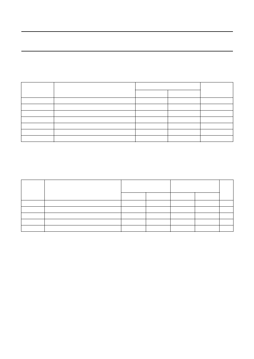
1997 Dec 15
59
Philips Semiconductors
Product specification
8-bit microcontrollers
P83C524; P80C528; P83C528
23 XTAL1 CHARACTERISTICS
Oscillator circuitry: crystal capacitors: C1 = C2 = 20 pF (see Fig.31).
Table 36 External clock drive XTAL
24 SERIAL PORT CHARACTERISTICS
See Table 37 and Fig.32.
Table 37 Serial Port Timing: Shift Register Mode
V
DD
= 5 V
±
10%; V
SS
= 0 V; T
amb
= 0
∞
C to 70
∞
C; Load Capacitance = 80 pF
SYMBOL
PARAMETER
VARIABLE CLOCK
UNIT
MIN.
MAX.
f
CLK
clock frequency
3.5
24
MHz
t
CK
clock period
42
286
ns
t
HIGH
HIGH time
17
t
CK
-
t
LOW
ns
t
LOW
LOW time
17
t
CK
-
t
HIGH
ns
t
r
RISE time
-
5
ns
t
f
FALL time
-
5
ns
t
CY
cycle time (t
CY
= 12 t
CK
)
0.5
3.43
µ
s
SYMBOL
PARAMETER
24 MHZ OSCILLATOR
VARIABLE
OSCILLATOR
UNIT
MIN.
MAX.
MIN.
MAX.
t
XLXL
Serial Port clock cycle time
0.5
-
12 t
CK
-
µ
s
t
QVXH
output data setup to clock rising edge
283
-
10 t
CK
-
133
-
ns
t
XHQX
output data hold after clock rising edge
23
-
2 t
CK
-
60
-
ns
t
XHDX
input data hold after clock rising edge
0
-
0
-
ns
t
XHDV
clock rising edge to input data valid
-
283
-
10 t
CK
-
133
ns
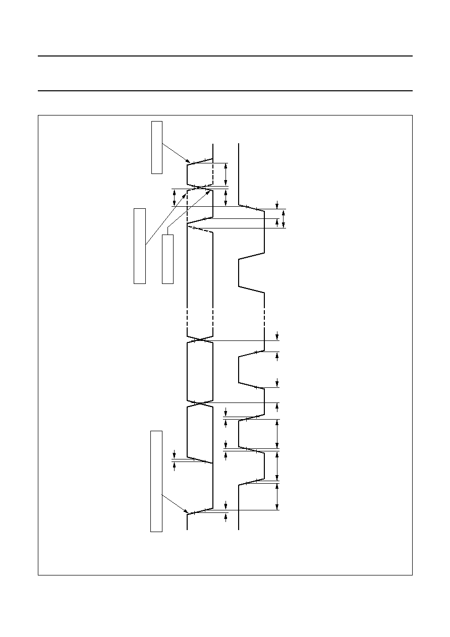
1997
Dec
15
60
Philips Semiconductors
Product specification
8-bit microcontrollers
P83C524; P80C528; P83C528
This text is here in white to force landscape pages to be rotated correctly when browsing through the pdf in the Acrobat reader.This text is here in
_
white to force landscape pages to be rotated correctly when browsing through the pdf in the Acrobat reader.This text is here inThis text is here in
white to force landscape pages to be rotated correctly when browsing through the pdf in the Acrobat reader. white to force landscape pages to be ...
25
TIMING DIAGRAMS
handbook, full pagewidth
t RD
t FD
t RC
t FC
t HD;STA
t LOW
t HIGH
t SU;DAT1
t HD;DAT
t SU;DAT2
t SU;DAT3
0.7 VDD
0.3 VDD
t SU;STO
t BUF
tSU;STA
SDA
(input / output)
SCL
(input / output)
START condition
repeated START condition
STOP condition
START or repeated START condition
0.7 VDD
0.3 VDD
MBC482
Fig.27 I
2
C interface timing.

1997 Dec 15
61
Philips Semiconductors
Product specification
8-bit microcontrollers
P83C524; P80C528; P83C528
Fig.28 External program memory read cycle.
handbook, full pagewidth
MBC483 - 1
t LHLL
t AVLL
t LLPL
t PLPH
t LLIV
t PLIV
t LLAX
t PLAZ
t PXIX
t PXIZ
INSTR IN
A0 - A7
A0 - A7
A8 - A15
A8 - A15
ALE
PSEN
PORT 0
PORT 2
t AVIV

1997
Dec
15
62
Philips Semiconductors
Product specification
8-bit microcontrollers
P83C524; P80C528; P83C528
This text is here in white to force landscape pages to be rotated correctly when browsing through the pdf in the Acrobat reader.This text is here in
_
white to force landscape pages to be rotated correctly when browsing through the pdf in the Acrobat reader.This text is here inThis text is here in
white to force landscape pages to be rotated correctly when browsing through the pdf in the Acrobat reader. white to force landscape pages to be ...
handbook, full pagewidth
MBC485 - 1
ALE
PSEN
PORT 0
PORT 2
RD
t AVWL
tAVLL
tLLAX
t LLWL
t RLRH
RHDX
t
t WHLH
A0 - A7
from RI or DPL
DATA IN
A0 - A7 from PCL
INSTR IN
A8 - A15 from PCH
P2.0 - P2.7 or A8 - A15 from DPH
RHDZ
t
t AVDV
RLDV
t
t LLDV
Fig.29 External data memory read cycle.

1997
Dec
15
63
Philips Semiconductors
Product specification
8-bit microcontrollers
P83C524; P80C528; P83C528
This text is here in white to force landscape pages to be rotated correctly when browsing through the pdf in the Acrobat reader.This text is here in
_
white to force landscape pages to be rotated correctly when browsing through the pdf in the Acrobat reader.This text is here inThis text is here in
white to force landscape pages to be rotated correctly when browsing through the pdf in the Acrobat reader. white to force landscape pages to be ...
handbook, full pagewidth
MBC486 - 1
ALE
PSEN
PORT 0
PORT 2
WR
t AVWL
t
AVLL
t
LLAX
QVWX
t
t LLWL
t WLWH
WHQX
t
t WHLH
A0 - A7
from RI or DPL
DATA OUT
A0 - A7 from PCL
INSTR IN
A8 - A15 from PCH
P2.0 - P2.7 or A8 - A15 from DPH
t QVWH
Fig.30 External data memory write cycle.

1997 Dec 15
64
Philips Semiconductors
Product specification
8-bit microcontrollers
P83C524; P80C528; P83C528
handbook, full pagewidth
MBC480
2.0 V
0.8 V
2.4 V
0.45 V
2.0 V
0.8 V
2.4 V
0.45 V
float
(b)
(a)
2.4 V
0.45 V
2.0 V
0.8 V
2.0 V
0.8 V
test points
Fig.31 AC testing input, output waveform (a) and float waveform (b).
AC testing inputs are driven at 2.4 V for a logic 1 and 0.45 V for a logic 0. Timing measurements
are taken at 2.0 V for a logic 1 and 0.8 V for logic 0 see (a). The float state is defined as the point
at which a Port 0 pin sinks 3.2 mA or sources 400
µ
A at the voltage test levels see (b).
Fig.32 External clock drive XTAL1.
See Table 36.
handbook, full pagewidth
MBC479
t HIGH
t LOW
t CK
t r
t f
VIH1
V IH1
0.8 V
0.8 V
VIH1
VIH1
0.8 V
0.8 V

1997 Dec 15
65
Philips Semiconductors
Product specification
8-bit microcontrollers
P83C524; P80C528; P83C528
Fig.33 Shift register mode timing waveforms.
See Table 37.
handbook, full pagewidth
MBC475
INSTRUCTION
ALE
CLOCK
8
7
6
5
4
3
2
1
0
VALID
WRITE TO SBUF
OUTPUT DATA
CLEAR RI
INPUT DATA
t XLXL
tXHQX
t QVXH
tXHDV
tXHDX
SET RI
SET TI
VALID
VALID
VALID
VALID
VALID
VALID
VALID

1997 Dec 15
66
Philips Semiconductors
Product specification
8-bit microcontrollers
P83C524; P80C528; P83C528
Fig.34 Instruction cycle timing.
andbook, full pagewidth
MBC487 - 1
P1 P2
S1
P1 P2
S2
P1 P2
S3
P1 P2
S4
P1 P2
S5
P1 P2
S6
P1 P2
S1
P1 P2
S2
P1 P2
S3
P1 P2
S4
P1 P2
S5
P1 P2
S6
one machine cycle
one machine cycle
XTAL1
INPUT
address
A0 - A7
inst.
in
address
A0 - A7
inst.
in
address
A0 - A7
inst.
in
address
A0 - A7
inst.
in
address A8 - A15
address A8 - A15
address A8 - A15
address A8 - A15
address
A0 - A7
inst.
in
address
A0 - A7
inst.
in
address
A0 - A7
data output or data input
address A8 - A15
address A8 - A15 or Port 2 out
address A8 - A15
old data
new data
sampling time of I/O port pins during input (including INT0 and INT1)
SERIAL
PORT
CLOCK
PORT
INPUT
PORT
OUTPUT
PORT 2
BUS
(PORT 0)
read or
write of
external data
memory
PORT 2
BUS
(PORT 0)
external
program
memory
fetch
WR
RD
only active
during a write
to external
data memory
only active
during a read
from external
data memory
PSEN
ALE
dotted lines
are valid when
RD or WR are
active

1997 Dec 15
67
Philips Semiconductors
Product specification
8-bit microcontrollers
P83C524; P80C528; P83C528
25.1
Timing symbol definitions
Oscillator:
f
CLK
= clock frequency
t
CK
= clock period
Timing symbols (acronyms):
Each timing symbol has five characters. The first character
is always a 't' (= time). the remaining four characters of the
symbol (typed in subscript), depending on their relative
positions, indicate the name of a signal or the logical status
of that signal. the designations are as follows:
A =address
C = clock
D = input data
H = logic level HIGH
I = instruction (program memory contents)
L = Logic level LOW or ALE
P = PSEN
Q = output data
R = RD signal
t = time
V = valid
W = WR signal
X = no longer a valid logic level
Z = float
Examples:
t
AVLL
= time for address valid to ALE LOW
t
LLPL
= time for ALE LOW to PSEN LOW

1997 Dec 15
68
Philips Semiconductors
Product specification
8-bit microcontrollers
P83C524; P80C528; P83C528
26 PACKAGE OUTLINES
UNIT
A
max.
1
2
b
1
c
D
E
e
M
H
L
REFERENCES
OUTLINE
VERSION
EUROPEAN
PROJECTION
ISSUE DATE
IEC
JEDEC
EIAJ
mm
inches
DIMENSIONS (inch dimensions are derived from the original mm dimensions)
SOT129-1
92-11-17
95-01-14
A
min.
A
max.
b
Z
max.
w
M
E
e
1
1.70
1.14
0.53
0.38
0.36
0.23
52.50
51.50
14.1
13.7
3.60
3.05
0.254
2.54
15.24
15.80
15.24
17.42
15.90
2.25
4.7
0.51
4.0
0.067
0.045
0.021
0.015
0.014
0.009
2.067
2.028
0.56
0.54
0.14
0.12
0.01
0.10
0.60
0.62
0.60
0.69
0.63
0.089
0.19
0.020
0.16
051G08
MO-015AJ
M
H
c
(e )
1
M
E
A
L
seating plane
A
1
w
M
b
1
e
D
A
2
Z
40
1
21
20
b
E
pin 1 index
0
5
10 mm
scale
Note
1. Plastic or metal protrusions of 0.25 mm maximum per side are not included.
(1)
(1)
(1)
DIP40: plastic dual in-line package; 40 leads (600 mil)
SOT129-1

1997 Dec 15
69
Philips Semiconductors
Product specification
8-bit microcontrollers
P83C524; P80C528; P83C528
UNIT
A
A
min.
max.
max.
max. max.
1
A
4
b
p
E
(1)
(1)
(1)
e
H
E
Z
y
w
v
REFERENCES
OUTLINE
VERSION
EUROPEAN
PROJECTION
ISSUE DATE
IEC
JEDEC
EIAJ
mm
4.57
4.19
0.51
3.05
0.53
0.33
0.021
0.013
16.66
16.51
1.27
17.65
17.40
0.51
2.16
45
o
0.18
0.10
0.18
DIMENSIONS (millimetre dimensions are derived from the original inch dimensions)
Note
1. Plastic or metal protrusions of 0.01 inches maximum per side are not included.
SOT187-2
D
(1)
16.66
16.51
H
D
17.65
17.40
E
Z
2.16
D
b
1
0.81
0.66
k
1.22
1.07
k
1
0.180
0.165
0.020
0.12
A
3
0.25
0.01
0.656
0.650
0.05
0.695
0.685
0.020
0.085
0.007 0.004
0.007
L
p
1.44
1.02
0.057
0.040
0.656
0.650
0.695
0.685
e
E
e
D
16.00
14.99
0.630
0.590
16.00
14.99
0.630
0.590
0.085
0.032
0.026
0.048
0.042
29
39
44
1
6
7
17
28
18
40
detail X
(A )
3
b
p
w
M
A
1
A
A
4
L
p
b
1
k
1
k
X
y
e
E
B
D
H
E
e
E
H
v
M
B
D
Z D
A
Z E
e
v
M
A
pin 1 index
112E10
MO-047AC
0
5
10 mm
scale
92-11-17
95-02-25
inches
PLCC44: plastic leaded chip carrier; 44 leads
SOT187-2
D
e

1997 Dec 15
70
Philips Semiconductors
Product specification
8-bit microcontrollers
P83C524; P80C528; P83C528
UNIT
A
1
A
2
A
3
b
p
c
E
(1)
e
H
E
L
L
p
Q
Z
y
w
v
REFERENCES
OUTLINE
VERSION
EUROPEAN
PROJECTION
ISSUE DATE
IEC
JEDEC
EIAJ
mm
0.25
0.05
1.85
1.65
0.25
0.40
0.20
0.25
0.14
10.1
9.9
0.8
1.3
12.9
12.3
0.85
0.75
1.2
0.8
10
0
o
o
0.15
0.1
0.15
DIMENSIONS (mm are the original dimensions)
Note
1. Plastic or metal protrusions of 0.25 mm maximum per side are not included.
0.95
0.55
SOT307-2
92-11-17
95-02-04
D
(1)
(1)
(1)
10.1
9.9
H
D
12.9
12.3
E
Z
1.2
0.8
D
e
E
B
11
c
E
H
D
ZD
A
Z E
e
v
M
A
X
1
44
34
33
23
22
12
y
A
1
A
L
p
Q
detail X
L
(A )
3
A
2
pin 1 index
D
H
v
M
B
b
p
b
p
w
M
w
M
0
2.5
5 mm
scale
QFP44: plastic quad flat package; 44 leads (lead length 1.3 mm); body 10 x 10 x 1.75 mm
SOT307-2
A
max.
2.10

1997 Dec 15
71
Philips Semiconductors
Product specification
8-bit microcontrollers
P83C524; P80C528; P83C528
27 SOLDERING
27.1
Introduction
There is no soldering method that is ideal for all IC
packages. Wave soldering is often preferred when
through-hole and surface mounted components are mixed
on one printed-circuit board. However, wave soldering is
not always suitable for surface mounted ICs, or for
printed-circuits with high population densities. In these
situations reflow soldering is often used.
This text gives a very brief insight to a complex technology.
A more in-depth account of soldering ICs can be found in
our
"IC Package Databook" (order code 9398 652 90011).
27.2
DIP
27.2.1
S
OLDERING BY DIPPING OR BY WAVE
The maximum permissible temperature of the solder is
260
∞
C; solder at this temperature must not be in contact
with the joint for more than 5 seconds. The total contact
time of successive solder waves must not exceed
5 seconds.
The device may be mounted up to the seating plane, but
the temperature of the plastic body must not exceed the
specified maximum storage temperature (T
stg max
). If the
printed-circuit board has been pre-heated, forced cooling
may be necessary immediately after soldering to keep the
temperature within the permissible limit.
27.2.2
R
EPAIRING SOLDERED JOINTS
Apply a low voltage soldering iron (less than 24 V) to the
lead(s) of the package, below the seating plane or not
more than 2 mm above it. If the temperature of the
soldering iron bit is less than 300
∞
C it may remain in
contact for up to 10 seconds. If the bit temperature is
between 300 and 400
∞
C, contact may be up to 5 seconds.
27.3
PLCC and QFP
27.3.1
R
EFLOW SOLDERING
Reflow soldering techniques are suitable for all PLCC and
QFP packages.
The choice of heating method may be influenced by larger
PLCC or QFP packages (44 leads, or more). If infrared or
vapour phase heating is used and the large packages are
not absolutely dry (less than 0.1% moisture content by
weight), vaporization of the small amount of moisture in
them can cause cracking of the plastic body. For more
information, refer to the Drypack chapter in our
"Quality
Reference Handbook" (order code 9397 750 00192).
Reflow soldering requires solder paste (a suspension of
fine solder particles, flux and binding agent) to be applied
to the printed-circuit board by screen printing, stencilling or
pressure-syringe dispensing before package placement.
Several methods exist for reflowing; for example,
infrared/convection heating in a conveyor type oven.
Throughput times (preheating, soldering and cooling) vary
between 50 and 300 seconds depending on heating
method. Typical reflow peak temperatures range from
215 to 250
∞
C.
27.3.2
W
AVE SOLDERING
27.3.2.1
PLCC
Wave soldering techniques can be used for all PLCC
packages if the following conditions are observed:
∑
A double-wave (a turbulent wave with high upward
pressure followed by a smooth laminar wave) soldering
technique should be used.
∑
The longitudinal axis of the package footprint must be
parallel to the solder flow.
∑
The package footprint must incorporate solder thieves at
the downstream corners.
27.3.2.2
QFP
Wave soldering is not recommended for QFP packages.
This is because of the likelihood of solder bridging due to
closely-spaced leads and the possibility of incomplete
solder penetration in multi-lead devices.
If wave soldering cannot be avoided, for QFP
packages with a pitch (e) larger than 0.5 mm, the
following conditions must be observed:
∑
A double-wave (a turbulent wave with high upward
pressure followed by a smooth laminar wave)
soldering technique should be used.
∑
The footprint must be at an angle of 45
∞
to the board
direction and must incorporate solder thieves
downstream and at the side corners.
CAUTION
Wave soldering is NOT applicable for all QFP
packages with a pitch (e) equal or less than 0.5 mm.
1997 Dec 15
72
Philips Semiconductors
Product specification
8-bit microcontrollers
P83C524; P80C528; P83C528
27.3.2.3
Method (PLCC and QFP)
During placement and before soldering, the package must
be fixed with a droplet of adhesive. The adhesive can be
applied by screen printing, pin transfer or syringe
dispensing. The package can be soldered after the
adhesive is cured.
Maximum permissible solder temperature is 260
∞
C, and
maximum duration of package immersion in solder is
10 seconds, if cooled to less than 150
∞
C within
6 seconds. Typical dwell time is 4 seconds at 250
∞
C.
A mildly-activated flux will eliminate the need for removal
of corrosive residues in most applications.
27.3.3
R
EPAIRING SOLDERED JOINTS
Fix the component by first soldering two diagonally-
opposite end leads. Use only a low voltage soldering iron
(less than 24 V) applied to the flat part of the lead. Contact
time must be limited to 10 seconds at up to 300
∞
C. When
using a dedicated tool, all other leads can be soldered in
one operation within 2 to 5 seconds between
270 and 320
∞
C.
28 DEFINITIONS
29 LIFE SUPPORT APPLICATIONS
These products are not designed for use in life support appliances, devices, or systems where malfunction of these
products can reasonably be expected to result in personal injury. Philips customers using or selling these products for
use in such applications do so at their own risk and agree to fully indemnify Philips for any damages resulting from such
improper use or sale.
30 PURCHASE OF PHILIPS I
2
C COMPONENTS
Data sheet status
Objective specification
This data sheet contains target or goal specifications for product development.
Preliminary specification
This data sheet contains preliminary data; supplementary data may be published later.
Product specification
This data sheet contains final product specifications.
Limiting values
Limiting values given are in accordance with the Absolute Maximum Rating System (IEC 134). Stress above one or
more of the limiting values may cause permanent damage to the device. These are stress ratings only and operation
of the device at these or at any other conditions above those given in the Characteristics sections of this specification
is not implied. Exposure to limiting values for extended periods may affect device reliability.
Application information
Where application information is given, it is advisory and does not form part of the specification.
Purchase of Philips I
2
C components conveys a license under the Philips' I
2
C patent to use the
components in the I
2
C system provided the system conforms to the I
2
C specification defined by
Philips. This specification can be ordered using the code 9398 393 40011.

1997 Dec 15
73
Philips Semiconductors
Product specification
8-bit microcontrollers
P83C524; P80C528; P83C528
NOTES

1997 Dec 15
74
Philips Semiconductors
Product specification
8-bit microcontrollers
P83C524; P80C528; P83C528
NOTES

1997 Dec 15
75
Philips Semiconductors
Product specification
8-bit microcontrollers
P83C524; P80C528; P83C528
NOTES

Internet: http://www.semiconductors.philips.com
Philips Semiconductors ≠ a worldwide company
© Philips Electronics N.V. 1997
SCA56
All rights are reserved. Reproduction in whole or in part is prohibited without the prior written consent of the copyright owner.
The information presented in this document does not form part of any quotation or contract, is believed to be accurate and reliable and may be changed
without notice. No liability will be accepted by the publisher for any consequence of its use. Publication thereof does not convey nor imply any license
under patent- or other industrial or intellectual property rights.
Netherlands: Postbus 90050, 5600 PB EINDHOVEN, Bldg. VB,
Tel. +31 40 27 82785, Fax. +31 40 27 88399
New Zealand: 2 Wagener Place, C.P.O. Box 1041, AUCKLAND,
Tel. +64 9 849 4160, Fax. +64 9 849 7811
Norway: Box 1, Manglerud 0612, OSLO,
Tel. +47 22 74 8000, Fax. +47 22 74 8341
Philippines: Philips Semiconductors Philippines Inc.,
106 Valero St. Salcedo Village, P.O. Box 2108 MCC, MAKATI,
Metro MANILA, Tel. +63 2 816 6380, Fax. +63 2 817 3474
Poland: Ul. Lukiska 10, PL 04-123 WARSZAWA,
Tel. +48 22 612 2831, Fax. +48 22 612 2327
Portugal: see Spain
Romania: see Italy
Russia: Philips Russia, Ul. Usatcheva 35A, 119048 MOSCOW,
Tel. +7 095 755 6918, Fax. +7 095 755 6919
Singapore: Lorong 1, Toa Payoh, SINGAPORE 1231,
Tel. +65 350 2538, Fax. +65 251 6500
Slovakia: see Austria
Slovenia: see Italy
South Africa: S.A. PHILIPS Pty Ltd., 195-215 Main Road Martindale,
2092 JOHANNESBURG, P.O. Box 7430 Johannesburg 2000,
Tel. +27 11 470 5911, Fax. +27 11 470 5494
South America: Al. Vicente Pinzon, 173, 6th floor,
04547-130 S√O PAULO, SP, Brazil,
Tel. +55 11 821 2333, Fax. +55 11 821 2382
Spain: Balmes 22, 08007 BARCELONA,
Tel. +34 3 301 6312, Fax. +34 3 301 4107
Sweden: Kottbygatan 7, Akalla, S-16485 STOCKHOLM,
Tel. +46 8 632 2000, Fax. +46 8 632 2745
Switzerland: Allmendstrasse 140, CH-8027 ZÐRICH,
Tel. +41 1 488 2686, Fax. +41 1 481 7730
Taiwan: Philips Semiconductors, 6F, No. 96, Chien Kuo N. Rd., Sec. 1,
TAIPEI, Taiwan Tel. +886 2 2134 2865, Fax. +886 2 2134 2874
Thailand: PHILIPS ELECTRONICS (THAILAND) Ltd.,
209/2 Sanpavuth-Bangna Road Prakanong, BANGKOK 10260,
Tel. +66 2 745 4090, Fax. +66 2 398 0793
Turkey: Talatpasa Cad. No. 5, 80640 GÐLTEPE/ISTANBUL,
Tel. +90 212 279 2770, Fax. +90 212 282 6707
Ukraine: PHILIPS UKRAINE, 4 Patrice Lumumba str., Building B, Floor 7,
252042 KIEV, Tel. +380 44 264 2776, Fax. +380 44 268 0461
United Kingdom: Philips Semiconductors Ltd., 276 Bath Road, Hayes,
MIDDLESEX UB3 5BX, Tel. +44 181 730 5000, Fax. +44 181 754 8421
United States: 811 East Arques Avenue, SUNNYVALE, CA 94088-3409,
Tel. +1 800 234 7381
Uruguay: see South America
Vietnam: see Singapore
Yugoslavia: PHILIPS, Trg N. Pasica 5/v, 11000 BEOGRAD,
Tel. +381 11 625 344, Fax.+381 11 635 777
For all other countries apply to: Philips Semiconductors,
International Marketing & Sales Communications, Building BE-p,
P.O. Box 218, 5600 MD EINDHOVEN, The Netherlands, Fax. +31 40 27 24825
Argentina: see South America
Australia: 34 Waterloo Road, NORTH RYDE, NSW 2113,
Tel. +61 2 9805 4455, Fax. +61 2 9805 4466
Austria: Computerstr. 6, A-1101 WIEN, P.O. Box 213, Tel. +43 160 1010,
Fax. +43 160 101 1210
Belarus: Hotel Minsk Business Center, Bld. 3, r. 1211, Volodarski Str. 6,
220050 MINSK, Tel. +375 172 200 733, Fax. +375 172 200 773
Belgium: see The Netherlands
Brazil: see South America
Bulgaria: Philips Bulgaria Ltd., Energoproject, 15th floor,
51 James Bourchier Blvd., 1407 SOFIA,
Tel. +359 2 689 211, Fax. +359 2 689 102
Canada: PHILIPS SEMICONDUCTORS/COMPONENTS,
Tel. +1 800 234 7381
China/Hong Kong: 501 Hong Kong Industrial Technology Centre,
72 Tat Chee Avenue, Kowloon Tong, HONG KONG,
Tel. +852 2319 7888, Fax. +852 2319 7700
Colombia: see South America
Czech Republic: see Austria
Denmark: Prags Boulevard 80, PB 1919, DK-2300 COPENHAGEN S,
Tel. +45 32 88 2636, Fax. +45 31 57 0044
Finland: Sinikalliontie 3, FIN-02630 ESPOO,
Tel. +358 9 615800, Fax. +358 9 61580920
France: 51 Rue Carnot, BP317, 92156 SURESNES Cedex,
Tel. +33 1 40 99 6161, Fax. +33 1 40 99 6427
Germany: Hammerbrookstraþe 69, D-20097 HAMBURG,
Tel. +49 40 23 53 60, Fax. +49 40 23 536 300
Greece: No. 15, 25th March Street, GR 17778 TAVROS/ATHENS,
Tel. +30 1 4894 339/239, Fax. +30 1 4814 240
Hungary: see Austria
India: Philips INDIA Ltd, Band Box Building, 2nd floor,
254-D, Dr. Annie Besant Road, Worli, MUMBAI 400 025,
Tel. +91 22 493 8541, Fax. +91 22 493 0966
Indonesia: see Singapore
Ireland: Newstead, Clonskeagh, DUBLIN 14,
Tel. +353 1 7640 000, Fax. +353 1 7640 200
Israel: RAPAC Electronics, 7 Kehilat Saloniki St, PO Box 18053,
TEL AVIV 61180, Tel. +972 3 645 0444, Fax. +972 3 649 1007
Italy: PHILIPS SEMICONDUCTORS, Piazza IV Novembre 3,
20124 MILANO, Tel. +39 2 6752 2531, Fax. +39 2 6752 2557
Japan: Philips Bldg 13-37, Kohnan 2-chome, Minato-ku, TOKYO 108,
Tel. +81 3 3740 5130, Fax. +81 3 3740 5077
Korea: Philips House, 260-199 Itaewon-dong, Yongsan-ku, SEOUL,
Tel. +82 2 709 1412, Fax. +82 2 709 1415
Malaysia: No. 76 Jalan Universiti, 46200 PETALING JAYA, SELANGOR,
Tel. +60 3 750 5214, Fax. +60 3 757 4880
Mexico: 5900 Gateway East, Suite 200, EL PASO, TEXAS 79905,
Tel. +9-5 800 234 7381
Middle East: see Italy
Printed in The Netherlands
457047/25/01/pp76
Date of release: 1997 Dec 15
Document order number:
9397 750 02916