 | –≠–ª–µ–∫—Ç—Ä–æ–Ω–Ω—ã–π –∫–æ–º–ø–æ–Ω–µ–Ω—Ç: P83C654X2 | –°–∫–∞—á–∞—Ç—å:  PDF PDF  ZIP ZIP |
Document Outline
- DESCRIPTION
- FEATURES
- ORDERING INFORMATION
- BLOCK DIAGRAM 1
- BLOCK DIAGRAM (CPU ORIENTED)
- LOGIC SYMBOL
- PINNING
- PIN DESCRIPTIONS
- SPECIAL FUNCTION REGISTERS
- CLOCK CONTROL REGISTER (CKCON)
- OSCILLATOR CHARACTERISTICS
- RESET
- LOW POWER MODES
- POWER-OFF FLAG
- ONCEE Mode
- TIMER 0 AND TIMER 1 OPERATION
- TIMER 2 OPERATION
- FULL-DUPLEX ENHANCED UART
- HARDWARE WATCHDOG TIMER (ONE-TIME ENABLED WITH RESET-OUT FOR P8XC654X2)
- ABSOLUTE MAXIMUM RATINGS 1, 2, 3
- AC ELECTRICAL CHARACTERISTICS
- DC ELECTRICAL CHARACTERISTICS
- AC ELECTRICAL CHARACTERISTICS (12-CLOCK MODE, 5 V ±10 % OPERATION)
- AC ELECTRICAL CHARACTERISTICS (12-CLOCK MODE, 2.7 V TO 5.5 V OPERATION)
- AC ELECTRICAL CHARACTERISTICS (6-CLOCK MODE, 5 V ±10 % OPERATION)
- AC ELECTRICAL CHARACTERISTICS (6-CLOCK MODE, 2.7 V TO 5.5 V OPERATION)
- EXPLANATION OF THE AC SYMBOLS
- EPROM CHARACTERISTICS
- EPROM PROGRAMMING AND VERIFICATION CHARACTERISTICS
- MASK ROM DEVICES
- ROM CODE SUBMISSION FOR 16K ROM DEVICES
- PACKAGE OUTLINE
- REVISION HISTORY
- Data sheet status
- Definitions
- Disclaimers
Philips
Semiconductors
P83C654X2/P87C654X2
80C51 8-bit microcontroller family
16 kB OTP/ROM, 256B RAM, low voltage (2.7 to 5.5 V),
low power, high speed (30/33 MHz)
Product data
Supersedes data of 2003 Feb 13
2004 Apr 20
INTEGRATED CIRCUITS
Philips Semiconductors
Product data
P83C654X2/P87C654X2
80C51 8-bit microcontroller family
16 kB OTP/ROM,
256B RAM, low voltage (2.7 to 5.5 V), low power, high speed
(30/33 MHz)
2
2004 Apr 20
DESCRIPTION
The devices are Single-Chip 8-Bit Microcontrollers manufactured in
an advanced CMOS process and are derivatives of the 80C51
microcontroller family. The instruction set is 100 % compatible with
the 80C51 instruction set.
The devices support 6-clock/12-clock mode selection by
programming an OTP bit (OX2) using parallel programming. In
addition, an SFR bit (X2) in the clock control register (CKCON)
also selects between 6-clock/12-clock mode.
The devices also have four 8-bit I/O ports, three 16-bit timer/event
counters, a multi-source, four-priority-level, nested interrupt structure,
an enhanced UART and on-chip oscillator and timing circuits.
The added features of the P8xC654X2 make it a powerful
microcontroller for applications that require pulse width modulation,
high-speed I/O and up/down counting capabilities such as motor
control.
FEATURES
∑
80C51 Central Processing Unit
≠ 16 kbytes OTP
≠ 256 byte RAM
≠ Boolean processor
≠ Fully static operation
≠ Low voltage (2.7 V to 5.5 V at 16 MHz) operation
∑
12-clock operation with selectable 6-clock operation (via software
or via parallel programmer)
∑
Memory addressing capability
≠ Up to 64 kbytes ROM and 64 kbytes RAM
∑
Power control modes:
≠ Clock can be stopped and resumed
≠ Idle mode
≠ Power-down mode
∑
CMOS and TTL compatible
∑
Two speed ranges at V
CC
= 5 V
≠ 0 to 30 MHz with 6-clock operation
≠ 0 to 33 MHz with 12-clock operation
∑
Parallel programming with 87C51 compatible hardware interface
to programmer
∑
RAM expandable externally to 64 kbytes
∑
PLCC and LQFP packages
∑
Extended temperature ranges
∑
Dual Data Pointers
∑
Security bits (3 bits)
∑
Encryption array - 64 bytes
∑
Seven interrupt sources
∑
Four interrupt priority levels
∑
Four 8-bit I/O ports
∑
Full-duplex enhanced UART
≠ Framing error detection
≠ Automatic address recognition
∑
Three 16-bit timers/counters T0, T1 (standard 80C51) and
additional T2 (capture and compare)
∑
Programmable clock-out pin
∑
Asynchronous port reset
∑
Low EMI (inhibit ALE, slew rate controlled outputs, and 6-clock
mode)
∑
Wake-up from power-down by an external interrupt
∑
Watchdog timer
ORDERING INFORMATION
Type number
Package
Temp Range
(
∞
C)
OTP
ROM
RAM
Name
Description
Version
(
∞
C)
P83C654X2FA
≠
16 KB
256B
PLCC44
plastic leaded chip carrier; 44 leads
SOT187≠2
≠40 to +85
P83C654X2BBD
≠
16 KB
256B
LQFP44
plastic low profile quad flat package; 44 leads;
body 10
10
1.4 mm
SOT389≠1
0 to +70
P87C654X2FA
16 KB
≠
256B
PLCC44
plastic leaded chip carrier; 44 leads
SOT187≠2
≠40 to +85
P87C654X2BBD
16 KB
≠
256B
LQFP44
plastic low profile quad flat package; 44 leads;
body 10
10
1.4 mm
SOT389≠1
0 to +70
Philips Semiconductors
Product data
P83C654X2/P87C654X2
80C51 8-bit microcontroller family
16 kB OTP/ROM,
256B RAM, low voltage (2.7 to 5.5 V), low power, high speed
(30/33 MHz)
2004 Apr 20
3
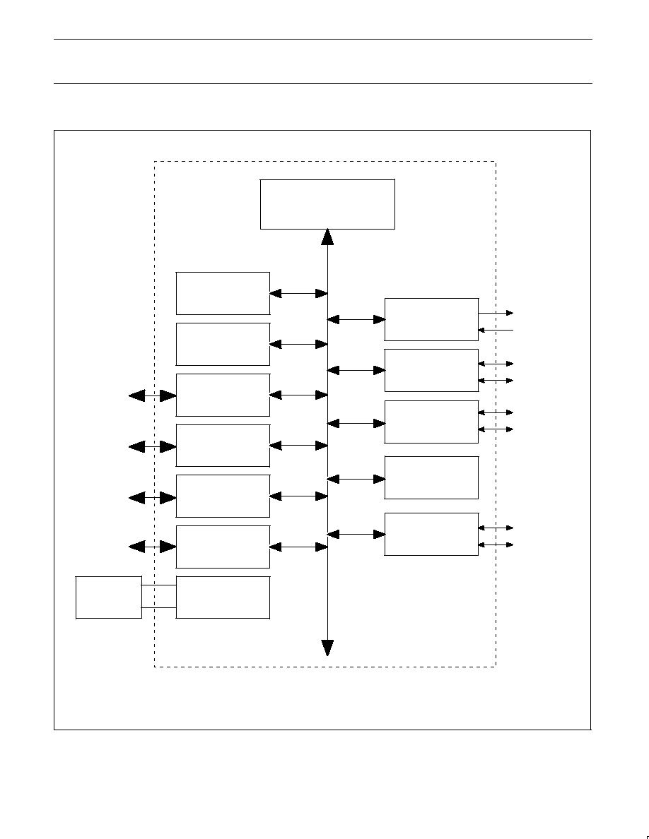
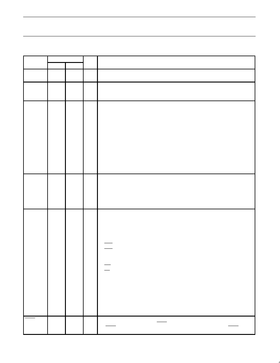
BLOCK DIAGRAM 1
su01728
ACCELERATED 80C51 CPU
(12-CLK MODE, 6-CLK MODE)
16 KB
CODE OTP/ROM
256 BYTE
DATA RAM
PORT 3
CONFIGURABLE I/Os
PORT 2
CONFIGURABLE I/Os
PORT 1
CONFIGURABLE I/Os
PORT 0
CONFIGURABLE I/Os
OSCILLATOR
CRYSTAL OR
RESONATOR
FULL-DUPLEX
ENHANCED UART
TIMER 0
TIMER 1
TIMER 2
WATCHDOG TIMER
FAST I
2
C
Philips Semiconductors
Product data
P83C654X2/P87C654X2
80C51 8-bit microcontroller family
16 kB OTP/ROM,
256B RAM, low voltage (2.7 to 5.5 V), low power, high speed
(30/33 MHz)
2004 Apr 20
4
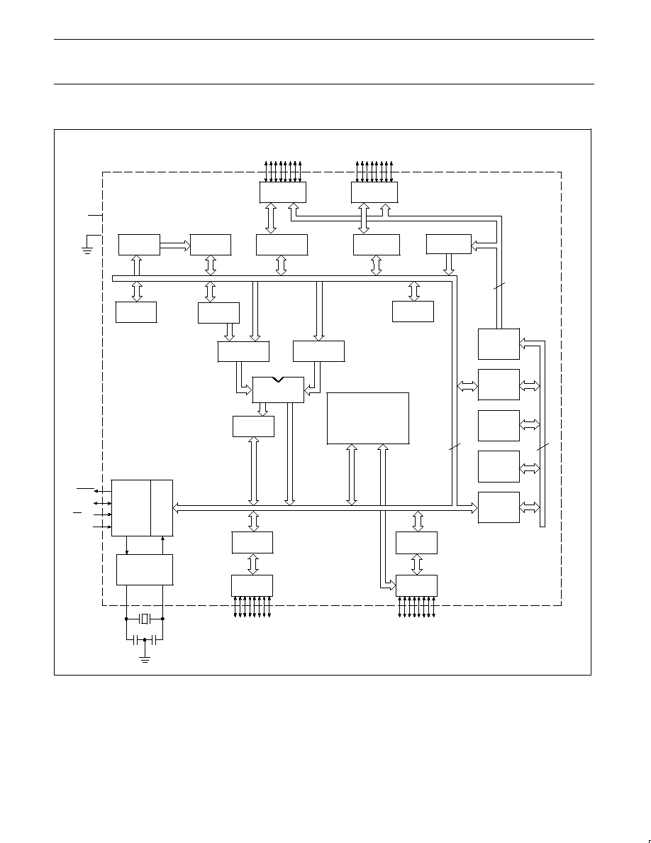
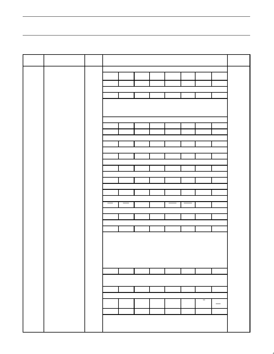
BLOCK DIAGRAM (CPU ORIENTED)
SU01751
PSEN
EAV
PP
ALE
RST
XTAL1
XTAL2
V
CC
V
SS
PORT 0
DRIVERS
PORT 2
DRIVERS
RAM ADDR
REGISTER
RAM
PORT 0
LATCH
PORT 2
LATCH
OTP/ROM
MEMORY
REGISTER
B
ACC
STACK
POINTER
TMP2
TMP1
ALU
TIMING
AND
CONTROL
INSTRUCTION
REGISTER
PD
OSCILLATOR
PSW
PORT 1
LATCH
PORT 3
LATCH
PORT 1
DRIVERS
PORT 3
DRIVERS
PROGRAM
ADDRESS
REGISTER
BUFFER
PC
INCRE-
MENTER
PROGRAM
COUNTER
DPTR'S
MULTIPLE
P1.0≠P1.7
P3.0≠P3.7
P0.0≠P0.7
P2.0≠P2.7
SFRs
TIMERS
P.C.A.
8
8
16

Philips Semiconductors
Product data
P83C654X2/P87C654X2
80C51 8-bit microcontroller family
16 kB OTP/ROM,
256B RAM, low voltage (2.7 to 5.5 V), low power, high speed
(30/33 MHz)
2004 Apr 20
5
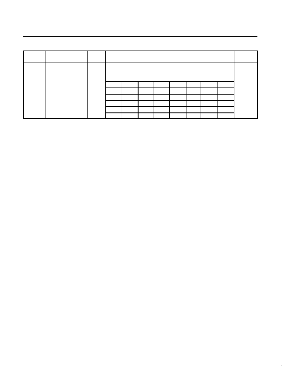
LOGIC SYMBOL
POR
T
0
POR
T
1
POR
T
2
POR
T
3
ADDRESS AND
DATA BUS
ADDRESS BUS
T2
T2EX
RxD
TxD
INT0
INT1
T0
T1
WR
RD
SECONDAR
Y
FUNCTIONS
RST
EA/V
PP
PSEN
ALE/PROG
V
SS
V
CC
XTAL1
XTAL2
SU01730
SCL0
SDA0
SCL1
SDA1
PINNING
Plastic Leaded Chip Carrier
LCC
6
1
40
7
17
39
29
18
28
Pin
Function
1
NIC
1
2
P1.0/T2
3
P1.1/T2EX
4
P1.2/ECI
5
P1.3
6
P1.4
7
P1.5
8
P1.6/SCL0
9
P1.7/SDA0
10
RST
11
P3.0/RxD
12
V
SS3
2
13
P3.1/TxD
14
P3.2/INT0
15
P3.3/INT1
Pin
Function
16
P3.4/T0
17
P3.5/T1
18
P3.6/WR
19
P3.7/RD
20
XTAL2
21
XTAL1
22
V
SS1
23
NIC
1
24
P2.0/A8
25
P2.1/A9
26
P2.2/A10
27
P2.3/A11
28
P2.4/A12
29
P2.5/A13
30
P2.6/A14
Pin
Function
31
P2.7/A15
32
PSEN
33
ALE
34
V
SS2
2
35
EA/V
PP
36
P0.7/AD7
37
P0.6/AD6
38
P0.5/AD5
39
P0.4/AD4
40
P0.3/AD3
41
P0.2/AD2
42
P0.1/AD1
43
P0.0/AD0
44
V
CC
SU01729
1. No internal connection
2. May be left open, but it is recommended that V
SS2
and V
SS3
be
connected to GND to improve EMC performance
Plastic Quad Flat Pack
LQFP
44
34
1
11
33
23
12
22
Pin
Function
1
P1.5
2
P1.6/SCL0
3
P1.7/SDA0
4
RST
5
P3.0/RxD
6
V
SS3
2
7
P3.1/TxD
8
P3.2/INT0
9
P3.3/INT1
10
P3.4/T0
11
P3.5/T1
12
P3.6/WR
13
P3.7/RD
14
XTAL2
15
XTAL1
Pin
Function
16
V
SS1
17
NIC
1
18
P2.0/A8
19
P2.1/A9
20
P2.2/A10
21
P2.3/A11
22
P2.4/A12
23
P2.5/A13
24
P2.6/A14
25
P2.7/A15
26
PSEN
27
ALE
28
V
SS2
2
29
EA/V
PP
30
P0.7/AD7
Pin
Function
31
P0.6/AD6
32
P0.5/AD5
33
P0.4/AD4
34
P0.3/AD3
35
P0.2/AD2
36
P0.1/AD1
37
P0.0/AD0
38
V
CC
39
NIC
1
40
P1.0/T2
41
P1.1/T2EX
42
P1.2/ECI
43
P1.3
44
P1.4
SU01731
1. No internal connection
2. May be left open, but it is recommended that V
SS2
and V
SS3
be
connected to GND to improve EMC performance
Philips Semiconductors
Product data
P83C654X2/P87C654X2
80C51 8-bit microcontroller family
16 kB OTP/ROM,
256B RAM, low voltage (2.7 to 5.5 V), low power, high speed
(30/33 MHz)
2004 Apr 20
6
PIN DESCRIPTIONS
MNEMONIC
PIN NUMBER
TYPE
NAME AND FUNCTION
MNEMONIC
PLCC
LQFP
TYPE
NAME AND FUNCTION
V
SS
22
16
I
Ground: 0 V reference.
V
CC
44
38
I
Power Supply: This is the power supply voltage for normal, idle, and power-down operation.
P0.0≠0.7
2
43≠36
37≠30
I/O
Port 0: Port 0 is an open-drain, bidirectional I/O port. Port 0 pins that have 1s written to them
float and can be used as high-impedance inputs. Port 0 is also the multiplexed low-order
address and data bus during accesses to external program and data memory. In this
application, it uses strong internal pull-ups when emitting 1s.
P1.0≠P1.7
2
2≠9
40≠44,
1≠3
I/O
Port 1: Port 1 is an 8-bit bidirectional I/O port with internal pull-ups on all pins. Port 1 pins that
have 1s written to them are pulled HIGH by the internal pull-ups and can be used as inputs. As
inputs, port 1 pins that are externally pulled LOW will source current because of the internal
pull-ups. (See DC Electrical Characteristics: I
IL
).
Alternate functions for P8xC654X2 Port 1 include:
2
40
I/O
T2 (P1.0): Timer/Counter 2 external count input/Clockout (see Programmable Clock-Out)
3
41
I
T2EX (P1.1): Timer/Counter 2 Reload/Capture/Direction Control
3
41
I
4
42
I
5
43
I/O
6
44
I/O
7
1
I/O
8
2
I/O
SCL (P1.6): I
2
C-bus clock line (open drain)
9
3
I/O
SDA (P1.7): I
2
C-bus data line (open drain)
P2.0≠P2.7
2
24≠31
18≠25
I/O
Port 2: Port 2 is an 8-bit bidirectional I/O port with internal pull-ups. Port 2 pins that have 1s
written to them are pulled HIGH by the internal pull-ups and can be used as inputs. As inputs,
port 2 pins that are externally being pulled LOW will source current because of the internal
pull-ups. (See DC Electrical Characteristics: I
IL
). Port 2 emits the high-order address byte
during fetches from external program memory and during accesses to external data memory
that use 16-bit addresses (MOVX @DPTR). In this application, it uses strong internal pull-ups
when emitting 1s. During accesses to external data memory that use 8-bit addresses (MOV
@Ri), port 2 emits the contents of the P2 special function register.
P3.0≠P3.7
2
11,
13≠19
5, 7≠13
I/O
Port 3: Port 3 is an 8-bit bidirectional I/O port with internal pull-ups. Port 3 pins that have 1s
written to them are pulled HIGH by the internal pull-ups and can be used as inputs. As inputs,
port 3 pins that are externally being pulled LOW will source current because of the pull-ups.
(See DC Electrical Characteristics: I
IL
). Port 3 also serves the special features of the
P8xC654X2, as listed below:
11
5
I
RxD (P3.0): Serial input port
13
7
O
TxD (P3.1): Serial output port
14
8
I
INT0 (P3.2): External interrupt 0
15
9
I
INT1 (P3.3): External interrupt 1
16
10
I
T0 (P3.4): Timer 0 external input
17
11
I
T1 (P3.5): Timer 1 external input
18
12
O
WR (P3.6): External data memory write strobe
19
13
O
RD (P3.7): External data memory read strobe
RST
2
10
4
I
Reset: A HIGH on this pin for two machine cycles while the oscillator is running, resets the
device. An internal diffused resistor to V
SS
permits a power-on reset using only an external
capacitor to V
CC
.
ALE
2
33
27
O
Address Latch Enable: Output pulse for latching the LOW byte of the address during an
access to external memory. In normal operation, ALE is emitted at constant rate of 1/6 the
oscillator frequency in 12x clock mode, 1/3 the oscillator frequency in 6x clock mode, and can
be used for external timing or clocking. Note that one ALE pulse is skipped during each access
to external data memory. ALE can be disabled by setting SFR auxiliary.0. With this bit set, ALE
will be active only during a MOVX instruction.
PSEN
2
32
26
O
Program Store Enable: The read strobe to external program memory. When executing code
from the external program memory, PSEN is activated twice each machine cycle, except that
two PSEN activations are skipped during each access to external data memory. PSEN is not
activated during fetches from internal program memory.

Philips Semiconductors
Product data
P83C654X2/P87C654X2
80C51 8-bit microcontroller family
16 kB OTP/ROM,
256B RAM, low voltage (2.7 to 5.5 V), low power, high speed
(30/33 MHz)
2004 Apr 20
7
MNEMONIC
NAME AND FUNCTION
TYPE
PIN NUMBER
MNEMONIC
NAME AND FUNCTION
TYPE
LQFP
PLCC
EA
2
35
29
I
External Access Enable/Programming Supply Voltage: EA must be externally held LOW to
enable the device to fetch code from external program memory. The value on the EA pin is
latched when RST is released and any subsequent changes have no effect.
XTAL1
21
15
I
Crystal 1: Input to the inverting oscillator amplifier and input to the internal clock generator
circuits.
XTAL2
20
14
O
Crystal 2: Output from the inverting oscillator amplifier.
NOTES:
1. To avoid "latch-up" effect at power-on, the voltage on any pin (other than EA) at any time must not be higher than V
CC
+ 0.5 V or less than
V
SS
≠ 0.5 V, respectively.
2. The pins are designed for test mode also.
Philips Semiconductors
Product data
P83C654X2/P87C654X2
80C51 8-bit microcontroller family
16 kB OTP/ROM,
256B RAM, low voltage (2.7 to 5.5 V), low power, high speed
(30/33 MHz)
2004 Apr 20
8
SPECIAL FUNCTION REGISTERS
SYMBOL
DESCRIPTION
DIRECT
ADDRESS
BIT ADDRESS, SYMBOL, OR ALTERNATIVE PORT FUNCTION
MSB
LSB
RESET
VALUE
ACC*
Accumulator
E0H
E7
E6
E5
E4
E3
E2
E1
E0
00H
AUXR#
Auxiliary
8EH
≠
≠
≠
≠
Fast/STD
I
2
C
≠
≠
AO
xxxx1xx0B
AUXR1#
Auxiliary 1
A2H
≠
≠
≠
LPEP
GPS
0
≠
DPS
xxxx00x0B
B*
B register
F0H
F7
F6
F5
F4
F3
F2
F1
F0
00H
CKCON
Clock control
8FH
≠
≠
≠
≠
≠
≠
≠
X2
xxxxxxx0B
DPTR:
Data Pointer (2 bytes)
DPH
Data Pointer High
83H
00H
DPL
Data Pointer Low
82H
00H
AF
AE
AD
AC
AB
AA
A9
A8
IEN0*
Interrupt Enable 0
A8H
EA
EC
ES1
ES0
ET1
EX1
ET0
EX0
00000000B
IEN1*
Interrupt Enable 1
E8H
≠
≠
≠
≠
≠
≠
ES2
ET2
xxxxxx00B
BF
BE
BD
BC
BB
BA
B9
B8
IP*#
Interrupt Priority
B8H
PT2
≠
PS1
PS0
PT1
PX1
PT0
PX0
00000000B
B7
B6
B5
B4
B3
B2
B1
B0
IPH#
Interrupt Priority High
B7H
PT2H
PPCH
PS1H
PS0H
PT1H
PX1H
PT0H
PX0H
00000000B
87
86
85
84
83
82
81
80
P0*
Port 0
80H
AD7
AD6
AD5
AD4
AD3
AD2
AD1
AD0
FFH
97
96
95
94
93
92
91
90
P1*#
Port 1
90H
SDA
SCL
≠
≠
≠
≠
T2EX
T2
FFH
A7
A6
A5
A4
A3
A2
A1
A0
P2*
Port 2
A0H
AD15
AD14
AD13
AD12
AD11
AD10
AD9
AD8
FFH
B7
B6
B5
B4
B3
B2
B1
B0
P3*
Port 3
B0H
RD
WR
T1
T0
INT1
INT0
TxD
RxD
FFH
PCON#
1
Power Control
87H
SMOD1
SMOD0
≠
POF
GF1
GF0
PD
IDL
00xx0000B
D7
D6
D5
D4
D3
D2
D1
D0
PSW*
Program Status Word
D0H
CY
AC
F0
RS1
RS0
OV
F1
P
00000000B
RCAP2H
#
Timer 2 Capture High
CBH
00H
RCAP2L
#
Timer 2 Capture Low
CAH
00H
SADDR#
Slave Address
A9H
00H
SADEN#
Slave Address Mask
B9H
00H
SBUF
Serial Data Buffer
99H
xxxxxxxxB
9F
9E
9D
9C
9B
9A
99
98
SCON*
Serial Control
98H
SM0/FE
SM1
SM2
REN
TB8
RB8
TI
RI
00H
SP
Stack Pointer
81H
07H
8F
8E
8D
8C
8B
8A
89
88
TCON*
Timer Control
88H
TF1
TR1
TF0
TR0
IE1
IT1
IE0
IT0
00H
CF
CE
CD
CC
CB
CA
C9
C8
T2CON*
Timer 2 Control
C8H
TF2
EXF2
RCLK
TCLK
EXEN2
TR2
C/T2
CP/
RL2
00H
T2MOD#
Timer 2 Mode Control
C9H
≠
≠
≠
≠
≠
≠
T2OE
DCEN
xxxxxx00B
TH0
Timer High 0
8CH
00H
TH1
Timer High 1
8DH
00H
TH2#
Timer High 2
CDH
00H
Philips Semiconductors
Product data
P83C654X2/P87C654X2
80C51 8-bit microcontroller family
16 kB OTP/ROM,
256B RAM, low voltage (2.7 to 5.5 V), low power, high speed
(30/33 MHz)
2004 Apr 20
9
SYMBOL
RESET
VALUE
BIT ADDRESS, SYMBOL, OR ALTERNATIVE PORT FUNCTION
MSB
LSB
DIRECT
ADDRESS
DESCRIPTION
TL0
Timer Low 0
8AH
00H
TL1
Timer Low 1
8BH
00H
TL2#
Timer Low 2
CCH
00H
TMOD
Timer Mode
89H
GATE
C/T
M1
M0
GATE
C/T
M1
M0
00H
S1CON
I2C Control
D8H
CR2
ENA1
STA
STO
SI
AA
CR1
CR0
00H
S1STA
I2C STATUS
D9H
SC4
SC3
SC2
SC1
SC0
0
0
0
F8H
S1DAT
I2C DATA
DAH
00H
S1ADR
I2C ADDRESS
DBH
GC
00H
WDTRST
Watchdog Reset Timer
A6H
*
SFRs are bit addressable.
#
SFRs are modified from or added to the 80C51 SFRs.
≠
Reserved bits.
1. Reset value depends on reset source.
Philips Semiconductors
Product data
P83C654X2/P87C654X2
80C51 8-bit microcontroller family
16 kB OTP/ROM,
256B RAM, low voltage (2.7 to 5.5 V), low power, high speed
(30/33 MHz)
2004 Apr 20
10
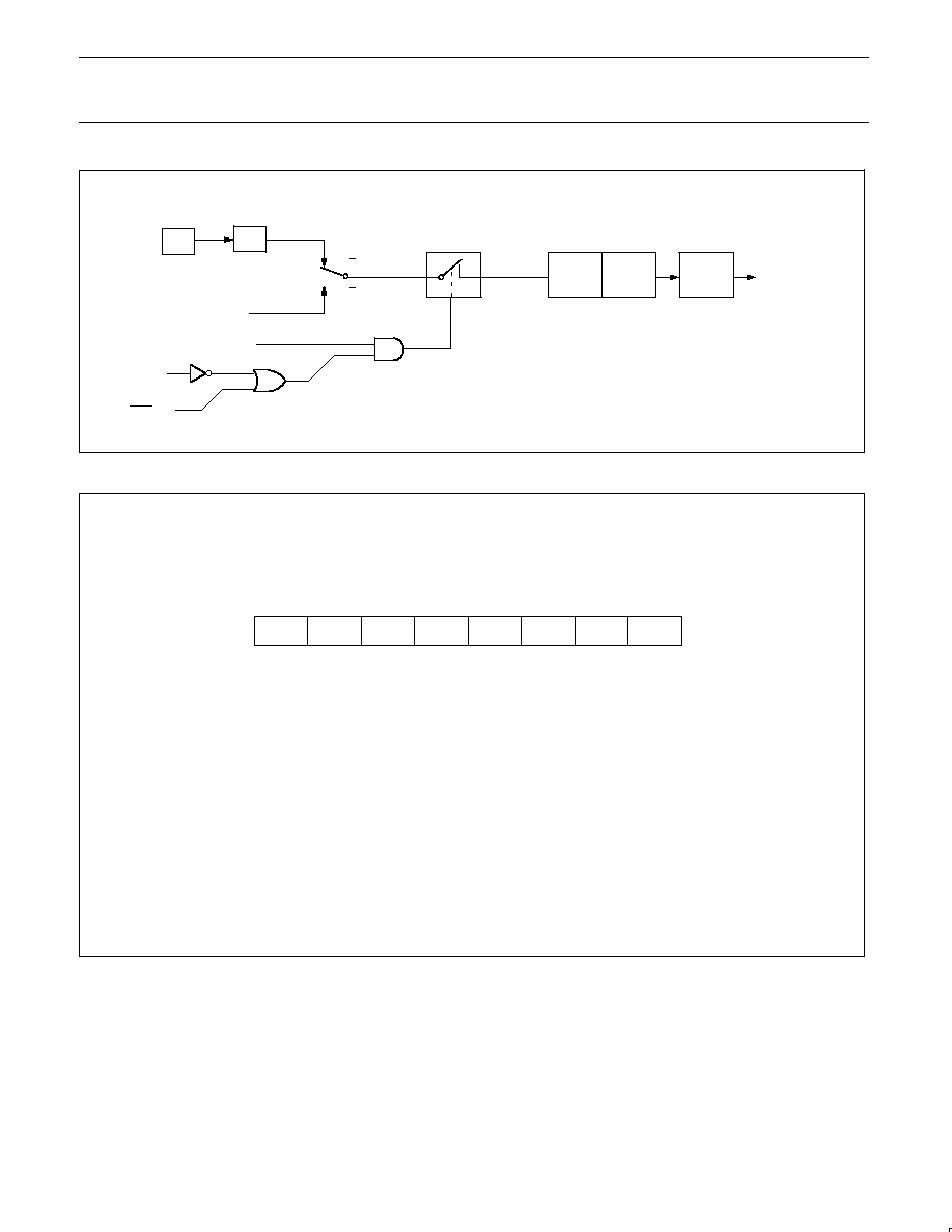
CLOCK CONTROL REGISTER (CKCON)
This device allows control of the 6-clock/12-clock mode by means of
both an SFR bit (X2) and an OTP bit. The OTP clock control bit
OX2, when programmed (6-clock mode), supersedes the X2 bit
(CKCON.0). The CKCON register is shown below in Figure 1.
X2
BIT
SYMBOL
FUNCTION
CKCON.7
≠
Reserved.
CKCON.6
Reserved.
CKCON.5
Reserved.
CKCON.4
Reserved.
CKCON.3
Reserved.
CKCON.2
Reserved.
CKCON.1
Reserved.
CKCON.0
X2
CPU clock; 1 = 6 clocks for each machine cycle, 0 = 12 clocks for each machine cycle
SU01689
≠
≠
Not Bit Addressable
CKCON
Address = 8Fh
Reset Value =
x0000000B
7
6
5
4
3
2
1
0
≠
≠
≠
≠
≠
Figure 1. Clock control (CKCON) register
Also please note that the clock divider applies to the serial port for
modes 0 and 2 (fixed baud rate modes). This is because modes 1
and 3 (variable baud rate modes) use either Timer 1 or Timer 2.
Below is the truth table for the CPU clock mode.
Table 1.
OX2 clock mode bit
(can only be set by
parallel programmer)
X2 bit
(CKCON.0)
CPU clock mode
erased
0
12-clock mode
(default)
erased
1
6-clock mode
programmed
X
6-clock mode

Philips Semiconductors
Product data
P83C654X2/P87C654X2
80C51 8-bit microcontroller family
16 kB OTP/ROM,
256B RAM, low voltage (2.7 to 5.5 V), low power, high speed
(30/33 MHz)
2004 Apr 20
11
OSCILLATOR CHARACTERISTICS
XTAL1 and XTAL2 are the input and output, respectively, of an
inverting amplifier. The pins can be configured for use as an
on-chip oscillator.
To drive the device from an external clock source, XTAL1 should be
driven while XTAL2 is left unconnected. Minimum and maximum
high and low times specified in the data sheet must be observed.
This device is configured at the factory to operate using 12 clock
periods per machine cycle, referred to in this datasheet as "12-clock
mode". It may be optionally configured on commercially available
EPROM programming equipment to operate at 6 clocks per machine
cycle, referred to in this datasheet as "6-clock mode". (This yields
performance equivalent to twice that of standard 80C51 family
devices). Also see next page.
RESET
A reset is accomplished by holding the RST pin HIGH for at least
two machine cycles (12 oscillator periods in 6-clock mode, or 24
oscillator periods in 12-clock mode), while the oscillator is running.
To insure a good power-on reset, the RST pin must be HIGH long
enough to allow the oscillator time to start up (normally a few
milliseconds) plus two machine cycles. At power-on, the voltage on
V
CC
and RST must come up at the same time for a proper start-up.
Ports 1, 2, and 3 will asynchronously be driven to their reset
condition when a voltage above V
IH (min.)
is applied to RESET. The
value on the EA pin is latched when RST is deasserted and has no
further effect.
LOW POWER MODES
Stop Clock Mode
The static design enables the clock speed to be reduced down to
0 MHz (stopped). When the oscillator is stopped, the RAM and
Special Function Registers retain their values. This mode allows
step-by-step utilization and permits reduced system power
consumption by lowering the clock frequency down to any value. For
lowest power consumption the Power-down mode is suggested.
Idle Mode
In the idle mode (see Table 2), the CPU puts itself to sleep while all
of the on-chip peripherals stay active. The instruction to invoke the
idle mode is the last instruction executed in the normal operating
mode before the idle mode is activated. The CPU contents, the
on-chip RAM, and all of the special function registers remain intact
during this mode. The idle mode can be terminated either by any
enabled interrupt (at which time the process is picked up at the
interrupt service routine and continued), or by a hardware reset
which starts the processor in the same manner as a power-on reset.
Power-Down Mode
To save even more power, a Power-down mode (see Table 2) can
be invoked by software. In this mode, the oscillator is stopped and
the instruction that invoked power-down is the last instruction
executed. The on-chip RAM and Special Function Registers retain
their values down to 2 V and care must be taken to return V
CC
to the
minimum specified operating voltages before the Power-down mode
is terminated.
Either a hardware reset or external interrupt can be used to exit from
power-down. Reset redefines all the SFRs but does not change the
on-chip RAM. An external interrupt allows both the SFRs and the
on-chip RAM to retain their values.
To properly terminate power-down, the reset or external interrupt
should not be executed before V
CC
is restored to its normal
operating level and must be held active long enough for the
oscillator to restart and stabilize (normally less than 10 ms).
With an external interrupt, INT0 and INT1 must be enabled and
configured as level-sensitive. Holding the pin LOW restarts the
oscillator but bringing the pin back HIGH completes the exit. Once
the interrupt is serviced, the next instruction to be executed after
RETI will be the one following the instruction that put the device into
power-down.
POWER-OFF FLAG
The Power-Off Flag (POF) is set by on-chip circuitry when the V
CC
level on the P8xC654X2 rises from 0 to 5 V. The POF bit can be set
or cleared by software allowing a user to determine if the reset is the
result of a power-on or a warm start after power-down. The V
CC
level must remain above 3 V for the POF to remain unaffected by
the V
CC
level.
Low-Power EPROM operation (LPEP)
The EPROM array contains some analog circuits that are not
required when V
CC
is less than 4 V, but are required for a V
CC
greater than 4 V. The LPEP bit (AUXR.4), when set, will power-down
these analog circuits resulting in a reduced supply current. This bit
should be set ONLY for applications that operate at a V
CC
less than
4 V.
Design Consideration
When the idle mode is terminated by a hardware reset, the device
normally resumes program execution, from where it left off, up to
two machine cycles before the internal reset algorithm takes control.
On-chip hardware inhibits access to internal RAM in this event, but
access to the port pins is not inhibited. To eliminate the possibility of
an unexpected write when Idle is terminated by reset, the instruction
following the one that invokes Idle should not be one that writes to a
port pin or to external memory.
ONCE
TM
Mode
The ONCE ("On-Circuit Emulation") Mode facilitates testing and
debugging of systems without the device having to be removed from
the circuit. The ONCE Mode is invoked by:
1. Pull ALE LOW while the device is in reset and PSEN is HIGH;
2. Hold ALE LOW as RST is deactivated.
While the device is in ONCE Mode, the Port 0 pins go into a float
state, and the other port pins and ALE and PSEN are weakly pulled
HIGH. The oscillator circuit remains active. While the device is in
this mode, an emulator or test CPU can be used to drive the circuit.
Normal operation is restored when a normal reset is applied.
Programmable Clock-Out
A 50 % duty cycle clock can be programmed to come out on P1.0.
This pin, besides being a regular I/O pin, has two alternate
functions. It can be programmed:
1. to input the external clock for Timer/Counter 2, or
2. to output a 50 % duty cycle clock ranging from 122 Hz to 8 MHz at
a 16 MHz operating frequency (61 Hz to 4 MHz in 12-clock mode).
To configure the Timer/Counter 2 as a clock generator, bit C/T2 (in
T2CON) must be cleared and bit T20E in T2MOD must be set. Bit
TR2 (T2CON.2) also must be set to start the timer.

Philips Semiconductors
Product data
P83C654X2/P87C654X2
80C51 8-bit microcontroller family
16 kB OTP/ROM,
256B RAM, low voltage (2.7 to 5.5 V), low power, high speed
(30/33 MHz)
2004 Apr 20
12
The Clock-Out frequency depends on the oscillator frequency and
the reload value of Timer 2 capture registers (RCAP2H, RCAP2L)
as shown in this equation:
Oscillator Frequency
n
(65536
*
RCAP2H, RCAP2L)
n =
2 in 6-clock mode
4 in 12-clock mode
Where (RCAP2H,RCAP2L) = the content of RCAP2H and RCAP2L
taken as a 16-bit unsigned integer.
In the Clock-Out mode Timer 2 roll-overs will not generate an
interrupt. This is similar to when it is used as a baud-rate generator.
It is possible to use Timer 2 as a baud-rate generator and a clock
generator simultaneously. Note, however, that the baud-rate and the
Clock-Out frequency will be the same.
Table 2.
External Pin Status During Idle and Power-Down Mode
MODE
PROGRAM MEMORY
ALE
PSEN
PORT 0
PORT 1
PORT 2
PORT 3
Idle
Internal
1
1
Data
Data
Data
Data
Idle
External
1
1
Float
Data
Address
Data
Power-down
Internal
0
0
Data
Data
Data
Data
Power-down
External
0
0
Float
Data
Data
Data

Philips Semiconductors
Product data
P83C654X2/P87C654X2
80C51 8-bit microcontroller family
16 kB OTP/ROM,
256B RAM, low voltage (2.7 to 5.5 V), low power, high speed
(30/33 MHz)
2004 Apr 20
13
TIMER 0 AND TIMER 1 OPERATION
Timer 0 and Timer 1
The "Timer" or "Counter" function is selected by control bits C/T in
the Special Function Register TMOD. These two Timer/Counters
have four operating modes, which are selected by bit-pairs (M1, M0)
in TMOD. Modes 0, 1, and 2 are the same for both Timers/Counters.
Mode 3 is different. The four operating modes are described in the
following text.
Mode 0
Putting either Timer into Mode 0 makes it look like an 8048 Timer,
which is an 8-bit Counter with a divide-by-32 prescaler. Figure 3
shows the Mode 0 operation.
In this mode, the Timer register is configured as a 13-bit register. As
the count rolls over from all 1s to all 0s, it sets the Timer interrupt
flag TFn. The counted input is enabled to the Timer when TRn = 1
and either GATE = 0 or INTn = 1. (Setting GATE = 1 allows the
Timer to be controlled by external input INTn, to facilitate pulse width
measurements). TRn is a control bit in the Special Function Register
TCON (Figure 4).
The 13-bit register consists of all 8 bits of THn and the lower 5 bits
of TLn. The upper 3 bits of TLn are indeterminate and should be
ignored. Setting the run flag (TRn) does not clear the registers.
Mode 0 operation is the same for Timer 0 as for Timer 1. There are
two different GATE bits, one for Timer 1 (TMOD.7) and one for Timer
0 (TMOD.3).
Mode 1
Mode 1 is the same as Mode 0, except that the Timer register is
being run with all 16 bits.
Mode 2
Mode 2 configures the Timer register as an 8-bit Counter (TLn) with
automatic reload, as shown in Figure 5. Overflow from TLn not only
sets TFn, but also reloads TLn with the contents of THn, which is
preset by software. The reload leaves THn unchanged.
Mode 2 operation is the same for Timer 0 as for Timer 1.
Mode 3
Timer 1 in Mode 3 simply holds its count. The effect is the same as
setting TR1 = 0.
Timer 0 in Mode 3 establishes TL0 and TH0 as two separate
counters. The logic for Mode 3 on Timer 0 is shown in Figure 6. TL0
uses the Timer 0 control bits: C/T, GATE, TR0, and TF0 as well as
pin INT0. TH0 is locked into a timer function (counting machine
cycles) and takes over the use of TR1 and TF1 from Timer 1. Thus,
TH0 now controls the "Timer 1" interrupt.
Mode 3 is provided for applications requiring an extra 8-bit timer on
the counter. With Timer 0 in Mode 3, an 80C51 can look like it has
three Timer/Counters. When Timer 0 is in Mode 3, Timer 1 can be
turned on and off by switching it out of and into its own Mode 3, or
can still be used by the serial port as a baud rate generator, or in
fact, in any application not requiring an interrupt.
GATE
C/T
M1
M0
GATE
C/T
M1
M0
BIT
SYMBOL
FUNCTION
TMOD.3/
GATE
Gating control when set. Timer/Counter "n" is enabled only while "INTn" pin is high and
TMOD.7
"TRn" control pin is set. when cleared Timer "n" is enabled whenever "TRn" control bit is set.
TMOD.2/
C/T
Timer or Counter Selector cleared for Timer operation (input from internal system clock.)
TMOD.6
Set for Counter operation (input from "Tn" input pin).
M1
M0
OPERATING
0
0
8048 Timer: "TLn" serves as 5-bit prescaler.
0
1
16-bit Timer/Counter: "THn" and "TLn" are cascaded; there is no prescaler.
1
0
8-bit auto-reload Timer/Counter: "THn" holds a value which is to be reloaded
into "TLn" each time it overflows.
1
1
(Timer 0) TL0 is an 8-bit Timer/Counter controlled by the standard Timer 0 control bits.
TH0 is an 8-bit timer only controlled by Timer 1 control bits.
1
1
(Timer 1) Timer/Counter 1 stopped.
SU01580
TIMER 1
TIMER 0
Not Bit Addressable
TMOD
Address = 89H
Reset Value = 00H
7
6
5
4
3
2
1
0
Figure 2. Timer/Counter 0/1 Mode Control (TMOD) Register
Philips Semiconductors
Product data
P83C654X2/P87C654X2
80C51 8-bit microcontroller family
16 kB OTP/ROM,
256B RAM, low voltage (2.7 to 5.5 V), low power, high speed
(30/33 MHz)
2004 Apr 20
14
INTn Pin
Timer n
Gate bit
TRn
TLn
(5 Bits)
THn
(8 Bits)
TFn
Interrupt
Control
C/T = 0
C/T = 1
SU01618
OSC
˜
d*
Tn Pin
*d = 6 in 6-clock mode; d = 12 in 12-clock mode.
Figure 3. Timer/Counter 0/1 Mode 0: 13-Bit Timer/Counter
IT0
BIT
SYMBOL
FUNCTION
TCON.7
TF1
Timer 1 overflow flag. Set by hardware on Timer/Counter overflow.
Cleared by hardware when processor vectors to interrupt routine, or clearing the bit in software.
TCON.6
TR1
Timer 1 Run control bit. Set/cleared by software to turn Timer/Counter on/off.
TCON.5
TF0
Timer 0 overflow flag. Set by hardware on Timer/Counter overflow.
Cleared by hardware when processor vectors to interrupt routine, or by clearing the bit in software.
TCON.4
TR0
Timer 0 Run control bit. Set/cleared by software to turn Timer/Counter on/off.
TCON.3
IE1
Interrupt 1 Edge flag. Set by hardware when external interrupt edge detected.
Cleared when interrupt processed.
TCON.2
IT1
Interrupt 1 type control bit. Set/cleared by software to specify falling edge/low level triggered
external interrupts.
TCON.1
IE0
Interrupt 0 Edge flag. Set by hardware when external interrupt edge detected.
Cleared when interrupt processed.
TCON.0
IT0
Interrupt 0 Type control bit. Set/cleared by software to specify falling edge/low level
triggered external interrupts.
SU01516
IE0
IT1
IE1
TR0
TF0
TR1
TF1
Bit Addressable
TCON
Address = 88H
Reset Value = 00H
7
6
5
4
3
2
1
0
Figure 4. Timer/Counter 0/1 Control (TCON) Register

Philips Semiconductors
Product data
P83C654X2/P87C654X2
80C51 8-bit microcontroller family
16 kB OTP/ROM,
256B RAM, low voltage (2.7 to 5.5 V), low power, high speed
(30/33 MHz)
2004 Apr 20
15
TLn
(8 Bits)
TFn
Interrupt
Control
C/T = 0
C/T = 1
THn
(8 Bits)
Reload
INTn Pin
Timer n
Gate bit
TRn
SU01619
OSC
˜
d*
Tn Pin
*d = 6 in 6-clock mode; d = 12 in 12-clock mode.
Figure 5. Timer/Counter 0/1 Mode 2: 8-Bit Auto-Reload
TL0
(8 Bits)
TF0
Interrupt
Control
TH0
(8 Bits)
TF1
Interrupt
Control
TR1
INT0 Pin
Timer 0
Gate bit
TR0
SU01620
C/T = 0
C/T = 1
*d = 6 in 6-clock mode; d = 12 in 12-clock mode.
OSC
˜
d*
OSC
˜
d*
T0 Pin
Figure 6. Timer/Counter 0 Mode 3: Two 8-Bit Counters
Philips Semiconductors
Product data
P83C654X2/P87C654X2
80C51 8-bit microcontroller family
16 kB OTP/ROM,
256B RAM, low voltage (2.7 to 5.5 V), low power, high speed
(30/33 MHz)
2004 Apr 20
16
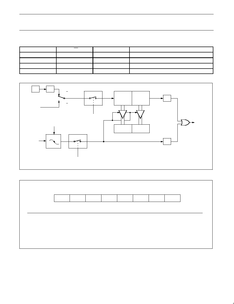
TIMER 2 OPERATION
Timer 2
Timer 2 is a 16-bit Timer/Counter which can operate as either an
event timer or an event counter, as selected by C/T2 in the special
function register T2CON (see Figure 7). Timer 2 has three operating
modes: Capture, Auto-reload (up or down counting), and Baud Rate
Generator, which are selected by bits in the T2CON as shown in
Table 3.
Capture Mode
In the capture mode there are two options which are selected by bit
EXEN2 in T2CON. If EXEN2 = 0, then timer 2 is a 16-bit timer or
counter (as selected by C/T2 in T2CON) which, upon overflowing
sets bit TF2, the timer 2 overflow bit. This bit can be used to
generate an interrupt (by enabling the Timer 2 interrupt bit in the
IE register). If EXEN2 = 1, Timer 2 operates as described above, but
with the added feature that a 1- to -0 transition at external input
T2EX causes the current value in the Timer 2 registers, TL2 and
TH2, to be captured into registers RCAP2L and RCAP2H,
respectively. In addition, the transition at T2EX causes bit EXF2 in
T2CON to be set, and EXF2 like TF2 can generate an interrupt
(which vectors to the same location as Timer 2 overflow interrupt.
The Timer 2 interrupt service routine can interrogate TF2 and EXF2
to determine which event caused the interrupt). The capture mode is
illustrated in Figure 8 (There is no reload value for TL2 and TH2 in
this mode. Even when a capture event occurs from T2EX, the
counter keeps on counting T2EX pin transitions or osc/6 pulses
(osc/12 in 12-clock mode).).
Auto-Reload Mode (Up or Down Counter)
In the 16-bit auto-reload mode, Timer 2 can be configured (as either
a timer or counter [C/T2 in T2CON]) then programmed to count up
or down. The counting direction is determined by bit DCEN (Down
Counter Enable) which is located in the T2MOD register (see
Figure 9). When reset is applied the DCEN = 0 which means Timer
2 will default to counting up. If DCEN bit is set, Timer 2 can count up
or down depending on the value of the T2EX pin.
Figure 10 shows Timer 2 which will count up automatically since
DCEN = 0. In this mode there are two options selected by bit
EXEN2 in T2CON register. If EXEN2 = 0, then Timer 2 counts up to
0FFFFH and sets the TF2 (Overflow Flag) bit upon overflow. This
causes the Timer 2 registers to be reloaded with the 16-bit value in
RCAP2L and RCAP2H. The values in RCAP2L and RCAP2H are
preset by software means.
If EXEN2 = 1, then a 16-bit reload can be triggered either by an
overflow or by a 1-to-0 transition at input T2EX. This transition also
sets the EXF2 bit. The Timer 2 interrupt, if enabled, can be
generated when either TF2 or EXF2 are 1.
In Figure 11 DCEN = 1 which enables Timer 2 to count up or down.
This mode allows pin T2EX to control the direction of count. When a
logic 1 is applied at pin T2EX Timer 2 will count up. Timer 2 will
overflow at 0FFFFH and set the TF2 flag, which can then generate
an interrupt, if the interrupt is enabled. This timer overflow also
causes the 16-bit value in RCAP2L and RCAP2H to be reloaded
into the timer registers TL2 and TH2.
When a logic 0 is applied at pin T2EX this causes Timer 2 to count
down. The timer will underflow when TL2 and TH2 become equal to
the value stored in RCAP2L and RCAP2H. Timer 2 underflow sets
the TF2 flag and causes 0FFFFH to be reloaded into the timer
registers TL2 and TH2.
The external flag EXF2 toggles when Timer 2 underflows or overflows.
This EXF2 bit can be used as a 17th bit of resolution if needed. The
EXF2 flag does not generate an interrupt in this mode of operation.
(MSB)
(LSB)
Symbol
Position
Name and Significance
TF2
T2CON.7
Timer 2 overflow flag set by a Timer 2 overflow and must be cleared by software. TF2 will not be set
when either RCLK or TCLK = 1.
EXF2
T2CON.6
Timer 2 external flag set when either a capture or reload is caused by a negative transition on T2EX and
EXEN2 = 1. When Timer 2 interrupt is enabled, EXF2 = 1 will cause the CPU to vector to the Timer 2
interrupt routine. EXF2 must be cleared by software. EXF2 does not cause an interrupt in up/down
counter mode (DCEN = 1).
RCLK
T2CON.5
Receive clock flag. When set, causes the serial port to use Timer 2 overflow pulses for its receive clock
in modes 1 and 3. RCLK = 0 causes Timer 1 overflow to be used for the receive clock.
TCLK
T2CON.4
Transmit clock flag. When set, causes the serial port to use Timer 2 overflow pulses for its transmit clock
in modes 1 and 3. TCLK = 0 causes Timer 1 overflows to be used for the transmit clock.
EXEN2
T2CON.3
Timer 2 external enable flag. When set, allows a capture or reload to occur as a result of a negative
transition on T2EX if Timer 2 is not being used to clock the serial port. EXEN2 = 0 causes Timer 2 to
ignore events at T2EX.
TR2
T2CON.2
Start/stop control for Timer 2. A logic 1 starts the timer.
C/T2
T2CON.1
Timer or counter select. (Timer 2)
0 = Internal timer (OSC/6 in 6-clock mode or OSC/12 in 12-clock mode)
1 = External event counter (falling edge triggered).
CP/RL2
T2CON.0
Capture/Reload flag. When set, captures will occur on negative transitions at T2EX if EXEN2 = 1. When
cleared, auto-reloads will occur either with Timer 2 overflows or negative transitions at T2EX when
EXEN2 = 1. When either RCLK = 1 or TCLK = 1, this bit is ignored and the timer is forced to auto-reload
on Timer 2 overflow.
TF2
EXF2
RCLK
TCLK
EXEN2
TR2
C/T2
CP/RL2
SU01251
Figure 7. Timer/Counter 2 (T2CON) Control Register
Philips Semiconductors
Product data
P83C654X2/P87C654X2
80C51 8-bit microcontroller family
16 kB OTP/ROM,
256B RAM, low voltage (2.7 to 5.5 V), low power, high speed
(30/33 MHz)
2004 Apr 20
17
Table 3.
Timer 2 Operating Modes
RCLK + TCLK
CP/RL2
TR2
MODE
0
0
1
16-bit Auto-reload
0
1
1
16-bit Capture
1
X
1
Baud rate generator
X
X
0
(off)
OSC
˜
n*
C/T2 = 0
C/T2 = 1
TR2
Control
TL2
(8 BITS)
TH2
(8 BITS)
TF2
RCAP2L
RCAP2H
EXEN2
Control
EXF2
Timer 2
Interrupt
T2EX Pin
Transition
Detector
T2 Pin
Capture
SU01252
* n = 6 in 6-clock mode, or 12 in 12-clock mode.
Figure 8. Timer 2 in Capture Mode
Not Bit Addressable
Symbol
Function
--
Not implemented, reserved for future use.*
T2OE
Timer 2 Output Enable bit.
DCEN
Down Count Enable bit. When set, this allows Timer 2 to be configured as an up/down counter.
--
--
--
--
--
--
T2OE
DCEN
SU00729
7
6
5
4
3
2
1
0
*
User software should not write 1s to reserved bits. These bits may be used in future 8051 family products to invoke new features.
In that case, the reset or inactive value of the new bit will be 0, and its active value will be 1. The value read from a reserved bit is
indeterminate.
Bit
T2MOD
Address = 0C9H
Reset Value = XXXX XX00B
Figure 9. Timer 2 Mode (T2MOD) Control Register

Philips Semiconductors
Product data
P83C654X2/P87C654X2
80C51 8-bit microcontroller family
16 kB OTP/ROM,
256B RAM, low voltage (2.7 to 5.5 V), low power, high speed
(30/33 MHz)
2004 Apr 20
18
OSC
˜
n*
C/T2 = 0
C/T2 = 1
TR2
CONTROL
TL2
(8 BITS)
TH2
(8 BITS)
TF2
RCAP2L
RCAP2H
EXEN2
CONTROL
EXF2
TIMER 2
INTERRUPT
T2EX PIN
TRANSITION
DETECTOR
T2 PIN
RELOAD
SU01253
* n = 6 in 6-clock mode, or 12 in 12-clock mode.
Figure 10. Timer 2 in Auto-Reload Mode (DCEN = 0)
˜
n*
C/T2 = 0
C/T2 = 1
TL2
TH2
TR2
CONTROL
T2 PIN
SU01254
FFH
FFH
RCAP2L
RCAP2H
(UP COUNTING RELOAD VALUE)
T2EX PIN
TF2
INTERRUPT
COUNT
DIRECTION
1 = UP
0 = DOWN
EXF2
OVERFLOW
(DOWN COUNTING RELOAD VALUE)
TOGGLE
OSC
* n = 6 in 6-clock mode, or 12 in 12-clock mode.
Figure 11. Timer 2 Auto Reload Mode (DCEN = 1)

Philips Semiconductors
Product data
P83C654X2/P87C654X2
80C51 8-bit microcontroller family
16 kB OTP/ROM,
256B RAM, low voltage (2.7 to 5.5 V), low power, high speed
(30/33 MHz)
2004 Apr 20
19
C/T2 = 0
C/T2 = 1
TR2
Control
TL2
(8-bits)
TH2
(8-bits)
˜
16
RCAP2L
RCAP2H
EXEN2
Control
EXF2
Timer 2
Interrupt
T2EX Pin
Transition
Detector
Reload
˜
2
"0"
"1"
RX Clock
˜
16
TX Clock
"0"
"1"
"0"
"1"
Timer 1
Overflow
Note availability of additional external interrupt.
SMOD
RCLK
TCLK
SU01629
n = 1 in 6-clock mode
n = 2 in 12-clock mode
OSC
˜
n
T2 Pin
Figure 12. Timer 2 in Baud Rate Generator Mode
Table 4.
Timer 2 Generated Commonly Used
Baud Rates
Baud Rate
Timer 2
12-clock
mode
6-clock
mode
Osc Freq
RCAP2H
RCAP2L
375 k
750 k
12 MHz
FF
FF
9.6 k
19.2 k
12 MHz
FF
D9
4.8 k
9.6 k
12 MHz
FF
B2
2.4 k
4.8 k
12 MHz
FF
64
1.2 k
2.4 k
12 MHz
FE
C8
300
600
12 MHz
FB
1E
110
220
12 MHz
F2
AF
300
600
6 MHz
FD
8F
110
220
6 MHz
F9
57
Baud Rate Generator Mode
Bits TCLK and/or RCLK in T2CON (Table 4) allow the serial port
transmit and receive baud rates to be derived from either Timer 1 or
Timer 2. When TCLK = 0, Timer 1 is used as the serial port transmit
baud rate generator. When TCLK = 1, Timer 2 is used as the serial
port transmit baud rate generator. RCLK has the same effect for the
serial port receive baud rate. With these two bits, the serial port can
have different receive and transmit baud rates ≠ one generated by
Timer 1, the other by Timer 2.
Figure 12 shows the Timer 2 in baud rate generation mode. The baud
rate generation mode is like the auto-reload mode,in that a rollover in
TH2 causes the Timer 2 registers to be reloaded with the 16-bit value
in registers RCAP2H and RCAP2L, which are preset by software.
The baud rates in modes 1 and 3 are determined by Timer 2's
overflow rate given below:
Modes 1 and 3 Baud Rates
+
Timer 2 Overflow Rate
16
The timer can be configured for either "timer" or "counter" operation.
In many applications, it is configured for "timer" operation (C/T2 = 0).
Timer operation is different for Timer 2 when it is being used as a
baud rate generator.
Usually, as a timer it would increment every machine cycle (i.e.,
1
/
6
the oscillator frequency in 6-clock mode,
1
/
12
the oscillator
frequency in 12-clock mode). As a baud rate generator, it
increments at the oscillator frequency in 6-clock mode (
OSC
/
2
in
12-clock mode). Thus the baud rate formula is as follows:
Oscillator Frequency
[ n *
[65536
*
(RCAP2H, RCAP2L)]]
Modes 1 and 3 Baud Rates =
* n =
16 in 6-clock mode
32 in 12-clock mode
Where:
(RCAP2H, RCAP2L)= The content of RCAP2H and
RCAP2L taken as a 16-bit unsigned integer.
The Timer 2 as a baud rate generator mode shown in Figure 12, is
valid only if RCLK and/or TCLK = 1 in T2CON register. Note that a
rollover in TH2 does not set TF2, and will not generate an interrupt.
Thus, the Timer 2 interrupt does not have to be disabled when
Timer 2 is in the baud rate generator mode. Also if the EXEN2
(T2 external enable flag) is set, a 1-to-0 transition in T2EX
(Timer/counter 2 trigger input) will set EXF2 (T2 external flag) but
will not cause a reload from (RCAP2H, RCAP2L) to (TH2,TL2).
Therefore when Timer 2 is in use as a baud rate generator, T2EX
can be used as an additional external interrupt, if needed.

Philips Semiconductors
Product data
P83C654X2/P87C654X2
80C51 8-bit microcontroller family
16 kB OTP/ROM,
256B RAM, low voltage (2.7 to 5.5 V), low power, high speed
(30/33 MHz)
2004 Apr 20
20
When Timer 2 is in the baud rate generator mode, one should not try
to read or write TH2 and TL2. As a baud rate generator, Timer 2 is
incremented every state time (osc/2) or asynchronously from pin T2;
under these conditions, a read or write of TH2 or TL2 may not be
accurate. The RCAP2 registers may be read, but should not be
written to, because a write might overlap a reload and cause write
and/or reload errors. The timer should be turned off (clear TR2)
before accessing the Timer 2 or RCAP2 registers.
Table 4 shows commonly used baud rates and how they can be
obtained from Timer 2.
Summary of Baud Rate Equations
Timer 2 is in baud rate generating mode. If Timer 2 is being clocked
through pin T2 (P1.0) the baud rate is:
Baud Rate
+
Timer 2 Overflow Rate
16
If Timer 2 is being clocked internally, the baud rate is:
Baud Rate
+
f
OSC
[ n *
[65536
*
(RCAP2H, RCAP2L)]]
* n =
16 in 6-clock mode
32 in 12-clock mode
Where f
osc
= Oscillator Frequency
To obtain the reload value for RCAP2H and RCAP2L, the above
equation can be rewritten as:
RCAP2H, RCAP2L
+
65536
*
f
OSC
n *
Baud Rate
Timer/Counter 2 Set-up
Except for the baud rate generator mode, the values given for T2CON
do not include the setting of the TR2 bit. Therefore, bit TR2 must be
set, separately, to turn the timer on. see Table 5 for set-up of Timer 2
as a timer. Also see Table 6 for set-up of Timer 2 as a counter.
Table 5.
Timer 2 as a Timer
T2CON
MODE
INTERNAL CONTROL
(Note 1)
EXTERNAL CONTROL
(Note 2)
16-bit Auto-Reload
00H
08H
16-bit Capture
01H
09H
Baud rate generator receive and transmit same baud rate
34H
36H
Receive only
24H
26H
Transmit only
14H
16H
Table 6.
Timer 2 as a Counter
TMOD
MODE
INTERNAL CONTROL
(Note 1)
EXTERNAL CONTROL
(Note 2)
16-bit
02H
0AH
Auto-Reload
03H
0BH
NOTES:
1. Capture/reload occurs only on timer/counter overflow.
2. Capture/reload occurs on timer/counter overflow and a 1-to-0 transition on T2EX (P1.1) pin except when Timer 2 is used in the baud rate
generator mode.

Philips Semiconductors
Product data
P83C654X2/P87C654X2
80C51 8-bit microcontroller family
16 kB OTP/ROM,
256B RAM, low voltage (2.7 to 5.5 V), low power, high speed
(30/33 MHz)
2004 Apr 20
21
FULL-DUPLEX ENHANCED UART
Standard UART operation
The serial port is full duplex, meaning it can transmit and receive
simultaneously. It is also receive-buffered, meaning it can
commence reception of a second byte before a previously received
byte has been read from the register. (However, if the first byte still
hasn't been read by the time reception of the second byte is
complete, one of the bytes will be lost.) The serial port receive and
transmit registers are both accessed at Special Function Register
SBUF. Writing to SBUF loads the transmit register, and reading
SBUF accesses a physically separate receive register.
The serial port can operate in 4 modes:
Mode 0:
Serial data enters and exits through RxD. TxD outputs
the shift clock. 8 bits are transmitted/received (LSB first).
The baud rate is fixed at 1/12 the oscillator frequency in
12-clock mode or 1/6 the oscillator frequency in 6-clock
mode.
Mode 1:
10 bits are transmitted (through TxD) or received
(through RxD): a start bit (0), 8 data bits (LSB first), and
a stop bit (1). On receive, the stop bit goes into RB8 in
Special Function Register SCON. The baud rate is
variable.
Mode 2:
11 bits are transmitted (through TxD) or received
(through RxD): start bit (0), 8 data bits (LSB first), a
programmable 9th data bit, and a stop bit (1). On
Transmit, the 9th data bit (TB8 in SCON) can be
assigned the value of 0 or 1. Or, for example, the parity
bit (P, in the PSW) could be moved into TB8. On receive,
the 9th data bit goes into RB8 in Special Function
Register SCON, while the stop bit is ignored. The baud
rate is programmable to either 1/32 or 1/64 the oscillator
frequency in 12-clock mode or 1/16 or 1/32 the oscillator
frequency in 6-clock mode.
Mode 3:
11 bits are transmitted (through TxD) or received
(through RxD): a start bit (0), 8 data bits (LSB first), a
programmable 9th data bit, and a stop bit (1). In fact,
Mode 3 is the same as Mode 2 in all respects except
baud rate. The baud rate in Mode 3 is variable.
In all four modes, transmission is initiated by any instruction that
uses SBUF as a destination register. Reception is initiated in Mode 0
by the condition RI = 0 and REN = 1. Reception is initiated in the
other modes by the incoming start bit if REN = 1.
Multiprocessor Communications
Modes 2 and 3 have a special provision for multiprocessor
communications. In these modes, 9 data bits are received. The 9th
one goes into RB8. Then comes a stop bit. The port can be
programmed such that when the stop bit is received, the serial port
interrupt will be activated only if RB8 = 1. This feature is enabled by
setting bit SM2 in SCON. A way to use this feature in multiprocessor
systems is as follows:
When the master processor wants to transmit a block of data to one
of several slaves, it first sends out an address byte which identifies
the target slave. An address byte differs from a data byte in that the
9th bit is 1 in an address byte and 0 in a data byte. With SM2 = 1, no
slave will be interrupted by a data byte. An address byte, however,
will interrupt all slaves, so that each slave can examine the received
byte and see if it is being addressed. The addressed slave will clear
its SM2 bit and prepare to receive the data bytes that will be coming.
The slaves that weren't being addressed leave their SM2s set and
go on about their business, ignoring the coming data bytes.
SM2 has no effect in Mode 0, and in Mode 1 can be used to check
the validity of the stop bit. In a Mode 1 reception, if SM2 = 1, the
receive interrupt will not be activated unless a valid stop bit is
received.
Serial Port Control Register
The serial port control and status register is the Special Function
Register SCON, shown in Figure 13. This register contains not only
the mode selection bits, but also the 9th data bit for transmit and
receive (TB8 and RB8), and the serial port interrupt bits (TI and RI).
Baud Rates
The baud rate in Mode 0 is fixed: Mode 0 Baud Rate = Oscillator
Frequency / 12 (12-clock mode) or / 6 (6-clock mode). The baud
rate in Mode 2 depends on the value of bit SMOD in Special
Function Register PCON. If SMOD = 0 (which is the value on reset),
and the port pins in 12-clock mode, the baud rate is 1/64 the
oscillator frequency. If SMOD = 1, the baud rate is 1/32 the oscillator
frequency. In 6-clock mode, the baud rate is 1/32 or 1/16 the
oscillator frequency, respectively.
Mode 2 Baud Rate =
2
SMOD
n
(Oscillator Frequency)
Where:
n = 64 in 12-clock mode, 32 in 6-clock mode
The baud rates in Modes 1 and 3 are determined by the Timer 1 or
Timer 2 overflow rate.
Using Timer 1 to Generate Baud Rates
When Timer 1 is used as the baud rate generator (T2CON.RCLK
= 0, T2CON.TCLK = 0), the baud rates in Modes 1 and 3 are
determined by the Timer 1 overflow rate and the value of SMOD as
follows:
Mode 1, 3 Baud Rate =
2
SMOD
n
(Timer 1 Overflow Rate)
Where:
n = 32 in 12-clock mode, 16 in 6-clock mode
The Timer 1 interrupt should be disabled in this application. The
Timer itself can be configured for either "timer" or "counter"
operation, and in any of its 3 running modes. In the most typical
applications, it is configured for "timer" operation, in the auto-reload
mode (high nibble of TMOD = 0010B). In that case the baud rate is
given by the formula:
Mode 1, 3 Baud Rate =
2
SMOD
n
Oscillator Frequency
12
[256≠(TH1)]
Where:
n = 32 in 12-clock mode, 16 in 6-clock mode
One can achieve very low baud rates with Timer 1 by leaving the
Timer 1 interrupt enabled, and configuring the Timer to run as a
16-bit timer (high nibble of TMOD = 0001B), and using the Timer 1
interrupt to do a 16-bit software reload. Figure 14 lists various
commonly used baud rates and how they can be obtained from
Timer 1.
Philips Semiconductors
Product data
P83C654X2/P87C654X2
80C51 8-bit microcontroller family
16 kB OTP/ROM,
256B RAM, low voltage (2.7 to 5.5 V), low power, high speed
(30/33 MHz)
2004 Apr 20
22
SM2
Enables the multiprocessor communication feature in Modes 2 and 3. In Mode 2 or 3, if SM2 is set to 1, then Rl will not be
activated if the received 9th data bit (RB8) is 0. In Mode 1, if SM2=1 then RI will not be activated if a valid stop bit was not
received. In Mode 0, SM2 should be 0.
REN
Enables serial reception. Set by software to enable reception. Clear by software to disable reception.
TB8
The 9th data bit that will be transmitted in Modes 2 and 3. Set or clear by software as desired.
RB8
In Modes 2 and 3, is the 9th data bit that was received. In Mode 1, it SM2=0, RB8 is the stop bit that was received. In Mode 0,
RB8 is not used.
TI
Transmit interrupt flag. Set by hardware at the end of the 8th bit time in Mode 0, or at the beginning of the stop bit in the other
modes, in any serial transmission. Must be cleared by software.
RI
Receive interrupt flag. Set by hardware at the end of the 8th bit time in Mode 0, or halfway through the stop bit time in the other
modes, in any serial reception (except see SM2). Must be cleared by software.
SM0
SM1
SM2
REN
TB8
RB8
TI
RI
Where SM0, SM1 specify the serial port mode, as follows:
SM0
SM1
Mode
Description
Baud Rate
0
0
0
shift register
f
OSC
/12 (12-clock mode) or f
OSC
/6 (6-clock mode)
0
1
1
8-bit UART
variable
1
0
2
9-bit UART
f
OSC
/64 or f
OSC
/32 (12-clock mode) or f
OSC
/32 or f
OSC
/16 (6-clock mode)
1
1
3 9-bit
UART
variable
SU01626
Bit Addressable
SCON
Address = 98H
Reset Value = 00H
7
6
5
4
3
2
1
0
Figure 13. Serial Port Control (SCON) Register
Baud Rate
f
SMOD
Timer 1
Mode
12-clock mode
6-clock mode
f
osc
SMOD
C/T
Mode
Reload Value
Mode 0 Max
1.67 MHz
3.34 MHz
20 MHz
X
X
X
X
Mode 2 Max
625 k
1250 k
20 MHz
1
X
X
X
Mode 1, 3 Max
104.2 k
208.4 k
20 MHz
1
0
2
FFH
Mode 1, 3
19.2 k
38.4 k
11.059 MHz
1
0
2
FDH
9.6 k
19.2 k
11.059 MHz
0
0
2
FDH
4.8 k
9.6 k
11.059 MHz
0
0
2
FAH
2.4 k
4.8 k
11.059 MHz
0
0
2
F4H
1.2 k
2.4 k
11.059 MHz
0
0
2
E8H
137.5
275
11.986 MHz
0
0
2
1DH
110
220
6 MHz
0
0
2
72H
110
220
12 MHz
0
0
1
FEEBH
Figure 14. Timer 1 Generated Commonly Used Baud Rates
More About Mode 0
Serial data enters and exits through RxD. TxD outputs the shift
clock. 8 bits are transmitted/received: 8 data bits (LSB first). The
baud rate is fixed a 1/12 the oscillator frequency (12-clock mode) or
1/6 the oscillator frequency (6-clock mode).
Figure 15 shows a simplified functional diagram of the serial port in
Mode 0, and associated timing.
Transmission is initiated by any instruction that uses SBUF as a
destination register. The "write to SBUF" signal at S6P2 also loads a
1 into the 9th position of the transmit shift register and tells the TX
Control block to commence a transmission. The internal timing is
such that one full machine cycle will elapse between "write to SBUF"
and activation of SEND.
SEND enables the output of the shift register to the alternate output
function line of P3.0 and also enable SHIFT CLOCK to the alternate
output function line of P3.1. SHIFT CLOCK is LOW during S3, S4,
and S5 of every machine cycle, and HIGH during S6, S1, and S2. At
S6P2 of every machine cycle in which SEND is active, the contents
of the transmit shift are shifted to the right one position.
As data bits shift out to the right, zeros come in from the left. When
the MSB of the data byte is at the output position of the shift register,
then the 1 that was initially loaded into the 9th position, is just to the
left of the MSB, and all positions to the left of that contain zeros.
This condition flags the TX Control block to do one last shift and
then deactivate SEND and set T1. Both of these actions occur at
S1P1 of the 10th machine cycle after "write to SBUF."
Reception is initiated by the condition REN = 1 and R1 = 0. At S6P2
of the next machine cycle, the RX Control unit writes the bits
11111110 to the receive shift register, and in the next clock phase
activates RECEIVE.
RECEIVE enable SHIFT CLOCK to the alternate output function line
of P3.1. SHIFT CLOCK makes transitions at S3P1 and S6P1 of
every machine cycle. At S6P2 of every machine cycle in which
RECEIVE is active, the contents of the receive shift register are

Philips Semiconductors
Product data
P83C654X2/P87C654X2
80C51 8-bit microcontroller family
16 kB OTP/ROM,
256B RAM, low voltage (2.7 to 5.5 V), low power, high speed
(30/33 MHz)
2004 Apr 20
23
shifted to the left one position. The value that comes in from the right
is the value that was sampled at the P3.0 pin at S5P2 of the same
machine cycle.
As data bits come in from the right, 1s shift out to the left. When the
0 that was initially loaded into the rightmost position arrives at the
leftmost position in the shift register, it flags the RX Control block to
do one last shift and load SBUF. At S1P1 of the 10th machine cycle
after the write to SCON that cleared RI, RECEIVE is cleared as RI is
set.
More About Mode 1
Ten bits are transmitted (through TxD), or received (through RxD): a
start bit (0), 8 data bits (LSB first), and a stop bit (1). On receive, the
stop bit goes into RB8 in SCON. In the 80C51 the baud rate is
determined by the Timer 1 or Timer 2 overflow rate.
Figure 16 shows a simplified functional diagram of the serial port in
Mode 1, and associated timings for transmit receive.
Transmission is initiated by any instruction that uses SBUF as a
destination register. The "write to SBUF" signal also loads a 1 into
the 9th bit position of the transmit shift register and flags the TX
Control unit that a transmission is requested. Transmission actually
commences at S1P1 of the machine cycle following the next rollover
in the divide-by-16 counter. (Thus, the bit times are synchronized to
the divide-by-16 counter, not to the "write to SBUF" signal.)
The transmission begins with activation of SEND which puts the
start bit at TxD. One bit time later, DATA is activated, which enables
the output bit of the transmit shift register to TxD. The first shift pulse
occurs one bit time after that.
As data bits shift out to the right, zeros are clocked in from the left.
When the MSB of the data byte is at the output position of the shift
register, then the 1 that was initially loaded into the 9th position is
just to the left of the MSB, and all positions to the left of that contain
zeros. This condition flags the TX Control unit to do one last shift
and then deactivate SEND and set TI. This occurs at the 10th
divide-by-16 rollover after "write to SBUF."
Reception is initiated by a detected 1-to-0 transition at RxD. For this
purpose RxD is sampled at a rate of 16 times whatever baud rate
has been established. When a transition is detected, the
divide-by-16 counter is immediately reset, and 1FFH is written into
the input shift register. Resetting the divide-by-16 counter aligns its
rollovers with the boundaries of the incoming bit times.
The 16 states of the counter divide each bit time into 16ths. At the
7th, 8th, and 9th counter states of each bit time, the bit detector
samples the value of RxD. The value accepted is the value that was
seen in at least 2 of the 3 samples. This is done for noise rejection.
If the value accepted during the first bit time is not 0, the receive
circuits are reset and the unit goes back to looking for another 1-to-0
transition. This is to provide rejection of false start bits. If the start bit
proves valid, it is shifted into the input shift register, and reception of
the rest of the frame will proceed.
As data bits come in from the right, 1s shift out to the left. When the
start bit arrives at the leftmost position in the shift register (which in
mode 1 is a 9-bit register), it flags the RX Control block to do one
last shift, load SBUF and RB8, and set RI. The signal to load SBUF
and RB8, and to set RI, will be generated if, and only if, the following
conditions are met at the time the final shift pulse is generated.:
1. RI = 0, and
2. Either SM2 = 0, or the received stop bit = 1.
If either of these two conditions is not met, the received frame is
irretrievably lost. If both conditions are met, the stop bit goes into
RB8, the 8 data bits go into SBUF, and RI is activated. At this time,
whether the above conditions are met or not, the unit goes back to
looking for a 1-to-0 transition in RxD.
More About Modes 2 and 3
Eleven bits are transmitted (through TxD), or received (through
RxD): a start bit (0), 8 data bits (LSB first), a programmable 9th data
bit, and a stop bit (1). On transmit, the 9th data bit (TB8) can be
assigned the value of 0 or 1. On receive, the 9the data bit goes into
RB8 in SCON. The baud rate is programmable to either 1/32 or 1/64
(12-clock mode) or 1/16 or 1/32 the oscillator frequency (6-clock
mode) the oscillator frequency in Mode 2. Mode 3 may have a
variable baud rate generated from Timer 1 or Timer 2.
Figures 17 and 18 show a functional diagram of the serial port in
Modes 2 and 3. The receive portion is exactly the same as in Mode
1. The transmit portion differs from Mode 1 only in the 9th bit of the
transmit shift register.
Transmission is initiated by any instruction that uses SBUF as a
destination register. The "write to SBUF" signal also loads TB8 into
the 9th bit position of the transmit shift register and flags the TX
Control unit that a transmission is requested. Transmission
commences at S1P1 of the machine cycle following the next rollover
in the divide-by-16 counter. (Thus, the bit times are synchronized to
the divide-by-16 counter, not to the "write to SBUF" signal.)
The transmission begins with activation of SEND, which puts the
start bit at TxD. One bit time later, DATA is activated, which enables
the output bit of the transmit shift register to TxD. The first shift pulse
occurs one bit time after that. The first shift clocks a 1 (the stop bit)
into the 9th bit position of the shift register. Thereafter, only zeros
are clocked in. Thus, as data bits shift out to the right, zeros are
clocked in from the left. When TB8 is at the output position of the
shift register, then the stop bit is just to the left of TB8, and all
positions to the left of that contain zeros. This condition flags the TX
Control unit to do one last shift and then deactivate SEND and set
TI. This occurs at the 11th divide-by-16 rollover after "write to SUBF."
Reception is initiated by a detected 1-to-0 transition at RxD. For this
purpose RxD is sampled at a rate of 16 times whatever baud rate
has been established. When a transition is detected, the
divide-by-16 counter is immediately reset, and 1FFH is written to the
input shift register.
At the 7th, 8th, and 9th counter states of each bit time, the bit
detector samples the value of R-D. The value accepted is the value
that was seen in at least 2 of the 3 samples. If the value accepted
during the first bit time is not 0, the receive circuits are reset and the
unit goes back to looking for another 1-to-0 transition. If the start bit
proves valid, it is shifted into the input shift register, and reception of
the rest of the frame will proceed.
As data bits come in from the right, 1s shift out to the left. When the
start bit arrives at the leftmost position in the shift register (which in
Modes 2 and 3 is a 9-bit register), it flags the RX Control block to do
one last shift, load SBUF and RB8, and set RI.
The signal to load SBUF and RB8, and to set RI, will be generated
if, and only if, the following conditions are met at the time the final
shift pulse is generated.
1. RI = 0, and
2. Either SM2 = 0, or the received 9th data bit = 1.
If either of these conditions is not met, the received frame is
irretrievably lost, and RI is not set. If both conditions are met, the
received 9th data bit goes into RB8, and the first 8 data bits go into
SBUF. One bit time later, whether the above conditions were met or
not, the unit goes back to looking for a 1-to-0 transition at the RxD
input.

Philips Semiconductors
Product data
P83C654X2/P87C654X2
80C51 8-bit microcontroller family
16 kB OTP/ROM,
256B RAM, low voltage (2.7 to 5.5 V), low power, high speed
(30/33 MHz)
2004 Apr 20
24
80C51 Internal Bus
SBUF
Zero Detector
D Q
S
CL
Write
to
SBUF
TX Control
TX Clock
Send
Shift
Start
S6
RX Control
Start
Shift
Receive
RX Clock
T1
R1
Serial
Port
Interrupt
1 1 1 1 1 1 1 0
Input Shift Register
REN
RI
Load
SBUF
Shift
Shift
Clock
RxD
P3.0 Alt
Output
Function
TxD
P3.1 Alt
Output
Function
SBUF
Read
SBUF
80C51 Internal Bus
RxD
P3.0 Alt
Input
Function
Write to SBUF
S6P2
Send
Shift
RxD (Data Out)
D0
D1
D2
D3
D4
D5
D6
D7
Transmit
TxD (Shift Clock)
TI
S3P1
S6P1
Write to SCON (Clear RI)
RI
Receive
Shift
RxD (Data In)
D0
D1
D2
D3
D4
D5
D6
TxD (Shift Clock)
S5P2
Receive
D7
ALE
S4 . .
S1
S6
. . . .
S1
S6
. . . .
S1
S6
. . . .
S1
S6
. . . .
S1
S6
. . . .
S1
S6
. . . .
S1
S6
. . . .
S1
S6
. . . .
S1
S6
. . . .
S1
S6
. . . .
S1
SU00539
LSB
LSB
MSB
MSB
Figure 15. Serial Port Mode 0

Philips Semiconductors
Product data
P83C654X2/P87C654X2
80C51 8-bit microcontroller family
16 kB OTP/ROM,
256B RAM, low voltage (2.7 to 5.5 V), low power, high speed
(30/33 MHz)
2004 Apr 20
25
80C51 Internal Bus
SBUF
Zero Detector
D Q
S
CL
Write
to
SBUF
TX Control
TX Clock
Send
Data
Start
RX Control
Start
RX Clock RI
T1
Serial
Port
Interrupt
Input Shift Register
(9 Bits)
Load
SBUF
Shift
SBUF
Read
SBUF
80C51 Internal Bus
TxD
TB8
˜
16
1-to-0
Transition
Detector
Sample
˜
2
Timer 1
Overflow
SMOD = 1
SMOD = 0
Shift
Bit Detector
Transmit
Send
S1P1
Shift
TX
Clock
Write to SBUF
Start Bit
TxD
Stop Bit
D0
D1
D2
D3
D4
D5
D6
D7
TI
RxD
RX
Clock
˜
16 Reset
Start
Bit
RxD
Stop Bit
D0
D1
D2
D3
D4
D5
D6
D7
Bit Detector
Sample Times
Shift
RI
Receive
Data
˜
16
Load
SBUF
Shift
1FFH
SU00540
Figure 16. Serial Port Mode 1
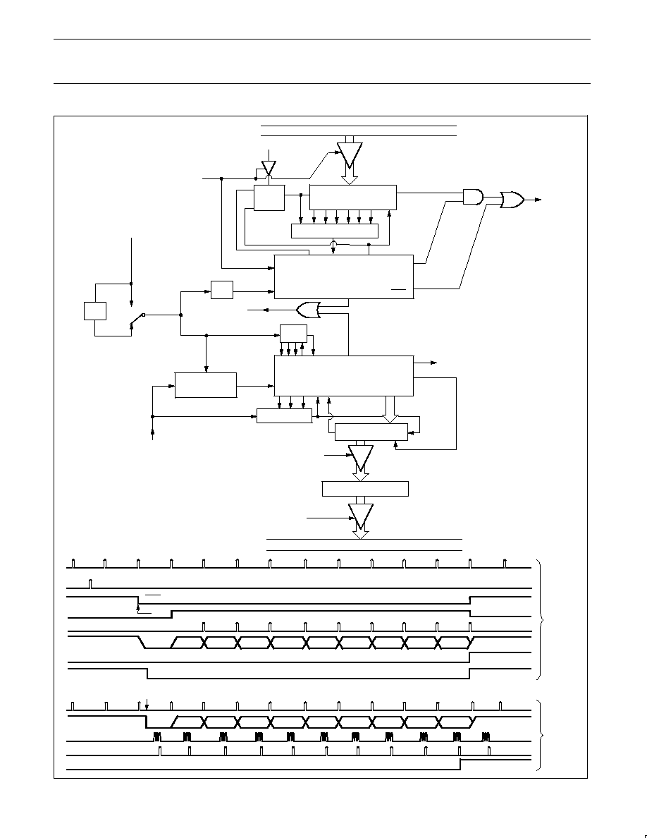
Philips Semiconductors
Product data
P83C654X2/P87C654X2
80C51 8-bit microcontroller family
16 kB OTP/ROM,
256B RAM, low voltage (2.7 to 5.5 V), low power, high speed
(30/33 MHz)
2004 Apr 20
26
80C51 Internal Bus
SBUF
Zero Detector
D Q
S
CL
Write
to
SBUF
TX Control
TX Clock
Send
Data
Start
RX Control
Start
Load
SBUF
RX Clock
T1
Serial
Port
Interrupt
Input Shift Register
(9 Bits)
Load
SBUF
Shift
SBUF
Read
SBUF
80C51 Internal Bus
TxD
TB8
˜
16
1-to-0
Transition
Detector
Sample
˜
2
SMOD = 1
SMOD = 0
Shift
Bit Detector
RxD
Stop Bit
Gen.
Mode 2
Phase 2 Clock
(1/2 f
OSC
)
R1
˜
16
Shift
1FFH
Transmit
Send
S1P1
Shift
TX
Clock
Write to SBUF
Start Bit
TxD
Stop Bit
D0
D1
D2
D3
D4
D5
D6
D7
TI
RX
Clock
˜
16 Reset
Start
Bit
RxD
Stop Bit
D0
D1
D2
D3
D4
D5
D6
D7
Bit Detector
Sample Times
Shift
RI
Receive
Data
(SMOD is
PCON.7)
TB8
RB8
Stop Bit Gen.
SU00541
Figure 17. Serial Port Mode 2
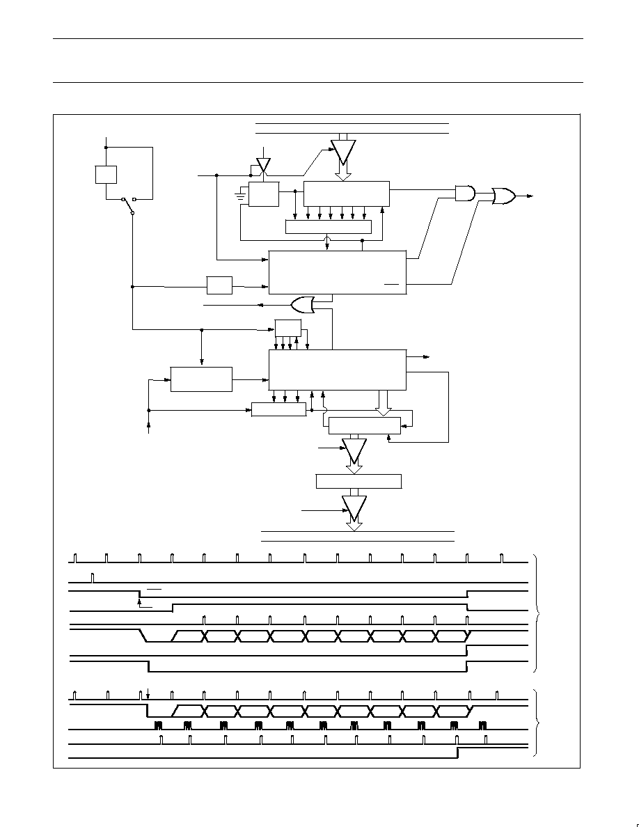
Philips Semiconductors
Product data
P83C654X2/P87C654X2
80C51 8-bit microcontroller family
16 kB OTP/ROM,
256B RAM, low voltage (2.7 to 5.5 V), low power, high speed
(30/33 MHz)
2004 Apr 20
27
80C51 Internal Bus
SBUF
Zero Detector
D Q
S
CL
Write
to
SBUF
TX Control
TX Clock
Send
Data
Start
RX Control
Start
RX Clock
T1
Serial
Port
Interrupt
Input Shift Register
(9 Bits)
Load
SBUF
Shift
SBUF
Read
SBUF
80C51 Internal Bus
TxD
TB8
˜
16
1-to-0
Transition
Detector
Sample
˜
2
Timer 1
Overflow
SMOD = 1
SMOD = 0
Shift
Bit Detector
RxD
R1
˜
16
Load
SBUF
Shift
1FFH
Transmit
Send
S1P1
Shift
TX
Clock
Write to SBUF
Start Bit
TxD
Stop Bit
D0
D1
D2
D3
D4
D5
D6
D7
TI
RX
Clock
˜
16 Reset
Start
Bit
RxD
Stop Bit
D0
D1
D2
D3
D4
D5
D6
D7
Bit Detector
Sample Times
Shift
RI
Receive
Data
TB8
RB8
Stop Bit Gen.
SU00542
Figure 18. Serial Port Mode 3

Philips Semiconductors
Product data
P83C654X2/P87C654X2
80C51 8-bit microcontroller family
16 kB OTP/ROM,
256B RAM, low voltage (2.7 to 5.5 V), low power, high speed
(30/33 MHz)
2004 Apr 20
28
Enhanced Features
The UART operates in all of the usual modes that are described in
the first section of
Data Handbook IC20, 80C51-Based 8-Bit
Microcontrollers. In addition the UART can perform framing error
detect by looking for missing stop bits, and automatic address
recognition. The UART also fully supports multiprocessor
communication as does the standard 80C51 UART.
When used for framing error detect the UART looks for missing stop
bits in the communication. A missing bit will set the FE bit in the
SCON register. The FE bit shares the SCON.7 bit with SM0 and the
function of SCON.7 is determined by PCON.6 (SMOD0) (see
Figure 13). If SMOD0 is set then SCON.7 functions as FE. SCON.7
functions as SM0 when SMOD0 is cleared. When used as FE
SCON.7 can only be cleared by software. Refer to Figure 19.
Automatic Address Recognition
Automatic Address Recognition is a feature which allows the UART
to recognize certain addresses in the serial bit stream by using
hardware to make the comparisons. This feature saves a great deal
of software overhead by eliminating the need for the software to
examine every serial address which passes by the serial port. This
feature is enabled by setting the SM2 bit in SCON. In the 9 bit UART
modes, mode 2 and mode 3, the Receive Interrupt flag (RI) will be
automatically set when the received byte contains either the "Given"
address or the "Broadcast" address. The 9-bit mode requires that
the 9th information bit is a 1 to indicate that the received information
is an address and not data. Automatic address recognition is shown
in Figure 20.
The 8 bit mode is called Mode 1. In this mode the RI flag will be set
if SM2 is enabled and the information received has a valid stop bit
following the 8 address bits and the information is either a Given or
Broadcast address.
Mode 0 is the Shift Register mode and SM2 is ignored.
Using the Automatic Address Recognition feature allows a master to
selectively communicate with one or more slaves by invoking the
Given slave address or addresses. All of the slaves may be
contacted by using the Broadcast address. Two special Function
Registers are used to define the slave's address, SADDR, and the
address mask, SADEN. SADEN is used to define which bits in the
SADDR are to b used and which bits are "don't care". The SADEN
mask can be logically ANDed with the SADDR to create the "Given"
address which the master will use for addressing each of the slaves.
Use of the Given address allows multiple slaves to be recognized
while excluding others. The following examples will help to show the
versatility of this scheme:
Slave 0
SADDR
=
1100 0000
SADEN
=
1111 1101
Given
=
1100 00X0
Slave 1
SADDR
=
1100 0000
SADEN
=
1111 1110
Given
=
1100 000X
In the above example SADDR is the same and the SADEN data is
used to differentiate between the two slaves. Slave 0 requires a 0 in
bit 0 and it ignores bit 1. Slave 1 requires a 0 in bit 1 and bit 0 is
ignored. A unique address for Slave 0 would be 1100 0010 since
slave 1 requires a 0 in bit 1. A unique address for slave 1 would be
1100 0001 since a 1 in bit 0 will exclude slave 0. Both slaves can be
selected at the same time by an address which has bit 0 = 0 (for
slave 0) and bit 1 = 0 (for slave 1). Thus, both could be addressed
with 1100 0000.
In a more complex system the following could be used to select
slaves 1 and 2 while excluding slave 0:
Slave 0
SADDR
=
1100 0000
SADEN
=
1111 1001
Given
=
1100 0XX0
Slave 1
SADDR
=
1110 0000
SADEN
=
1111 1010
Given
=
1110 0X0X
Slave 2
SADDR
=
1110 0000
SADEN
=
1111 1100
Given
=
1110 00XX
In the above example the differentiation among the 3 slaves is in the
lower 3 address bits. Slave 0 requires that bit 0 = 0 and it can be
uniquely addressed by 1110 0110. Slave 1 requires that bit 1 = 0 and
it can be uniquely addressed by 1110 and 0101. Slave 2 requires
that bit 2 = 0 and its unique address is 1110 0011. To select Slaves 0
and 1 and exclude Slave 2 use address 1110 0100, since it is
necessary to make bit 2 = 1 to exclude slave 2.
The Broadcast Address for each slave is created by taking the
logical OR of SADDR and SADEN. Zeros in this result are trended
as don't-cares. In most cases, interpreting the don't-cares as ones,
the broadcast address will be FF hexadecimal.
Upon reset SADDR (SFR address 0A9H) and SADEN (SFR
address 0B9H) are leaded with 0s. This produces a given address
of all "don't cares" as well as a Broadcast address of all "don't
cares". This effectively disables the Automatic Addressing mode and
allows the microcontroller to use standard 80C51 type UART drivers
which do not make use of this feature.
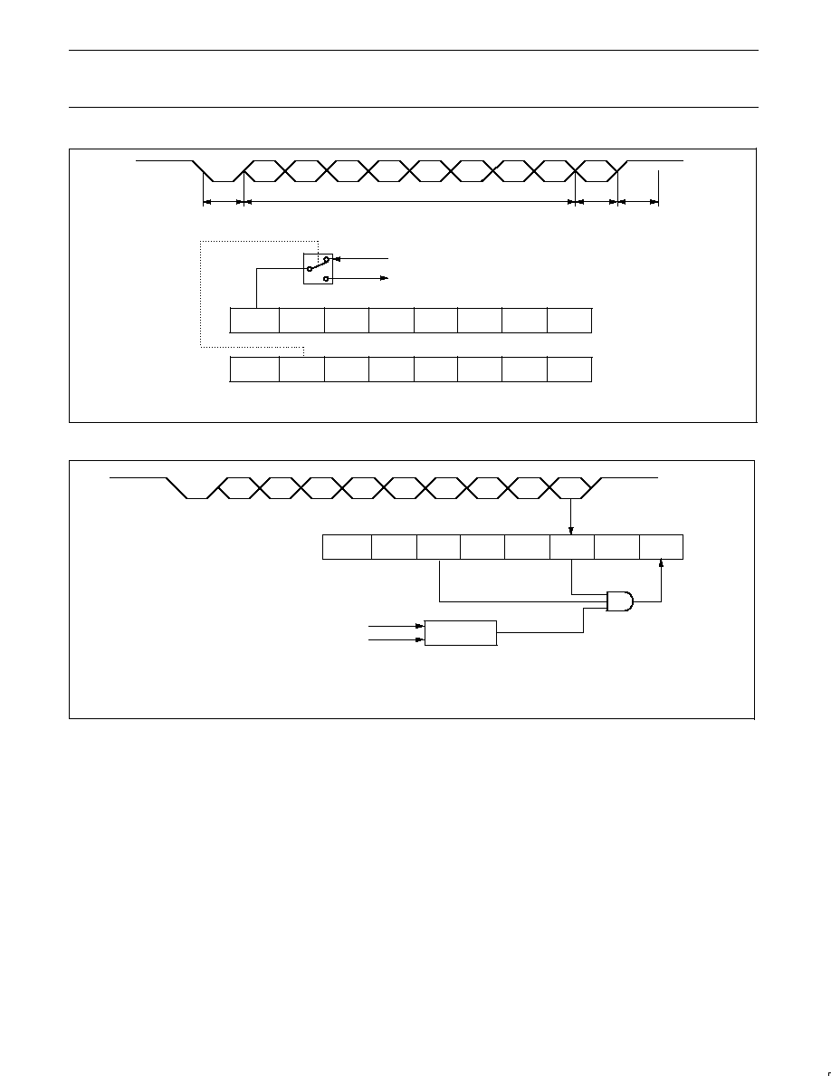
Philips Semiconductors
Product data
P83C654X2/P87C654X2
80C51 8-bit microcontroller family
16 kB OTP/ROM,
256B RAM, low voltage (2.7 to 5.5 V), low power, high speed
(30/33 MHz)
2004 Apr 20
29
SMOD1
SMOD0
≠
POF
LVF
GF0
GF1
IDL
PCON
(87H)
SM0 / FE
SM1
SM2
REN
TB8
RB8
TI
RI
SCON
(98H)
D0
D1
D2
D3
D4
D5
D6
D7
D8
STOP
BIT
DATA BYTE
ONLY IN
MODE 2, 3
START
BIT
SET FE BIT IF STOP BIT IS 0 (FRAMING ERROR)
SM0 TO UART MODE CONTROL
0 : SCON.7 = SM0
1 : SCON.7 = FE
SU00044
Figure 19. UART Framing Error Detection
SM0
SM1
SM2
REN
TB8
RB8
TI
RI
SCON
(98H)
D0
D1
D2
D3
D4
D5
D6
D7
D8
1
1
1
0
COMPARATOR
1
1
X
RECEIVED ADDRESS D0 TO D7
PROGRAMMED ADDRESS
IN UART MODE 2 OR MODE 3 AND SM2 = 1:
INTERRUPT IF REN=1, RB8=1 AND "RECEIVED ADDRESS" = "PROGRAMMED ADDRESS"
≠ WHEN OWN ADDRESS RECEIVED, CLEAR SM2 TO RECEIVE DATA BYTES
≠ WHEN ALL DATA BYTES HAVE BEEN RECEIVED: SET SM2 TO WAIT FOR NEXT ADDRESS.
SU00045
Figure 20. UART Multiprocessor Communication, Automatic Address Recognition

Philips Semiconductors
Product data
P83C654X2/P87C654X2
80C51 8-bit microcontroller family
16 kB OTP/ROM,
256B RAM, low voltage (2.7 to 5.5 V), low power, high speed
(30/33 MHz)
2004 Apr 20
30
I
2
C-bus Serial I/O
The I
2
C-bus serial port is identical to the I
2
C-bus serial port on the
8xC554 and 8xC652 devices.
Note that in the P8xC654X2, the I
2
C-bus pins are alternate functions
to port pins P1.6 and P1.7. Because of this, P1.6 and P1.7 on these
parts do not have a pull-up structure as found on the 80C51; P1.6
and P1.7 have open drain outputs.
The I
2
C-bus uses two wires (SDA and SCL) to transfer information
between devices connected to the bus. The main features of the bus
are:
≠ Bidirectional data transfer between masters and slaves
≠ Multimaster bus (no central master)
≠ Arbitration between simultaneously transmitting masters without
corruption of serial data on the bus
≠ Serial clock synchronization allows devices with different bit rates
to communicate via one serial bus
≠ Serial clock synchronization can be used as a handshake
mechanism to suspend and resume serial transfer
≠ The I
2
C-bus may be used for test and diagnostic purposes
The output latches of P1.6 and P1.7 must be set to logic 1 in order
to enable I
2
C-bus.
The P8xC654X2 on-chip I
2
C-bus logic provides a serial interface
that meets the I
2
C-bus specification and supports all transfer modes
(other than the low-speed mode) from and to the I
2
C-bus. The
I
2
C-bus logic handles bytes transfer autonomously. It also keeps
track of serial transfers, and a status register (S1STA) reflects the
status of the I
2
C-bus.
The CPU interfaces to the I
2
C-bus logic via the following four special
function registers: S1CON (I
2
C-bus control register), S1STA
(I
2
C-bus status register), S1DAT (I
2
C-bus data register), and
S1ADR (I
2
C-bus slave address register). The I
2
C-bus logic
interfaces to the external I
2
C-bus via two port 1 pins: P1.6/SCL
(serial clock line) and P1.7/SDA (serial data line).
A typical I
2
C-bus configuration is shown in Figure 21, and Figure 22
shows how a data transfer is accomplished on the bus. Depending
on the state of the direction bit (R/W), two types of data transfers are
possible on the I
2
C-bus:
1. Data transfer from a master transmitter to a slave receiver. The
first byte transmitted by the master is the slave address. Next
follows a number of data bytes. The slave returns an
acknowledge bit after each received byte.
2. Data transfer from a slave transmitter to a master receiver. The
first byte (the slave address) is transmitted by the master. The
slave then returns an acknowledge bit. Next follows the data
bytes transmitted by the slave to the master. The master returns
an acknowledge bit after all received bytes other than the last
byte. At the end of the last received byte, a "not acknowledge" is
returned.
The master device generates all of the serial clock pulses and the
START and STOP conditions. A transfer is ended with a STOP
condition or with a repeated START condition. Since a repeated
START condition is also the beginning of the next serial transfer, the
I
2
C-bus will not be released.
Modes of Operation: The on-chip I
2
C-bus logic may operate in the
following four modes:
1. Master Transmitter Mode:
Serial data output through P1.7/SDA while P1.6/SCL outputs the
serial clock. The first byte transmitted contains the slave address
of the receiving device (7 bits) and the data direction bit. In this
case the data direction bit (R/W) will be logic 0, and we say that
a "W" is transmitted. Thus the first byte transmitted is SLA+W.
Serial data is transmitted 8 bits at a time. After each byte is
transmitted, an acknowledge bit is received. START and STOP
conditions are output to indicate the beginning and the end of a
serial transfer.
2. Master Receiver Mode:
The first byte transmitted contains the slave address of the
transmitting device (7 bits) and the data direction bit. In this case
the data direction bit (R/W) will be logic 1, and we say that an "R"
is transmitted. Thus the first byte transmitted is SLA+R. Serial
data is received via P1.7/SDA while P1.6/SCL outputs the serial
clock. Serial data is received 8 bits at a time. After each byte is
received, an acknowledge bit is transmitted. START and STOP
conditions are output to indicate the beginning and end of a
serial transfer.
3. Slave Receiver Mode:
Serial data and the serial clock are received through P1.7/SDA
and P1.6/SCL. After each byte is received, an acknowledge bit is
transmitted. START and STOP conditions are recognized as the
beginning and end of a serial transfer. Address recognition is
performed by hardware after reception of the slave address and
direction bit.
4. Slave Transmitter Mode:
The first byte is received and handled as in the slave receiver
mode. However, in this mode, the direction bit will indicate that
the transfer direction is reversed. Serial data is transmitted via
P1.7/SDA while the serial clock is input through P1.6/SCL.
START and STOP conditions are recognized as the beginning
and end of a serial transfer.
In a given application, I
2
C-bus may operate as a master and as a
slave. In the slave mode, the I
2
C-bus hardware looks for its own
slave address and the general call address. If one of these
addresses is detected, an interrupt is requested. When the
microcontroller wishes to become the bus master, the hardware
waits until the bus is free before the master mode is entered so that
a possible slave action is not interrupted. If bus arbitration is lost in
the master mode, the I
2
C-bus switches to the slave mode
immediately and can detect its own slave address in the same serial
transfer.

Philips Semiconductors
Product data
P83C654X2/P87C654X2
80C51 8-bit microcontroller family
16 kB OTP/ROM,
256B RAM, low voltage (2.7 to 5.5 V), low power, high speed
(30/33 MHz)
2004 Apr 20
31
VDD
OTHER DEVICE WITH
I2C-BUS INTERFACE
P8xC654X2
OTHER DEVICE WITH
I2C-BUS INTERFACE
P1.7/SDA
P1.6/SCL
SDA
SCL
I2C-bus
RP
RP
SU01734
Figure 21. Typical I
2
C-bus configuration
SCL
START
CONDITION
S
SDA
P/S
MSB
ACKNOWLEDGMENT
SIGNAL FROM RECEIVER
CLOCK LINE HELD LOW WHILE
INTERRUPTS ARE SERVICED
1
2
7
8
9
1
2
3≠8
ACK
9
ACK
REPEATED IF MORE BYTES
ARE TRANSFERRED
ACKNOWLEDGMENT
SIGNAL FROM RECEIVER
SLAVE ADDRESS
R/W
DIRECTION
BIT
STOP
CONDITION
REPEATED
START
CONDITION
SU00965
Figure 22. Data Transfer on the I
2
C-bus
I
2
C-bus Implementation and Operation: Figure 23 shows how the
on-chip I
2
C-bus interface is implemented, and the following text
describes the individual blocks.
I
NPUT
F
ILTERS
AND
O
UTPUT
S
TAGES
The input filters have I
2
C-bus compatible input levels. If the input
voltage is less than 1.5 V, the input logic level is interpreted as 0; if
the input voltage is greater than 3.0 V, the input logic level is
interpreted as 1. Input signals are synchronized with the internal
clock (f
OSC
/4), and spikes shorter than three oscillator periods are
filtered out.
The output stages consist of open drain transistors that can sink
3mA at V
OUT
< 0.4 V. These open drain outputs do not have
clamping diodes to V
DD
. Thus, if the device is connected to the
I
2
C-bus and V
DD
is switched off, the I
2
C-bus is not affected.
A
DDRESS
R
EGISTER,
S
1
ADR
This 8-bit special function register may be loaded with the 7-bit slave
address (7 most significant bits) to which the I
2
C-bus will respond
when programmed as a slave transmitter or receiver. The LSB (GC)
is used to enable general call address (00H) recognition.
C
OMPARATOR
The comparator compares the received 7-bit slave address with its
own slave address (7 most significant bits in S1ADR). It also
compares the first received 8-bit byte with the general call address
(00H). If an equality is found, the appropriate status bits are set and
an interrupt is requested.
S
HIFT
R
EGISTER,
S
1
DAT
This 8-bit special function register contains a byte of serial data to
be transmitted or a byte which has just been received. Data in
S1DAT is always shifted from right to left; the first bit to be
transmitted is the MSB (bit 7) and, after a byte has been received,
the first bit of received data is located at the MSB of S1DAT. While
data is being shifted out, data on the bus is simultaneously being
shifted in; S1DAT always contains the last byte present on the bus.
Thus, in the event of lost arbitration, the transition from master
transmitter to slave receiver is made with the correct data in S1DAT.
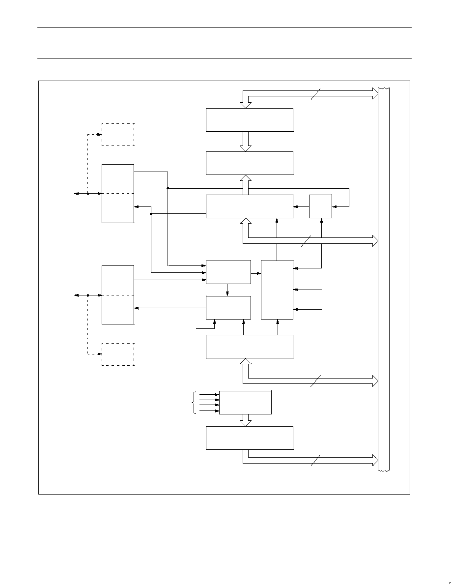
Philips Semiconductors
Product data
P83C654X2/P87C654X2
80C51 8-bit microcontroller family
16 kB OTP/ROM,
256B RAM, low voltage (2.7 to 5.5 V), low power, high speed
(30/33 MHz)
2004 Apr 20
32
fOSC/4
INTERNAL
BUS
ADDRESS REGISTER
COMPARATOR
SHIFT REGISTER
CONTROL REGISTER
STATUS REGISTER
ARBITRATION &
SYNC LOGIC
TIMING
&
CONTROL
LOGIC
SERIAL CLOCK
GENERATOR
ACK
STATUS
DECODER
TIMER 1
OVERFLOW
INTERRUPT
8
8
8
8
S1STA
STATUS BITS
S1CON
S1DAT
INPUT
FILTER
OUTPUT
STAGE
P1.7
INPUT
FILTER
OUTPUT
STAGE
P1.6
P1.6/SCL
P1.7/SDA
S1ADR
su00966
Figure 23. I
2
C-bus Serial Interface Block Diagram

Philips Semiconductors
Product data
P83C654X2/P87C654X2
80C51 8-bit microcontroller family
16 kB OTP/ROM,
256B RAM, low voltage (2.7 to 5.5 V), low power, high speed
(30/33 MHz)
2004 Apr 20
33
A
RBITRATION
AND
S
YNCHRONIZATION
L
OGIC
In the master transmitter mode, the arbitration logic checks that
every transmitted logic 1 actually appears as a logic 1 on the
I
2
C-bus. If another device on the bus overrules a logic 1 and pulls
the SDA line LOW, arbitration is lost, and the I
2
C-bus immediately
changes from master transmitter to slave receiver. The I
2
C-bus will
continue to output clock pulses (on SCL) until transmission of the
current serial byte is complete.
Arbitration may also be lost in the master receiver mode. Loss of
arbitration in this mode can only occur while the I
2
C-bus is returning
a "not acknowledge: (logic 1) to the bus. Arbitration is lost when
another device on the bus pulls this signal LOW. Since this can
occur only at the end of a serial byte, the I
2
C-bus generates no
further clock pulses. Figure 24 shows the arbitration procedure.
The synchronization logic will synchronize the serial clock generator
with the clock pulses on the SCL line from another device. If two or
more master devices generate clock pulses, the "mark" duration is
determined by the device that generates the shortest "marks," and
the "space" duration is determined by the device that generates the
longest "spaces." Figure 25 shows the synchronization procedure.
A slave may stretch the space duration to slow down the bus
master. The space duration may also be stretched for handshaking
purposes. This can be done after each bit or after a complete byte
transfer. The I
2
C-bus will stretch the SCL space duration after a byte
has been transmitted or received and the acknowledge bit has been
transferred. The serial interrupt flag (SI) is set, and the stretching
continues until the serial interrupt flag is cleared.
ACK
1. Another device transmits identical serial data.
SDA
1
2
3
4
8
9
SCL
(1)
(1)
(2)
(3)
2. Another device overrules a logic 1 (dotted line) transmitted by SIO1 (master) by pulling the SDA line low. Arbitration is
lost, and SIO1 enters the slave receiver mode.
3. SIO1 is in the slave receiver mode but still generates clock pulses until the current byte has been transmitted. SIO1 will
not generate clock pulses for the next byte. Data on SDA originates from the new master once it has won arbitration.
SU00967
Figure 24. Arbitration Procedure
(1)
SCL
(3)
(1)
SDA
MARK
DURATION
SPACE DURATION
(2)
1. Another service pulls the SCL line low before the SIO1 "mark" duration is complete. The serial clock generator is immediately
reset and commences with the "space" duration by pulling SCL low.
2. Another device still pulls the SCL line low after SIO1 releases SCL. The serial clock generator is forced into the wait state
until the SCL line is released.
3. The SCL line is released, and the serial clock generator commences with the mark duration.
SU00968
Figure 25. Serial Clock Synchronization

Philips Semiconductors
Product data
P83C654X2/P87C654X2
80C51 8-bit microcontroller family
16 kB OTP/ROM,
256B RAM, low voltage (2.7 to 5.5 V), low power, high speed
(30/33 MHz)
2004 Apr 20
34
S
ERIAL
C
LOCK
G
ENERATOR
This programmable clock pulse generator provides the SCL clock
pulses when the I
2
C-bus is in the master transmitter or master
receiver mode. It is switched off when the I
2
C-bus is in a slave
mode. In standard speed mode, the programmable output clock
frequencies are: f
OSC
/120, f
OSC
/9600, and the Timer 1 overflow rate
divided by eight. The output clock pulses have a 50 % duty cycle
unless the clock generator is synchronized with other SCL clock
sources as described above.
T
IMING
AND
C
ONTROL
The timing and control logic generates the timing and control signals
for serial byte handling. This logic block provides the shift pulses for
S1DAT, enables the comparator, generates and detects start and
stop conditions, receives and transmits acknowledge bits, controls
the master and slave modes, contains interrupt request logic, and
monitors the I
2
C-bus status.
C
ONTROL
R
EGISTER,
S
1
CON
This 7-bit special function register is used by the microcontroller to
control the following I
2
C-bus functions: start and restart of a serial
transfer, termination of a serial transfer, bit rate, address recognition,
and acknowledgment.
S
TATUS
D
ECODER
AND
S
TATUS
R
EGISTER
The status decoder takes all of the internal status bits and
compresses them into a 5-bit code. This code is unique for each
I
2
C-bus status. The 5-bit code may be used to generate vector
addresses for fast processing of the various service routines. Each
service routine processes a particular bus status. There are 26
possible bus states if all four modes of the I
2
C-bus are used. The
5-bit status code is latched into the five most significant bits of the
status register when the serial interrupt flag is set (by hardware) and
remains stable until the interrupt flag is cleared by software. The
three least significant bits of the status register are always zero. If
the status code is used as a vector to service routines, then the
routines are displaced by eight address locations. Eight bytes of
code is sufficient for most of the service routines (see the software
example in this section).
The Four I
2
C-bus Special Function Registers: The
microcontroller interfaces to the I
2
C-bus via four special function
registers. These four SFRs (S1ADR, S1DAT, S1CON, and S1STA)
are described individually in the following sections.
The Address Register, S1ADR: The CPU can read from and write
to this 8-bit, directly addressable SFR. S1ADR is not affected by the
the I
2
C-bus hardware. The contents of this register are irrelevant
when the I
2
C-bus is in a master mode. In the slave modes, the
seven most significant bits must be loaded with the microcontroller's
own slave address, and, if the least significant bit is set, the general
call address (00H) is recognized; otherwise it is ignored.
S1ADR
(DBH)
X
GC
7
6
5
4
3
2
1
0
own slave address
X
X
X
X
X
X
The most significant bit corresponds to the first bit received from the
I
2
C-bus after a start condition. A logic 1 in S1ADR corresponds to a
HIGH level on the I
2
C-bus, and a logic 0 corresponds to a LOW
level on the bus.
The Data Register, S1DAT: S1DAT contains a byte of serial data to
be transmitted or a byte which has just been received. The CPU can
read from and write to this 8-bit, directly addressable SFR while it is
not in the process of shifting a byte. This occurs when the I
2
C-bus is
in a defined state and the serial interrupt flag is set. Data in S1DAT
remains stable as long as SI is set. Data in S1DAT is always shifted
from right to left: the first bit to be transmitted is the MSB (bit 7), and,
after a byte has been received, the first bit of received data is
located at the MSB of S1DAT. While data is being shifted out, data
on the bus is simultaneously being shifted in; S1DAT always
contains the last data byte present on the bus. Thus, in the event of
lost arbitration, the transition from master transmitter to slave
receiver is made with the correct data in S1DAT.
S1DAT
(DAH)
SD7
SD6
SD5
SD4
SD3
SD2
SD1
SD0
7
6
5
4
3
2
1
0
shift direction
SD7 - SD0:
Eight bits to be transmitted or just received. A logic 1 in S1DAT
corresponds to a HIGH level on the I
2
C-bus, and a logic 0
corresponds to a LOW level on the bus. Serial data shifts through
S1DAT from right to left. Figure 26 shows how data in S1DAT is
serially transferred to and from the SDA line.
S1DAT and the ACK flag form a 9-bit shift register which shifts in or
shifts out an 8-bit byte, followed by an acknowledge bit. The ACK
flag is controlled by the I
2
C-bus hardware and cannot be accessed
by the CPU. Serial data is shifted through the ACK flag into S1DAT
on the rising edges of serial clock pulses on the SCL line. When a
byte has been shifted into S1DAT, the serial data is available in
S1DAT, and the acknowledge bit is returned by the control logic
during the ninth clock pulse. Serial data is shifted out from S1DAT
via a buffer (BSD7) on the falling edges of clock pulses on the SCL
line.
When the CPU writes to S1DAT, BSD7 is loaded with the content of
S1DAT.7, which is the first bit to be transmitted to the SDA line (see
Figure 27). After nine serial clock pulses, the eight bits in S1DAT will
have been transmitted to the SDA line, and the acknowledge bit will
be present in ACK. Note that the eight transmitted bits are shifted
back into S1DAT.
The Control Register, S1CON: The CPU can read from and write
to this 8-bit, directly addressable SFR. Two bits are affected by the
I
2
C hardware: the SI bit is set when a serial interrupt is requested,
and the STO bit is cleared when a STOP condition is present on the
I
2
C-bus. The STO bit is also cleared when ENS1 = 0.
S1CON
(D8H)
ENS1
STA
STO
SI
AA
CR1
CR0
7
6
5
4
3
2
1
0
CR2
ENS
1,
THE
I
2
C E
NABLE
B
IT
ENS1 = 0: When ENS1 is logic 0, the SDA and SCL outputs are in a
high impedance state. SDA and SCL input signals are ignored, I
2
C
is in the "not addressed" slave state, and the STO bit in S1CON is
forced to 0. No other bits are affected. P1.6 and P1.7 may be used
as open drain I/O ports.
ENS1 = 1: When ENS1 is "1", I
2
C is enabled. The P1.6 and P1.7
port latches must be set to logic 1.
ENS1 should not be used to temporarily release I
2
C from the
I
2
C-bus since, when ENS1 is reset, the I
2
C-bus status is lost. The
AA flag should be used instead (see description of the AA flag in the
following text).
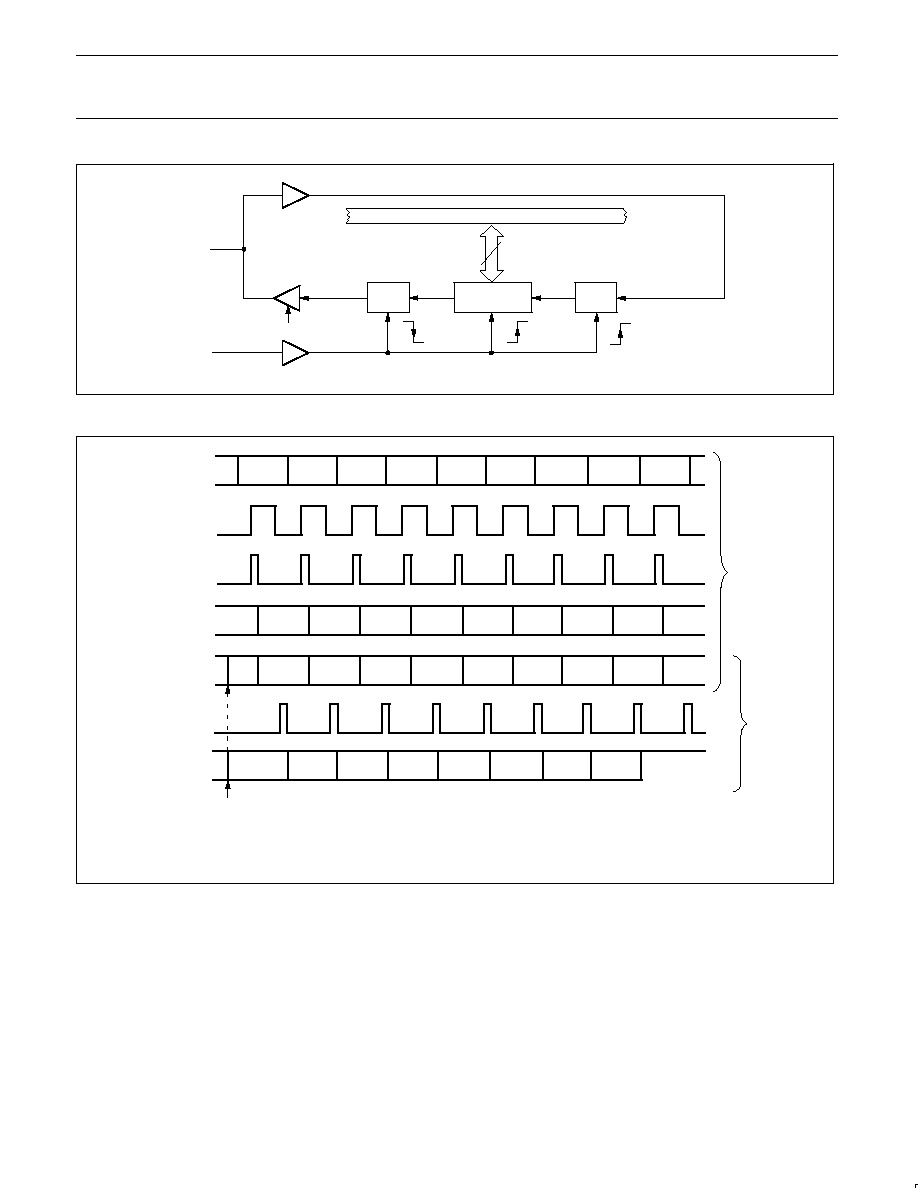
Philips Semiconductors
Product data
P83C654X2/P87C654X2
80C51 8-bit microcontroller family
16 kB OTP/ROM,
256B RAM, low voltage (2.7 to 5.5 V), low power, high speed
(30/33 MHz)
2004 Apr 20
35
INTERNAL BUS
8
BSD7
S1DAT
ACK
SCL
SDA
SHIFT PULSES
SU00969
Figure 26. Serial Input/Output Configuration
SHIFT IN
SDA
SCL
D7
D6
D5
D4
D3
D2
D1
D0
A
SHIFT ACK & S1DAT
ACK
(2)
(2)
(2)
(2)
(2)
(2)
(2)
(2)
A
(2)
(2)
(2)
(2)
(2)
(2)
(2)
(2)
(1)
(1)
S1DAT
SHIFT BSD7
BSD7
D7
D6
D5
D4
D3
D2
D1
D0
(3)
LOADED BY THE CPU
(1) Valid data in S1DAT
(2) Shifting data in S1DAT and ACK
(3) High level on SDA
SHIFT OUT
SU00970
Figure 27. Shift-in and Shift-out Timing
In the following text, it is assumed that ENS1 = 1.
STA
,
THE
START F
LAG
STA = 1: When the STA bit is set to enter a master mode, the I
2
C
hardware checks the status of the I
2
C-bus and generates a START
condition if the bus is free. If the bus is not free, then I
2
C waits for a
STOP condition (which will free the bus) and generates a START
condition after a delay of a half clock period of the internal serial
clock generator.
If STA is set while I
2
C is already in a master mode and one or more
bytes are transmitted or received, I
2
C transmits a repeated START
condition. STA may be set at any time. STA may also be set when
I
2
C is an addressed slave.
STA = 0: When the STA bit is reset, no START condition or repeated
START condition will be generated.
STO
,
THE
STOP F
LAG
STO = 1: When the STO bit is set while I
2
C is in a master mode, a
STOP condition is transmitted to the I
2
C-bus. When the STOP
condition is detected on the bus, the I
2
C hardware clears the STO
flag. In a slave mode, the STO flag may be set to recover from an
error condition. In this case, no STOP condition is transmitted to the
I
2
C-bus. However, the I
2
C hardware behaves as if a STOP condition
has been received and switches to the defined "not addressed"
slave receiver mode. The STO flag is automatically cleared by
hardware.

Philips Semiconductors
Product data
P83C654X2/P87C654X2
80C51 8-bit microcontroller family
16 kB OTP/ROM,
256B RAM, low voltage (2.7 to 5.5 V), low power, high speed
(30/33 MHz)
2004 Apr 20
36
If the STA and STO bits are both set, the a STOP condition is
transmitted to the I
2
C-bus if I
2
C is in a master mode (in a slave
mode, I
2
C generates an internal STOP condition which is not
transmitted). I
2
C then transmits a START condition.
STO = 0: When the STO bit is reset, no STOP condition will be
generated.
SI
,
THE
S
ERIAL
I
NTERRUPT
F
LAG
SI = 1: When the SI flag is set, then, if the EA and ES1 (interrupt
enable register) bits are also set, a serial interrupt is requested. SI is
set by hardware when one of 25 of the 26 possible I
2
C states is
entered. The only state that does not cause SI to be set is state
F8H, which indicates that no relevant state information is available.
While SI is set, the LOW period of the serial clock on the SCL line is
stretched, and the serial transfer is suspended. A HIGH level on the
SCL line is unaffected by the serial interrupt flag. SI must be reset
by software.
SI = 0: When the SI flag is reset, no serial interrupt is requested, and
there is no stretching of the serial clock on the SCL line.
AA
,
THE
A
SSERT
A
CKNOWLEDGE
F
LAG
AA = 1: If the AA flag is set, an acknowledge (low level to SDA) will
be returned during the acknowledge clock pulse on the SCL line
when:
≠ The "own slave address" has been received
≠ The general call address has been received while the general call
bit (GC) in S1ADR is set
≠ A data byte has been received while I
2
C is in the master receiver
mode
≠ A data byte has been received while I
2
C is in the addressed slave
receiver mode
AA = 0: if the AA flag is reset, a not acknowledge (HIGH level to
SDA) will be returned during the acknowledge clock pulse on SCL
when:
≠ A data has been received while I
2
C is in the master receiver mode
≠ A data byte has been received while I
2
C is in the addressed slave
receiver mode
When I
2
C is in the addressed slave transmitter mode, state C8H will
be entered after the last serial is transmitted (see Figure 31). When
SI is cleared, I
2
C leaves state C8H, enters the not addressed slave
receiver mode, and the SDA line remains at a HIGH level. In state
C8H, the AA flag can be set again for future address recognition.
When I
2
C is in the not addressed slave mode, its own slave address
and the general call address are ignored. Consequently, no
acknowledge is returned, and a serial interrupt is not requested.
Thus, I
2
C can be temporarily released from the I
2
C-bus while the
bus status is monitored. While I
2
C is released from the bus, START
and STOP conditions are detected, and serial data is shifted in.
Address recognition can be resumed at any time by setting the AA
flag. If the AA flag is set when the part's own slave address or the
general call address has been partly received, the address will be
recognized at the end of the byte transmission.
CR
0,
CR
1,
AND
CR
2,
THE
C
LOCK
R
ATE
B
ITS
These three bits determine the serial clock frequency when I
2
C is in
a master mode. The various serial rates are shown in Table 7.
If the I
2
C block is to be used in fast mode, bit 3 in AUXR must be
set. The user can read but cannot write (write once) to AUXR after
setup.
AUXR
(8EH)
≠
A0
7
6
5
4
3
2
1
0
≠
≠
≠
FAST/
STD
I
2
C
≠
≠
A 12.5kHz bit rate may be used by devices that interface to the
I
2
C-bus via standard I/O port lines which are software driven and
slow. 100kHz is usually the maximum bit rate and can be derived
from a 16 MHz, 12 MHz, or a 6 MHz oscillator. A variable bit rate
(0.5kHz to 62.5kHz) may also be used if Timer 1 is not required for
any other purpose while I
2
C is in a master mode.
The frequencies shown in Table 7 are unimportant when I
2
C is in a
slave mode. In the slave modes, I
2
C will automatically synchronize
with any clock frequency up to 100kHz.
The Status Register, S1STA: S1STA is an 8-bit read-only special
function register. The three least significant bits are always zero.
The five most significant bits contain the status code. There are 26
possible status codes. When S1STA contains F8H, no relevant state
information is available and no serial interrupt is requested. All other
S1STA values correspond to defined I
2
C states. When each of
these states is entered, a serial interrupt is requested (SI = 1). A
valid status code is present in S1STA one machine cycle after SI is
set by hardware and is still present one machine cycle after SI has
been reset by software.
Philips Semiconductors
Product data
P83C654X2/P87C654X2
80C51 8-bit microcontroller family
16 kB OTP/ROM,
256B RAM, low voltage (2.7 to 5.5 V), low power, high speed
(30/33 MHz)
2004 Apr 20
37
Table 7.
Serial Clock Rates
6 clock mode
BIT FREQUENCY (kHz) AT f
osc
f
osc
DIVIDED BY
CR2
CR1
CR0
3MHz
6MHz
8MHz
12MHz
15MHz
0
0
0
23
47
62.5
94
117
128
0
0
1
27
54
71
107
134
112
0
1
0
31
63
83.3
125
156
96
0
1
1
37
75
100
150
188
80
1
0
0
6.25
12.5
17
25
31
480
1
0
1
50
100
133
200
250
60
1
1
0
100
200
267
400
500
30
1
1
1
0.24<62.5
0 < 255
0.49 < 62.5
0 < 254
0.65 < 55.6
0 < 253
0.98 < 50.0
0 < 251
1.22 < 52.1
0 < 250
48
◊
(256≠ (reload value Timer1))
Reload value Timer 1 in Mode 2.
12 clock mode
BIT FREQUENCY (kHz) AT f
osc
f
osc
DIVIDED BY
CR2
CR1
CR0
6MHz
12MHz
16MHz
24MHz
30MHz
0
0
0
23
47
62.5
94
117
256
0
0
1
27
54
71
107
134
224
0
1
0
31
63
83.3
125
156
192
0
1
1
37
75
100
150
188
160
1
0
0
6.25
12.5
17
25
31
960
1
0
1
50
100
133
200
250
120
1
1
0
100
200
267
400
500
60
1
1
1
0.24<62.5
0 < 255
0.49 < 62.5
0 < 254
0.65 < 55.6
0 < 253
0.98 < 50.0
0 < 251
1.22 < 52.1
0 < 250
96
◊
(256 ≠(reload value Timer1))
Reload value Timer 1 in Mode 2.
NOTES:
1. These frequencies exceed the upper limit of 100kHz of the I
2
C-bus specification and cannot be used in an I
2
C-bus application.
2. At f
osc
= 24 MHz/30 MHz the maximum I
2
C-bus rate of 100kHz cannot be realized due to the fixed divider rates.
Table 8.
Selection of I
2
C-bus bit rate (Fast mode)
BIT FREQUENCY (kHz) AT f
osc
CR2
CR1
CR0
12 MHz
16 MHz
1
0
0
50
66.7
1
0
1
3.75
5
1
1
0
75
100
1
1
1
100
0
0
0
0
200
1
266.7
1
0
0
1
7.5
10
0
1
0
300
1
400
1
0
1
1
400
1
≠
NOTES:
1. These bit rates are for "fast-mode" I
2
C-bus applications and cannot be used for bit rates up to 100 kbit/sec.
2. Serial status register S1STA is a read only register.
Philips Semiconductors
Product data
P83C654X2/P87C654X2
80C51 8-bit microcontroller family
16 kB OTP/ROM,
256B RAM, low voltage (2.7 to 5.5 V), low power, high speed
(30/33 MHz)
2004 Apr 20
38
More Information on I
2
C Operating Modes: The four operating
modes are:
≠ Master Transmitter
≠ Master Receiver
≠ Slave Receiver
≠ Slave Transmitter
Data transfers in each mode of operation are shown in Figures
28≠31. These figures contain the following abbreviations:
Abbreviation
Explanation
S
Start condition
SLA
7-bit slave address
R
Read bit (HIGH level at SDA)
W
Write bit (low level at SDA)
A
Acknowledge bit (low level at SDA)
A
Not acknowledge bit (HIGH level at SDA)
Data
8-bit data byte
P
Stop condition
In Figures 28-31, circles are used to indicate when the serial
interrupt flag is set. The numbers in the circles show the status code
held in the S1STA register. At these points, a service routine must
be executed to continue or complete the serial transfer. These
service routines are not critical since the serial transfer is suspended
until the serial interrupt flag is cleared by software.
When a serial interrupt routine is entered, the status code in S1STA
is used to branch to the appropriate service routine. For each status
code, the required software action and details of the following serial
transfer are given in Tables 9-13.
Master Transmitter Mode: In the master transmitter mode, a
number of data bytes are transmitted to a slave receiver (see
Figure 28). Before the master transmitter mode can be entered,
S1CON must be initialized as follows:
S1CON
(D8H)
CR2
ENS1
STA
STO
SI
AA
CR1
CR0
7
6
5
4
3
2
1
0
1
0
0
0
X
bit rate
bit
rate
CR0, CR1, and CR2 define the serial bit rate. ENS1 must be set to
logic 1 to enable I
2
C. If the AA bit is reset, I
2
C will not acknowledge
its own slave address or the general call address in the event of
another device becoming master of the bus. In other words, if AA is
reset, SIO0 cannot enter a slave mode. STA, STO, and SI must be
reset.
The master transmitter mode may now be entered by setting the
STA bit using the SETB instruction. The I
2
C logic will now test the
I
2
C-bus and generate a start condition as soon as the bus becomes
free. When a START condition is transmitted, the serial interrupt flag
(SI) is set, and the status code in the status register (S1STA) will be
08H. This status code must be used to vector to an interrupt service
routine that loads S1DAT with the slave address and the data
direction bit (SLA+W). The SI bit in S1CON must then be reset
before the serial transfer can continue.
When the slave address and the direction bit have been transmitted
and an acknowledgment bit has been received, the serial interrupt
flag (SI) is set again, and a number of status codes in S1STA are
possible. There are 18H, 20H, or 38H for the master mode and also
68H, 78H, or B0H if the slave mode was enabled (AA = logic 1). The
appropriate action to be taken for each of these status codes is
detailed in Table 9. After a repeated start condition (state 10H). I
2
C
may switch to the master receiver mode by loading S1DAT with
SLA+R).
Master Receiver Mode: In the master receiver mode, a number of
data bytes are received from a slave transmitter (see Figure 29).
The transfer is initialized as in the master transmitter mode. When
the start condition has been transmitted, the interrupt service routine
must load S1DAT with the 7-bit slave address and the data direction
bit (SLA+R). The SI bit in S1CON must then be cleared before the
serial transfer can continue.
When the slave address and the data direction bit have been
transmitted and an acknowledgment bit has been received, the
serial interrupt flag (SI) is set again, and a number of status codes in
S1STA are possible. These are 40H, 48H, or 38H for the master
mode and also 68H, 78H, or B0H if the slave mode was enabled
(AA = logic 1). The appropriate action to be taken for each of these
status codes is detailed in Table 10. ENS1, CR1, and CR0 are not
affected by the serial transfer and are not referred to in Table 10.
After a repeated start condition (state 10H), I
2
C may switch to the
master transmitter mode by loading S1DAT with SLA+W.
Slave Receiver Mode: In the slave receiver mode, a number of
data bytes are received from a master transmitter (see Figure 30).
To initiate the slave receiver mode, S1ADR and S1CON must be
loaded as follows:
AUXR#
Auxiliary
8EH
≠
≠
≠
≠
Fast/
Std
I
2
C
≠
≠
AO
The upper 7 bits are the address to which I
2
C will respond when
addressed by a master. If the LSB (GC) is set, I
2
C will respond to
the general call address (00H); otherwise it ignores the general call
address.
S1CON
(D8H)
ENS1
STA
STO
SI
AA
CR1
CR0
7
6
5
4
3
2
1
0
X
1
0
0
0
1
X
X
CR2
CR0, CR1, and CR2 do not affect I
2
C in the slave mode. ENS1 must
be set to logic 1 to enable I
2
C. The AA bit must be set to enable I
2
C
to acknowledge its own slave address or the general call address.
STA, STO, and SI must be reset.
When S1ADR and S1CON have been initialized, I
2
C waits until it is
addressed by its own slave address followed by the data direction
bit which must be logic 0 (W) for I
2
C to operate in the slave receiver
mode. After its own slave address and the W bit have been
received, the serial interrupt flag (I) is set and a valid status code
can be read from S1STA. This status code is used to vector to an
interrupt service routine, and the appropriate action to be taken for
each of these status codes is detailed in Table 11. The slave
receiver mode may also be entered if arbitration is lost while I
2
C is
in the master mode (see status 68H and 78H).
If the AA bit is reset during a transfer, I
2
C will return a not
acknowledge (logic 1) to SDA after the next received data byte.
While AA is reset, I
2
C does not respond to its own slave address or
a general call address. However, the I
2
C-bus is still monitored and
address recognition may be resumed at any time by setting AA. This
means that the AA bit may be used to temporarily isolate I
2
C from
the I
2
C-bus.

Philips Semiconductors
Product data
P83C654X2/P87C654X2
80C51 8-bit microcontroller family
16 kB OTP/ROM,
256B RAM, low voltage (2.7 to 5.5 V), low power, high speed
(30/33 MHz)
2004 Apr 20
39
««««««««
««««««««
«««
«««
«««
«««
«««
«««
S
SLA
W
A
A
DATA
P
«««««««
«««««««
«««««««
S
SLA
W
«««
«««
A
P
«««
«««
«««
A
P
08H
18H
28H
«««
«««
R
38H
A or A
OTHER MST
CONTINUES
A or A
OTHER MST
CONTINUES
38H
30H
20H
68H
78H
80H
OTHER MST
CONTINUES
A
MT
10H
TO MST/REC MODE
ENTRY = MR
TO CORRESPONDING
STATES IN SLAVE MODE
SUCCESSFUL TRANSMISSION
TO A SLAVE RECEIVER
NEXT TRANSFER STARTED WITH A REPEATED START CONDITION
NOT ACKNOWLEDGE RECEIVED AFTER THE SLAVE ADDRESS
NOT ACKNOWLEDGE RECEIVED AFTER A DATA BYTE
ARBITRATION LOST IN SLAVE ADDRESS OR DATA BYTE
ARBITRATION LOST AND ADDRESSED AS SLAVE
««««
««««
««««
««««
«««
«««
«««
««
««
««
A
n
FROM MASTER TO SLAVE
FROM SLAVE TO MASTER
ANY NUMBER OF DATA BYTES AND THEIR ASSOCIATED ACKNOWLEDGE BITS
THIS NUMBER (CONTAINED IN S1STA) CORRESPONDS TO A DEFINED STATE OF THE I2C BUS. SEE TABLE 9.
Data
SU00971
Figure 28. Format and States in the Master Transmitter Mode

Philips Semiconductors
Product data
P83C654X2/P87C654X2
80C51 8-bit microcontroller family
16 kB OTP/ROM,
256B RAM, low voltage (2.7 to 5.5 V), low power, high speed
(30/33 MHz)
2004 Apr 20
40
««««««««
««««««««
«««
«««
S
SLA
R
A
DATA
P
«««««««
«««««««
«««««««
S
SLA
R
«««
«««
A
P
08H
40H
50H
«««
«««
W
38H
A or A
OTHER MST
CONTINUES
OTHER MST
CONTINUES
38H
48H
68H
78H
80H
OTHER MST
CONTINUES
A
MR
10H
TO MST/TRX MODE
ENTRY = MT
TO CORRESPONDING
STATES IN SLAVE MODE
SUCCESSFUL RECEPTION
FROM A SLAVE TRANSMITTER
NEXT TRANSFER STARTED WITH A
REPEATED START CONDITION
NOT ACKNOWLEDGE RECEIVED
AFTER THE SLAVE ADDRESS
ARBITRATION LOST IN SLAVE ADDRESS
OR ACKNOWLEDGE BIT
ARBITRATION LOST AND ADDRESSED AS SLAVE
««««
««««
««««
««««
««««
n
FROM MASTER TO SLAVE
FROM SLAVE TO MASTER
ANY NUMBER OF DATA BYTES AND THEIR ASSOCIATED ACKNOWLEDGE BITS
THIS NUMBER (CONTAINED IN S1STA) CORRESPONDS TO A DEFINED STATE OF THE I2C-BUS. SEE TABLE 10.
«««
«««
A
««««
««««
DATA
«««
«««
A
58H
«««
«««
«««
A
««
««
DATA
A
SU00972
Figure 29. Format and States in the Master Receiver Mode

Philips Semiconductors
Product data
P83C654X2/P87C654X2
80C51 8-bit microcontroller family
16 kB OTP/ROM,
256B RAM, low voltage (2.7 to 5.5 V), low power, high speed
(30/33 MHz)
2004 Apr 20
41
«««««««
«««««««
«««
«««
««««
««««
«««
«««
S
SLA
W
A
A
DATA
P or S
A
60H
80H
68H
RECEPTION OF THE OWN SLAVE ADDRESS
AND ONE OR MORE DATA BYTES
ALL ARE ACKNOWLEDGED.
LAST DATA BYTE RECEIVED IS
NOT ACKNOWLEDGED
ARBITRATION LOST AS MST AND
ADDRESSED AS SLAVE
RECEPTION OF THE GENERAL CALL ADDRESS
AND ONE OR MORE DATA BYTES
LAST DATA BYTE IS NOT ACKNOWLEDGED
ARBITRATION LOST AS MST AND ADDRESSED AS SLAVE BY GENERAL CALL
««««
««««
««««
««««
«««
«««
«««
««
««
««
A
n
FROM MASTER TO SLAVE
FROM SLAVE TO MASTER
ANY NUMBER OF DATA BYTES AND THEIR ASSOCIATED ACKNOWLEDGE BITS
THIS NUMBER (CONTAINED IN S1STA) CORRESPONDS TO A DEFINED STATE OF THE I2C BUS. SEE TABLE 11.
Data
A
SLA
«««
«««
DATA
80H
A0H
«««
«««
«««
A
88H
P or S
«««««
«««««
«««««
«««
«««
«««
««««
««««
««««
«««
«««
«««
«««
«««
«««
«««
«««
«««
GENERAL
CALL
A
A
DATA
P or S
70H
90H
78H
A
DATA
90H
A0H
A
98H
P or S
A
SU00973
Figure 30. Format and States in the Slave Receiver Mode
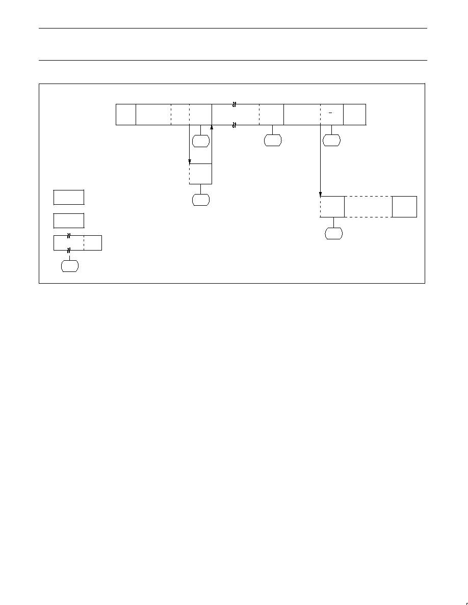
Philips Semiconductors
Product data
P83C654X2/P87C654X2
80C51 8-bit microcontroller family
16 kB OTP/ROM,
256B RAM, low voltage (2.7 to 5.5 V), low power, high speed
(30/33 MHz)
2004 Apr 20
42
««««««««
««««««««
««««««««
«««
«««
«««
«««
«««
«««
««««
««««
««««
«««
«««
«««
S
SLA
R
A
DATA
P or S
B0H
A8H
B8H
RECEPTION OF THE
OWN SLAVE ADDRESS
AND TRANSMISSION
OF ONE OR MORE
DATA BYTES
A
DATA
A
C0H
««««
««««
««
««
n
ANY NUMBER OF DATA BYTES AND THEIR ASSOCIATED ACKNOWLEDGE BITS
THIS NUMBER (CONTAINED IN S1STA) CORRESPONDS TO A DEFINED STATE OF THE I2C BUS. SEE TABLE 12.
DATA
A
«««
«««
«««
All "1"s
«««
«««
«««
A
A
««««
««««
FROM MASTER TO SLAVE
FROM SLAVE TO MASTER
C8H
P or S
LAST DATA BYTE TRANSMITTED.
SWITCHED TO NOT ADDRESSED
SLAVE (AA BIT IN S1CON = "0"
ARBITRATION LOST AS MST
AND ADDRESSED AS SLAVE
SU00974
Figure 31. Format and States of the Slave Transmitter Mode
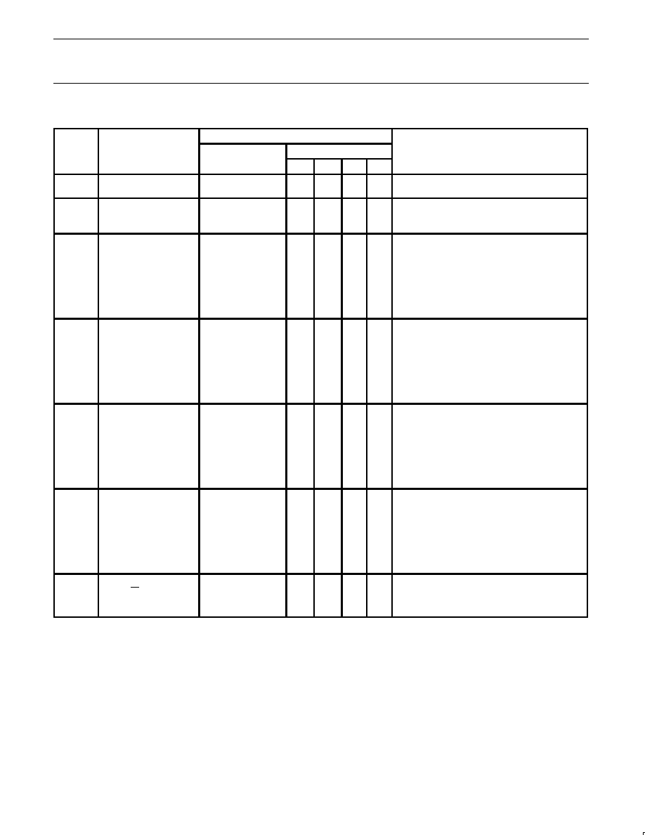
Philips Semiconductors
Product data
P83C654X2/P87C654X2
80C51 8-bit microcontroller family
16 kB OTP/ROM,
256B RAM, low voltage (2.7 to 5.5 V), low power, high speed
(30/33 MHz)
2004 Apr 20
43
Table 9.
Master Transmitter Mode
STATUS
STATUS OF THE
APPLICATION SOFTWARE RESPONSE
2
STATUS
CODE
(S1STA)
STATUS OF THE
I
2
C BUS AND
HARDWARE
TO/FROM S1DAT
TO S1CON
NEXT ACTION TAKEN BY AND I
2
C
HARDWARE
(S1STA)
HARDWARE
TO/FROM S1DAT
STA
STO
SI
AA
HARDWARE
08H
A START condition has
been transmitted
Load SLA+W
X
0
0
X
SLA+W will be transmitted;
ACK bit will be received
10H
A repeated START
diti
h
b
Load SLA+W or
X
0
0
X
As above
condition has been
transmitted
Load SLA+R
X
0
0
X
SLA+W will be transmitted;
I
2
C will be switched to MST/REC mode
18H
SLA+W has been
transmitted; ACK has
b
i
d
Load data byte or
0
0
0
X
Data byte will be transmitted;
ACK bit will be received
been received
no S1DAT action or
1
0
0
X
Repeated START will be transmitted;
no S1DAT action or
0
1
0
X
STOP condition will be transmitted;
STO flag will be reset
no S1DAT action
1
1
0
X
STOP condition followed by a
START condition will be transmitted;
STO flag will be reset
20H
SLA+W has been
transmitted; NOT ACK
h
b
i
d
Load data byte or
0
0
0
X
Data byte will be transmitted;
ACK bit will be received
has been received
no S1DAT action or
1
0
0
X
Repeated START will be transmitted;
no S1DAT action or
0
1
0
X
STOP condition will be transmitted;
STO flag will be reset
no S1DAT action
1
1
0
X
STOP condition followed by a
START condition will be transmitted;
STO flag will be reset
28H
Data byte in S1DAT has
been transmitted; ACK
h
b
i
d
Load data byte or
0
0
0
X
Data byte will be transmitted;
ACK bit will be received
has been received
no S1DAT action or
1
0
0
X
Repeated START will be transmitted;
no S1DAT action or
0
1
0
X
STOP condition will be transmitted;
STO flag will be reset
no S1DAT action
1
1
0
X
STOP condition followed by a
START condition will be transmitted;
STO flag will be reset
30H
Data byte in S1DAT has
been transmitted; NOT
ACK h
b
i
d
Load data byte or
0
0
0
X
Data byte will be transmitted;
ACK bit will be received
ACK has been received
no S1DAT action or
1
0
0
X
Repeated START will be transmitted;
no S1DAT action or
0
1
0
X
STOP condition will be transmitted;
STO flag will be reset
no S1DAT action
1
1
0
X
STOP condition followed by a
START condition will be transmitted;
STO flag will be reset
38H
Arbitration lost in
SLA+R/W or
D
b
No S1DAT action or
0
0
0
X
I
2
C-bus will be released;
not addressed slave will be entered
Data bytes
No S1DAT action
1
0
0
X
A START condition will be transmitted when the
bus becomes free

Philips Semiconductors
Product data
P83C654X2/P87C654X2
80C51 8-bit microcontroller family
16 kB OTP/ROM,
256B RAM, low voltage (2.7 to 5.5 V), low power, high speed
(30/33 MHz)
2004 Apr 20
44
Table 10.
Master Receiver Mode
STATUS
STATUS OF THE
APPLICATION SOFTWARE RESPONSE
2
STATUS
CODE
(S1STA)
STATUS OF THE
I
2
C-BUS AND
HARDWARE
TO/FROM S1DAT
TO S1CON
NEXT ACTION TAKEN BY I
2
C HARDWARE
(S1STA)
HARDWARE
TO/FROM S1DAT
STA
STO
SI
AA
08H
A START condition has
been transmitted
Load SLA+R
X
0
0
X
SLA+R will be transmitted;
ACK bit will be received
10H
A repeated START
diti
h
b
Load SLA+R or
X
0
0
X
As above
condition has been
transmitted
Load SLA+W
X
0
0
X
SLA+W will be transmitted;
I
2
C will be switched to MST/TRX mode
38H
Arbitration lost in
NOT ACK bit
No S1DAT action or
0
0
0
X
I
2
C-bus will be released;
I
2
C will enter a slave mode
No S1DAT action
1
0
0
X
A START condition will be transmitted when the
bus becomes free
40H
SLA+R has been
transmitted; ACK has
b
i
d
No S1DAT action or
0
0
0
0
Data byte will be received;
NOT ACK bit will be returned
been received
no S1DAT action
0
0
0
1
Data byte will be received;
ACK bit will be returned
48H
SLA+R has been
t
itt d NOT ACK
No S1DAT action or
1
0
0
X
Repeated START condition will be transmitted
transmitted; NOT ACK
has been received
no S1DAT action or
0
1
0
X
STOP condition will be transmitted;
STO flag will be reset
no S1DAT action
1
1
0
X
STOP condition followed by a
START condition will be transmitted;
STO flag will be reset
50H
Data byte has been
received; ACK has been
d
Read data byte or
0
0
0
0
Data byte will be received;
NOT ACK bit will be returned
returned
read data byte
0
0
0
1
Data byte will be received;
ACK bit will be returned
58H
Data byte has been
i
d NOT ACK h
Read data byte or
1
0
0
X
Repeated START condition will be transmitted
received; NOT ACK has
been returned
read data byte or
0
1
0
X
STOP condition will be transmitted;
STO flag will be reset
read data byte
1
1
0
X
STOP condition followed by a
START condition will be transmitted;
STO flag will be reset

Philips Semiconductors
Product data
P83C654X2/P87C654X2
80C51 8-bit microcontroller family
16 kB OTP/ROM,
256B RAM, low voltage (2.7 to 5.5 V), low power, high speed
(30/33 MHz)
2004 Apr 20
45
Table 11.
Slave Receiver Mode
STATUS
STATUS OF THE
APPLICATION SOFTWARE RESPONSE
2
STATUS
CODE
(S1STA)
STATUS OF THE
I
2
C BUS AND
HARDWARE
TO/FROM S1DAT
TO S1CON
NEXT ACTION TAKEN BY I
2
C HARDWARE
(S1STA)
HARDWARE
TO/FROM S1DAT
STA
STO
SI
AA
60H
Own SLA+W has
been received; ACK
h
b
d
No S1DAT action or
X
0
0
0
Data byte will be received and NOT ACK will be
returned
has been returned
no S1DAT action
X
0
0
1
Data byte will be received and ACK will be returned
68H
Arbitration lost in
SLA+R/W as master;
Own SLA+W has
b
i
d ACK
No S1DAT action or
X
0
0
0
Data byte will be received and NOT ACK will be
returned
been received, ACK
returned
no S1DAT action
X
0
0
1
Data byte will be received and ACK will be returned
70H
General call address
(00H) has been
received; ACK has
No S1DAT action or
X
0
0
0
Data byte will be received and NOT ACK will be
returned
received ACK has
been returned
no S1DAT action
X
0
0
1
Data byte will be received and ACK will be returned
78H
Arbitration lost in
SLA+R/W as master;
General call address
has been received
No S1DAT action or
X
0
0
0
Data byte will be received and NOT ACK will be
returned
has been received,
ACK has been
returned
no S1DAT action
X
0
0
1
Data byte will be received and ACK will be returned
80H
Previously addressed
with own SLV
address; DATA has
b
i
d ACK
Read data byte or
X
0
0
0
Data byte will be received and NOT ACK will be
returned
been received; ACK
has been returned
read data byte
X
0
0
1
Data byte will be received and ACK will be returned
88H
Previously addressed
with own SLA; DATA
b
h
b
Read data byte or
0
0
0
0
Switched to not addressed SLV mode; no recognition
of own SLA or General call address
byte has been
received; NOT ACK
has been returned
read data byte or
0
0
0
1
Switched to not addressed SLV mode; Own SLA will
be recognized; General call address will be
recognized if S1ADR.0 = logic 1
read data byte or
1
0
0
0
Switched to not addressed SLV mode; no recognition
of own SLA or General call address. A START
condition will be transmitted when the bus becomes
free
read data byte
1
0
0
1
Switched to not addressed SLV mode; Own SLA will
be recognized; General call address will be
recognized if S1ADR.0 = logic 1. A START condition
will be transmitted when the bus becomes free.
90H
Previously addressed
with General Call;
DATA byte has been
i
d ACK h
Read data byte or
X
0
0
0
Data byte will be received and NOT ACK will be
returned
received; ACK has
been returned
read data byte
X
0
0
1
Data byte will be received and ACK will be returned
98H
Previously addressed
with General Call;
DATA b
h
b
Read data byte or
0
0
0
0
Switched to not addressed SLV mode; no recognition
of own SLA or General call address
DATA byte has been
received; NOT ACK
has been returned
read data byte or
0
0
0
1
Switched to not addressed SLV mode; Own SLA will
be recognized; General call address will be
recognized if S1ADR.0 = logic 1
read data byte or
1
0
0
0
Switched to not addressed SLV mode; no recognition
of own SLA or General call address. A START
condition will be transmitted when the bus becomes
free
read data byte
1
0
0
1
Switched to not addressed SLV mode; Own SLA will
be recognized; General call address will be
recognized if S1ADR.0 = logic 1. A START condition
will be transmitted when the bus becomes free.
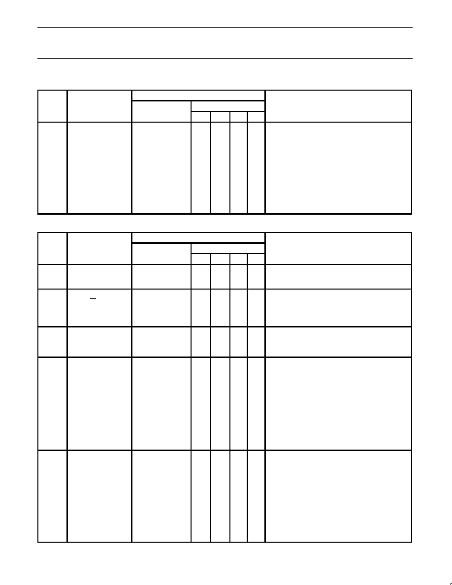
Philips Semiconductors
Product data
P83C654X2/P87C654X2
80C51 8-bit microcontroller family
16 kB OTP/ROM,
256B RAM, low voltage (2.7 to 5.5 V), low power, high speed
(30/33 MHz)
2004 Apr 20
46
Table 11.
Slave Receiver Mode (Continued)
STATUS
STATUS OF THE
APPLICATION SOFTWARE RESPONSE
2
STATUS
CODE
(S1STA)
STATUS OF THE
I
2
C BUS AND
HARDWARE
TO/FROM S1DAT
TO S1CON
NEXT ACTION TAKEN BY I
2
C HARDWARE
(S1STA)
HARDWARE
TO/FROM S1DAT
STA
STO
SI
AA
A0H
A STOP condition or
repeated START
di i
h
b
No STDAT action or
0
0
0
0
Switched to not addressed SLV mode; no recognition
of own SLA or General call address
condition has been
received while still
addressed as
SLV/REC or SLV/TRX
No STDAT action or
0
0
0
1
Switched to not addressed SLV mode; Own SLA will
be recognized; General call address will be
recognized if S1ADR.0 = logic 1
SLV/REC or SLV/TRX
No STDAT action or
1
0
0
0
Switched to not addressed SLV mode; no recognition
of own SLA or General call address. A START
condition will be transmitted when the bus becomes
free
No STDAT action
1
0
0
1
Switched to not addressed SLV mode; Own SLA will
be recognized; General call address will be
recognized if S1ADR.0 = logic 1. A START condition
will be transmitted when the bus becomes free.
Table 12.
Slave Transmitter Mode
STATUS
STATUS OF THE
APPLICATION SOFTWARE RESPONSE
2
STATUS
CODE
(S1STA)
STATUS OF THE
I
2
C BUS AND
HARDWARE
TO/FROM S1DAT
TO S1CON
NEXT ACTION TAKEN BY I
2
C HARDWARE
(S1STA)
HARDWARE
TO/FROM S1DAT
STA
STO
SI
AA
A8H
Own SLA+R has
been received; ACK
h
b
d
Load data byte or
X
0
0
0
Last data byte will be transmitted and ACK bit will be
received
has been returned
load data byte
X
0
0
1
Data byte will be transmitted; ACK will be received
B0H
Arbitration lost in
SLA+R/W as master;
Own SLA+R has
Load data byte or
X
0
0
0
Last data byte will be transmitted and ACK bit will be
received
been received, ACK
has been returned
load data byte
X
0
0
1
Data byte will be transmitted; ACK bit will be received
B8H
Data byte in S1DAT
has been transmitted;
ACK has been
Load data byte or
X
0
0
0
Last data byte will be transmitted and ACK bit will be
received
ACK has been
received
load data byte
X
0
0
1
Data byte will be transmitted; ACK bit will be received
C0H
Data byte in S1DAT
has been transmitted;
NOT ACK h
b
No S1DAT action or
0
0
0
01
Switched to not addressed SLV mode; no recognition
of own SLA or General call address
NOT ACK has been
received
no S1DAT action or
0
0
0
1
Switched to not addressed SLV mode; Own SLA will
be recognized; General call address will be
recognized if S1ADR.0 = logic 1
no S1DAT action or
1
0
0
0
Switched to not addressed SLV mode; no recognition
of own SLA or General call address. A START
condition will be transmitted when the bus becomes
free
no S1DAT action
1
0
0
1
Switched to not addressed SLV mode; Own SLA will
be recognized; General call address will be
recognized if S1ADR.0 = logic 1. A START condition
will be transmitted when the bus becomes free.
C8H
Last data byte in
S1DAT has been
i
d (AA
0)
No S1DAT action or
0
0
0
0
Switched to not addressed SLV mode; no recognition
of own SLA or General call address
transmitted (AA = 0);
ACK has been
received
no S1DAT action or
0
0
0
1
Switched to not addressed SLV mode; Own SLA will
be recognized; General call address will be
recognized if S1ADR.0 = logic 1
no S1DAT action or
1
0
0
0
Switched to not addressed SLV mode; no recognition
of own SLA or General call address. A START
condition will be transmitted when the bus becomes
free
no S1DAT action
1
0
0
1
Switched to not addressed SLV mode; Own SLA will
be recognized; General call address will be
recognized if S1ADR.0 = logic 1. A START condition
will be transmitted when the bus becomes free.
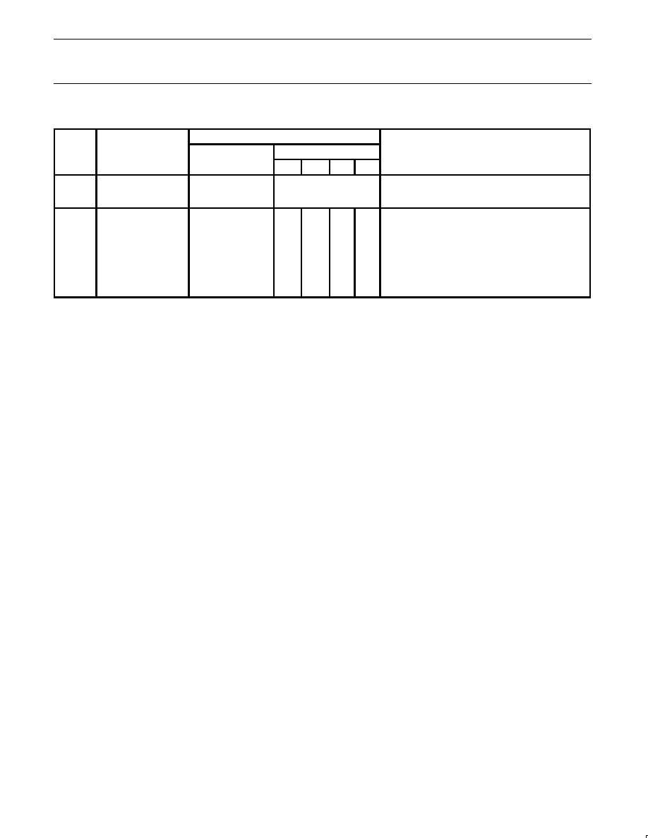
Philips Semiconductors
Product data
P83C654X2/P87C654X2
80C51 8-bit microcontroller family
16 kB OTP/ROM,
256B RAM, low voltage (2.7 to 5.5 V), low power, high speed
(30/33 MHz)
2004 Apr 20
47
Table 13.
Miscellaneous States
STATUS
STATUS OF THE
APPLICATION SOFTWARE RESPONSE
2
STATUS
CODE
(S1STA)
STATUS OF THE
I
2
C BUS AND
HARDWARE
TO/FROM S1DAT
TO S1CON
NEXT ACTION TAKEN BY I
2
C HARDWARE
(S1STA)
HARDWARE
TO/FROM S1DAT
STA
STO
SI
AA
F8H
No relevant state
information available;
SI = 0
No S1DAT action
No S1CON action
Wait or proceed current transfer
00H
Bus error during MST
or selected slave
modes, due to an
illegal START or
STOP condition. State
00H can also occur
when interference
causes I
2
C to enter
an undefined state.
No S1DAT action
0
1
0
X
Only the internal hardware is affected in the MST or
addressed SLV modes. In all cases, the bus is
released and I
2
C is switched to the not addressed
SLV mode. STO is reset.
Slave Transmitter Mode: In the slave transmitter mode, a number
of data bytes are transmitted to a master receiver (see Figure 31).
Data transfer is initialized as in the slave receiver mode. When
S1ADR and S1CON have been initialized, I
2
C waits until it is
addressed by its own slave address followed by the data direction
bit which must be logic 1 (R) for the I
2
C to operate in the slave
transmitter mode. After its own slave address and the R bit have
been received, the serial interrupt flag (SI) is set and a valid status
code can be read from S1STA. This status code is used to vector to
an interrupt service routine, and the appropriate action to be taken
for each of these status codes is detailed in Table 12. The slave
transmitter mode may also be entered if arbitration is lost while I
2
C
is in the master mode (see state B0H).
If the AA bit is reset during a transfer, I
2
C will transmit the last byte
of the transfer and enter state C0H or C8H. I
2
C is switched to the
not addressed slave mode and will ignore the master receiver if it
continues the transfer. Thus the master receiver receives all 1s as
serial data. While AA is reset, I
2
C does not respond to its own slave
address or a general call address. However, the I
2
C-bus is still
monitored, and address recognition may be resumed at any time by
setting AA. This means that the AA bit may be used to temporarily
isolate I
2
C from the I
2
C-bus.
Miscellaneous States: There are two S1STA codes that do not
correspond to a defined I
2
C hardware state (see Table 13). These
are discussed below.
S1STA = F8H:
This status code indicates that no relevant information is available
because the serial interrupt flag, SI, is not yet set. This occurs
between other states and when I
2
C is not involved in a serial
transfer.
S1STA = 00H:
This status code indicates that a bus error has occurred during an
I
2
C serial transfer. A bus error is caused when a START or STOP
condition occurs at an illegal position in the format frame. Examples
of such illegal positions are during the serial transfer of an address
byte, a data byte, or an acknowledge bit. A bus error may also be
caused when external interference disturbs the internal I
2
C signals.
When a bus error occurs, SI is set. To recover from a bus error, the
STO flag must be set and SI must be cleared. This causes I
2
C to
enter the "not addressed" slave mode (a defined state) and to clear
the STO flag (no other bits in S1CON are affected). The SDA and
SCL lines are released (a STOP condition is not transmitted).
Some Special Cases: The I
2
C hardware has facilities to handle the
following special cases that may occur during a serial transfer:
Simultaneous Repeated START Conditions from Two Masters
A repeated START condition may be generated in the master
transmitter or master receiver modes. A special case occurs if
another master simultaneously generates a repeated START
condition (see Figure 32). Until this occurs, arbitration is not lost by
either master since they were both transmitting the same data.
If the I
2
C hardware detects a repeated START condition on the
I
2
C-bus before generating a repeated START condition itself, it will
release the bus, and no interrupt request is generated. If another
master frees the bus by generating a STOP condition, I
2
C will
transmit a normal START condition (state 08H), and a retry of the
total serial data transfer can commence.
D
ATA
T
RANSFER
A
FTER
L
OSS
OF
A
RBITRATION
Arbitration may be lost in the master transmitter and master receiver
modes (see Figure 24). Loss of arbitration is indicated by the
following states in S1STA; 38H, 68H, 78H, and B0H (see Figures 28
and 29).
If the STA flag in S1CON is set by the routines which service these
states, then, if the bus is free again, a START condition (state 08H)
is transmitted without intervention by the CPU, and a retry of the
total serial transfer can commence.
F
ORCED
A
CCESS
TO
THE
I
2
C
-BUS
In some applications, it may be possible for an uncontrolled source
to cause a bus hang-up. In such situations, the problem may be
caused by interference, temporary interruption of the bus or a
temporary short-circuit between SDA and SCL.
If an uncontrolled source generates a superfluous START or masks
a STOP condition, then the I
2
C-bus stays busy indefinitely. If the
STA flag is set and bus access is not obtained within a reasonable
amount of time, then a forced access to the I
2
C-bus is possible. This
is achieved by setting the STO flag while the STA flag is still set. No
STOP condition is transmitted. The I
2
C hardware behaves as if a
STOP condition was received and is able to transmit a START
condition. The STO flag is cleared by hardware (see Figure 33).

Philips Semiconductors
Product data
P83C654X2/P87C654X2
80C51 8-bit microcontroller family
16 kB OTP/ROM,
256B RAM, low voltage (2.7 to 5.5 V), low power, high speed
(30/33 MHz)
2004 Apr 20
48
S
08H
SLA
W
A
DATA
A
S
BOTH MASTERS CONTINUE
WITH SLA TRANSMISSION
18H
28H
OTHER MASTER SENDS REPEATED
START CONDITION EARLIER
SU00975
Figure 32. Simultaneous Repeated START Conditions from 2 Masters
STA FLAG
TIME OUT
SDA LINE
SCL LINE
START CONDITION
SU00976
Figure 33. Forced Access to a Busy I
2
C-bus
I
2
C
-BUS
O
BSTRUCTED
BY
A
L
OW
L
EVEL
ON
SCL
OR
SDA
An I
2
C-bus hang-up occurs if SDA or SCL is pulled LOW by an
uncontrolled source. If the SCL line is obstructed (pulled LOW) by a
device on the bus, no further serial transfer is possible, and the I
2
C
hardware cannot resolve this type of problem. When this occurs, the
problem must be resolved by the device that is pulling the SCL bus
line LOW.
If the SDA line is obstructed by another device on the bus (e.g., a
slave device out of bit synchronization), the problem can be solved
by transmitting additional clock pulses on the SCL line (see Figure
34). The I
2
C hardware transmits additional clock pulses when the
STA flag is set, but no START condition can be generated because
the SDA line is pulled LOW while the I
2
C-bus is considered free.
The I
2
C hardware attempts to generate a START condition after
every two additional clock pulses on the SCL line. When the SDA
line is eventually released, a normal START condition is transmitted,
state 08H is entered, and the serial transfer continues.
If a forced bus access occurs or a repeated START condition is
transmitted while SDA is obstructed (pulled LOW), the I
2
C hardware
performs the same action as described above. In each case, state
08H is entered after a successful START condition is transmitted
and normal serial transfer continues. Note that the CPU is not
involved in solving these bus hang-up problems.
B
US
E
RROR
A bus error occurs when a START or STOP condition is present at
an illegal position in the format frame. Examples of illegal positions
are during the serial transfer of an address byte, a data or an
acknowledge bit.
The I
2
C hardware only reacts to a bus error when it is involved in a
serial transfer either as a master or an addressed slave. When a
bus error is detected, I
2
C immediately switches to the not addressed
slave mode, releases the SDA and SCL lines, sets the interrupt flag,
and loads the status register with 00H. This status code may be
used to vector to a service routine which either attempts the aborted
serial transfer again or simply recovers from the error condition as
shown in Table 13.

Philips Semiconductors
Product data
P83C654X2/P87C654X2
80C51 8-bit microcontroller family
16 kB OTP/ROM,
256B RAM, low voltage (2.7 to 5.5 V), low power, high speed
(30/33 MHz)
2004 Apr 20
49
STA FLAG
START CONDITION
(1) Unsuccessful attempt to send a Start condition
(2) SDA line released
(3) Successful attempt to send a Start condition; state 08H is entered
SDA LINE
SCL LINE
(1)
(1)
(2)
(3)
SU00977
Figure 34. Recovering from a Bus Obstruction Caused by a Low Level on SDA
Software Examples of I
2
C Service Routines: This section
consists of a software example for:
≠ Initialization of I
2
C after a RESET
≠ Entering the I
2
C interrupt routine
≠ The 26 state service routines for the
≠ Master transmitter mode
≠ Master receiver mode
≠ Slave receiver mode
≠ Slave transmitter mode
I
NITIALIZATION
In the initialization routine, I
2
C is enabled for both master and slave
modes. For each mode, a number of bytes of internal data RAM are
allocated to the SIO to act as either a transmission or reception
buffer. In this example, 8 bytes of internal data RAM are reserved for
different purposes. The data memory map is shown in Figure 35.
The initialization routine performs the following functions:
≠ S1ADR is loaded with the part's own slave address and the
general call bit (GC)
≠ P1.6 and P1.7 bit latches are loaded with logic 1s
≠ RAM location HADD is loaded with the high-order address byte of
the service routines
≠ The I
2
C interrupt enable and interrupt priority bits are set
≠ The slave mode is enabled by simultaneously setting the ENS1
and AA bits in S1CON and the serial clock frequency (for master
modes) is defined by loading CR0 and CR1 in S1CON. The
master routines must be started in the main program.
The I
2
C hardware now begins checking the I
2
C-bus for its own slave
address and general call. If the general call or the own slave
address is detected, an interrupt is requested and S1STA is loaded
with the appropriate state information. The following text describes a
fast method of branching to the appropriate service routine.
I
2
C I
NTERRUPT
R
OUTINE
When the I
2
C interrupt is entered, the PSW is first pushed on the
stack. Then S1STA and HADD (loaded with the high-order address
byte of the 26 service routines by the initialization routine) are
pushed on to the stack. S1STA contains a status code which is the
lower byte of one of the 26 service routines. The next instruction is
RET, which is the return from subroutine instruction. When this
instruction is executed, the HIGH and LOW order address bytes are
popped from stack and loaded into the program counter.
The next instruction to be executed is the first instruction of the state
service routine. Seven bytes of program code (which execute in
eight machine cycles) are required to branch to one of the 26 state
service routines.
SI
PUSH PSW
Save PSW
PUSH S1STA
Push status code
(low order address byte)
PUSH HADD
Push HIGH order address byte
RET
Jump to state service routine
The state service routines are located in a 256-byte page of program
memory. The location of this page is defined in the initialization
routine. The page can be located anywhere in program memory by
loading data RAM register HADD with the page number. Page 01 is
chosen in this example, and the service routines are located
between addresses 0100H and 01FFH.
T
HE
S
TATE
S
ERVICE
R
OUTINES
The state service routines are located 8 bytes from each other. Eight
bytes of code are sufficient for most of the service routines. A few of
the routines require more than 8 bytes and have to jump to other
locations to obtain more bytes of code. Each state routine is part of
the I
2
C interrupt routine and handles one of the 26 states. It ends
with a RETI instruction which causes a return to the main program.

Philips Semiconductors
Product data
P83C654X2/P87C654X2
80C51 8-bit microcontroller family
16 kB OTP/ROM,
256B RAM, low voltage (2.7 to 5.5 V), low power, high speed
(30/33 MHz)
2004 Apr 20
50
DB
S1ADR
GC
S1DAT
0
0
CR0
CR!
SI
0
AA
ST0
STA
CR2
ENS1
SPECIAL FUNCTION REGISTERS
53
BACKUP
NUMBYTMST
INTERNAL DATA RAM
S1STA
S1CON
PSW
DA
D9
D8
D0
PS1
IPO
B8
IEN0
AB
ES1
EA
P1.7
P1.6
P1
90
80
7F
ORIGINAL VALUE OF NUMBYTMST
NUMBER OF BYTES AS MASTER
52
SLA
SLA+R/W TO BE TRANSMITTED TO SLA
51
HADD
HIGHER ADDRESS BYTE INTERRUPT ROUTINE
50
SLAVE TRANSMITTER DATA RAM
4F
STD
48
SLAVE RECEIVER DATA RAM
SRD
40
MASTER RECEIVER DATA RAM
MRD
38
MASTER TRANSMITTER DATA RAM
MTD
30
19
R1
R0
18
00
SU00978
Figure 35. I
2
C Data Memory Map

Philips Semiconductors
Product data
P83C654X2/P87C654X2
80C51 8-bit microcontroller family
16 kB OTP/ROM,
256B RAM, low voltage (2.7 to 5.5 V), low power, high speed
(30/33 MHz)
2004 Apr 20
51
M
ASTER
T
RANSMITTER
AND
M
ASTER
R
ECEIVER
M
ODES
The master mode is entered in the main program. To enter the
master transmitter mode, the main program must first load the
internal data RAM with the slave address, data bytes, and the
number of data bytes to be transmitted. To enter the master receiver
mode, the main program must first load the internal data RAM with
the slave address and the number of data bytes to be received. The
R/W bit determines whether I
2
C operates in the master transmitter
or master receiver mode.
Master mode operation commences when the STA bit in S1CION is
set by the SETB instruction and data transfer is controlled by the
master state service routines in accordance with Table 9, Table 10,
Figure 28, and Figure 29. In the example below, 4 bytes are
transferred. There is no repeated START condition. In the event of
lost arbitration, the transfer is restarted when the bus becomes free.
If a bus error occurs, the I
2
C-bus is released and I
2
C enters the not
selected slave receiver mode. If a slave device returns a not
acknowledge, a STOP condition is generated.
A repeated START condition can be included in the serial transfer if
the STA flag is set instead of the STO flag in the state service
routines vectored to by status codes 28H and 58H. Additional
software must be written to determine which data is transferred after
a repeated START condition.
S
LAVE
T
RANSMITTER
AND
S
LAVE
R
ECEIVER
M
ODES
After initialization, I
2
C continually tests the I
2
C-bus and branches to
one of the slave state service routines if it detects its own slave
address or the general call address (see Table 11, Table 12, Figure
30, and Figure 31). If arbitration was lost while in the master mode,
the master mode is restarted after the current transfer. If a bus error
occurs, the I
2
C-bus is released and I
2
C enters the not selected
slave receiver mode.
In the slave receiver mode, a maximum of 8 received data bytes can
be stored in the internal data RAM. A maximum of 8 bytes ensures
that other RAM locations are not overwritten if a master sends more
bytes. If more than 8 bytes are transmitted, a not acknowledge is
returned, and I
2
C enters the not addressed slave receiver mode. A
maximum of one received data byte can be stored in the internal
data RAM after a general call address is detected. If more than one
byte is transmitted, a not acknowledge is returned and I
2
C enters
the not addressed slave receiver mode.
In the slave transmitter mode, data to be transmitted is obtained
from the same locations in the internal data RAM that were
previously loaded by the main program. After a not acknowledge
has been returned by a master receiver device, I
2
C enters the not
addressed slave mode.
A
DAPTING
THE
S
OFTWARE
FOR
D
IFFERENT
A
PPLICATIONS
The following software example shows the typical structure of the
interrupt routine including the 26 state service routines and may be
used as a base for user applications. If one or more of the four
modes are not used, the associated state service routines may be
removed but, care should be taken that a deleted routine can never
be invoked.
This example does not include any time-out routines. In the slave
modes, time-out routines are not very useful since, in these modes,
I
2
C behaves essentially as a passive device. In the master modes,
an internal timer may be used to cause a time-out if a serial transfer
is not complete after a defined period of time. This time period is
defined by the system connected to the I
2
C-bus.

Philips Semiconductors
Product data
P83C654X2/P87C654X2
80C51 8-bit microcontroller family
16 kB OTP/ROM,
256B RAM, low voltage (2.7 to 5.5 V), low power, high speed
(30/33 MHz)
2004 Apr 20
52
!********************************************************************************************************
! SI01 EQUATE LIST
!********************************************************************************************************
!********************************************************************************************************
! LOCATIONS OF THE SI01 SPECIAL FUNCTION REGISTERS
!********************************************************************************************************
00D8
S1CON
≠0xd8
00D9
S1STA
≠0xd9
00DA
S1DAT
≠0xda
00DB
S1ADR
≠0xdb
00A8
IEN0
≠0xa8
00B8
IP0
≠02b8
!********************************************************************************************************
! BIT LOCATIONS
!********************************************************************************************************
00DD
STA
≠0xdd
! STA bit in S1CON
00BD
SI01HP
≠0xbd
! IP0, SI01 Priority bit
!********************************************************************************************************
! IMMEDIATE DATA TO WRITE INTO REGISTER S1CON
!********************************************************************************************************
00D5
ENS1_NOTSTA_STO_NOTSI_AA_CR0
≠0xd5
! Generates STOP
! (CR0 = 100kHz)
00C5
ENS1_NOTSTA_NOTSTO_NOTSI_AA_CR0
≠0xc5
! Releases BUS and
! ACK
00C1
ENS1_NOTSTA_NOTSTO_NOTSI_NOTAA_CR0
≠0xc1
! Releases BUS and
! NOT ACK
00E5
ENS1_STA_NOTSTO_NOTSI_AA_CR0
≠0xe5
! Releases BUS and
! set STA
!********************************************************************************************************
! GENERAL IMMEDIATE DATA
!********************************************************************************************************
0031
OWNSLA ≠0x31
! Own SLA+General Call
! must be written into S1ADR
00A0
ENSI01
≠0xa0
! EA+ES1, enable I
2
C interrupt
! must be written into IEN0
0001
PAG1
≠0x01
! select PAG1 as HADD
00C0
SLAW
≠0xc0
! SLA+W to be transmitted
00C1
SLAR
≠0xc1
! SLA+R to be transmitted
0018
SELRB3
≠0x18
! Select Register Bank 3
!********************************************************************************************************
! LOCATIONS IN DATA RAM
!********************************************************************************************************
0030
MTD
≠0x30
! MST/TRX/DATA base address
0038
MRD
≠0x38
! MST/REC/DATA base address
0040
SRD
≠0x40
! SLV/REC/DATA base address
0048
STD
≠0x48
! SLV/TRX/DATA base address
0053
BACKUP
≠0x53
! Backup from NUMBYTMST
! To restore NUMBYTMST in case
! of an Arbitration Loss.
0052
NUMBYTMST
≠0x52
! Number of bytes to transmit
! or receive as MST.
0051
SLA
≠0x51
! Contains SLA+R/W to be
! transmitted.
0050
HADD
≠0x50
! High Address byte for STATE 0
! till STATE 25.

Philips Semiconductors
Product data
P83C654X2/P87C654X2
80C51 8-bit microcontroller family
16 kB OTP/ROM,
256B RAM, low voltage (2.7 to 5.5 V), low power, high speed
(30/33 MHz)
2004 Apr 20
53
!********************************************************************************************************
! INITIALIZATION ROUTINE
! Example to initialize IIC Interface as slave receiver or slave transmitter and
! start a MASTER TRANSMIT or a MASTER RECEIVE function. 4 bytes will be transmitted or received.
!********************************************************************************************************
.sect
strt
.base
0x00
0000
4100
ajmp INIT
! RESET
.sect
initial
.base
0x200
0200
75DB31
INIT:
mov
S1ADR,#OWNSLA
! Load own SLA + enable
! general call recognition
0203
D296
setb
P1(6)
! P1.6 High level.
0205
D297
setb
P1(7)
! P1.7 High level.
0207
755001
mov
HADD,#PAG1
020A
43A8A0
orl
IEN0,#ENSI01
! Enable SI01 interrupt
020D
C2BD
clr
SI01HP
! SI01 interrupt low priority
020F
75D8C5
mov
S1CON, #ENS1_NOTSTA_NOTSTO_NOTSI_AA_CR0
! Initialize SLV funct.
!********************************************************************************************************
!≠ ≠ ≠ ≠ ≠ ≠ ≠ ≠ ≠ ≠ ≠ ≠ ≠ ≠ ≠ ≠ ≠ ≠ ≠ ≠ ≠ ≠ ≠ ≠ ≠ ≠ ≠ ≠ ≠ ≠ ≠ ≠ ≠ ≠ ≠ ≠ ≠ ≠ ≠ ≠ ≠ ≠ ≠ ≠ ≠ ≠ ≠ ≠ ≠
! START MASTER TRANSMIT FUNCTION
!≠ ≠ ≠ ≠ ≠ ≠ ≠ ≠ ≠ ≠ ≠ ≠ ≠ ≠ ≠ ≠ ≠ ≠ ≠ ≠ ≠ ≠ ≠ ≠ ≠ ≠ ≠ ≠ ≠ ≠ ≠ ≠ ≠ ≠ ≠ ≠ ≠ ≠ ≠ ≠ ≠ ≠ ≠ ≠ ≠ ≠ ≠ ≠ ≠
0212
755204
mov
NUMBYTMST,#0x4
! Transmit 4 bytes.
0215
7551C0
mov
SLA,#SLAW
! SLA+W, Transmit funct.
0218
D2DD
setb
STA
! set STA in S1CON
!≠ ≠ ≠ ≠ ≠ ≠ ≠ ≠ ≠ ≠ ≠ ≠ ≠ ≠ ≠ ≠ ≠ ≠ ≠ ≠ ≠ ≠ ≠ ≠ ≠ ≠ ≠ ≠ ≠ ≠ ≠ ≠ ≠ ≠ ≠ ≠ ≠ ≠ ≠ ≠ ≠ ≠ ≠ ≠ ≠ ≠ ≠ ≠ ≠
! START MASTER RECEIVE FUNCTION
!≠ ≠ ≠ ≠ ≠ ≠ ≠ ≠ ≠ ≠ ≠ ≠ ≠ ≠ ≠ ≠ ≠ ≠ ≠ ≠ ≠ ≠ ≠ ≠ ≠ ≠ ≠ ≠ ≠ ≠ ≠ ≠ ≠ ≠ ≠ ≠ ≠ ≠ ≠ ≠ ≠ ≠ ≠ ≠ ≠ ≠ ≠ ≠ ≠
021A
755204
mov
NUMBYTMST,#0x4
! Receive 4 bytes.
021D
7551C1
mov
SLA,#SLAR
! SLA+R, Receive funct.
0220
D2DD
setb
STA
! set STA in S1CON
!********************************************************************************************************
! SI01 INTERRUPT ROUTINE
!********************************************************************************************************
.sect
intvec
! SI01 interrupt vector
.base
0x00
! S1STA and HADD are pushed onto the stack.
! They serve as return address for the RET instruction.
! The RET instruction sets the Program Counter to address HADD,
! S1STA and jumps to the right subroutine.
002B
C0D0
push psw
! save psw
002D
C0D9
push S1STA
002F
C050
push HADD
0031
22
ret
! JMP to address HADD,S1STA.
!≠ ≠ ≠ ≠ ≠ ≠ ≠ ≠ ≠ ≠ ≠ ≠ ≠ ≠ ≠ ≠ ≠ ≠ ≠ ≠ ≠ ≠ ≠ ≠ ≠ ≠ ≠ ≠ ≠ ≠ ≠ ≠ ≠ ≠ ≠ ≠ ≠ ≠ ≠ ≠ ≠ ≠ ≠ ≠ ≠ ≠ ≠ ≠ ≠
! STATE
: 00, Bus error.
! ACTION : Enter not addressed SLV mode and release bus. STO reset.
!≠ ≠ ≠ ≠ ≠ ≠ ≠ ≠ ≠ ≠ ≠ ≠ ≠ ≠ ≠ ≠ ≠ ≠ ≠ ≠ ≠ ≠ ≠ ≠ ≠ ≠ ≠ ≠ ≠ ≠ ≠ ≠ ≠ ≠ ≠ ≠ ≠ ≠ ≠ ≠ ≠ ≠ ≠ ≠ ≠ ≠ ≠ ≠ ≠
.sect
st0
.base
0x100
0100
75D8D5
mov
S1CON,#ENS1_NOTSTA_STO_NOTSI_AA_CR0 ! clr SI
! set STO,AA
0103
D0D0
pop
psw
0105
32
reti

Philips Semiconductors
Product data
P83C654X2/P87C654X2
80C51 8-bit microcontroller family
16 kB OTP/ROM,
256B RAM, low voltage (2.7 to 5.5 V), low power, high speed
(30/33 MHz)
2004 Apr 20
54
!********************************************************************************************************
!********************************************************************************************************
! MASTER STATE SERVICE ROUTINES
!********************************************************************************************************
! State 08 and State 10 are both for MST/TRX and MST/REC.
! The R/W bit decides whether the next state is within
! MST/TRX mode or within MST/REC mode.
!********************************************************************************************************
!≠ ≠ ≠ ≠ ≠ ≠ ≠ ≠ ≠ ≠ ≠ ≠ ≠ ≠ ≠ ≠ ≠ ≠ ≠ ≠ ≠ ≠ ≠ ≠ ≠ ≠ ≠ ≠ ≠ ≠ ≠ ≠ ≠ ≠ ≠ ≠ ≠ ≠ ≠ ≠ ≠ ≠ ≠ ≠ ≠ ≠ ≠ ≠ ≠
! STATE
: 08, A, START condition has been transmitted.
! ACTION : SLA+R/W are transmitted, ACK bit is received.
!≠ ≠ ≠ ≠ ≠ ≠ ≠ ≠ ≠ ≠ ≠ ≠ ≠ ≠ ≠ ≠ ≠ ≠ ≠ ≠ ≠ ≠ ≠ ≠ ≠ ≠ ≠ ≠ ≠ ≠ ≠ ≠ ≠ ≠ ≠ ≠ ≠ ≠ ≠ ≠ ≠ ≠ ≠ ≠ ≠ ≠ ≠ ≠ ≠
.sect
mts8
.base
0x108
0108
8551DA
mov
S1DAT,SLA
! Load SLA+R/W
010B
75D8C5
mov
S1CON,#ENS1_NOTSTA_NOTSTO_NOTSI_AA_CR0
! clr SI
010E
01A0
ajmp INITBASE1
!≠ ≠ ≠ ≠ ≠ ≠ ≠ ≠ ≠ ≠ ≠ ≠ ≠ ≠ ≠ ≠ ≠ ≠ ≠ ≠ ≠ ≠ ≠ ≠ ≠ ≠ ≠ ≠ ≠ ≠ ≠ ≠ ≠ ≠ ≠ ≠ ≠ ≠ ≠ ≠ ≠ ≠ ≠ ≠ ≠ ≠ ≠ ≠ ≠
! STATE
: 10, A repeated START condition has been
!
transmitted.
! ACTION : SLA+R/W are transmitted, ACK bit is received.
!≠ ≠ ≠ ≠ ≠ ≠ ≠ ≠ ≠ ≠ ≠ ≠ ≠ ≠ ≠ ≠ ≠ ≠ ≠ ≠ ≠ ≠ ≠ ≠ ≠ ≠ ≠ ≠ ≠ ≠ ≠ ≠ ≠ ≠ ≠ ≠ ≠ ≠ ≠ ≠ ≠ ≠ ≠ ≠ ≠ ≠ ≠ ≠ ≠
.sect
mts10
.base
0x110
0110
8551DA
mov
S1DAT,SLA
! Load SLA+R/W
0113
75D8C5
mov
S1CON,#ENS1_NOTSTA_NOTSTO_NOTSI_AA_CR0
! clr SI
010E
01A0
ajmp INITBASE1
.sect
ibase1
.base
0xa0
00A0
75D018
INITBASE1:
mov
psw,#SELRB3
00A3
7930
mov
r1,#MTD
00A5
7838
mov
r0,#MRD
00A7
855253
mov
BACKUP,NUMBYTMST
! Save initial value
00AA
D0D0
pop
psw
00AC
32
reti
!********************************************************************************************************
!********************************************************************************************************
! MASTER TRANSMITTER STATE SERVICE ROUTINES
!********************************************************************************************************
!********************************************************************************************************
!≠ ≠ ≠ ≠ ≠ ≠ ≠ ≠ ≠ ≠ ≠ ≠ ≠ ≠ ≠ ≠ ≠ ≠ ≠ ≠ ≠ ≠ ≠ ≠ ≠ ≠ ≠ ≠ ≠ ≠ ≠ ≠ ≠ ≠ ≠ ≠ ≠ ≠ ≠ ≠ ≠ ≠ ≠ ≠ ≠ ≠ ≠ ≠ ≠
! STATE
: 18, Previous state was STATE 8 or STATE 10, SLA+W have been transmitted,
!
ACK has been received.
! ACTION : First DATA is transmitted, ACK bit is received.
!≠ ≠ ≠ ≠ ≠ ≠ ≠ ≠ ≠ ≠ ≠ ≠ ≠ ≠ ≠ ≠ ≠ ≠ ≠ ≠ ≠ ≠ ≠ ≠ ≠ ≠ ≠ ≠ ≠ ≠ ≠ ≠ ≠ ≠ ≠ ≠ ≠ ≠ ≠ ≠ ≠ ≠ ≠ ≠ ≠ ≠ ≠ ≠ ≠
.sect
mts18
.base
0x118
0118
75D018
mov
psw,#SELRB3
011B
87DA
mov
S1DAT,@r1
011D
01B5
ajmp CON

Philips Semiconductors
Product data
P83C654X2/P87C654X2
80C51 8-bit microcontroller family
16 kB OTP/ROM,
256B RAM, low voltage (2.7 to 5.5 V), low power, high speed
(30/33 MHz)
2004 Apr 20
55
!≠ ≠ ≠ ≠ ≠ ≠ ≠ ≠ ≠ ≠ ≠ ≠ ≠ ≠ ≠ ≠ ≠ ≠ ≠ ≠ ≠ ≠ ≠ ≠ ≠ ≠ ≠ ≠ ≠ ≠ ≠ ≠ ≠ ≠ ≠ ≠ ≠ ≠ ≠ ≠ ≠ ≠ ≠ ≠ ≠ ≠ ≠ ≠ ≠
! STATE
: 20, SLA+W have been transmitted, NOT ACK has been received
! ACTION : Transmit STOP condition.
!≠ ≠ ≠ ≠ ≠ ≠ ≠ ≠ ≠ ≠ ≠ ≠ ≠ ≠ ≠ ≠ ≠ ≠ ≠ ≠ ≠ ≠ ≠ ≠ ≠ ≠ ≠ ≠ ≠ ≠ ≠ ≠ ≠ ≠ ≠ ≠ ≠ ≠ ≠ ≠ ≠ ≠ ≠ ≠ ≠ ≠ ≠ ≠ ≠
.sect
mts20
.base
0x120
0120
75D8D5
mov
S1CON,#ENS1_NOTSTA_STO_NOTSI_AA_CR0
! set STO, clr SI
0123
D0D0
pop
psw
0125
32
reti
!≠ ≠ ≠ ≠ ≠ ≠ ≠ ≠ ≠ ≠ ≠ ≠ ≠ ≠ ≠ ≠ ≠ ≠ ≠ ≠ ≠ ≠ ≠ ≠ ≠ ≠ ≠ ≠ ≠ ≠ ≠ ≠ ≠ ≠ ≠ ≠ ≠ ≠ ≠ ≠ ≠ ≠ ≠ ≠ ≠ ≠ ≠ ≠ ≠
! STATE
: 28, DATA of S1DAT have been transmitted, ACK received.
! ACTION : If Transmitted DATA is last DATA then transmit a STOP condition,
!
else transmit next DATA.
!≠ ≠ ≠ ≠ ≠ ≠ ≠ ≠ ≠ ≠ ≠ ≠ ≠ ≠ ≠ ≠ ≠ ≠ ≠ ≠ ≠ ≠ ≠ ≠ ≠ ≠ ≠ ≠ ≠ ≠ ≠ ≠ ≠ ≠ ≠ ≠ ≠ ≠ ≠ ≠ ≠ ≠ ≠ ≠ ≠ ≠ ≠ ≠ ≠
.sect
mts28
.base
0x128
0128
D55285
djnz
NUMBYTMST,NOTLDAT1
! JMP if NOT last DATA
012B
75D8D5
mov
S1CON,#ENS1_NOTSTA_STO_NOTSI_AA_CR0
! clr SI, set AA
012E
01B9
ajmp RETmt
.sect
mts28sb
.base
0x0b0
00B0
75D018
NOTLDAT1:
mov
psw,#SELRB3
00B3
87DA
mov
S1DAT,@r1
00B5
75D8C5
CON:
mov
S1CON,#ENS1_NOTSTA_NOTSTO_NOTSI_AA_CR0
! clr SI, set AA
00B8
09
inc
r1
00B9
D0D0
RETmt :
pop
psw
00BB
32
reti
!≠ ≠ ≠ ≠ ≠ ≠ ≠ ≠ ≠ ≠ ≠ ≠ ≠ ≠ ≠ ≠ ≠ ≠ ≠ ≠ ≠ ≠ ≠ ≠ ≠ ≠ ≠ ≠ ≠ ≠ ≠ ≠ ≠ ≠ ≠ ≠ ≠ ≠ ≠ ≠ ≠ ≠ ≠ ≠ ≠ ≠ ≠ ≠ ≠
! STATE
: 30, DATA of S1DAT have been transmitted, NOT ACK received.
! ACTION : Transmit a STOP condition.
!≠ ≠ ≠ ≠ ≠ ≠ ≠ ≠ ≠ ≠ ≠ ≠ ≠ ≠ ≠ ≠ ≠ ≠ ≠ ≠ ≠ ≠ ≠ ≠ ≠ ≠ ≠ ≠ ≠ ≠ ≠ ≠ ≠ ≠ ≠ ≠ ≠ ≠ ≠ ≠ ≠ ≠ ≠ ≠ ≠ ≠ ≠ ≠ ≠
.sect
mts30
.base
0x130
0130
75D8D5
mov
S1CON,#ENS1_NOTSTA_STO_NOTSI_AA_CR0
! set STO, clr SI
0133
D0D0
pop
psw
0135
32
reti
!≠ ≠ ≠ ≠ ≠ ≠ ≠ ≠ ≠ ≠ ≠ ≠ ≠ ≠ ≠ ≠ ≠ ≠ ≠ ≠ ≠ ≠ ≠ ≠ ≠ ≠ ≠ ≠ ≠ ≠ ≠ ≠ ≠ ≠ ≠ ≠ ≠ ≠ ≠ ≠ ≠ ≠ ≠ ≠ ≠ ≠ ≠ ≠ ≠
! STATE
: 38, Arbitration lost in SLA+W or DATA.
! ACTION : Bus is released, not addressed SLV mode is entered.
!
A new START condition is transmitted when the IIC-bus is free again.
!≠ ≠ ≠ ≠ ≠ ≠ ≠ ≠ ≠ ≠ ≠ ≠ ≠ ≠ ≠ ≠ ≠ ≠ ≠ ≠ ≠ ≠ ≠ ≠ ≠ ≠ ≠ ≠ ≠ ≠ ≠ ≠ ≠ ≠ ≠ ≠ ≠ ≠ ≠ ≠ ≠ ≠ ≠ ≠ ≠ ≠ ≠ ≠ ≠
.sect
mts38
.base
0x138
0138
75D8E5
mov
S1CON,#ENS1_STA_NOTSTO_NOTSI_AA_CR0
013B
855352
mov
NUMBYTMST,BACKUP
013E
01B9
ajmp RETmt

Philips Semiconductors
Product data
P83C654X2/P87C654X2
80C51 8-bit microcontroller family
16 kB OTP/ROM,
256B RAM, low voltage (2.7 to 5.5 V), low power, high speed
(30/33 MHz)
2004 Apr 20
56
!********************************************************************************************************
!********************************************************************************************************
! MASTER RECEIVER STATE SERVICE ROUTINES
!********************************************************************************************************
!********************************************************************************************************
!≠ ≠ ≠ ≠ ≠ ≠ ≠ ≠ ≠ ≠ ≠ ≠ ≠ ≠ ≠ ≠ ≠ ≠ ≠ ≠ ≠ ≠ ≠ ≠ ≠ ≠ ≠ ≠ ≠ ≠ ≠ ≠ ≠ ≠ ≠ ≠ ≠ ≠ ≠ ≠ ≠ ≠ ≠ ≠ ≠ ≠ ≠ ≠ ≠
! STATE
: 40, Previous state was STATE 08 or STATE 10,
!
SLA+R have been transmitted, ACK received.
! ACTION : DATA will be received, ACK returned.
!≠ ≠ ≠ ≠ ≠ ≠ ≠ ≠ ≠ ≠ ≠ ≠ ≠ ≠ ≠ ≠ ≠ ≠ ≠ ≠ ≠ ≠ ≠ ≠ ≠ ≠ ≠ ≠ ≠ ≠ ≠ ≠ ≠ ≠ ≠ ≠ ≠ ≠ ≠ ≠ ≠ ≠ ≠ ≠ ≠ ≠ ≠ ≠ ≠
.sect
mts40
.base
0x140
0140
75D8C5
mov
S1CON,#ENS1_NOTSTA_NOTSTO_NOTSI_AA_CR0
! clr STA, STO, SI set AA
0143
D0D0
pop
psw
32
reti
!≠ ≠ ≠ ≠ ≠ ≠ ≠ ≠ ≠ ≠ ≠ ≠ ≠ ≠ ≠ ≠ ≠ ≠ ≠ ≠ ≠ ≠ ≠ ≠ ≠ ≠ ≠ ≠ ≠ ≠ ≠ ≠ ≠ ≠ ≠ ≠ ≠ ≠ ≠ ≠ ≠ ≠ ≠ ≠ ≠ ≠ ≠ ≠ ≠
! STATE
: 48, SLA+R have been transmitted, NOT ACK received.
! ACTION : STOP condition will be generated.
!≠ ≠ ≠ ≠ ≠ ≠ ≠ ≠ ≠ ≠ ≠ ≠ ≠ ≠ ≠ ≠ ≠ ≠ ≠ ≠ ≠ ≠ ≠ ≠ ≠ ≠ ≠ ≠ ≠ ≠ ≠ ≠ ≠ ≠ ≠ ≠ ≠ ≠ ≠ ≠ ≠ ≠ ≠ ≠ ≠ ≠ ≠ ≠ ≠
.sect
mts48
.base
0x148
0148
75D8D5
STOP:
mov
S1CON,#ENS1_NOTSTA_STO_NOTSI_AA_CR0
! set STO, clr SI
014B
D0D0
pop
psw
014D
32
reti
!≠ ≠ ≠ ≠ ≠ ≠ ≠ ≠ ≠ ≠ ≠ ≠ ≠ ≠ ≠ ≠ ≠ ≠ ≠ ≠ ≠ ≠ ≠ ≠ ≠ ≠ ≠ ≠ ≠ ≠ ≠ ≠ ≠ ≠ ≠ ≠ ≠ ≠ ≠ ≠ ≠ ≠ ≠ ≠ ≠ ≠ ≠ ≠ ≠
! STATE
: 50, DATA have been received, ACK returned.
! ACTION : Read DATA of S1DAT.
!
DATA will be received, if it is last DATA
then NOT ACK will be returned else ACK will be returned.
!≠ ≠ ≠ ≠ ≠ ≠ ≠ ≠ ≠ ≠ ≠ ≠ ≠ ≠ ≠ ≠ ≠ ≠ ≠ ≠ ≠ ≠ ≠ ≠ ≠ ≠ ≠ ≠ ≠ ≠ ≠ ≠ ≠ ≠ ≠ ≠ ≠ ≠ ≠ ≠ ≠ ≠ ≠ ≠ ≠ ≠ ≠ ≠ ≠
.sect
mrs50
.base
0x150
0150
75D018
mov
psw,#SELRB3
0153
A6DA
mov
@r0,S1DAT
! Read received DATA
0155
01C0
ajmp REC1
.sect
mrs50s
.base
0xc0
00C0
D55205
REC1:
djnz
NUMBYTMST,NOTLDAT2
00C3
75D8C1
mov
S1CON,#ENS1_NOTSTA_NOTSTO_NOTSI_NOTAA_CR0
! clr SI,AA
00C6
8003
sjmp RETmr
00C8
75D8C5
NOTLDAT2:
mov
S1CON,#ENS1_NOTSTA_NOTSTO_NOTSI_AA_CR0
! clr SI, set AA
00CB
08
RETmr:
inc
r0
00CC
D0D0
pop
psw
00CE
32
reti
!≠ ≠ ≠ ≠ ≠ ≠ ≠ ≠ ≠ ≠ ≠ ≠ ≠ ≠ ≠ ≠ ≠ ≠ ≠ ≠ ≠ ≠ ≠ ≠ ≠ ≠ ≠ ≠ ≠ ≠ ≠ ≠ ≠ ≠ ≠ ≠ ≠ ≠ ≠ ≠ ≠ ≠ ≠ ≠ ≠ ≠ ≠ ≠ ≠
! STATE
: 58, DATA have been received, NOT ACK returned.
! ACTION : Read DATA of S1DAT and generate a STOP condition.
!≠ ≠ ≠ ≠ ≠ ≠ ≠ ≠ ≠ ≠ ≠ ≠ ≠ ≠ ≠ ≠ ≠ ≠ ≠ ≠ ≠ ≠ ≠ ≠ ≠ ≠ ≠ ≠ ≠ ≠ ≠ ≠ ≠ ≠ ≠ ≠ ≠ ≠ ≠ ≠ ≠ ≠ ≠ ≠ ≠ ≠ ≠ ≠ ≠
.sect
mrs58
.base
0x158
0158
75D018
mov
psw,#SELRB3
015B
A6DA
mov
@R0,S1DAT
015D
80E9
sjmp STOP

Philips Semiconductors
Product data
P83C654X2/P87C654X2
80C51 8-bit microcontroller family
16 kB OTP/ROM,
256B RAM, low voltage (2.7 to 5.5 V), low power, high speed
(30/33 MHz)
2004 Apr 20
57
!********************************************************************************************************
!********************************************************************************************************
! SLAVE RECEIVER STATE SERVICE ROUTINES
!********************************************************************************************************
!********************************************************************************************************
!≠ ≠ ≠ ≠ ≠ ≠ ≠ ≠ ≠ ≠ ≠ ≠ ≠ ≠ ≠ ≠ ≠ ≠ ≠ ≠ ≠ ≠ ≠ ≠ ≠ ≠ ≠ ≠ ≠ ≠ ≠ ≠ ≠ ≠ ≠ ≠ ≠ ≠ ≠ ≠ ≠ ≠ ≠ ≠ ≠ ≠ ≠ ≠ ≠
! STATE
: 60, Own SLA+W have been received, ACK returned.
! ACTION : DATA will be received and ACK returned.
!≠ ≠ ≠ ≠ ≠ ≠ ≠ ≠ ≠ ≠ ≠ ≠ ≠ ≠ ≠ ≠ ≠ ≠ ≠ ≠ ≠ ≠ ≠ ≠ ≠ ≠ ≠ ≠ ≠ ≠ ≠ ≠ ≠ ≠ ≠ ≠ ≠ ≠ ≠ ≠ ≠ ≠ ≠ ≠ ≠ ≠ ≠ ≠ ≠
.sect
srs60
.base
0x160
0160
75D8C5
mov
S1CON,#ENS1_NOTSTA_NOTSTO_NOTSI_AA_CR0
! clr SI, set AA
0163
75D018
mov
psw,#SELRB3
0166
01D0
ajmp INITSRD
.sect
insrd
.base
0xd0
00D0
7840
INITSRD:
mov
r0,#SRD
00D2
7908
mov
r1,#8
00D4
D0D0
pop
psw
00D6
32
reti
!≠ ≠ ≠ ≠ ≠ ≠ ≠ ≠ ≠ ≠ ≠ ≠ ≠ ≠ ≠ ≠ ≠ ≠ ≠ ≠ ≠ ≠ ≠ ≠ ≠ ≠ ≠ ≠ ≠ ≠ ≠ ≠ ≠ ≠ ≠ ≠ ≠ ≠ ≠ ≠ ≠ ≠ ≠ ≠ ≠ ≠ ≠ ≠ ≠
! STATE
: 68, Arbitration lost in SLA and R/W as MST
!
Own SLA+W have been received, ACK returned
! ACTION : DATA will be received and ACK returned.
!
STA is set to restart MST mode after the bus is free again.
!≠ ≠ ≠ ≠ ≠ ≠ ≠ ≠ ≠ ≠ ≠ ≠ ≠ ≠ ≠ ≠ ≠ ≠ ≠ ≠ ≠ ≠ ≠ ≠ ≠ ≠ ≠ ≠ ≠ ≠ ≠ ≠ ≠ ≠ ≠ ≠ ≠ ≠ ≠ ≠ ≠ ≠ ≠ ≠ ≠ ≠ ≠ ≠ ≠
.sect
srs68
.base
0x168
0168
75D8E5
mov
S1CON,#ENS1_STA_NOTSTO_NOTSI_AA_CR0
016B
75D018
mov
psw,#SELRB3
016E
01D0
ajmp INITSRD
!≠ ≠ ≠ ≠ ≠ ≠ ≠ ≠ ≠ ≠ ≠ ≠ ≠ ≠ ≠ ≠ ≠ ≠ ≠ ≠ ≠ ≠ ≠ ≠ ≠ ≠ ≠ ≠ ≠ ≠ ≠ ≠ ≠ ≠ ≠ ≠ ≠ ≠ ≠ ≠ ≠ ≠ ≠ ≠ ≠ ≠ ≠ ≠ ≠
! STATE
: 70, General call has been received, ACK returned.
! ACTION : DATA will be received and ACK returned.
!≠ ≠ ≠ ≠ ≠ ≠ ≠ ≠ ≠ ≠ ≠ ≠ ≠ ≠ ≠ ≠ ≠ ≠ ≠ ≠ ≠ ≠ ≠ ≠ ≠ ≠ ≠ ≠ ≠ ≠ ≠ ≠ ≠ ≠ ≠ ≠ ≠ ≠ ≠ ≠ ≠ ≠ ≠ ≠ ≠ ≠ ≠ ≠ ≠
.sect
srs70
.base
0x170
0170
75D8C5
mov
S1CON,#ENS1_NOTSTA_NOTSTO_NOTSI_AA_CR0
! clr SI, set AA
0173
75D018
mov
psw,#SELRB3
! Initialize SRD counter
0176
01D0
ajmp initsrd
!≠ ≠ ≠ ≠ ≠ ≠ ≠ ≠ ≠ ≠ ≠ ≠ ≠ ≠ ≠ ≠ ≠ ≠ ≠ ≠ ≠ ≠ ≠ ≠ ≠ ≠ ≠ ≠ ≠ ≠ ≠ ≠ ≠ ≠ ≠ ≠ ≠ ≠ ≠ ≠ ≠ ≠ ≠ ≠ ≠ ≠ ≠ ≠ ≠
! STATE
: 78, Arbitration lost in SLA+R/W as MST.
!
General call has been received, ACK returned.
! ACTION : DATA will be received and ACK returned.
!
STA is set to restart MST mode after the bus is free again.
!≠ ≠ ≠ ≠ ≠ ≠ ≠ ≠ ≠ ≠ ≠ ≠ ≠ ≠ ≠ ≠ ≠ ≠ ≠ ≠ ≠ ≠ ≠ ≠ ≠ ≠ ≠ ≠ ≠ ≠ ≠ ≠ ≠ ≠ ≠ ≠ ≠ ≠ ≠ ≠ ≠ ≠ ≠ ≠ ≠ ≠ ≠ ≠ ≠
.sect
srs78
.base
0x178
0178
75D8E5
mov
S1CON,#ENS1_STA_NOTSTO_NOTSI_AA_CR0
017B
75D018
mov
psw,#SELRB3
! Initialize SRD counter
017E
01D0
ajmp INITSRD

Philips Semiconductors
Product data
P83C654X2/P87C654X2
80C51 8-bit microcontroller family
16 kB OTP/ROM,
256B RAM, low voltage (2.7 to 5.5 V), low power, high speed
(30/33 MHz)
2004 Apr 20
58
!≠ ≠ ≠ ≠ ≠ ≠ ≠ ≠ ≠ ≠ ≠ ≠ ≠ ≠ ≠ ≠ ≠ ≠ ≠ ≠ ≠ ≠ ≠ ≠ ≠ ≠ ≠ ≠ ≠ ≠ ≠ ≠ ≠ ≠ ≠ ≠ ≠ ≠ ≠ ≠ ≠ ≠ ≠ ≠ ≠ ≠ ≠ ≠ ≠
! STATE
: 80, Previously addressed with own SLA. DATA received, ACK returned.
! ACTION : Read DATA.
!
IF received DATA was the last
!
THEN superfluous DATA will be received and NOT ACK returned
ELSE next DATA will be received and ACK returned.
!≠ ≠ ≠ ≠ ≠ ≠ ≠ ≠ ≠ ≠ ≠ ≠ ≠ ≠ ≠ ≠ ≠ ≠ ≠ ≠ ≠ ≠ ≠ ≠ ≠ ≠ ≠ ≠ ≠ ≠ ≠ ≠ ≠ ≠ ≠ ≠ ≠ ≠ ≠ ≠ ≠ ≠ ≠ ≠ ≠ ≠ ≠ ≠ ≠
.sect
srs80
.base
0x180
0180
75D018
mov
psw,#SELRB3
0183
A6DA
mov
@r0,S1DAT
! Read received DATA
0185
01D8
ajmp REC2
.sect
srs80s
.base
0xd8
00D8
D906
REC2:
djnz
r1,NOTLDAT3
00DA
75D8C1
LDAT:
mov
S1CON,#ENS1_NOTSTA_NOTSTO_NOTSI_NOTAA_CR0
! clr SI,AA
00DD
D0D0
pop
psw
00DF
32
reti
00E0
75D8C5
NOTLDAT3:
mov
S1CON,#ENS1_NOTSTA_NOTSTO_NOTSI_AA_CR0
! clr SI, set AA
00E3
08
inc
r0
00E4
D0D0
RETsr:
pop
psw
00E6
32
reti
!≠ ≠ ≠ ≠ ≠ ≠ ≠ ≠ ≠ ≠ ≠ ≠ ≠ ≠ ≠ ≠ ≠ ≠ ≠ ≠ ≠ ≠ ≠ ≠ ≠ ≠ ≠ ≠ ≠ ≠ ≠ ≠ ≠ ≠ ≠ ≠ ≠ ≠ ≠ ≠ ≠ ≠ ≠ ≠ ≠ ≠ ≠ ≠ ≠
! STATE
: 88, Previously addressed with own SLA. DATA received NOT ACK returned.
! ACTION : No save of DATA, Enter NOT addressed SLV mode.
!
Recognition of own SLA. General call recognized, if S1ADR. 0≠1.
!≠ ≠ ≠ ≠ ≠ ≠ ≠ ≠ ≠ ≠ ≠ ≠ ≠ ≠ ≠ ≠ ≠ ≠ ≠ ≠ ≠ ≠ ≠ ≠ ≠ ≠ ≠ ≠ ≠ ≠ ≠ ≠ ≠ ≠ ≠ ≠ ≠ ≠ ≠ ≠ ≠ ≠ ≠ ≠ ≠ ≠ ≠ ≠ ≠
.sect
srs88
.base
0x188
0188
75D8C5
mov
S1CON,#ENS1_NOTSTA_NOTSTO_NOTSI_AA_CR0
! clr SI, set AA
018B
01E4
ajmp RETsr
!≠ ≠ ≠ ≠ ≠ ≠ ≠ ≠ ≠ ≠ ≠ ≠ ≠ ≠ ≠ ≠ ≠ ≠ ≠ ≠ ≠ ≠ ≠ ≠ ≠ ≠ ≠ ≠ ≠ ≠ ≠ ≠ ≠ ≠ ≠ ≠ ≠ ≠ ≠ ≠ ≠ ≠ ≠ ≠ ≠ ≠ ≠ ≠ ≠
! STATE
: 90, Previously addressed with general call.
!
DATA has been received, ACK has been returned.
! ACTION : Read DATA.
After General call only one byte will be received with ACK
!
the second DATA will be received with NOT ACK.
!
DATA will be received and NOT ACK returned.
!≠ ≠ ≠ ≠ ≠ ≠ ≠ ≠ ≠ ≠ ≠ ≠ ≠ ≠ ≠ ≠ ≠ ≠ ≠ ≠ ≠ ≠ ≠ ≠ ≠ ≠ ≠ ≠ ≠ ≠ ≠ ≠ ≠ ≠ ≠ ≠ ≠ ≠ ≠ ≠ ≠ ≠ ≠ ≠ ≠ ≠ ≠ ≠ ≠
.sect
srs90
.base
0x190
0190
75D018
mov
psw,#SELRB3
0193
A6DA
mov
@r0,S1DAT
! Read received DATA
0195
01DA
ajmp LDAT
!≠ ≠ ≠ ≠ ≠ ≠ ≠ ≠ ≠ ≠ ≠ ≠ ≠ ≠ ≠ ≠ ≠ ≠ ≠ ≠ ≠ ≠ ≠ ≠ ≠ ≠ ≠ ≠ ≠ ≠ ≠ ≠ ≠ ≠ ≠ ≠ ≠ ≠ ≠ ≠ ≠ ≠ ≠ ≠ ≠ ≠ ≠ ≠ ≠
! STATE
: 98, Previously addressed with general call.
!
DATA has been received, NOT ACK has been returned.
! ACTION : No save of DATA, Enter NOT addressed SLV mode.
Recognition of own SLA. General call recognized, if S1ADR. 0≠1.
!≠ ≠ ≠ ≠ ≠ ≠ ≠ ≠ ≠ ≠ ≠ ≠ ≠ ≠ ≠ ≠ ≠ ≠ ≠ ≠ ≠ ≠ ≠ ≠ ≠ ≠ ≠ ≠ ≠ ≠ ≠ ≠ ≠ ≠ ≠ ≠ ≠ ≠ ≠ ≠ ≠ ≠ ≠ ≠ ≠ ≠ ≠ ≠ ≠
.sect
srs98
.base
0x198
0198
75D8C5
mov
S1CON,#ENS1_NOTSTA_NOTSTO_NOTSI_AA_CR0
! clr SI, set AA
019B
D0D0
pop
psw
019D
32
reti

Philips Semiconductors
Product data
P83C654X2/P87C654X2
80C51 8-bit microcontroller family
16 kB OTP/ROM,
256B RAM, low voltage (2.7 to 5.5 V), low power, high speed
(30/33 MHz)
2004 Apr 20
59
!≠ ≠ ≠ ≠ ≠ ≠ ≠ ≠ ≠ ≠ ≠ ≠ ≠ ≠ ≠ ≠ ≠ ≠ ≠ ≠ ≠ ≠ ≠ ≠ ≠ ≠ ≠ ≠ ≠ ≠ ≠ ≠ ≠ ≠ ≠ ≠ ≠ ≠ ≠ ≠ ≠ ≠ ≠ ≠ ≠ ≠ ≠ ≠ ≠
! STATE
: A0, A STOP condition or repeated START has been received,
!
while still addressed as SLV/REC or SLV/TRX.
! ACTION : No save of DATA, Enter NOT addressed SLV mode.
!
Recognition of own SLA. General call recognized, if S1ADR. 0≠1.
!≠ ≠ ≠ ≠ ≠ ≠ ≠ ≠ ≠ ≠ ≠ ≠ ≠ ≠ ≠ ≠ ≠ ≠ ≠ ≠ ≠ ≠ ≠ ≠ ≠ ≠ ≠ ≠ ≠ ≠ ≠ ≠ ≠ ≠ ≠ ≠ ≠ ≠ ≠ ≠ ≠ ≠ ≠ ≠ ≠ ≠ ≠ ≠ ≠
.sect
srsA0
.base
0x1a0
01A0
75D8C5
mov
S1CON,#ENS1_NOTSTA_NOTSTO_NOTSI_AA_CR0
! clr SI, set AA
01A3
D0D0
pop
psw
01A5
32
reti
!********************************************************************************************************
!********************************************************************************************************
! SLAVE TRANSMITTER STATE SERVICE ROUTINES
!********************************************************************************************************
!********************************************************************************************************
!≠ ≠ ≠ ≠ ≠ ≠ ≠ ≠ ≠ ≠ ≠ ≠ ≠ ≠ ≠ ≠ ≠ ≠ ≠ ≠ ≠ ≠ ≠ ≠ ≠ ≠ ≠ ≠ ≠ ≠ ≠ ≠ ≠ ≠ ≠ ≠ ≠ ≠ ≠ ≠ ≠ ≠ ≠ ≠ ≠ ≠ ≠ ≠ ≠
! STATE
: A8, Own SLA+R received, ACK returned.
! ACTION : DATA will be transmitted, A bit received.
!≠ ≠ ≠ ≠ ≠ ≠ ≠ ≠ ≠ ≠ ≠ ≠ ≠ ≠ ≠ ≠ ≠ ≠ ≠ ≠ ≠ ≠ ≠ ≠ ≠ ≠ ≠ ≠ ≠ ≠ ≠ ≠ ≠ ≠ ≠ ≠ ≠ ≠ ≠ ≠ ≠ ≠ ≠ ≠ ≠ ≠ ≠ ≠ ≠
.sect
stsa8
.base
0x1a8
01A8
8548DA
mov
S1DAT,STD
! load DATA in S1DAT
01AB
75D8C5
mov
S1CON,#ENS1_NOTSTA_NOTSTO_NOTSI_AA_CR0
! clr SI, set AA
01AE
01E8
ajmp INITBASE2
.sect
ibase2
.base
0xe8
00E8
75D018
INITBASE2:
mov
psw,#SELRB3
00EB
7948
mov
r1, #STD
00ED
09
inc
r1
00EE
D0D0
pop
psw
00F0
32
reti
!≠ ≠ ≠ ≠ ≠ ≠ ≠ ≠ ≠ ≠ ≠ ≠ ≠ ≠ ≠ ≠ ≠ ≠ ≠ ≠ ≠ ≠ ≠ ≠ ≠ ≠ ≠ ≠ ≠ ≠ ≠ ≠ ≠ ≠ ≠ ≠ ≠ ≠ ≠ ≠ ≠ ≠ ≠ ≠ ≠ ≠ ≠ ≠ ≠
! STATE
: B0, Arbitration lost in SLA and R/W as MST. Own SLA+R received, ACK returned.
! ACTION : DATA will be transmitted, A bit received.
!
STA is set to restart MST mode after the bus is free again.
!≠ ≠ ≠ ≠ ≠ ≠ ≠ ≠ ≠ ≠ ≠ ≠ ≠ ≠ ≠ ≠ ≠ ≠ ≠ ≠ ≠ ≠ ≠ ≠ ≠ ≠ ≠ ≠ ≠ ≠ ≠ ≠ ≠ ≠ ≠ ≠ ≠ ≠ ≠ ≠ ≠ ≠ ≠ ≠ ≠ ≠ ≠ ≠ ≠
.sect
stsb0
.base
0x1b0
01B0
8548DA
mov
S1DAT,STD
! load DATA in S1DAT
01B3
75D8E5
mov
S1CON,#ENS1_STA_NOTSTO_NOTSI_AA_CR0
01B6
01E8
ajmp INITBASE2

Philips Semiconductors
Product data
P83C654X2/P87C654X2
80C51 8-bit microcontroller family
16 kB OTP/ROM,
256B RAM, low voltage (2.7 to 5.5 V), low power, high speed
(30/33 MHz)
2004 Apr 20
60
!≠ ≠ ≠ ≠ ≠ ≠ ≠ ≠ ≠ ≠ ≠ ≠ ≠ ≠ ≠ ≠ ≠ ≠ ≠ ≠ ≠ ≠ ≠ ≠ ≠ ≠ ≠ ≠ ≠ ≠ ≠ ≠ ≠ ≠ ≠ ≠ ≠ ≠ ≠ ≠ ≠ ≠ ≠ ≠ ≠ ≠ ≠ ≠ ≠
! STATE
: B8, DATA has been transmitted, ACK received.
! ACTION : DATA will be transmitted, ACK bit is received.
!≠ ≠ ≠ ≠ ≠ ≠ ≠ ≠ ≠ ≠ ≠ ≠ ≠ ≠ ≠ ≠ ≠ ≠ ≠ ≠ ≠ ≠ ≠ ≠ ≠ ≠ ≠ ≠ ≠ ≠ ≠ ≠ ≠ ≠ ≠ ≠ ≠ ≠ ≠ ≠ ≠ ≠ ≠ ≠ ≠ ≠ ≠ ≠ ≠
.sect
stsb8
.base
0x1b8
01B8
75D018
mov
psw,#SELRB3
01BB
87DA
mov
S1DAT,@r1
01BD
01F8
ajmp SCON
.sect
scn
.base
0xf8
00F8
75D8C5
SCON:
mov
S1CON,#ENS1_NOTSTA_NOTSTO_NOTSI_AA_CR0
! clr SI, set AA
00FB
09
inc
r1
00FC
D0D0
pop
psw
00FE
32
reti
!≠ ≠ ≠ ≠ ≠ ≠ ≠ ≠ ≠ ≠ ≠ ≠ ≠ ≠ ≠ ≠ ≠ ≠ ≠ ≠ ≠ ≠ ≠ ≠ ≠ ≠ ≠ ≠ ≠ ≠ ≠ ≠ ≠ ≠ ≠ ≠ ≠ ≠ ≠ ≠ ≠ ≠ ≠ ≠ ≠ ≠ ≠ ≠ ≠
! STATE
: C0, DATA has been transmitted, NOT ACK received.
! ACTION : Enter not addressed SLV mode.
!≠ ≠ ≠ ≠ ≠ ≠ ≠ ≠ ≠ ≠ ≠ ≠ ≠ ≠ ≠ ≠ ≠ ≠ ≠ ≠ ≠ ≠ ≠ ≠ ≠ ≠ ≠ ≠ ≠ ≠ ≠ ≠ ≠ ≠ ≠ ≠ ≠ ≠ ≠ ≠ ≠ ≠ ≠ ≠ ≠ ≠ ≠ ≠ ≠
.sect
stsc0
.base
0x1c0
01C0
75D8C5
mov
S1CON,#ENS1_NOTSTA_NOTSTO_NOTSI_AA_CR0
! clr SI, set AA
01C3
D0D0
pop
psw
01C5
32
reti
!≠ ≠ ≠ ≠ ≠ ≠ ≠ ≠ ≠ ≠ ≠ ≠ ≠ ≠ ≠ ≠ ≠ ≠ ≠ ≠ ≠ ≠ ≠ ≠ ≠ ≠ ≠ ≠ ≠ ≠ ≠ ≠ ≠ ≠ ≠ ≠ ≠ ≠ ≠ ≠ ≠ ≠ ≠ ≠ ≠ ≠ ≠ ≠ ≠
! STATE
: C8, Last DATA has been transmitted (AA=0), ACK received.
! ACTION : Enter not addressed SLV mode.
!≠ ≠ ≠ ≠ ≠ ≠ ≠ ≠ ≠ ≠ ≠ ≠ ≠ ≠ ≠ ≠ ≠ ≠ ≠ ≠ ≠ ≠ ≠ ≠ ≠ ≠ ≠ ≠ ≠ ≠ ≠ ≠ ≠ ≠ ≠ ≠ ≠ ≠ ≠ ≠ ≠ ≠ ≠ ≠ ≠ ≠ ≠ ≠ ≠
.sect
stsc8
.base
0x1c8
01C8
75D8C5
mov
S1CON,#ENS1_NOTSTA_NOTSTO_NOTSI_AA_CR0
! clr SI, set AA
01CB
D0D0
pop
psw
01CD
32
reti
!********************************************************************************************************
!********************************************************************************************************
! END OF SI01 INTERRUPT ROUTINE
!********************************************************************************************************
!********************************************************************************************************

Philips Semiconductors
Product data
P83C654X2/P87C654X2
80C51 8-bit microcontroller family
16 kB OTP/ROM,
256B RAM, low voltage (2.7 to 5.5 V), low power, high speed
(30/33 MHz)
2004 Apr 20
61
Interrupt Priority Structure
The P8xC654X2 has an 8 source four-level interrupt structure (see
Table 14).
There are four SFRs associated with the four-level interrupt. They
are IE, IEN1, IP, and IPH. The IPH (Interrupt Priority High) register
makes the four-level interrupt structure possible. The IPH is located
at SFR address B7H. The structure of the IPH register and a
description of its bits is shown in Figure 38.
The function of the IPH SFR, when combined with the IP SFR,
determines the priority of each interrupt. The priority of each
interrupt is determined as shown in the following table:
PRIORITY BITS
INTERRUPT PRIORITY LEVEL
IPH.x
IP.x
INTERRUPT PRIORITY LEVEL
0
0
Level 0 (lowest priority)
0
1
Level 1
1
0
Level 2
1
1
Level 3 (highest priority)
Table 14.
Interrupt Table
SOURCE
POLLING PRIORITY
REQUEST BITS
HARDWARE CLEAR?
VECTOR ADDRESS
X0
1
IE0
N (L)
1
Y (T)
2
03H
SI01 (I2C)
2
≠
N
2BH
T0
3
TP0
Y
0BH
X1
4
IE1
N (L)
Y (T)
13H
T1
5
TF1
Y
1BH
SP
6
RI, TI
N
23H
T2
7
TF2, EXF2
N
3BH
NOTES:
1. L = Level activated
2. T = Transition activated
The priority scheme for servicing the interrupts is the same as that
for the 80C51, except there are four interrupt levels rather than two
as on the 80C51. An interrupt will be serviced as long as an interrupt
of equal or higher priority is not already being serviced. If an
interrupt of equal or higher level priority is being serviced, the new
interrupt will wait until it is finished before being serviced. If a lower
priority level interrupt is being serviced, it will be stopped and the
new interrupt serviced. When the new interrupt is finished, the lower
priority level interrupt that was stopped will be completed.
EX0
IE (0A8H)
Enable Bit = 1 enables the interrupt.
Enable Bit = 0 disables it.
BIT
SYMBOL
FUNCTION
IE.7
EA
Global disable bit. If EA = 0, all interrupts are disabled. If EA = 1, each interrupt can be individually
enabled or disabled by setting or clearing its enable bit.
IE.6
≠
≠
IE.5
ET2
Timer 2 interrupt enable bit.
IE.4
ES
Serial Port interrupt enable bit.
IE.3
ET1
Timer 1 interrupt enable bit.
IE.2
EX1
External interrupt 1 enable bit.
IE.1
ET0
Timer 0 interrupt enable bit.
IE.0
EX0
External interrupt 0 enable bit.
SU01745
ET0
EX1
ET1
ES
ET2
≠
EA
0
1
2
3
4
5
6
7
Figure 36. IE Registers

Philips Semiconductors
Product data
P83C654X2/P87C654X2
80C51 8-bit microcontroller family
16 kB OTP/ROM,
256B RAM, low voltage (2.7 to 5.5 V), low power, high speed
(30/33 MHz)
2004 Apr 20
62
PX0
IP (0B8H)
Priority Bit = 1 assigns high priority
Priority Bit = 0 assigns low priority
BIT
SYMBOL
FUNCTION
IP.7
≠
≠
IP.6
≠
≠
IP.5
PT2
Timer 2 interrupt priority bit.
IP.4
PS
Serial Port interrupt priority bit.
IP.3
PT1
Timer 1 interrupt priority bit.
IP.2
PX1
External interrupt 1 priority bit.
IP.1
PT0
Timer 0 interrupt priority bit.
IP.0
PX0
External interrupt 0 priority bit.
SU01743
PT0
PX1
PT1
PS
PT2
≠
≠
0
1
2
3
4
5
6
7
Figure 37. IP Registers
PX0H
IPH (B7H)
Priority Bit = 1 assigns higher priority
Priority Bit = 0 assigns lower priority
BIT
SYMBOL
FUNCTION
IPH.7
≠
≠
IPH.6
≠
≠
IPH.5
PT2H
Timer 2 interrupt priority bit high.
IPH.4
PSH
Serial Port interrupt priority bit high.
IPH.3
PT1H
Timer 1 interrupt priority bit high.
IPH.2
PX1H
External interrupt 1 priority bit high.
IPH.1
PT0H
Timer 0 interrupt priority bit high.
IPH.0
PX0H
External interrupt 0 priority bit high.
SU01744
PT0H
PX1H
PT1H
PSH
PT2H
≠
≠
0
1
2
3
4
5
6
7
Figure 38. IPH Registers

Philips Semiconductors
Product data
P83C654X2/P87C654X2
80C51 8-bit microcontroller family
16 kB OTP/ROM,
256B RAM, low voltage (2.7 to 5.5 V), low power, high speed
(30/33 MHz)
2004 Apr 20
63
Reduced EMI Mode
The AO bit (AUXR.0) in the AUXR register when set disables the
ALE output unless the CPU needs to perform an off-chip memory
access.
Reduced EMI Mode
AUXR (8EH)
7
6
5
4
3
2
1
0
≠
≠
≠
≠
Fast/
STD
I
2
C
≠
≠
AO
AUXR.0
AO
Dual DPTR
The dual DPTR structure (see Figure 39) is a way by which the chip
will specify the address of an external data memory location. There
are two 16-bit DPTR registers that address the external memory,
and a single bit called DPS = AUXR1/bit0 that allows the program
code to switch between them.
∑
New Register Name: AUXR1#
∑
SFR Address: A2H
∑
Reset Value: xxxxxxx0B
AUXR1 (A2H)
7
6
5
4
3
2
1
0
≠
≠
≠
LPEP
GFS
0
≠
DPS
Where:
DPS = AUXR1/bit0 = Switches between DPTR0 and DPTR1.
Select Reg
DPS
DPTR0
0
DPTR1
1
The DPS bit status should be saved by software when switching
between DPTR0 and DPTR1.
The GPS bit is a general purpose user-defined flag. Note that bit 2 is
not writable and is always read as a zero. This allows the DPS bit to
be quickly toggled simply by executing an INC AUXR1 instruction
without affecting the GPS bit.
DPS
DPTR1
DPTR0
DPH
(83H)
DPL
(82H)
EXTERNAL
DATA
MEMORY
SU00745A
BIT0
AUXR1
Figure 39.
DPTR Instructions
The instructions that refer to DPTR refer to the data pointer that is
currently selected using the AUXR1/bit 0 register. The six
instructions that use the DPTR are as follows:
INC DPTR
Increments the data pointer by 1
MOV DPTR, #data16
Loads the DPTR with a 16-bit constant
MOV A, @ A+DPTR
Move code byte relative to DPTR to ACC
MOVX A, @ DPTR
Move external RAM (16-bit address) to
ACC
MOVX @ DPTR , A
Move ACC to external RAM (16-bit
address)
JMP @ A + DPTR
Jump indirect relative to DPTR
The data pointer can be accessed on a byte-by-byte basis by
specifying the LOW or HIGH byte in an instruction which accesses
the SFRs. See
Application Note AN458 for more details.
UPPER
128 BYTES
INTERNAL RAM
LOWER
128 BYTES
INTERNAL RAM
SPECIAL
FUNCTION
REGISTER
FF
00
FF
00
80
80
EXTERNAL
DATA
MEMORY
FFFF
0000
SU01741
Figure 40. Internal and External Data Memory Address Space with EXTRAM = 0

Philips Semiconductors
Product data
P83C654X2/P87C654X2
80C51 8-bit microcontroller family
16 kB OTP/ROM,
256B RAM, low voltage (2.7 to 5.5 V), low power, high speed
(30/33 MHz)
2004 Apr 20
64
HARDWARE WATCHDOG TIMER (ONE-TIME
ENABLED WITH RESET-OUT FOR P8XC654X2)
The WDT is intended as a recovery method in situations where the
CPU may be subjected to software upset. The WDT consists of a
14-bit counter and the WatchDog Timer reset (WDTRST) SFR. The
WDT is disabled at reset.
Using the WDT
To enable the WDT, the user must write 01EH and 0E1H in sequence
to the WDTRST, SFR location 0A6H. When the WDT is enabled, the
user needs to service it by writing 01EH and 0E1H to WDTRST to
avoid a WDT overflow. The 14-bit counter overflows when it reaches
16383 (3FFFH) and this will reset the device. When the WDT is
enabled, it will increment every machine cycle while the oscillator is
running. This means the user must reset the WDT at least every
16383 machine cycles. To reset the WDT, the user must write 01EH
and 0E1H to WDTRST. WDTRST is a write only register. The WDT
counter cannot be read or written. When the WDT overflows, it will
generate an output RESET pulse at the reset pin (see note below).
The RESET pulse duration is 98
◊
T
osc
(6-clock mode; 196 in
12-clock mode), where T
osc
= 1/f
osc
. To make the best use of the
WDT, it should be serviced in those sections of code that will
periodically be executed within the time required to prevent a WDT
reset.

Philips Semiconductors
Product data
P83C654X2/P87C654X2
80C51 8-bit microcontroller family
16 kB OTP/ROM,
256B RAM, low voltage (2.7 to 5.5 V), low power, high speed
(30/33 MHz)
2004 Apr 20
65
ABSOLUTE MAXIMUM RATINGS
1, 2, 3
PARAMETER
RATING
UNIT
Operating temperature under bias
0 to +70 or ≠40 to +85
∞
C
Storage temperature range
≠65 to +150
∞
C
Voltage on EA/V
PP
pin to V
SS
0 to +13.0
V
Voltage on any other pin to V
SS
4
≠0.5 to +6.0
V
Maximum I
OL
per I/O pin
15
mA
Power dissipation (based on package heat transfer limitations, not device power consumption)
1.5
W
NOTES:
1. Stresses above those listed under Absolute Maximum Ratings may cause permanent damage to the device. This is a stress rating only and
functional operation of the device at these or any conditions other than those described in the AC and DC Electrical Characteristics section
of this specification is not implied.
2. This product includes circuitry specifically designed for the protection of its internal devices from the damaging effects of excessive static
charge. Nonetheless, it is suggested that conventional precautions be taken to avoid applying greater than the rated maximum.
3. Parameters are valid over operating temperature range unless otherwise specified. All voltages are with respect to V
SS
unless otherwise
noted.
4. Transient voltage only.
AC ELECTRICAL CHARACTERISTICS
T
amb
= 0
∞
C to +70
∞
C or ≠40
∞
C to +85
∞
C
CLOCK FREQUENCY
RANGE
SYMBOL
FIGURE
PARAMETER
OPERATING MODE
POWER SUPPLY
VOLTAGE
MIN
MAX
UNIT
1/t
CLCL
46
Oscillator frequency
6-clock
5 V
"
10 %
0
30
MHz
6-clock
2.7 V to 5.5 V
0
16
MHz
12-clock
5 V
"
10 %
0
33
MHz
12-clock
2.7 V to 5.5 V
0
16
MHz
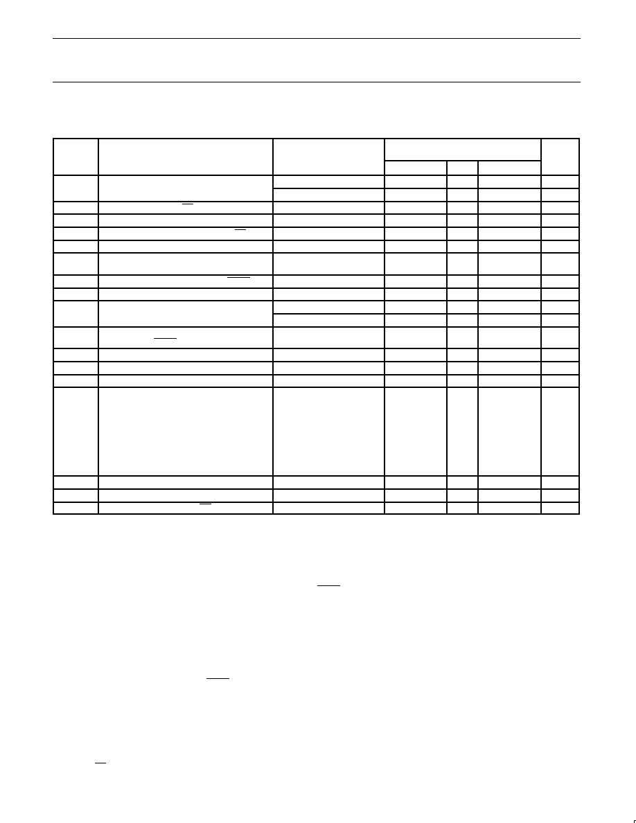
Philips Semiconductors
Product data
P83C654X2/P87C654X2
80C51 8-bit microcontroller family
16 kB OTP/ROM,
256B RAM, low voltage (2.7 to 5.5 V), low power, high speed
(30/33 MHz)
2004 Apr 20
66
DC ELECTRICAL CHARACTERISTICS
T
amb
= 0
∞
C to +70
∞
C or ≠40
∞
C to +85
∞
C; V
CC
= 2.7 V to 5.5 V; V
SS
= 0 V (16 MHz max. CPU clock)
SYMBOL
PARAMETER
TEST
CONDITIONS
LIMITS
UNIT
MIN
TYP
1
MAX
V
IL
Input LOW voltage
11
, except P1.6 and P1.7
4.0 V < V
CC
< 5.5 V
≠0.5
0.2V
CC
≠ 0.1
V
2.7 V < V
CC
< 4.0 V
≠0.5
0.7V
CC
V
V
IL1
Input LOW voltage to EA
≠0.5
0.2V
DD
≠ 0.3
V
V
IL2
Input LOW voltage to P1.6/SCL, P1.7/SDA
5
≠0.5
0.3V
DD
V
V
IH
Input HIGH voltage (ports 0, 1, 2, 3, EA)
0.2V
CC
+ 0.9
V
CC
+ 0.5
V
V
IH1
Input HIGH voltage, XTAL1, RST
11
0.7V
CC
V
CC
+ 0.5
V
V
OL
Output LOW voltage, ports 1, 2
8
, except P1.6
and P1.7
V
CC
= 2.7 V; I
OL
= 1.6 mA
2
≠
0.4
V
V
OL1
Output LOW voltage, port 0, ALE, PSEN
8, 7
V
CC
= 2.7 V; I
OL
= 3.2 mA
2
≠
0.4
V
V
OL2
Output LOW voltage, P1.6/SCL, P1.7/SDA
I
OL
= 3.0 mA
7
≠
0.4
V
V
OH
Output HIGH voltage, ports 1, 2, 3
3
V
CC
= 2.7 V; I
OH
= ≠20
m
A
V
CC
≠ 0.7
≠
V
V
CC
= 4.5 V; I
OH
= ≠30
m
A
V
CC
≠ 0.7
≠
V
V
OH1
Output HIGH voltage (port 0 in external bus
mode), ALE
9
, PSEN
3
V
CC
= 2.7 V; I
OH
= ≠3.2 mA
V
CC
≠ 0.7
≠
V
I
IL
Logical 0 input current, ports 1, 2, 3
V
IN
= 0.4 V
≠1
≠50
m
A
I
TL
Logical 1-to-0 transition current, ports 1, 2, 3
6
V
IN
= 2.0 V; See note 4
≠
≠650
m
A
I
LI
Input leakage current, port 0
0.45 < V
IN
< V
CC
≠ 0.3
≠
±
10
m
A
I
CC
Power supply current (see Figure 49 and
Source Code):
Active mode @ 16 MHz
m
A
Idle mode @ 16 MHz
m
A
Power-down mode or clock stopped
(see Figure 45 for conditions)
12
T
amb
= 0
∞
C to 70
∞
C
2
30
m
A
T
amb
= ≠40
∞
C to +85
∞
C
3
50
m
A
V
RAM
RAM keep-alive voltage
1.2
V
R
RST
Internal reset pull-down resistor
40
225
k
C
IO
Pin capacitance
10
(except EA)
≠
15
pF
NOTES:
1. Typical ratings are not guaranteed. Values listed are based on tests conducted on limited number of samples at room temperature.
2. Capacitive loading on ports 0 and 2 may cause spurious noise to be superimposed on the V
OL
s of ALE and ports 1 and 3. The noise is
due to external bus capacitance discharging into the port 0 and port 2 pins when these pins make 1-to-0 transitions during bus operations.
In the worst cases (capacitive loading > 100 pF), the noise pulse on the ALE pin may exceed 0.8 V. In such cases, it may be desirable to
qualify ALE with a Schmitt Trigger, or use an address latch with a Schmitt Trigger STROBE input. I
OL
can exceed these conditions provided
that no single output sinks more than 5 mA and no more than two outputs exceed the test conditions.
3. Capacitive loading on ports 0 and 2 may cause the V
OH
on ALE and PSEN to momentarily fall below the V
CC
≠0.7 specification when the
address bits are stabilizing.
4. Pins of ports 1, 2 and 3 source a transition current when they are being externally driven from 1 to 0. The transition current reaches its
maximum value when V
IN
is approximately 2 V.
5. See Figures 51 through 54 for I
CC
test conditions and Figure 49 for I
CC
vs. Frequency
12-clock mode characteristics:
Active mode (operating):
I
CC
= 1.0 mA + 1.1 mA
◊
FREQ.[MHz]
Active mode (reset):
I
CC
= 7.0 mA + 0.6 mA
FREQ.[MHz]
Idle mode:
I
CC
= 1.0 mA + 0.22 mA
FREQ.[MHz]
6. This value applies to T
amb
= 0
∞
C to +70
∞
C. For T
amb
= ≠40
∞
C to +85
∞
C, I
TL
= ≠750
m
A.
7. Load capacitance for port 0, ALE, and PSEN = 100 pF, load capacitance for all other outputs = 80 pF.
8. Under steady state (non-transient) conditions, I
OL
must be externally limited as follows:
Maximum I
OL
per port pin:
15 mA (*NOTE: This is 85
∞
C specification.)
Maximum I
OL
per 8-bit port:
26 mA
Maximum total I
OL
for all outputs:
71 mA
If I
OL
exceeds the test condition, V
OL
may exceed the related specification. Pins are not guaranteed to sink current greater than the listed
test conditions.
9. ALE is tested to V
OH1
, except when ALE is off then V
OH
is the voltage specification.
10. Pin capacitance is characterized but not tested. Pin capacitance is less than 25 pF. Pin capacitance of ceramic package is less than 15 pF
(except EA is 25 pF).

Philips Semiconductors
Product data
P83C654X2/P87C654X2
80C51 8-bit microcontroller family
16 kB OTP/ROM,
256B RAM, low voltage (2.7 to 5.5 V), low power, high speed
(30/33 MHz)
2004 Apr 20
67
11. To improve noise rejection a nominal 100 ns glitch rejection circuitry has been added to the RST pin, and a nominal 15 ns glitch rejection
circuitry has been added to the INT0 and INT1 pins. Previous devices provided only an inherent 5 ns of glitch rejection.
12. Power-down mode for 3 V range: Commercial Temperature Range ≠ typ: 0.5
m
A, max. 20
m
A; Industrial Temperature Range ≠ typ. 1.0
m
A,
max. 30
m
A;
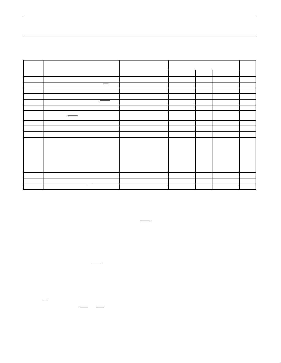
Philips Semiconductors
Product data
P83C654X2/P87C654X2
80C51 8-bit microcontroller family
16 kB OTP/ROM,
256B RAM, low voltage (2.7 to 5.5 V), low power, high speed
(30/33 MHz)
2004 Apr 20
68
DC ELECTRICAL CHARACTERISTICS
T
amb
= 0
∞
C to +70
∞
C or ≠40
∞
C to +85
∞
C; V
CC
= 5 V
±
10 %; V
SS
= 0 V (30/33 MHz max. CPU clock)
SYMBOL
PARAMETER
TEST
CONDITIONS
LIMITS
UNIT
MIN
TYP
1
MAX
V
IL
Input LOW voltage
11
4.5 V < V
CC
< 5.5 V
≠0.5
0.2V
CC
≠ 0.1
V
V
IH
Input HIGH voltage (ports 0, 1, 2, 3, EA)
0.2V
CC
+ 0.9
V
CC
+ 0.5
V
V
IH1
Input HIGH voltage, XTAL1, RST
11
0.7V
CC
V
CC
+ 0.5
V
V
OL
Output LOW voltage, ports 1, 2, 3
8
V
CC
= 4.5 V; I
OL
= 1.6 mA
2
≠
0.4
V
V
OL1
Output LOW voltage, port 0, ALE, PSEN
7, 8
V
CC
= 4.5 V; I
OL
= 3.2 mA
2
≠
0.4
V
V
OH
Output HIGH voltage, ports 1, 2, 3
3
V
CC
= 4.5 V; I
OH
= ≠30
m
A
V
CC
≠ 0.7
≠
V
V
OH1
Output HIGH voltage (port 0 in external bus
mode), ALE
9
, PSEN
3
V
CC
= 4.5 V; I
OH
= ≠3.2 mA
V
CC
≠ 0.7
≠
V
I
IL
Logical 0 input current, ports 1, 2, 3
V
IN
= 0.4 V
≠1
≠50
m
A
I
TL
Logical 1-to-0 transition current, ports 1, 2, 3
6
V
IN
= 2.0 V; See note 4
≠
≠650
m
A
I
LI
Input leakage current, port 0
0.45 < V
IN
< V
CC
≠ 0.3
≠
±
10
m
A
I
CC
Power supply current
Active mode (see Note 5)
Idle mode (see Note 5)
Power-down mode or clock stopped
(see Figure 54 for conditions)
T
amb
= 0
∞
C to 70
∞
C
2
30
m
A
T
amb
= ≠40
∞
C to +85
∞
C
3
50
m
A
V
RAM
RAM keep-alive voltage
1.2
V
R
RST
Internal reset pull-down resistor
40
225
k
C
IO
Pin capacitance
10
(except EA)
≠
15
pF
NOTES:
1. Typical ratings are not guaranteed. The values listed are at room temperature, 5 V.
2. Capacitive loading on ports 0 and 2 may cause spurious noise to be superimposed on the V
OL
s of ALE and ports 1 and 3. The noise is due
to external bus capacitance discharging into the port 0 and port 2 pins when these pins make 1-to-0 transitions during bus operations. In the
worst cases (capacitive loading > 100 pF), the noise pulse on the ALE pin may exceed 0.8 V. In such cases, it may be desirable to qualify
ALE with a Schmitt Trigger, or use an address latch with a Schmitt Trigger STROBE input. I
OL
can exceed these conditions provided that no
single output sinks more than 5 mA and no more than two outputs exceed the test conditions.
3. Capacitive loading on ports 0 and 2 may cause the V
OH
on ALE and PSEN to momentarily fall below the V
CC
≠0.7 specification when the
address bits are stabilizing.
4. Pins of ports 1, 2 and 3 source a transition current when they are being externally driven from 1 to 0. The transition current reaches its
maximum value when V
IN
is approximately 2 V.
5. See Figures 51 through 54 for I
CC
test conditions and Figure 49 for I
CC
vs. Frequency.
12-clock mode characteristics:
Active mode (operating):
I
CC
= 1.0 mA + 1.1 mA
◊
FREQ.[MHz]
Active mode (reset):
I
CC
= 7.0 mA + 0.6 mA
FREQ.[MHz]
Idle mode:
I
CC
= 1.0 mA + 0.22 mA
FREQ.[MHz]
6. This value applies to T
amb
= 0
∞
C to +70
∞
C. For T
amb
= ≠40
∞
C to +85
∞
C, I
TL
= ≠750
µ
.
7. Load capacitance for port 0, ALE, and PSEN = 100 pF, load capacitance for all other outputs = 80 pF.
8. Under steady state (non-transient) conditions, I
OL
must be externally limited as follows:
Maximum I
OL
per port pin:
15 mA (*NOTE: This is 85
∞
C specification.)
Maximum I
OL
per 8-bit port:
26 mA
Maximum total I
OL
for all outputs:
71 mA
If I
OL
exceeds the test condition, V
OL
may exceed the related specification. Pins are not guaranteed to sink current greater than the listed
test conditions.
9. ALE is tested to V
OH1
, except when ALE is off then V
OH
is the voltage specification.
10. Pin capacitance is characterized but not tested. Pin capacitance is less than 25 pF. Pin capacitance of ceramic package is less than 15 pF
(except EA is 25 pF).
11. To improve noise rejection a nominal 100 ns glitch rejection circuitry has been added to the RST pin, and a nominal 15 ns glitch rejection
circuitry has been added to the INT0 and INT1 pins. Previous devices provided only an inherent 5 ns of glitch rejection.

Philips Semiconductors
Product data
P83C654X2/P87C654X2
80C51 8-bit microcontroller family
16 kB OTP/ROM,
256B RAM, low voltage (2.7 to 5.5 V), low power, high speed
(30/33 MHz)
2004 Apr 20
69
AC ELECTRICAL CHARACTERISTICS (12-CLOCK MODE, 5 V
±
10 % OPERATION)
T
amb
= 0
∞
C to +70
∞
C or ≠40
∞
C to +85
∞
C ; V
CC
= 5 V
±
10 %, V
SS
= 0 V
1,2,3,4
Symbol
Figure
Parameter
Limits
16 MHz Clock
Unit
MIN
MAX
MIN
MAX
1/t
CLCL
46
Oscillator frequency
0
33
≠
≠
MHz
t
LHLL
41
ALE pulse width
2t
CLCL
≠ 8
≠
117
≠
ns
t
AVLL
41
Address valid to ALE LOW
t
CLCL
≠ 13
≠
49.5
≠
ns
t
LLAX
41
Address hold after ALE LOW
t
CLCL
≠ 20
≠
42.5
≠
ns
t
LLIV
41
ALE LOW to valid instruction in
≠
4t
CLCL
≠ 35
≠
215
ns
t
LLPL
41
ALE LOW to PSEN LOW
t
CLCL
≠ 10
≠
52.5
≠
ns
t
PLPH
41
PSEN pulse width
3t
CLCL
≠ 10
≠
177.5
≠
ns
t
PLIV
41
PSEN LOW to valid instruction in
≠
3t
CLCL
≠ 35
≠
152.5
ns
t
PXIX
41
Input instruction hold after PSEN
0
≠
0
≠
ns
t
PXIZ
41
Input instruction float after PSEN
≠
t
CLCL
≠ 10
≠
52.5
ns
t
AVIV
41
Address to valid instruction in
≠
5t
CLCL
≠ 35
≠
277.5
ns
t
PLAZ
41
PSEN LOW to address float
≠
10
≠
10
ns
Data Memory
t
RLRH
42
RD pulse width
6t
CLCL
≠ 20
≠
355
≠
ns
t
WLWH
43
WR pulse width
6t
CLCL
≠ 20
≠
355
≠
ns
t
RLDV
42
RD LOW to valid data in
≠
5t
CLCL
≠ 35
≠
277.5
ns
t
RHDX
42
Data hold after RD
0
≠
0
≠
ns
t
RHDZ
42
Data float after RD
≠
2t
CLCL
≠ 10
≠
115
ns
t
LLDV
42
ALE LOW to valid data in
≠
8t
CLCL
≠ 35
≠
465
ns
t
AVDV
42
Address to valid data in
≠
9t
CLCL
≠ 35
≠
527.5
ns
t
LLWL
42, 43
ALE LOW to RD or WR LOW
3t
CLCL
≠ 15
3t
CLCL
+ 15
172.5
202.5
ns
t
AVWL
42, 43
Address valid to WR LOW or RD LOW
4t
CLCL
≠15
≠
235
≠
ns
t
QVWX
43
Data valid to WR transition
t
CLCL
≠ 25
≠
37.5
≠
ns
t
WHQX
43
Data hold after WR
t
CLCL
≠ 15
≠
47.5
≠
ns
t
QVWH
43
Data valid to WR HIGH
7t
CLCL
≠ 5
≠
432.5
≠
ns
t
RLAZ
42
RD LOW to address float
≠
0
≠
0
ns
t
WHLH
42, 43
RD or WR HIGH to ALE HIGH
t
CLCL
≠ 10
t
CLCL
+ 10
52.5
72.5
ns
External Clock
t
CHCX
46
High time
0.32t
CLCL
t
CLCL
≠ t
CLCX
≠
≠
ns
t
CLCX
46
Low time
0.32t
CLCL
t
CLCL
≠ t
CHCX
≠
≠
ns
t
CLCH
46
Rise time
≠
5
≠
≠
ns
t
CHCL
46
Fall time
≠
5
≠
≠
ns
Shift register
t
XLXL
45
Serial port clock cycle time
12t
CLCL
≠
750
≠
ns
t
QVXH
45
Output data setup to clock rising edge
10t
CLCL
≠ 25
≠
600
≠
ns
t
XHQX
45
Output data hold after clock rising edge
2t
CLCL
≠ 15
≠
110
≠
ns
t
XHDX
45
Input data hold after clock rising edge
0
≠
0
≠
ns
t
XHDV
45
Clock rising edge to input data valid
5
≠
10t
CLCL
≠ 133
≠
492
ns
NOTES:
1. Parameters are valid over operating temperature range unless otherwise specified.
2. Load capacitance for port 0, ALE, and PSEN = 100 pF, load capacitance for all outputs = 80 pF
3. Interfacing the microcontroller to devices with float time up to 45 ns is permitted. This limited bus contention will not cause damage to port 0
drivers.
4. Parts are guaranteed by design to operate down to 0 Hz.
5. Below 16 MHz this parameter is 8t
CLCL
≠ 133.
Philips Semiconductors
Product data
P83C654X2/P87C654X2
80C51 8-bit microcontroller family
16 kB OTP/ROM,
256B RAM, low voltage (2.7 to 5.5 V), low power, high speed
(30/33 MHz)
2004 Apr 20
70
AC ELECTRICAL CHARACTERISTICS (12-CLOCK MODE, 2.7 V TO 5.5 V OPERATION)
T
amb
= 0
∞
C to +70
∞
C or ≠40
∞
C to +85
∞
C ; V
CC
= 2.7 V to 5.5 V, V
SS
= 0 V
1,2,3,4
Symbol
Figure
Parameter
Limits
16 MHz Clock
Unit
MIN
MAX
MIN
MAX
1/t
CLCL
46
Oscillator frequency
0
16
≠
≠
MHz
t
LHLL
41
ALE pulse width
2t
CLCL
≠ 10
≠
115
≠
ns
t
AVLL
41
Address valid to ALE LOW
t
CLCL
≠ 15
≠
47.5
≠
ns
t
LLAX
41
Address hold after ALE LOW
t
CLCL
≠ 25
≠
37.5
≠
ns
t
LLIV
41
ALE LOW to valid instruction in
≠
4t
CLCL
≠ 55
≠
195
ns
t
LLPL
41
ALE LOW to PSEN LOW
t
CLCL
≠ 15
≠
47.5
≠
ns
t
PLPH
41
PSEN pulse width
3t
CLCL
≠ 15
≠
172.5
≠
ns
t
PLIV
41
PSEN LOW to valid instruction in
≠
3t
CLCL
≠ 55
≠
132.5
ns
t
PXIX
41
Input instruction hold after PSEN
0
≠
0
≠
ns
t
PXIZ
41
Input instruction float after PSEN
≠
t
CLCL
≠ 10
≠
52.5
ns
t
AVIV
41
Address to valid instruction in
≠
5t
CLCL
≠ 50
≠
262.5
ns
t
PLAZ
41
PSEN LOW to address float
≠
10
≠
10
ns
Data Memory
t
RLRH
42
RD pulse width
6t
CLCL
≠ 25
≠
350
≠
ns
t
WLWH
43
WR pulse width
6t
CLCL
≠ 25
≠
350
≠
ns
t
RLDV
42
RD LOW to valid data in
≠
5t
CLCL
≠ 50
≠
262.5
ns
t
RHDX
42
Data hold after RD
0
≠
0
≠
ns
t
RHDZ
42
Data float after RD
≠
2t
CLCL
≠20
≠
105
ns
t
LLDV
42
ALE LOW to valid data in
≠
8t
CLCL
≠ 55
≠
445
ns
t
AVDV
42
Address to valid data in
≠
9t
CLCL
≠ 50
≠
512.5
ns
t
LLWL
42, 43
ALE LOW to RD or WR LOW
3t
CLCL
≠ 20
3t
CLCL
+20
167.5
207.5
ns
t
AVWL
42, 43
Address valid to WR LOW or RD LOW
4t
CLCL
≠ 20
≠
230
≠
ns
t
QVWX
43
Data valid to WR transition
t
CLCL
≠ 30
≠
32.5
≠
ns
t
WHQX
43
Data hold after WR
t
CLCL
≠ 20
≠
42.5
≠
ns
t
QVWH
43
Data valid to WR HIGH
7t
CLCL
≠ 10
≠
427.5
≠
ns
t
RLAZ
42
RD LOW to address float
≠
0
≠
0
ns
t
WHLH
42, 43
RD or WR HIGH to ALE HIGH
t
CLCL
≠ 15
t
CLCL
+15
47.5
77.5
ns
External Clock
t
CHCX
46
High time
0.32t
CLCL
t
CLCL
≠ t
CLCX
≠
≠
ns
t
CLCX
46
Low time
0.32t
CLCL
t
CLCL
≠ t
CHCX
≠
≠
ns
t
CLCH
46
Rise time
≠
5
≠
≠
ns
t
CHCL
46
Fall time
≠
5
≠
≠
ns
Shift register
t
XLXL
45
Serial port clock cycle time
12t
CLCL
≠
750
≠
ns
t
QVXH
45
Output data setup to clock rising edge
10t
CLCL
≠ 25
≠
600
≠
ns
t
XHQX
45
Output data hold after clock rising edge
2t
CLCL
≠ 15
≠
110
≠
ns
t
XHDX
45
Input data hold after clock rising edge
0
≠
0
≠
ns
t
XHDV
45
Clock rising edge to input data valid
5
≠
10t
CLCL
≠ 133
≠
492
ns
NOTES:
1. Parameters are valid over operating temperature range unless otherwise specified.
2. Load capacitance for port 0, ALE, and PSEN = 100 pF, load capacitance for all outputs = 80 pF
3. Interfacing the microcontroller to devices with float time up to 45 ns is permitted. This limited bus contention will not cause damage to port 0
drivers.
4. Parts are guaranteed by design to operate down to 0 Hz.
5. Below 16 MHz this parameter is 8t
CLCL
≠ 133.
Philips Semiconductors
Product data
P83C654X2/P87C654X2
80C51 8-bit microcontroller family
16 kB OTP/ROM,
256B RAM, low voltage (2.7 to 5.5 V), low power, high speed
(30/33 MHz)
2004 Apr 20
71
AC ELECTRICAL CHARACTERISTICS (6-CLOCK MODE, 5 V
±
10 % OPERATION)
T
amb
= 0
∞
C to +70
∞
C or ≠40
∞
C to +85
∞
C; V
CC
= 5 V
±
10 %, V
SS
= 0 V
1,2,3,4,5
Symbol
Figure
Parameter
Limits
16 MHz Clock
Unit
MIN
MAX
MIN
MAX
1/t
CLCL
46
Oscillator frequency
0
30
≠
≠
MHz
t
LHLL
41
ALE pulse width
t
CLCL
≠ 8
≠
54.5
≠
ns
t
AVLL
41
Address valid to ALE LOW
0.5t
CLCL
≠ 13
≠
18.25
≠
ns
t
LLAX
41
Address hold after ALE LOW
0.5t
CLCL
≠ 20
≠
11.25
≠
ns
t
LLIV
41
ALE LOW to valid instruction in
≠
2t
CLCL
≠35
≠
90
ns
t
LLPL
41
ALE LOW to PSEN LOW
0.5t
CLCL
≠ 10
≠
21.25
≠
ns
t
PLPH
41
PSEN pulse width
1.5t
CLCL
≠ 10
≠
83.75
≠
ns
t
PLIV
41
PSEN LOW to valid instruction in
≠
1.5t
CLCL
≠ 35
≠
58.75
ns
t
PXIX
41
Input instruction hold after PSEN
0
≠
0
≠
ns
t
PXIZ
41
Input instruction float after PSEN
≠
0.5t
CLCL
≠ 10
≠
21.25
ns
t
AVIV
41
Address to valid instruction in
≠
2.5t
CLCL
≠ 35
≠
121.25
ns
t
PLAZ
41
PSEN LOW to address float
≠
10
≠
10
ns
Data Memory
t
RLRH
42
RD pulse width
3t
CLCL
≠ 20
≠
167.5
≠
ns
t
WLWH
43
WR pulse width
3t
CLCL
≠ 20
≠
167.5
≠
ns
t
RLDV
42
RD LOW to valid data in
≠
2.5t
CLCL
≠ 35
≠
121.25
ns
t
RHDX
42
Data hold after RD
0
≠
0
≠
ns
t
RHDZ
42
Data float after RD
≠
t
CLCL
≠10
≠
52.5
ns
t
LLDV
42
ALE LOW to valid data in
≠
4t
CLCL
≠ 35
≠
215
ns
t
AVDV
42
Address to valid data in
≠
4.5t
CLCL
≠ 35
≠
246.25
ns
t
LLWL
42, 43
ALE LOW to RD or WR LOW
1.5t
CLCL
≠ 15
1.5t
CLCL
+15
78.75
108.75
ns
t
AVWL
42, 43
Address valid to WR LOW or RD LOW
2t
CLCL
≠15
≠
110
≠
ns
t
QVWX
43
Data valid to WR transition
0.5t
CLCL
≠ 25
≠
6.25
≠
ns
t
WHQX
43
Data hold after WR
0.5t
CLCL
≠ 15
≠
16.25
≠
ns
t
QVWH
43
Data valid to WR HIGH
3.5t
CLCL
≠ 5
≠
213.75
≠
ns
t
RLAZ
42
RD LOW to address float
≠
0
≠
0
ns
t
WHLH
42, 43
RD or WR HIGH to ALE HIGH
0.5t
CLCL
≠ 10
0.5t
CLCL
+10
21.25
41.25
ns
External Clock
t
CHCX
46
High time
0.4t
CLCL
t
CLCL
≠ t
CLCX
≠
≠
ns
t
CLCX
46
Low time
0.4t
CLCL
t
CLCL
≠ t
CHCX
≠
≠
ns
t
CLCH
46
Rise time
≠
5
≠
≠
ns
t
CHCL
46
Fall time
≠
5
≠
≠
ns
Shift register
t
XLXL
45
Serial port clock cycle time
6t
CLCL
≠
375
≠
ns
t
QVXH
45
Output data setup to clock rising edge
5t
CLCL
≠25
≠
287.5
≠
ns
t
XHQX
45
Output data hold after clock rising edge
t
CLCL
≠ 15
≠
47.5
≠
ns
t
XHDX
45
Input data hold after clock rising edge
0
≠
0
≠
ns
t
XHDV
45
Clock rising edge to input data valid
6
≠
5t
CLCL
≠ 133
≠
179.5
ns
NOTES:
1. Parameters are valid over operating temperature range unless otherwise specified.
2. Load capacitance for port 0, ALE, and PSEN=100 pF, load capacitance for all outputs = 80 pF
3. Interfacing the microcontroller to devices with float time up to 45ns is permitted. This limited bus contention will not cause damage to port 0
drivers.
4. Parts are guaranteed by design to operate down to 0 Hz.
5. Data shown in the table are the best mathematical models for the set of measured values obtained in tests. If a particular parameter
calculated at a customer specified frequency has a negative value, it should be considered equal to zero.
6. Below 16 MHz this parameter is 4t
CLCL
≠ 133
Philips Semiconductors
Product data
P83C654X2/P87C654X2
80C51 8-bit microcontroller family
16 kB OTP/ROM,
256B RAM, low voltage (2.7 to 5.5 V), low power, high speed
(30/33 MHz)
2004 Apr 20
72
AC ELECTRICAL CHARACTERISTICS (6-CLOCK MODE, 2.7 V TO 5.5 V OPERATION)
T
amb
= 0
∞
C to +70
∞
C or ≠40
∞
C to +85
∞
C; V
CC
=2.7 V to 5.5 V, V
SS
= 0 V
1,2,3,4,5
Symbol
Figure
Parameter
Limits
16 MHz Clock
Unit
MIN
MAX
MIN
MAX
1/t
CLCL
46
Oscillator frequency
0
16
≠
≠
MHz
t
LHLL
41
ALE pulse width
t
CLCL
≠ 10
≠
52.5
≠
ns
t
AVLL
41
Address valid to ALE LOW
0.5t
CLCL
≠ 15
≠
16.25
≠
ns
t
LLAX
41
Address hold after ALE LOW
0.5t
CLCL
≠ 25
≠
6.25
≠
ns
t
LLIV
41
ALE LOW to valid instruction in
≠
2t
CLCL
≠55
≠
70
ns
t
LLPL
41
ALE LOW to PSEN LOW
0.5t
CLCL
≠ 15
≠
16.25
≠
ns
t
PLPH
41
PSEN pulse width
1.5t
CLCL
≠ 15
≠
78.75
≠
ns
t
PLIV
41
PSEN LOW to valid instruction in
≠
1.5t
CLCL
≠ 55
≠
38.75
ns
t
PXIX
41
Input instruction hold after PSEN
0
≠
0
≠
ns
t
PXIZ
41
Input instruction float after PSEN
≠
0.5t
CLCL
≠ 10
≠
21.25
ns
t
AVIV
41
Address to valid instruction in
≠
2.5t
CLCL
≠ 50
≠
101.25
ns
t
PLAZ
41
PSEN LOW to address float
≠
10
≠
10
ns
Data Memory
t
RLRH
42
RD pulse width
3t
CLCL
≠ 25
≠
162.5
≠
ns
t
WLWH
43
WR pulse width
3t
CLCL
≠ 25
≠
162.5
≠
ns
t
RLDV
42
RD LOW to valid data in
≠
2.5t
CLCL
≠ 50
≠
106.25
ns
t
RHDX
42
Data hold after RD
0
≠
0
≠
ns
t
RHDZ
42
Data float after RD
≠
t
CLCL
≠ 20
≠
42.5
ns
t
LLDV
42
ALE LOW to valid data in
≠
4t
CLCL
≠ 55
≠
195
ns
t
AVDV
42
Address to valid data in
≠
4.5t
CLCL
≠ 50
≠
231.25
ns
t
LLWL
42, 43
ALE LOW to RD or WR LOW
1.5t
CLCL
≠ 20
1.5t
CLCL
+ 20
73.75
113.75
ns
t
AVWL
42, 43
Address valid to WR LOW or RD LOW
2t
CLCL
≠ 20
≠
105
≠
ns
t
QVWX
43
Data valid to WR transition
0.5t
CLCL
≠ 30
≠
1.25
≠
ns
t
WHQX
43
Data hold after WR
0.5t
CLCL
≠ 20
≠
11.25
≠
ns
t
QVWH
43
Data valid to WR HIGH
3.5t
CLCL
≠ 10
≠
208.75
≠
ns
t
RLAZ
42
RD LOW to address float
≠
0
≠
0
ns
t
WHLH
42, 43
RD or WR HIGH to ALE HIGH
0.5t
CLCL
≠ 15
0.5t
CLCL
+ 15
16.25
46.25
ns
External Clock
t
CHCX
46
High time
0.4t
CLCL
t
CLCL
≠ t
CLCX
≠
≠
ns
t
CLCX
46
Low time
0.4t
CLCL
t
CLCL
≠ t
CHCX
≠
≠
ns
t
CLCH
46
Rise time
≠
5
≠
≠
ns
t
CHCL
46
Fall time
≠
5
≠
≠
ns
Shift register
t
XLXL
45
Serial port clock cycle time
6t
CLCL
≠
375
≠
ns
t
QVXH
45
Output data setup to clock rising edge
5t
CLCL
≠25
≠
287.5
≠
ns
t
XHQX
45
Output data hold after clock rising edge
t
CLCL
≠ 15
≠
47.5
≠
ns
t
XHDX
45
Input data hold after clock rising edge
0
≠
0
≠
ns
t
XHDV
45
Clock rising edge to input data valid
6
≠
5t
CLCL
≠ 133
≠
179.5
ns
I
2
C interface timing
f
SCL
SCL clock frequency
0
100
0
400
kHz
t
BUF
Bus free time between a STOP and START
condition
4.7
≠
1.3
≠
µ
s
t
HD; STA
Hold time (repeated) START condition. After
this period, the first clock pulse is generated
4.0
≠
0.6
≠
µ
s
t
LOW
LOW period of the SCL clock
4.7
≠
1.3
≠
µ
s
t
HIGH
High period of the SCL clock
4.0
≠
0.6
≠
µ
s
t
SU; STA
Set-up time for a repeated START condition
4.7
≠
0.6
≠
µ
s
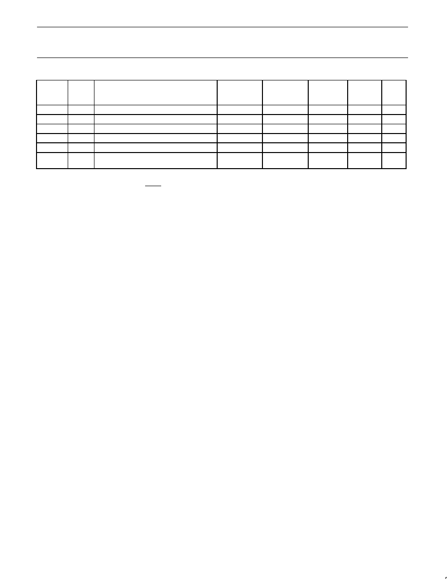
Philips Semiconductors
Product data
P83C654X2/P87C654X2
80C51 8-bit microcontroller family
16 kB OTP/ROM,
256B RAM, low voltage (2.7 to 5.5 V), low power, high speed
(30/33 MHz)
2004 Apr 20
73
t
HD;DAT
Data hold time:
≠ for CBUS compatible masters
≠ for I
2
C≠bus devices
5.0
0
≠
≠
≠
0
≠
0.9
µ
s
t
SU;DAT
Data set-up time
250
≠
100
≠
ns
t
FD
, t
FC
Rise time of both SDA and SCL signals
≠
1000
20 + 0.1 c
b
300
ns
t
FD
, t
FC
Fall time of both SDA and SCL signals
≠
300
20 + 0.1 c
b
300
ns
t
SU; STO
Set-up time for STOP condition
4.0
≠
0.6
≠
µ
s
C
b
Capacitive load for each bus line
≠
400
≠
400
pF
t
SP
Pulse width of spikes which must be sup-
pressed by the input filter
≠
≠
0
50
ns
NOTES:
1. Parameters are valid over operating temperature range unless otherwise specified.
2. Load capacitance for port 0, ALE, and PSEN=100 pF, load capacitance for all outputs = 80 pF
3. Interfacing the microcontroller to devices with float time up to 45ns is permitted. This limited bus contention will not cause damage to port 0
drivers.
4. Parts are guaranteed by design to operate down to 0 Hz.
5. Data shown in the table are the best mathematical models for the set of measured values obtained in tests. If a particular parameter
calculated at a customer specified frequency has a negative value, it should be considered equal to zero.
6. Below 16 MHz this parameter is 4t
CLCL
≠ 133
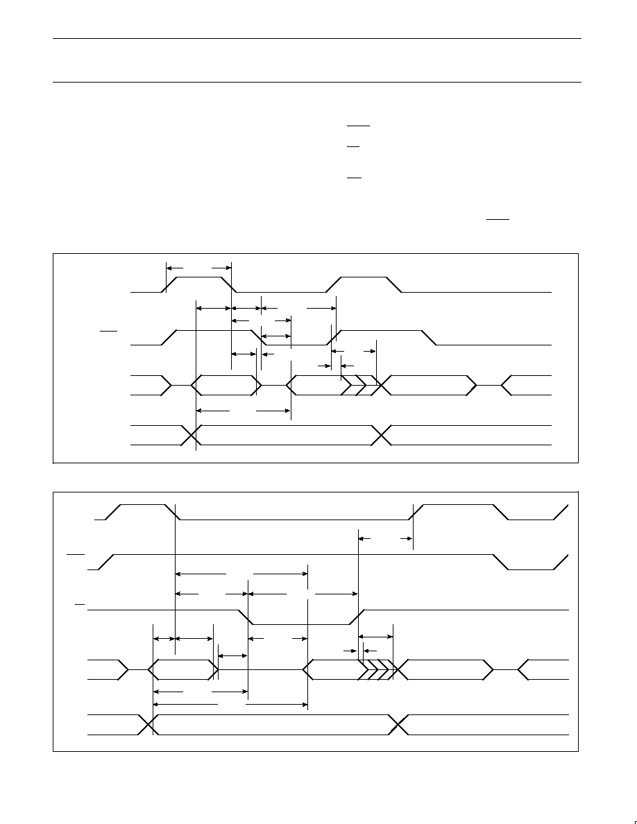
Philips Semiconductors
Product data
P83C654X2/P87C654X2
80C51 8-bit microcontroller family
16 kB OTP/ROM,
256B RAM, low voltage (2.7 to 5.5 V), low power, high speed
(30/33 MHz)
2004 Apr 20
74
EXPLANATION OF THE AC SYMBOLS
Each timing symbol has five characters. The first character is always
`t' (= time). The other characters, depending on their positions,
indicate the name of a signal or the logical status of that signal. The
designations are:
A ≠ Address
C ≠ Clock
D ≠ Input data
H ≠ Logic level HIGH
I ≠ Instruction (program memory contents)
L ≠ Logic level LOW, or ALE
P ≠ PSEN
Q ≠ Output data
R ≠ RD signal
t ≠ Time
V ≠ Valid
W ≠ WR signal
X ≠ No longer a valid logic level
Z ≠ Float
Examples: t
AVLL
= Time for address valid to ALE LOW.
t
LLPL
=Time for ALE LOW to PSEN LOW.
t
PXIZ
ALE
PSEN
PORT 0
PORT 2
A0≠A15
A8≠A15
A0≠A7
A0≠A7
t
AVLL
t
PXIX
t
LLAX
INSTR IN
t
LHLL
t
PLPH
t
LLIV
t
PLAZ
t
LLPL
t
AVIV
SU00006
t
PLIV
Figure 41. External Program Memory Read Cycle
ALE
PSEN
PORT 0
PORT 2
RD
A0≠A7
FROM RI OR DPL
DATA IN
A0≠A7 FROM PCL
INSTR IN
P2.0≠P2.7 OR A8≠A15 FROM DPF
A0≠A15 FROM PCH
t
WHLH
t
LLDV
t
LLWL
t
RLRH
t
LLAX
t
RLAZ
t
AVLL
t
RHDX
t
RHDZ
t
AVWL
t
AVDV
t
RLDV
SU00025
Figure 42. External Data Memory Read Cycle
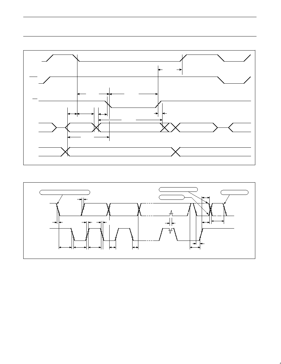
Philips Semiconductors
Product data
P83C654X2/P87C654X2
80C51 8-bit microcontroller family
16 kB OTP/ROM,
256B RAM, low voltage (2.7 to 5.5 V), low power, high speed
(30/33 MHz)
2004 Apr 20
75
t
LLAX
ALE
PSEN
PORT 0
PORT 2
WR
A0≠A7
FROM RI OR DPL
DATA OUT
A0≠A7 FROM PCL
INSTR IN
P2.0≠P2.7 OR A8≠A15 FROM DPF
A0≠A15 FROM PCH
t
WHLH
t
LLWL
t
WLWH
t
AVLL
t
AVWL
t
QVWX
t
WHQX
t
QVWH
SU00026
Figure 43. External Data Memory Write Cycle
SU01742
0.3 VDD
SDA
(INPUT/OUTPUT)
SCL
(INPUT/OUTPUT)
0.7 VDD
t
SP
START or repeated START condition
repeated START condition
STOP condition
START condition
0.7 V
DD
0.3 V
DD
t
SU;DAT3
t
SU;DAT2
t
SU; STO
t
HD;STA
t
LOW
t
HIGH
t
SU;DAT1
t
HD;DAT
t
BUF
t
SU;STA
t
RD
t
RC
t
FC
t
FD
Figure 44. Timing I
2
C interface

Philips Semiconductors
Product data
P83C654X2/P87C654X2
80C51 8-bit microcontroller family
16 kB OTP/ROM,
256B RAM, low voltage (2.7 to 5.5 V), low power, high speed
(30/33 MHz)
2004 Apr 20
76
0
1
2
3
4
5
6
7
8
INSTRUCTION
ALE
CLOCK
OUTPUT DATA
WRITE TO SBUF
INPUT DATA
CLEAR RI
SET TI
SET RI
t
XLXL
t
QVXH
t
XHQX
t
XHDX
t
XHDV
SU00027
1
2
3
0
4
5
6
7
VALID
VALID
VALID
VALID
VALID
VALID
VALID
VALID
Figure 45. Shift Register Mode Timing
VCC≠0.5
0.45V
0.7VCC
0.2VCC≠0.1
t
CHCL
t
CLCL
t
CLCH
t
CLCX
t
CHCX
SU00009
Figure 46. External Clock Drive
VCC≠0.5
0.45V
0.2VCC+0.9
0.2VCC≠0.1
NOTE:
AC inputs during testing are driven at V
CC
≠0.5 for a logic `1' and 0.45V for a logic `0'.
Timing measurements are made at V
IH
min for a logic `1' and V
IL
max for a logic `0'.
SU00717
Figure 47. AC Testing Input/Output
VLOAD
VLOAD+0.1V
VLOAD≠0.1V
VOH≠0.1V
VOL+0.1V
NOTE:
TIMING
REFERENCE
POINTS
For timing purposes, a port is no longer floating when a 100mV change from
load voltage occurs, and begins to float when a 100mV change from the loaded
V
OH
/V
OL
level occurs. I
OH
/I
OL
±
20mA.
SU00718
Figure 48. Float Waveform
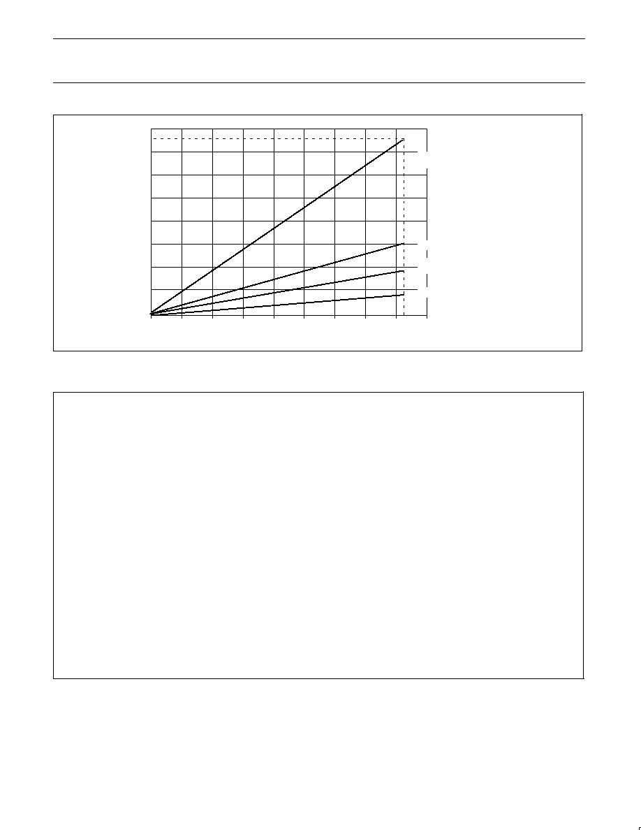
Philips Semiconductors
Product data
P83C654X2/P87C654X2
80C51 8-bit microcontroller family
16 kB OTP/ROM,
256B RAM, low voltage (2.7 to 5.5 V), low power, high speed
(30/33 MHz)
2004 Apr 20
77
SU01684
TYP ACTIVE MODE
MAX IDLE MODE
I
CC
MAX = 0.22
FREQ. + 1.0
TYP IDLE MODE
5
4
8
12
16
FREQ AT XTAL1 (MHz)
20
24
28
32
36
15
25
I CC
(mA)
10
20
MAX ACTIVE MODE
I
CC
MAX = 1.1
FREQ. + 1.0
35
30
40
Figure 49. I
CC
vs. FREQ for 12-clock operation
Valid only within frequency specifications of the specified operating voltage
/*
## as31 version V2.10
/ *js* /
##
##
## source file: idd_ljmp1.asm
## list file: idd_ljmp1.lst created Fri Apr 20 15:51:40 2001
##
##########################################################
#0000 # AUXR equ 08Eh
#0000 # CKCON equ 08Fh
#
#
#0000 # org 0
#
# LJMP_LABEL:
0000 /75;/8E;/01; # MOV AUXR,#001h ; turn off ALE
0003 /02;/FF;/FD; # LJMP LJMP_LABEL ; jump to end of address space
0005 /00; # NOP
#
#FFFD # org 0fffdh
#
# LJMP_LABEL:
#
FFFD /02;/FD;FF; # LJMP LJMP_LABEL
# ; NOP
#
#
*/"
SU01499
Figure 50. Source code used in measuring I
DD
operational

Philips Semiconductors
Product data
P83C654X2/P87C654X2
80C51 8-bit microcontroller family
16 kB OTP/ROM,
256B RAM, low voltage (2.7 to 5.5 V), low power, high speed
(30/33 MHz)
2004 Apr 20
78
V
CC
P0
EA
RST
XTAL1
XTAL2
V
SS
V
CC
V
CC
V
CC
I
CC
(NC)
CLOCK SIGNAL
SU00719
Figure 51. I
CC
Test Condition, Active Mode
All other pins are disconnected
V
CC
P0
EA
RST
XTAL1
XTAL2
V
SS
V
CC
V
CC
I
CC
(NC)
CLOCK SIGNAL
SU00720
Figure 52. I
CC
Test Condition, Idle Mode
All other pins are disconnected
VCC≠0.5
0.45V
0.7VCC
0.2VCC≠0.1
t
CHCL
t
CLCL
t
CLCH
t
CLCX
t
CHCX
SU00009
Figure 53. Clock Signal Waveform for I
CC
Tests in Active and Idle Modes
t
CLCH
= t
CHCL
= 5ns
V
CC
P0
EA
RST
XTAL1
XTAL2
VSS
V
CC
V
CC
I
CC
(NC)
SU00016
Figure 54. I
CC
Test Condition, Power-down mode
All other pins are disconnected. V
CC
= 2 V to 5.5 V

Philips Semiconductors
Product data
P83C654X2/P87C654X2
80C51 8-bit microcontroller family
16 kB OTP/ROM,
256B RAM, low voltage (2.7 to 5.5 V), low power, high speed
(30/33 MHz)
2004 Apr 20
79
EPROM CHARACTERISTICS
The 87C654X2 can be programmed by using a modified Improved
Quick-Pulse Programming
TM
algorithm. It differs from older methods
in the value used for V
PP
(programming supply voltage) and in the
width and number of the ALE/PROG pulses.
The family contains two signature bytes that can be read and used
by an EPROM programming system to identify the device. The
signature bytes identify the device as being manufactured by
Philips.
Table 15 shows the logic levels for reading the signature byte, and
for programming the program memory, the encryption table, and the
security bits. The circuit configuration and waveforms for quick-pulse
programming are shown in Figures 55 and 56. Figure 57 shows the
circuit configuration for normal program memory verification.
Quick-Pulse Programming
The setup for microcontroller quick-pulse programming is shown in
Figure 55. Note that the device is running with a 4 to 6MHz
oscillator. The reason the oscillator needs to be running is that the
device is executing internal address and program data transfers.
The address of the EPROM location to be programmed is applied to
ports 1 and 2, as shown in Figure 55. The code byte to be
programmed into that location is applied to port 0. RST, PSEN and
pins of ports 2 and 3 specified in Table 15 are held at the `Program
Code Data' levels indicated in Table 15. The ALE/PROG is pulsed
LOW 5 times as shown in Figure 56.
To program the encryption table, repeat the 5 pulse programming
sequence for addresses 0 through 1FH, using the `Pgm Encryption
Table' levels. Do not forget that after the encryption table is
programmed, verification cycles will produce only encrypted data.
To program the security bits, repeat the 5 pulse programming
sequence using the `Pgm Security Bit' levels. After one security bit is
programmed, further programming of the code memory and
encryption table is disabled. However, the other security bits can still
be programmed.
Note that the EA/V
PP
pin must not be allowed to go above the
maximum specified V
PP
level for any amount of time. Even a narrow
glitch above that voltage can cause permanent damage to the
device. The V
PP
source should be well regulated and free of glitches
and overshoot.
Program Verification
If security bits 2 and 3 have not been programmed, the on-chip
program memory can be read out for program verification. The
address of the program memory locations to be read is applied to
ports 1 and 2 as shown in Figure 57. The other pins are held at the
`Verify Code Data' levels indicated in Table 15. The contents of the
address location will be emitted on port 0. External pull-ups are
required on port 0 for this operation.
If the 64 byte encryption table has been programmed, the data
presented at port 0 will be the exclusive NOR of the program byte
with one of the encryption bytes. The user will have to know the
encryption table contents in order to correctly decode the verification
data. The encryption table itself cannot be read out.
Reading the Signature Bytes
The signature bytes are read by the same procedure as a normal
verification of locations 030H and 031H, except that P3.6 and P3.7
need to be pulled to a logic LOW. The values are:
(030H) = 15H indicates manufactured by Philips
(031H) = 99H
(060H) = 02H
Program/Verify Algorithms
Any algorithm in agreement with the conditions listed in Table 15,
and which satisfies the timing specifications, is suitable.
Security Bits
With none of the security bits programmed the code in the program
memory can be verified. If the encryption table is programmed, the
code will be encrypted when verified. When only security bit 1 (see
Table 16) is programmed, MOVC instructions executed from
external program memory are disabled from fetching code bytes
from the internal memory, EA is latched on Reset and all further
programming of the EPROM is disabled. When security bits 1 and 2
are programmed, in addition to the above, verify mode is disabled.
When all three security bits are programmed, all of the conditions
above apply and all external program memory execution is disabled.
Encryption Array
64 bytes of encryption array are initially unprogrammed (all 1s).
TM
Trademark phrase of Intel Corporation.

Philips Semiconductors
Product data
P83C654X2/P87C654X2
80C51 8-bit microcontroller family
16 kB OTP/ROM,
256B RAM, low voltage (2.7 to 5.5 V), low power, high speed
(30/33 MHz)
2004 Apr 20
80
Table 15.
EPROM Programming Modes
MODE
RST
PSEN
ALE/PROG
EA/V
PP
P2.7
P2.6
P3.7
P3.6
P3.3
Read signature
1
0
1
1
0
0
0
0
X
Program code data
1
0
0*
V
PP
1
0
1
1
X
Verify code data
1
0
1
1
0
0
1
1
X
Pgm encryption table
1
0
0*
V
PP
1
0
1
0
X
Pgm security bit 1
1
0
0*
V
PP
1
1
1
1
X
Pgm security bit 2
1
0
0*
V
PP
1
1
0
0
X
Pgm security bit 3
1
0
0*
V
PP
0
1
0
1
X
Program to 6-clock mode
1
0
0*
V
PP
0
0
1
0
0
Verify 6-clock
4
1
0
1
1
e
0
0
1
1
Verify security bits
5
1
0
1
1
e
0
1
0
X
NOTES:
1. `0' = Valid LOW for that pin, `1' = valid HIGH for that pin.
2. V
PP
= 12.75 V
±
0.25 V.
3. V
CC
= 5 V
±
10 % during programming and verification.
4. Bit is output on P0.4 (1 = 12x, 0 = 6x).
5. Security bit one is output on P0.7.
Security bit two is output on P0.6.
Security bit three is output on P0.3.
*
ALE/PROG receives 5 programming pulses for code data (also for user array; 5 pulses for encryption or security bits) while V
PP
is held at
12.75 V. Each programming pulse is LOW for 100
µ
s (
±
10
µ
s) and HIGH for a minimum of 10
µ
s.
Table 16.
Program Security Bits for EPROM Devices
PROGRAM LOCK BITS
1, 2
SB1
SB2
SB3
PROTECTION DESCRIPTION
1
U
U
U
No Program Security features enabled. (Code verify will still be encrypted by the Encryption Array if
programmed.)
2
P
U
U
MOVC instructions executed from external program memory are disabled from fetching code bytes
from internal memory, EA is sampled and latched on Reset, and further programming of the EPROM
is disabled.
3
P
P
U
Same as 2, also verify is disabled.
4
P
P
P
Same as 3, external execution is disabled. Internal data RAM is not accessible.
NOTES:
1. P ≠ programmed. U ≠ unprogrammed.
2. Any other combination of the security bits is not defined.
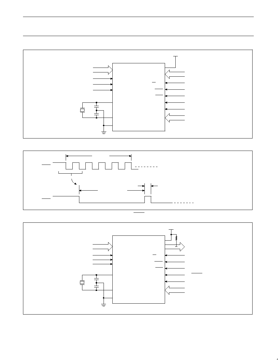
Philips Semiconductors
Product data
P83C654X2/P87C654X2
80C51 8-bit microcontroller family
16 kB OTP/ROM,
256B RAM, low voltage (2.7 to 5.5 V), low power, high speed
(30/33 MHz)
2004 Apr 20
81
A0≠A7
1
1
1
4≠6MHz
+5V
PGM DATA
+12.75V
5 PULSES TO GROUND
0
1
0
A8≠A13
P1
RST
P3.6
P3.7
XTAL2
XTAL1
VSS
VCC
P0
EA/VPP
ALE/PROG
PSEN
P2.7
P2.6
P2.0≠P2.5
OTP
SU01746
A8≠A15 are programming addresses
(not external memory addresses per
device pin out)
Figure 55. Programming Configuration
ALE/PROG:
ALE/PROG:
1
0
1
0
5 PULSES
t
GLGH
= 100
µ
s
±
10
µ
s
t
GHGL
= 10
µ
s MIN
SU00875
1
2
3
4
5
SEE EXPLODED VIEW BELOW
1
Figure 56. PROG Waveform
A0≠A7
1
1
1
+5V
PGM DATA
1
1
0
0 ENABLE
0
A8≠A13
P1
RST
P3.6
P3.7
XTAL2
XTAL1
VSS
VCC
P0
EA/VPP
ALE/PROG
PSEN
P2.7
P2.6
P2.0≠P2.5
OTP
SU01747
4≠6MHz
A8≠A15 are programming addresses
(not external memory addresses per
device pin out)
Figure 57. Program Verification
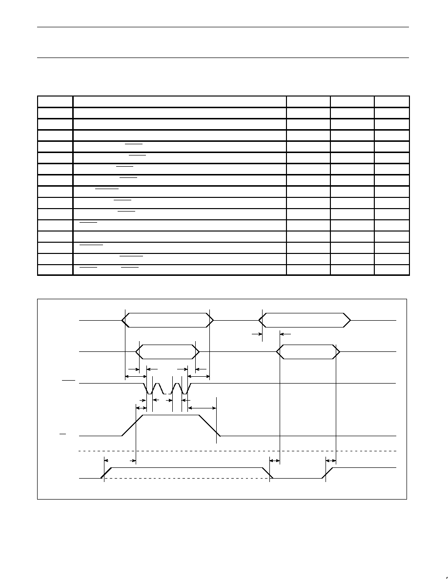
Philips Semiconductors
Product data
P83C654X2/P87C654X2
80C51 8-bit microcontroller family
16 kB OTP/ROM,
256B RAM, low voltage (2.7 to 5.5 V), low power, high speed
(30/33 MHz)
2004 Apr 20
82
EPROM PROGRAMMING AND VERIFICATION CHARACTERISTICS
T
amb
= 21
∞
C to +27
∞
C, V
CC
= 5 V
±
10 %, V
SS
= 0 V (See Figure 58)
SYMBOL
PARAMETER
MIN
MAX
UNIT
V
PP
Programming supply voltage
12.5
13.0
V
I
PP
Programming supply current
50
1
mA
1/t
CLCL
Oscillator frequency
4
6
MHz
t
AVGL
Address setup to PROG LOW
48t
CLCL
t
GHAX
Address hold after PROG
48t
CLCL
t
DVGL
Data setup to PROG LOW
48t
CLCL
t
GHDX
Data hold after PROG
48t
CLCL
t
EHSH
P2.7 (ENABLE) HIGH to V
PP
48t
CLCL
t
SHGL
V
PP
setup to PROG LOW
10
µ
s
t
GHSL
V
PP
hold after PROG
10
µ
s
t
GLGH
PROG width
90
110
µ
s
t
AVQV
Address to data valid
48t
CLCL
t
ELQZ
ENABLE LOW to data valid
48t
CLCL
t
EHQZ
Data float after ENABLE
0
48t
CLCL
t
GHGL
PROG HIGH to PROG LOW
10
µ
s
NOTE:
1. Not tested.
PROGRAMMING
*
VERIFICATION
*
ADDRESS
ADDRESS
DATA IN
DATA OUT
LOGIC 1
LOGIC 1
LOGIC 0
t
AVQV
t
EHQZ
t
ELQV
t
SHGL
t
GHSL
t
GLGH
t
GHGL
t
AVGL
t
GHAX
t
DVGL
t
GHDX
P1.0≠P1.7
P2.0≠P2.5
P3.4
(A0 ≠ A14)
PORT 0
P0.0 ≠ P0.7
(D0 ≠ D7)
ALE/PROG
EA/V
PP
P2.7
**
SU00871
t
EHSH
NOTES:
*
FOR PROGRAMMING CONFIGURATION SEE FIGURE 55.
FOR VERIFICATION CONDITIONS SEE FIGURE 57.
**
SEE TABLE 15.
Figure 58. EPROM Programming and Verification
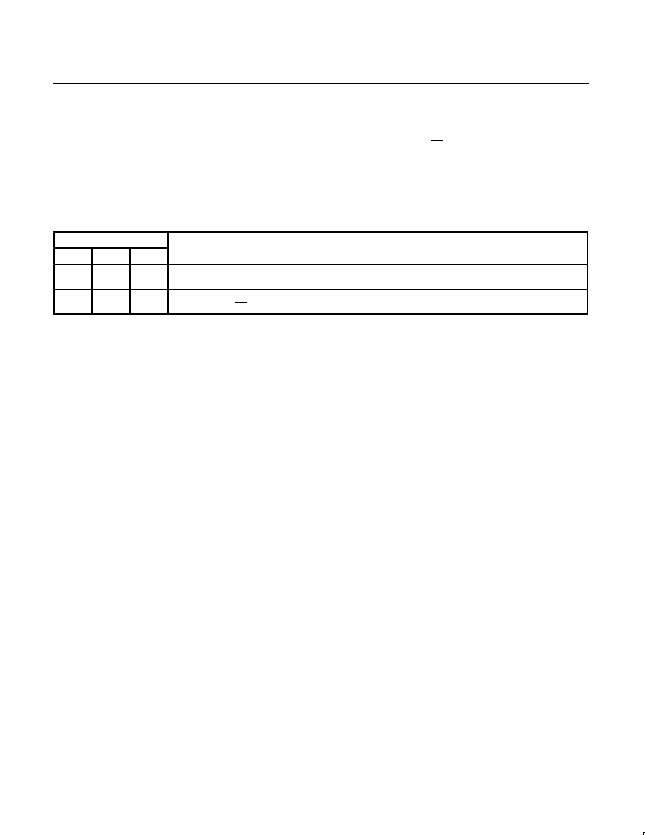
Philips Semiconductors
Product data
P83C654X2/P87C654X2
80C51 8-bit microcontroller family
16 kB OTP/ROM,
256B RAM, low voltage (2.7 to 5.5 V), low power, high speed
(30/33 MHz)
2004 Apr 20
83
MASK ROM DEVICES
Security Bits
With none of the security bits programmed the code in the program
memory can be verified. If the encryption table is programmed, the
code will be encrypted when verified. When only security bit 1 (see
Table 17) is programmed, MOVC instructions executed from
external program memory are disabled from fetching code bytes
from the internal memory, EA is latched on Reset and all further
programming of the EPROM is disabled. When security bits 1 and 2
are programmed, in addition to the above, verify mode is disabled.
Encryption Array
64 bytes of encryption array are initially unprogrammed (all 1s).
Table 17.
Program Security Bits
PROGRAM LOCK BITS
1, 2
SB1
SB2
PROTECTION DESCRIPTION
1
U
U
No Program Security features enabled.
(Code verify will still be encrypted by the Encryption Array if programmed.)
2
P
U
MOVC instructions executed from external program memory are disabled from fetching code bytes from
internal memory, EA is sampled and latched on Reset, and further programming of the EPROM is disabled.
NOTES:
1. P ≠ programmed. U ≠ unprogrammed.
2. Any other combination of the security bits is not defined.
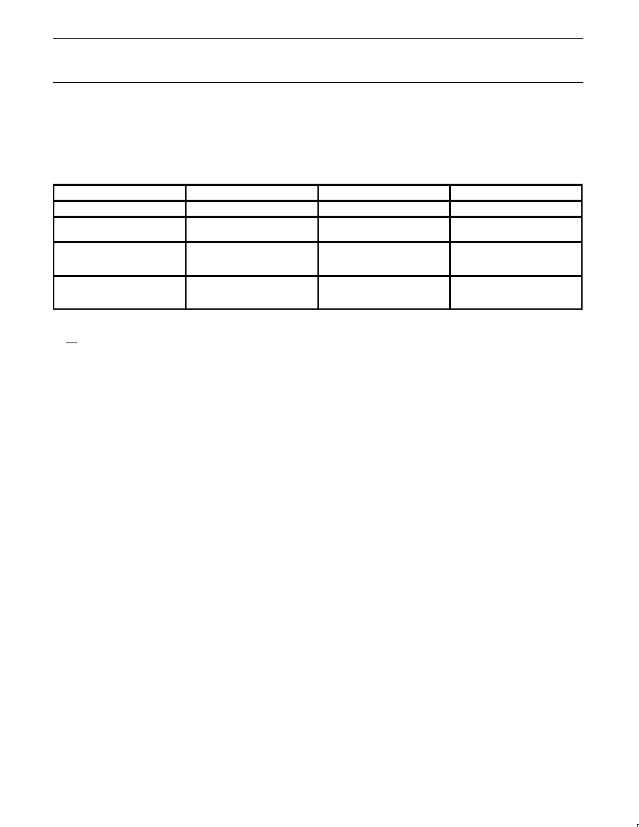
Philips Semiconductors
Product data
P83C654X2/P87C654X2
80C51 8-bit microcontroller family
16 kB OTP/ROM,
256B RAM, low voltage (2.7 to 5.5 V), low power, high speed
(30/33 MHz)
2004 Apr 20
84
ROM CODE SUBMISSION FOR 16K ROM DEVICES
When submitting ROM code for the 16K ROM devices, the following must be specified:
1. 16 kbyte user ROM data
2. 64 byte ROM encryption key
3. ROM security bits.
ADDRESS
CONTENT
BIT(S)
COMMENT
0000H to 3FFFH
DATA
7:0
User ROM Data
4000H to 403FH
KEY
7:0
ROM Encryption Key
FFH = no encryption
4040H
SEC
0
ROM Security Bit 1
0 = enable security
1 = disable security
4040H
SEC
1
ROM Security Bit 2
0 = enable security
1 = disable security
Security Bit 1: When programmed, this bit has two effects on masked ROM parts:
1. External MOVC is disabled, and
2. EA is latched on Reset.
Security Bit 2: When programmed, this bit inhibits Verify User ROM.
NOTE: Security Bit 2 cannot be enabled unless Security Bit 1 is enabled.
If the ROM Code file does not include the options, the following information must be included with the ROM code.
For each of the following, check the appropriate box, and send to Philips along with the code:
Security Bit #1:
V
Enabled
V
Disabled
Security Bit #2:
V
Enabled
V
Disabled
Encryption:
V
No
V
Yes
If Yes, must send key file.
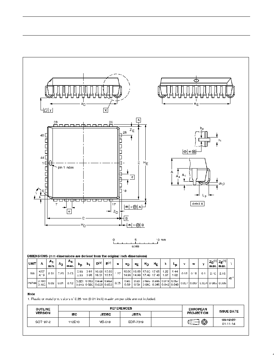
Philips Semiconductors
Product data
P83C654X2/P87C654X2
80C51 8-bit microcontroller family
16 kB OTP/ROM,
256B RAM, low voltage (2.7 to 5.5 V), low power, high speed
(30/33 MHz)
2004 Apr 20
85
PLCC44:
plastic leaded chip carrier; 44 leads
SOT187-2
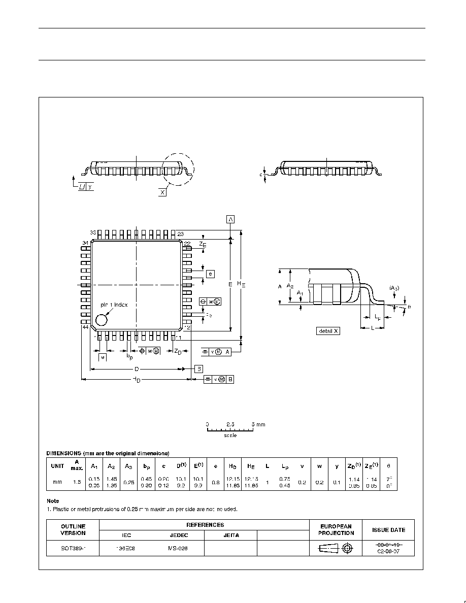
Philips Semiconductors
Product data
P83C654X2/P87C654X2
80C51 8-bit microcontroller family
16 kB OTP/ROM,
256B RAM, low voltage (2.7 to 5.5 V), low power, high speed
(30/33 MHz)
2004 Apr 20
86
LQFP44:
plastic low profile quad flat package; 44 leads; body 10 x 10 x 1.4 mm
SOT389-1
Philips Semiconductors
Product data
P83C654X2/P87C654X2
80C51 8-bit microcontroller family
16 kB OTP/ROM,
256B RAM, low voltage (2.7 to 5.5 V), low power, high speed
(30/33 MHz)
2004 Apr 20
87
REVISION HISTORY
Rev
Date
Description
_2
20040420
Product data (9397 750 13173)
Modifications:
∑
Update Special Function Registers table.
∑
Remove P3.4 from Figures 55 and 57.
_1
20030213
Product data (9397 750 10814)
Philips Semiconductors
Product data
P83C654X2/P87C654X2
80C51 8-bit microcontroller family
16 kB OTP/ROM,
256B RAM, low voltage (2.7 to 5.5 V), low power, high speed
(30/33 MHz)
2004 Apr 20
88
Purchase of Philips I
2
C components conveys a license under the Philips' I
2
C patent
to use the components in the I
2
C system provided the system conforms to the
I
2
C specifications defined by Philips. This specification can be ordered using the
code 9398 393 40011.
Definitions
Short-form specification -- The data in a short-form specification is extracted from a full data sheet with the same type number and title. For detailed information see
the relevant data sheet or data handbook.
Limiting values definition -- Limiting values given are in accordance with the Absolute Maximum Rating System (IEC 60134). Stress above one or more of the limiting
values may cause permanent damage to the device. These are stress ratings only and operation of the device at these or at any other conditions above those given
in the Characteristics sections of the specification is not implied. Exposure to limiting values for extended periods may affect device reliability.
Application information -- Applications that are described herein for any of these products are for illustrative purposes only. Philips Semiconductors make no
representation or warranty that such applications will be suitable for the specified use without further testing or modification.
Disclaimers
Life support -- These products are not designed for use in life support appliances, devices, or systems where malfunction of these products can reasonably be
expected to result in personal injury. Philips Semiconductors customers using or selling these products for use in such applications do so at their own risk and agree
to fully indemnify Philips Semiconductors for any damages resulting from such application.
Right to make changes -- Philips Semiconductors reserves the right to make changes in the products--including circuits, standard cells, and/or software--described
or contained herein in order to improve design and/or performance. When the product is in full production (status `Production'), relevant changes will be communicated
via a Customer Product/Process Change Notification (CPCN). Philips Semiconductors assumes no responsibility or liability for the use of any of these products, conveys
no license or title under any patent, copyright, or mask work right to these products, and makes no representations or warranties that these products are free from patent,
copyright, or mask work right infringement, unless otherwise specified.
Contact information
For additional information please visit
http://www.semiconductors.philips.com.
Fax: +31 40 27 24825
For sales offices addresses send e-mail to:
sales.addresses@www.semiconductors.philips.com.
©
Koninklijke Philips Electronics N.V. 2004
All rights reserved. Printed in U.S.A.
Date of release: 04-04
Document order number:
9397 750 13173
Philips
Semiconductors
Data sheet status
[1]
Objective data
Preliminary data
Product data
Product
status
[2] [3]
Development
Qualification
Production
Definitions
This data sheet contains data from the objective specification for product development.
Philips Semiconductors reserves the right to change the specification in any manner without notice.
This data sheet contains data from the preliminary specification. Supplementary data will be published
at a later date. Philips Semiconductors reserves the right to change the specification without notice, in
order to improve the design and supply the best possible product.
This data sheet contains data from the product specification. Philips Semiconductors reserves the
right to make changes at any time in order to improve the design, manufacturing and supply. Relevant
changes will be communicated via a Customer Product/Process Change Notification (CPCN).
Data sheet status
[1] Please consult the most recently issued data sheet before initiating or completing a design.
[2] The product status of the device(s) described in this data sheet may have changed since this data sheet was published. The latest information is available on the Internet at URL
http://www.semiconductors.philips.com.
[3] For data sheets describing multiple type numbers, the highest-level product status determines the data sheet status.
Level
I
II
III