 | –≠–ª–µ–∫—Ç—Ä–æ–Ω–Ω—ã–π –∫–æ–º–ø–æ–Ω–µ–Ω—Ç: P83CL882 | –°–∫–∞—á–∞—Ç—å:  PDF PDF  ZIP ZIP |
Document Outline
- CONTENTS
- FEATURES
- GENERAL DESCRIPTION
- ORDERING INFORMATION
- PINNING INFORMATION
- FUNCTIONAL DESCRIPTION
- INSTRUCTION SET
- APPLICATION INFORMATION
- HOW TO ESTIMATE P83CL882 POWER CONSUMPTION
- LIMITING VALUES
- CHARACTERISTICS
- PACKAGE OUTLINE
- SOLDERING
- DATA SHEET STATUS
- DEFINITIONS
- DISCLAIMERS
DATA SHEET
Product specification
File under Integrated Circuits, IC22
2001 Jun 19
INTEGRATED CIRCUITS
P83CL882
80C51 Ultra Low Power (ULP)
telephony controller

2001 Jun 19
2
Philips Semiconductors
Product specification
80C51 Ultra Low Power (ULP) telephony controller
P83CL882
CONTENTS
1
FEATURES
2
GENERAL DESCRIPTION
3
ORDERING INFORMATION
4
BLOCK DIAGRAM
5
PINNING INFORMATION
5.1
Pin configuration
5.2
Pin description
6
FUNCTIONAL DESCRIPTION
6.1
Oscillator circuitry
6.2
The CPU
6.3
Interrupt controller
6.4
Port control logic
6.5
Timer 0 and Timer 1 event counters
6.6
Timer 2
6.7
Watchdog Timer
6.8
I
2
C-bus serial I/O (master/slave interface)
6.9
MSK modem
6.10
Internal Data Memory
6.11
Special Function Registers overview
7
INSTRUCTION SET
7.1
Instruction map
8
APPLICATION INFORMATION
8.1
Introduction
8.2
Differences between P83CL882 and the
Metalink EH emulation system
8.3
The asynchronous handshake CPU
9
HOW TO ESTIMATE P83CL882 POWER
CONSUMPTION
9.1
General
9.2
Modes
9.3
Examples of power consumption estimation
10
LIMITING VALUES
11
CHARACTERISTICS
12
PACKAGE OUTLINE
13
SOLDERING
13.1
Introduction to soldering surface mount
packages
13.2
Reflow soldering
13.3
Wave soldering
13.4
Manual soldering
13.5
Suitability of surface mount IC packages for
wave and reflow soldering methods
14
DATA SHEET STATUS
15
DEFINITIONS
16
DISCLAIMERS
17
PURCHASE OF PHILIPS I
2
C COMPONENTS

2001 Jun 19
3
Philips Semiconductors
Product specification
80C51 Ultra Low Power (ULP) telephony controller
P83CL882
1
FEATURES
∑
Full static asynchronous handshake 80C51 CPU;
enhanced 8-bit architecture with:
≠ Standard 80C51 instruction set
≠ CPU speed independent of clock frequency, average
speed: 4.8 Mips at 3.0 V
≠ Non-page oriented instructions
≠ Direct addressing
≠ Four 8-byte RAM register banks
≠ Stack depth limited only by available internal RAM
(maximum 128 bytes)
≠ Multiply, divide, subtract and compare instructions.
∑
17 source, 17 vector interrupt structure with two priority
levels, polarity and sensitivity choice
∑
24 general purpose I/O pins
∑
Timer 0 and 1: two standard 16-bit timer/event counters
∑
Timer 2: 16-bit timer/event counter with capture,
compare and auto-reload function
∑
Watchdog Timer
∑
Wake-up counter
∑
Idle and Power-down modes
∑
4-kbyte ROM: mask programmed read only memory
∑
Supply voltage: 1.8 to 3.6 V
∑
128 bytes RAM
∑
Internal crystal oscillator
∑
Reset I/O pin for external reset from master or to slave
∑
MSK modem including Manchester encoder/decoder
with 2 digital outputs (by SW) for analog cordless
telephones (standards CT0/CT1/CT1+)
∑
I
2
C-bus master/slave (transmitter/receiver, maximum
frequency 400 kHz).
2
GENERAL DESCRIPTION
The P83CL882 is manufactured in an advanced CMOS
technology. The P83CL882 is a member of the VTELX
family of low-power, low-voltage 80CL51 microcontrollers
with advanced features for telecom applications. The
Philips exclusive, asynchronous handshaking technology
has been used for the CPU implementation which makes
the CPU to run at its maximum speed independent of the
used crystal frequency.
The P83CL882 is especially suited for low cost analog
cordless telephone applications (CT0, CT1 and CT1+
standards) and wired feature phones. For this purpose,
functions like MSK modem and I
2
C-bus are integrated
on-chip.
The device is optimized for low-power consumption. It has
two software selectable modes for power reduction: Idle
and Power-down. In addition, the clock to all unused
peripheral blocks can be switched off.
The instruction set is based on that of the 80C51. The
P83CL882 also functions as an arithmetic processor
having facilities for both binary and BCD arithmetic plus
bit-handling capabilities. The instruction set consists of
over 100 instructions: 49 one-byte, 46 two-byte, and
16 three-byte. Port 2 is not incorporated, therefore there is
no external data or memory access and the MOVX
operations cannot be used.
3
ORDERING INFORMATION
TYPE NUMBER
PACKAGE
NAME
DESCRIPTION
VERSION
P83CL882T/xxx
TSSOP32
plastic thin shrink small outline package; 32 leads;
body width 6.1 mm
SOT487-1
2001
Jun
19
4
Philips Semiconductors
Product specification
80C51 Ultr
a Lo
w P
o
w
e
r
(ULP) telephon
y controller
P83CL882
This text is here in white to force landscape pages to be rotated correctly when browsing through the pdf in the Acrobat reader.This text is here in
_
white to force landscape pages to be rotated correctly when browsing through the pdf in the Acrobat reader.This text is here inThis text is here in
white to force landscape pages to be rotated correctly when browsing through the pdf in the Acrobat reader. white to force landscape pages to be ...
4
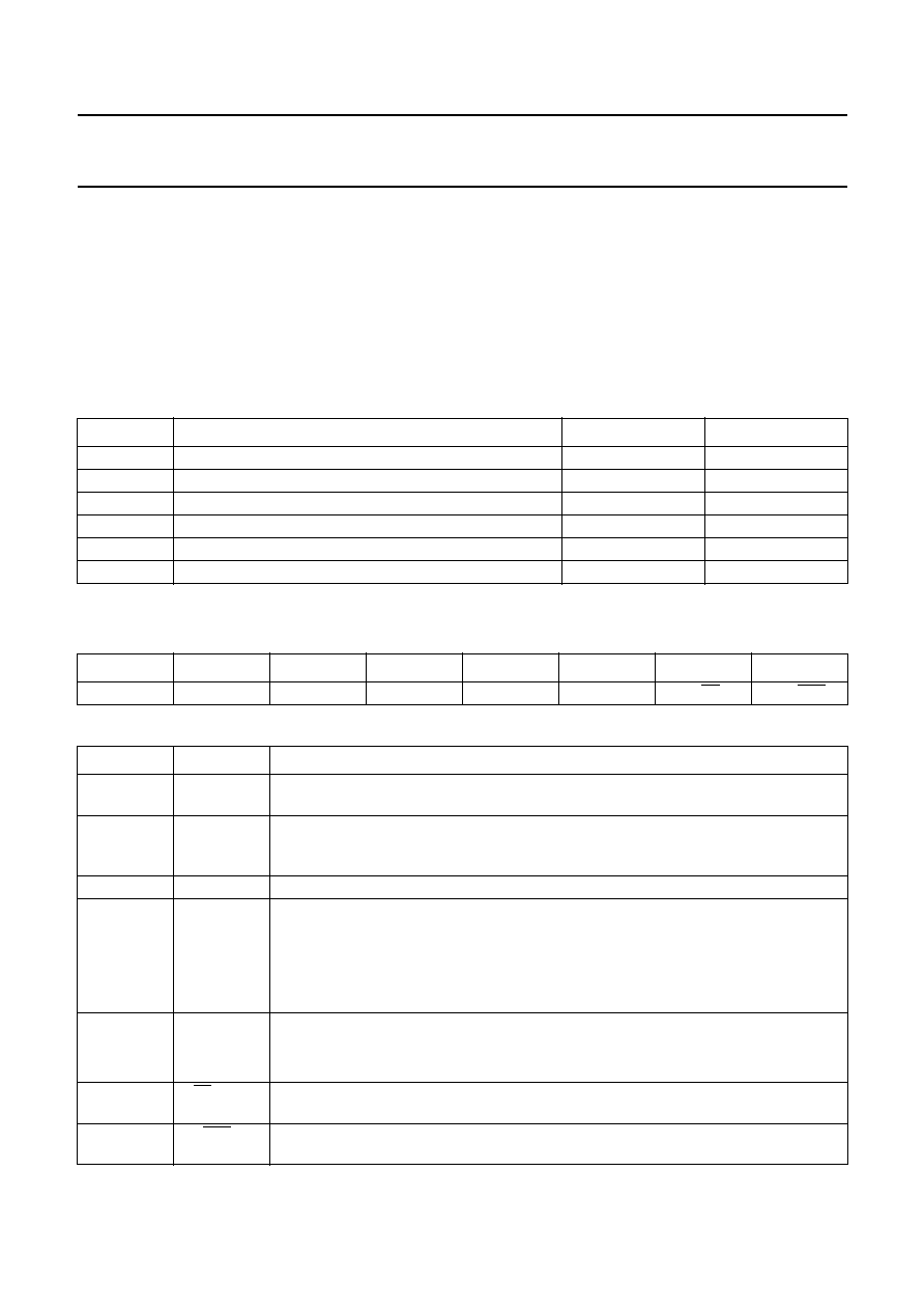
BLOCK DIA
GRAM
handbook, full pagewidth
MGU258
(2)
T0
(2)
T1
TIMER 0
TIMER 1
ROM
INTERRUPT
CONTROL
RAM
internal bus
CPU
80C51
RST
IRST
mode
selection
SELECT
XTM
MODE AND
TEST CONTROL
(2)
MOUT2
to
MOUT0
fper
fosc
fosc
MSK MODEM
XTAL2
XTAL1
AMPLITUDE
CONTROLLED
OSCILLATOR
OSCILLATOR
COMPARATOR
BLOCK
PSC2
PSC1
MIN
VDD
VSS VDDP VSSP
PORT
CONTROL
PORT 0
PORT 3
TIMER 2
I
2
C-BUS
INTERFACE
WATCHDOG
TIMER
PORT 1
fpsc
fper
fper
fpsc
fpsc
SDA
(1)
SCL
(1)
T2OUT
(1)
T2EX
(1)
T2
(1)
P3
P1
P0
P83CL882
Fig.1 Simplified block diagram.
(1) Alternative function of Port 1.
(2) Alternative function of Port 3.
2001 Jun 19
5
Philips Semiconductors
Product specification
80C51 Ultra Low Power (ULP) telephony controller
P83CL882
5
PINNING INFORMATION
5.1
Pin configuration
handbook, halfpage
P83CL882
MGU265
1
2
3
4
5
6
7
8
9
10
11
12
13
14
15
16
P3.3
P3.4/T0
P3.5/T1
P3.6
P3.7
P1.2/INT4/T2
P1.1/INT3/T2EX
P1.0/INT2
VSS
VDD
XTAL2
XTAL1
RST
P3.0/MOUT0
P3.1/INT1/MOUT1
P3.2/INT0/MOUT2
VSSP
VDDP
P1.5/INT7
P1.4/INT6/CLKOUT
P1.3/INT5
P0.7
P0.6
P0.5
P0.4
P0.3
P0.2
P0.1
P0.0
P1.7/INT9/SDA
P1.6/INT8/SCL
MIN
32
31
30
29
28
27
26
25
24
23
22
21
20
19
18
17
Fig.2 Pin configuration (TSSOP32/SOT487-1).

2001 Jun 19
6
Philips Semiconductors
Product specification
80C51 Ultra Low Power (ULP) telephony controller
P83CL882
5.2
Pin description
Table 1
Pin description for TSSOP32 (SOT487-1)
Note
1. For high current drive capability on I/Os all supply pins should be connected.
SYMBOL
PIN
TYPE
DESCRIPTION
P3.3
1
I/O
Port 3: P3.3 to P3.7; bidirectional I/O port with two alternative functions.
P3.4 also serves as the Timer 0 external count input (T0). P3.5 also
serves as the Timer 1 external count input (T1).
P3.4/T0
2
I/O
P3.5/T1
3
I/O
P3.6
4
I/O
P3.7
5
I/O
P1.2/INT4/T2
6
I/O
Port 1: P1.2 to P1.0; bidirectional I/O port with alternative functions.
INT4, INT3 and INT2 are the external interrupts 4, 3 and 2 respectively.
P1.2 also serves as Timer 2 input (T2). P1.1 also serves as Timer 2
external input (T2EX).
P1.1/INT3/T2EX
7
I/O
P1.0/INT2
8
I/O
V
SS
(1)
9
S
ground
V
DD
(1)
10
S
power supply voltage
XTAL2
11
O
crystal output
XTAL1
12
I
crystal input; external clock input
RST
13
I/O
reset input/output pin; active LOW
P3.0/MOUT0
14
I/O
Port 3: P3.0 to P3.2; bidirectional I/O port with alternative functions.
MOUT2 to MOUT0 are the MSK outputs (mapped on the lower 3 bits of
Port 3). P3.2 also serves as the external interrupt 0 input (INT1)
and P3.1 as the external interrupt 1 input (INT0).
P3.1/MOUT1/INT1
15
I/O
P3.2/MOUT2/INT0
16
I/O
MIN
17
I
MSK input
P1.6/INT8/SCL
18
I/O
Port 1: P1.6 and P1.7; can only be used as open-drain output or
high-impedance input. Alternative functions: INT8 and INT9, external
interrupt 8 and 9. SCL and SDA I
2
C-bus interface clock and data.
P1.7/INT9/SDA
19
I/O
P0.0 to P0.7
20 to 27
I/O
Port 0: 8-bit bidirectional I/O port. Every port pin can be used as
open-drain, standard port, high-impedance input or push-pull output.
P1.3/INT5
28
I/O
Port 1: P1.3 to P1.5; bidirectional I/O port with alternative functions
INT5, INT6 and INT7: external interrupt 5 to 7. P1.4 also serves as
auxiliary clock output (CLKOUT). P1.5 also serves as the Timer 2 output
(T2OUT).
P1.4/INT6/CLKOUT
29
I/O
P1.5/INT7/T2OUT
30
I/O
V
DDP
(1)
31
S
periphery (I/O) positive supply voltage
V
SSP
(1)
32
S
periphery (I/O) ground
2001 Jun 19
7
Philips Semiconductors
Product specification
80C51 Ultra Low Power (ULP) telephony controller
P83CL882
6
FUNCTIONAL DESCRIPTION
6.1
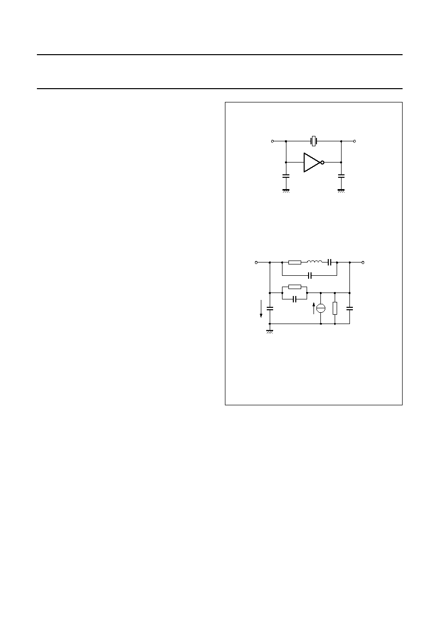
Oscillator circuitry
The on-chip Amplitude Controlled Oscillator (ACO)
circuitry is a single-stage inverting amplifier biased by an
internal feedback resistor R
fb
. The oscillator circuit is
shown in Fig.3.
Two comparators with different characteristics can be
used with the on-chip crystal oscillator. The first one is an
analog comparator built around a differential amplifier and
is intended to be selected when an external ceramic or
crystal resonator is connected to the chip.
The other comparator has a Schmitt trigger input with
a bigger hysteresis which is especially useful when the
P83CL882 is driven from an external clock source.
Two bits in the SYSCON SFR: SELECT and XTM, are
used to configure the oscillator. The SELECT bit
(SYSCON.1) enables the analog comparator or the
hysteresis comparator.
With XTM (SYSCON.0) = 1 (or in Power-down mode;
PCON.1 = 1) the oscillator is switched off and the current
consumption of the oscillator is reduced to zero.
Table 2
Comparator select bits in SYSCON SFR
6.1.1
C
LOCK OSCILLATOR CONNECTIONS
No external components are needed when a quartz crystal
is used to drive the oscillator. When an external ceramic
resonator is used to drive the oscillator, external
components may be required depending upon the ceramic
resonator type; refer to the product specification. Two
different resonator configurations are shown in
Figs 4a and 4b.
To drive the device with an external clock source, apply the
external clock signal to XTAL1, and leave XTAL2 floating,
as shown in Fig.4c. If the amplitude of the input signal is
less than V
DD
to V
SS
or if a sine wave is applied, capacitive
decoupling is needed as shown in Fig.4d.
SELECT
XTM
DESCRIPTION
0
0
oscillator enabled; analog comparator
enabled
0
1
don't use
1
0
oscillator enabled; hysteresis
comparator enabled
1
1
oscillator stopped; hysteresis
comparator enabled
XTAL2
SELECT
XTAL1
XTM
Rfb
enable
enable
ANACOMP
enable
HYSTCOMP
PSC1
fpsc
PSC2
fper
fosc
MGT281
Fig.3 Oscillator.

2001 Jun 19
8
Philips Semiconductors
Product specification
80C51 Ultra Low Power (ULP) telephony controller
P83CL882
handbook, full pagewidth
MBH986
XTAL1
XTAL2
(c)
XTAL1
XTAL2
(d)
n.c.
n.c.
XTAL1
XTAL2
(b)
XTAL1
XTAL2
(a)
STANDARD
QUARTZ
OSCILLATOR
OSCILLATOR
WITH EXTERNAL
CAPACITORS
(QUARTZ or PXE)
EXTERNAL CLOCK
(SQUARE)
EXTERNAL CLOCK
(SINE)
Fig.4 Alternative oscillator configurations.
2001 Jun 19
9
Philips Semiconductors
Product specification
80C51 Ultra Low Power (ULP) telephony controller
P83CL882
6.1.2
R
ESONATOR REQUIREMENTS FOR THE
ACO
In Fig.5a the complete Pierce type oscillator is shown,
while Fig.5b presents the corresponding equivalent circuit
used for calculations.
At the resonance frequency the behaviour of a crystal
resonator can be approximated by its equivalent circuit, as
shown in Fig.5b. The values of the components R
s
, L, C
s
and C
o
in the crystal equivalent circuit are usually specified
in the data sheet of the crystal supplier.
The inverting amplifier is replaced by its equivalent circuit,
the current source with the transconductance g
m
and the
output impedance R
g;
as shown in Fig.5b.
With some calculation the condition below can be found,
which estimates a minimal value for g
m
of the inverter
which is required for the oscillation:
Where
and
R
f
is an internal bias resistor, and C
f
stands for all of the
parasitic capacitors parallel to the gate, from input to the
output. Parasitic capacitors from input or output to ground
are included with C
1
or C
2
. The input impedance of a
CMOS gate is high and can be neglected. It is advised to
keep the wiring between chip and resonator as short as
possible.
g
m
4
R
s
o
2
C
p
2
4
R
f
-----
1
R
g
-------
+
+
◊
◊
◊
C
p
C
o
C
f
C
e
2
-------
+
+
=
C
1
C
2
C
e
=
=
handbook, halfpage
MBL311
C2
C1
XTAL1
XTAL2
-
gm
handbook, halfpage
MBL310
Rs
Rf
Rg
Ig =
-
gm
◊
VI
C2
C1
Cf
VI
XTAL1
XTAL2
L
Cs
Co
a. Crystal oscillator.
b. Crystal oscillator equivalent circuit.
Fig.5 Crystal oscillator and its equivalent circuit.

2001 Jun 19
10
Philips Semiconductors
Product specification
80C51 Ultra Low Power (ULP) telephony controller
P83CL882
6.1.3
O
N
-
CHIP CLOCKS
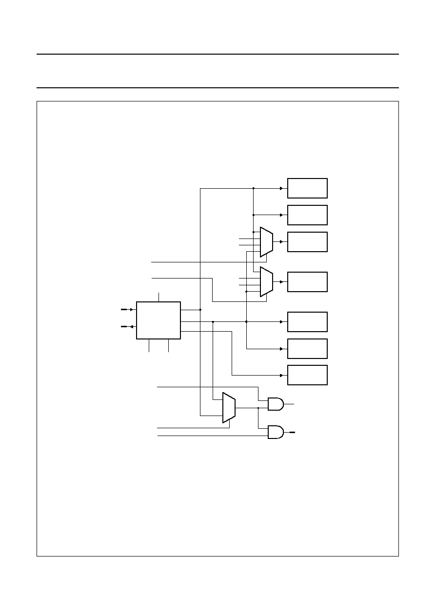
The microcontroller does not need a clock signal to run
instructions, because the CPU is built using the Philips
exclusive handshake technology. The peripheral blocks
however are connected to a clock for synchronization with
the outside world (e.g. MSK) or for a timed application (e.g.
Timer 2). The block related SFRs (peripheral function) are
therefore updated/modified with the applied clock. Two
prescalers (PSC1 and PSC2) are implemented which
allow the generation of two programmable clock signals
f
psc
and f
per
for internal usage.
Signal f
psc
from PSC1 is the default input clock of the timer
blocks. The complete timer functionality is specified in the
Section 6.5. Connected timers are the three 16-bit
timers Timer 0, 1 and 2 and the 8-bit Watchdog Timer.
The time interval of the connected timers can be adjusted
by programming of PSC1. The output frequency f
psc
can
be changed by selecting the division factor with the bits
PRESC.[2:0], (see Table 7).
All peripheral blocks, which require a clock signal: MSK,
and I
2
C-bus interface are connected to the clock signal
f
per
. PSC2 can be programmed by setting bits PRESC.4
and PRESC.3 (see Table 7). The choice of the division
factor must guarantee that all of the peripheral blocks are
within their specification, specially if an external clock
source of up to 12 MHz is applied.
Additionally Timer 1 and Timer 0 have a multiplexer on the
clock input to choose from 4 different clock sources.
The multiplexers are switched by setting user controllable
bits in the SYSCON SFR (bits 7 to 4). In the default setting
both timers are incrementing on the clock signal f
psc
coming from PSC1. Timer 1 and Timer 0 can however also
run on clock signal f
per
coming from PSC2. If used in the
proper way this flexibility on the timer input sources can
substantially contribute to a decrease in power
consumption. Ideas and tips to reduce power consumption
are given in Chapter 9.
The clock source of Timer 1 and Timer 0 can also be
switched to an external clock input signal T1 or T0 which
are multiplexed with one of the device input pins.
This mode is also functional even when there is no system
clock available. This means when a clock source is
supplied on a port pin Timer 1 or Timer 0 can count and
generate interrupts even when the chip is in Power-down
mode. More details are specified in Section 6.5.
The last multiplexer input to Timer 1 and Timer 0 is an
auxiliary mode which can be used to obtain the operation
speed from the handshake CPU. If this mode is activated
for the Timer 1 input source, the timer increments on every
ROM request. This means the timer increments by three
for a three byte instruction and by two for a two byte
instruction etc. If the auxiliary mode is activated for Timer 0
the timer increments on every instruction executed by
the CPU. This means the timer register holds the number
of instructions executed in a certain time frame. More
ideas and tips on how these clock source modes can be
used together with the handshake CPU can be found in
Chapter 9.
Table 3
Timer 1 input source select modes
Bits T1SRC[1:0] are defined in SYSCON SFR.
Table 4
Timer 0 input source select modes
Bits T0SRC[1:0] are defined in SYSCON SFR.
T1SRC1
T1SRC0
DESCRIPTION
0
0
f
psc
is the Timer 1 clock input
0
1
T1 is the Timer 1 clock input
1
0
the ROMreq signal is the Timer 1
clock input
1
1
f
per
is the Timer 1 clock input
T0SRC1
T0SRC0
DESCRIPTION
0
0
f
psc
is the Timer 0 clock input
0
1
T0 is the Timer 0 clock input
1
0
the InstrReq signal is the Timer 0
clock input
1
1
f
per
is the Timer 0 clock input
2001 Jun 19
11
Philips Semiconductors
Product specification
80C51 Ultra Low Power (ULP) telephony controller
P83CL882
handbook, full pagewidth
MGU266
WATCHDOG
TIMER
TIMER 2
TIMER 1
TIMER 0
OSCILLATOR
AND
COMPARATOR
XTAL1
T1SRC1/T1SRC0
T0SRC1/T0SRC0
XTAL2
ROMReq
T1
fpsc
MSK
MODEM
I
2
C-BUS
PORTS
fper
fosc
fosc
fpsc
InstrReq
T0
SELECT
XTM
power-down
to pin P1.4
CLKOUT
CPU
synchronisation
AUXSW
EXTCK
SYNC
AUXCLK
Fig.6 Clock overview.
2001 Jun 19
12
Philips Semiconductors
Product specification
80C51 Ultra Low Power (ULP) telephony controller
P83CL882
6.1.3.1
Prescaler Register (PRESC)
Reset value of PRESC SFR is XXX0 0000 (division factor 1 for PSC1 and PSC2).
Table 5
Prescaler Register (SFR address F3H)
Table 6
Description of PRESC bits
Table 7
Division factors for PSC1 and PSC2
6.1.4
A
UXILIARY CLOCK SIGNAL MODES
The 3 most significant bits in the Prescaler Register (see Tables 5 and 6) are used to enable additional clocking options.
A multiplexer is implemented (see Fig.6) to choose between f
psc
and f
per
as the source for AUXCLK. The multiplexer is
operated by bit AUXSW (PRESC.6). With bit EXTCK (PRESC.7) the AUXCLK is fed to pin P1.4 (CLKOUT) for external
use (initialize the port accordingly). Setting bit SYNC (PRESC.5) connects the AUXCLK to the instruction request input
of the CPU. In this way the CPU is synchronised to the clock and an instruction is executed at every clock pulse of
AUXCLK. In order to obtain exactly one instruction per clock cycle the period for AUXCLK must always be longer than
the length of the slowest instruction.
7
6
5
4
3
2
1
0
EXTCK
AUXSW
SYNC
PRESC.4
PRESC.3
PRESC.2
PRESC.1
PRESC.0
BIT
SYMBOL
DESCRIPTION
7
EXTCK
Switches AUXCLK to device pin P1.4 (CLKOUT).
6
AUXSW
Auxiliary Clock Switch. If AUXSW = 0; then AUXCLK equals f
psc
. If AUXSW = 1; then
AUXCLK equals f
per
.
5
SYNC
Switches the CPU to Synchronous mode.
4 to 0
PRESC.[4:0] These bits define the division factors for PSC1 and PSC2; see Table 7.
DIVISION FACTOR
PRESC.4
PRESC.3
PRESC.2
PRESC.1
PRESC.0
PSC2
(f
osc
/f
per
)
PSC1
(f
osc
/f
psc
)
1
-
0
0
X
X
X
2
-
0
1
X
X
X
4
-
1
0
X
X
X
8
-
1
1
X
X
X
-
1
X
X
0
0
0
-
2
X
X
0
0
1
-
4
X
X
0
1
0
-
6
X
X
0
1
1
-
8
X
X
1
0
0
-
10
X
X
1
0
1
-
12
X
X
1
1
0
-
16
X
X
1
1
1

2001 Jun 19
13
Philips Semiconductors
Product specification
80C51 Ultra Low Power (ULP) telephony controller
P83CL882
6.1.5
S
YSTEM
C
ONTROL
R
EGISTER
(SYSCON)
Table 8
System Control Register (SFR address B4H)
Table 9
Description of SYSCON bits
7
6
5
4
3
2
1
0
T1SRC1
T1SRC0
T0SRC1
T0SRC0
-
-
SELECT
XTM
BIT
SYMBOL
DESCRIPTION
7
T1SRC1
These 2 bits select the clock source for Timer 1; see Table 3.
6
T1SRC0
5
T0SRC1
These 2 bits select the clock source for Timer 0; see Table 4.
4
T0SRC0
3
-
do not use
2
1
SELECT
comparator select bit; see Table 2
0
XTM
oscillator disable bit; see Table 2
2001 Jun 19
14
Philips Semiconductors
Product specification
80C51 Ultra Low Power (ULP) telephony controller
P83CL882
6.2
The CPU
6.2.1
G
ENERAL
Ultra Low Power (ULP), points to the special 80C51 CPU
architecture used in this device allowing significant power
saving.
The CPU of the P83CL882 is realized in the Philips
exclusive asynchronous handshaking technology, which is
completely different to usual implementations of this core.
The processor does not need a clock signal to run
instructions. Every function within the CPU is self timed
and always runs at the maximum speed that the silicon die
under the current operating conditions allows (supply
voltage and temperature). The advantage is the
combination of a high computing power with reduced
average power consumption and low EMC noise
generation. Details about speed and energy consumption
per instruction can be found in Chapter 8.
Summary of the CPU features:
∑
No CPU clock is needed
∑
Only useful bytes are fetched from the program
memory; the dummy read cycles which exist in the
standard 80C51 have been eliminated to save power
∑
To further speed up the program execution; there is
always a pre-fetch of the next byte of code from memory
during the execution of the current instruction; in the
case of a jump the pre-fetched byte is discarded
∑
In Idle mode the CPU power is reduced to leakage; only
the enabled peripheral blocks consume power but can
be switched off independently
∑
The only need for a clock is as a timing reference for
timers/counters and to generate the timing for the
I/O lines to synchronise with the off-chip world.
6.2.2
R
ESET OPERATION
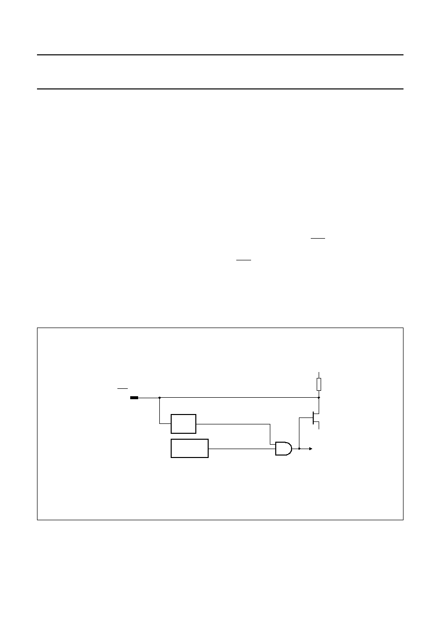
There are two possibilities to reset the CPU (see Fig.7):
∑
Watchdog Timer reset
∑
External reset via I/O pin RST.
If an internal reset is executed (Watchdog Timer), the reset
pin RST will be pulled to ground which can be used as
reset signal for other ICs. The reset pin is LOW for at least
1024 clock cycles, and released 16 clock cycles prior to
first code fetch (see Figs 8 and 9).
handbook, full pagewidth
internal
reset
WATCHDOG
TIMER
Rpu
VSS
VDD
RST
(external
reset)
LOGIC
MGU267
Fig.7 Reset sources.

2001 Jun 19
15
Philips Semiconductors
Product specification
80C51 Ultra Low Power (ULP) telephony controller
P83CL882
6.2.2.1
Watchdog Timer reset
If the Watchdog Timer expires, it will trigger a reset.
MGT287
Watchdog
Timer
1024 clocks
16 clocks
CPU start
RST
output
CPU
activity
Fig.8 Watchdog Timer reset timing.
2001 Jun 19
16
Philips Semiconductors
Product specification
80C51 Ultra Low Power (ULP) telephony controller
P83CL882
6.2.2.2
External reset via RST
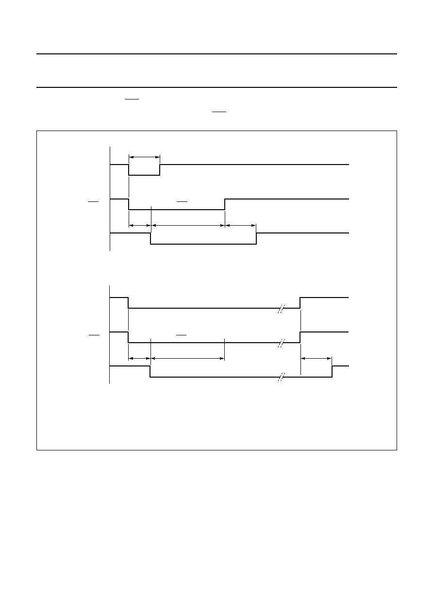
An external device can cause a chip reset, if the reset pin RST is pulled to ground.
MGT546
RST by counter
maximum 16384 = 2
14
clocks
16 clocks
8 clocks
RST
CPU
activity
External
applied
MGT286
RST by counter
maximum 16384 = 2
14
clocks
16 clocks
8 clocks
RST
CPU
activity
minimum
8 clocks
External
applied
Fig.9 External reset.
a. Short external reset.
b. Long external reset.

2001 Jun 19
17
Philips Semiconductors
Product specification
80C51 Ultra Low Power (ULP) telephony controller
P83CL882
6.2.3
I
DLE AND
P
OWER
-
DOWN OPERATION
Idle and Power-down are power saving modes of the
microcontroller that can be activated when no CPU activity
is required. These two modes are extremely useful for the
asynchronous CPU, because they offer the possibility to
profit from the speed of the CPU and to save power as
soon as the task is finished. Idle mode stops the code
execution of the CPU, but the internal oscillator remains
active, and also all peripheral functions connected to the
on-chip clock signal. Unused blocks can be switched off
independently. However, during Power-down mode the
clock oscillator is stopped and therefore also all peripheral
blocks will stop their activity.
6.2.3.1
Idle mode
The following functions remain active during Idle mode:
∑
Timers 0, 1 and 2
∑
Wake-up counter
∑
Watchdog Timer counter
∑
MSK modem
∑
I
2
C-bus interface
∑
External interrupt.
The instruction that sets PCON.0 (PCON SFR) is the last
instruction executed in the normal operating mode before
the Idle mode is activated. The RAM and all of the registers
are preserved and maintain their data during Idle mode:
the CPU status, the stack pointer, program counter,
program status word and accumulator.
There are two ways to terminate the Idle mode:
∑
Activation of any enabled interrupt will cause PCON.0 to
be cleared by hardware thus terminating the Idle mode.
The interrupt is serviced, and following the RETI
instruction, the next instruction to be executed will be the
one following the instruction that put the device in the
Idle mode.
∑
The second way of terminating the Idle mode is with an
internal or external hardware reset. Reset redefines all
SFRs but does not affect the on-chip RAM. The source
of an internal reset is the Watchdog Timer if the preset
delay has expired.
6.2.3.2
Power-down mode
The instruction that sets PCON.1 (PCON SFR) is the last
instruction executed in the normal operating mode before
the Power-down mode is activated. During Power-down
mode, the RAM and all of the registers maintain their data:
the CPU status, the stack pointer, program counter,
program status word and accumulator.
There are two ways to terminate the Power-down mode:
∑
Activation of any of the interrupts listed below will cause
PCON.1 to be cleared by hardware thus terminating the
Power-down mode. The interrupt is serviced, and
following the RETI instruction, the next instruction to be
executed will be the one following the instruction that put
the device in the Power-down mode. Interrupts which
can generate a wake-up from power-down:
≠ External interrupts (INT0 to INT9)
≠ Timer 0 and Timer 1: only when pins T0 and T1 are
used as the external timer source input (SYSCON
SFR bits 7 to 4)
∑
The second way of terminating the Power-down mode is
with an internal or external hardware reset. Reset does
not affect the on-chip RAM, but all SFRs are set to the
default value.

2001 Jun 19
18
Philips Semiconductors
Product specification
80C51 Ultra Low Power (ULP) telephony controller
P83CL882
6.2.3.3
Power Control Register (PCON)
The reduced power modes are activated by software using this special function register. PCON is not bit addressable.
The reset value of PCON = 0000 0000.
Table 10 Power Control Register (SFR address 87H)
Bits PCON[7:2] are reserved and must be kept to logic 0.
Table 11 Reduced power modes selection
6.2.4
CPU
START
-
UP TIMING
6.2.4.1
CPU start-up after reset
Three possibilities on how the CPU can start executing code after a reset phase are described below.
When the CPU is triggered to wake-up after a power-on reset (see Fig.8), the clock oscillator usually needs some time
to ramp up. To allow the oscillator to stabilize the CPU contains a down counter for a fixed delay of 1024 + 16 clock
cycles. After this delay the CPU starts with code execution.
When CPU start-up is initiated from an external reset (see Fig.9), the down counter is not initialized and the time between
reset going active and first code execution can be maximum 16400 clock cycles.
When a CPU start-up is after a Watchdog Timer reset (see Fig.8), the RST pin will be pulled low for 1024 clock cycles.
Another 16 clocks later the CPU will start executing code.
6.2.4.2
CPU start-up after power-down
After wake-up from Power-down mode (see Fig.10) the user has the possibility to shorten the start-up time by
programming the Wake-up Counter Register (WKCON). This can be useful when an external clock source is used
instead of the on-chip oscillator, or when the accuracy of the time reference is not needed immediately after a restart.
This feature enables power saving and fast wake-up in applications where the CPU frequently goes into Power-down
mode. The wake-up delay can be calculated as shown in Table 13.
7
6
5
4
3
2
1
0
0
0
0
0
0
0
PD
IDL
PD
IDL
DESCRIPTION
0
0
CPU running
0
1
activates the Idle mode
1
0
activates the Power-down mode
1
1

2001 Jun 19
19
Philips Semiconductors
Product specification
80C51 Ultra Low Power (ULP) telephony controller
P83CL882
6.2.5
W
AKE
-
UP
C
OUNTER
R
EGISTER
(WKCON)
Table 12 Wake-up Counter Register (SFR address DDH)
Table 13 Description of WKCON bits
7
6
5
4
3
2
1
0
WKCON.7
WKCON.6
WKCON.5
WKCON.4
WKCON.3
WKCON.2
WKCON.1
WKCON.0
BIT
SYMBOL
DESCRIPTION
7 to 0
WKCON.[7:0]
The wake-up delay can be calculated as follows: Wake-up
delay = (1024
-
4)
◊
WKCON. Where WKCON is the content of the
Wake-up Counter Register.
WKCON = 00H: (default) wake-up delay = 1024 clocks
WKCON = CCH: wake-up delay = 208 clocks
WKCON = FFH: wake-up delay = 4 clocks.
MGT288
wake-up
event
programmable delay
oscillator stop
CPU
activity
CPU start
CLOCK
CPU stop
start
unstable clock
Fig.10 Wake-up timing from power-down.

2001 Jun 19
20
Philips Semiconductors
Product specification
80C51 Ultra Low Power (ULP) telephony controller
P83CL882
6.3
Interrupt controller
In order to service interrupt requests coming from external
events and from the on-chip peripherals the P83CL882
offers a 17 source, two priority level nested interrupt
system. A detailed description of the interrupt process is
given in the following sections. Table 14 shows the
available interrupts with each vector address and Table 15
shows an overview of all the interrupt related SFRs. The
detailed interrupt related SFR description can be found in
Sections 6.3.4 to 6.3.10.
6.3.1
G
ENERAL
Each interrupt vector points to a separate location in
program memory for its service routine. Each source can
be individually enabled or disabled by its corresponding bit
in the Interrupt Enable Registers (IEN0, IEN1 and IEN2).
The priority level is selected via the Interrupt Priority
Registers (IP0, IP1 and IP2). All available interrupts can be
globally disabled or enabled.
The interrupt controller samples all active sources during
one instruction cycle. Evaluation of the interrupts is then
performed. A priority decoder decides which interrupt is
serviced. Each interrupt has its own vector pointing to an
8 bytes long memory segment.
A low priority interrupt can be interrupted by a high priority
interrupt, but not by another low priority interrupt i.e. only
two interrupt levels are possible.
Between the RETI instruction (Return from Interrupt) and
the execution of a next interrupt at least one instruction of
the lower program level is executed. The interrupt service
with different priorities is shown in Fig.11.
An interrupt is performed with a long subroutine call
(LCALL) to a vector address, which is determined by the
respective interrupt. During LCALL the Program
Counter (PC) is pushed onto the stack. Returning from
interrupt with RETI, the PC is popped from the stack.
In the event of several interrupts with the same priority
level, the order of sequence in which they will be serviced
is determined by the scanning order.
The interrupt highest in the scanning list will always be
served first, interrupts lower in the scanning list will be
served in the order as shown in Fig.12. No interrupt will be
lost.
Table 14 Available interrupts (ordered by vector address)
HW = hardware; SW = software.
SOURCE
SYMBOL
VECTOR
(HEX)
CLEARED
BY
INT 0
X0
0003
HW
Timer 0
T0
000B
HW
INT 1
X1
0013
HW
Timer 1
T1
001B
HW
I
2
C-bus
S1
002B
SW
Timer 2
T2
0033
SW
INT2
X2
003B
SW
INT3
X3
0043
SW
INT4
X4
004B
SW
INT5
X5
0053
SW
INT6
X6
005B
SW
INT7
X7
0063
SW
INT8
X8
006B
SW
INT9
X9
0073
SW
MSK modem
transmitter
MTI
0083
SW
MSK mode receiver
MRI
008B
SW
Watchdog Timer
WDI
00B3
SW
2001 Jun 19
21
Philips Semiconductors
Product specification
80C51 Ultra Low Power (ULP) telephony controller
P83CL882
Table 15 Interrupt related SFRs
SFR
DESCRIPTION
SFR ADDRESS
RESET VALUE
IEN0
interrupt enable register 0
A8H
0000 0000
IEN1
interrupt enable register 1 (INT2 to INT9)
E8H
0000 0000
IEN2
interrupt enable register 2
F1H
0000 0000
IP0
interrupt priority register 0
B8H
0000 0000
IP1
interrupt priority register 1 (INT2 to INT9)
F8H
0000 0000
IP2
interrupt priority register 2
F9H
0000 0000
IX1
external interrupt polarity register 1
E9H
0000 0000
ISE1
external interrupt sensitivity register 1
E1H
0000 0000
IRQ1
external interrupt request flag register 1
C0H
0000 0000
handbook, full pagewidth
MGR125
Interrupt level 2x
Interrupt level 1
Program level 0
RETI
Level 21
RETI
Level 20
RETI
one
instruction
IP = 1
IP = 1
IP = 0
Fig.11 Interrupt hierarchy.

2001 Jun 19
22
Philips Semiconductors
Product specification
80C51 Ultra Low Power (ULP) telephony controller
P83CL882
X0
X5
MRI
T0
T2
S1
X6
MTI
X1
X2
X7
T1
X3
X8
X4
X9
WDI
IEN0
IEN1
IEN2
IP0
IP1
IP2
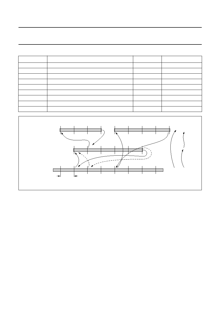
INTERRUPT
SOURCES
decreasing
priority
within same
level
HIGH
LOW
MGU259
Fig.12 Interrupt assignment and priorities (listed by scanning order).

2001 Jun 19
23
Philips Semiconductors
Product specification
80C51 Ultra Low Power (ULP) telephony controller
P83CL882
6.3.2
I
NTERRUPT PROCESS
1. Sample the interrupt lines. The interrupt lines are
latched at the beginning of each instruction cycle.
2. Analyse the requests. The sampled interrupt lines
will be analysed with respect to the relevant Interrupt
Enable Register (IENx) and Interrupt Priority
Register (IPx). The process will deliver the vector of
the highest interrupt request and the priority
information. Depending on the interrupt level and the
priority of the interrupt in progress, an interrupt request
to the core is performed. The vector address will be
passed to the core process.
3. Interrupt request to core.
a) Level 0: the interrupt request to the core is
performed, when at least one instruction is
performed since the RETI from Level 1.
b) Level 1: the interrupt request is performed, when
at least one instruction is performed since the RETI
from Level 21 and the request has high priority.
c) Level 20: no request is performed.
d) Level 21: no request is performed.
4. Update the interrupt level.
a) Level 0: in the event of a high priority interrupt the
new level will be Level 20; if it is a low priority
interrupt, the new level will be Level 1.
b) Level 1: in the event of a high priority interrupt, the
new level will be Level 21; a low priority interrupt is
not performed, the level is unchanged; on RETI the
new level will be Level 0.
c) Level 20: on RETI; the new level is Level 0.
d) Level 21: on RETI; the new level is Level 1.
e) Level 1: on RETI; the new level is Level 0.
f) Level 0: the new level is Level 0.
5. Clearing the flags. During the forced LCALL the
interrupt flag of the relevant interrupt is cleared by
hardware, if applicable, otherwise by software.
6. Idle and Power-down. When Idle (PCON.0) or
Power-down (PCON.1) is set, the interrupt controller
waits for the wake-up signal. Because the interrupt
controller is waiting for wake-up, all activity in the
circuit will be stopped, thus no handshake can be
completed. The wake-up signal for Idle is the OR of all
the interrupt request bits and the reset. For
Power-down the wake-up signal is built only with the
Port 1 external interrupt request flags (X2 to X9) and
the reset (external reset).
6.3.3
P
ORT
1
INTERRUPTS
Eight Port 1 lines can be used as external interrupt inputs
(X2 to X9). When enabled by IEN1 SFR, each of these
interrupts may wake-up the device from Idle or
Power-down. These external interrupts can each
independently be programmed to positive and negative
polarity and to edge and level sensitivity by setting SFR
IX1 and ISE1 (see Table 34). Figure 12 shows
programming of polarity and sensitivity of the Port 1
interrupts. When a valid event occurs on an enabled Port 1
interrupt, the corresponding bit in the Interrupt Request
Flags Register will be set (IRQ1). The interrupt request
flags must be cleared by software.

2001 Jun 19
24
Philips Semiconductors
Product specification
80C51 Ultra Low Power (ULP) telephony controller
P83CL882
6.3.4
I
NTERRUPT
E
NABLE
R
EGISTER
0 (IEN0)
Table 16 Interrupt Enable Register 0 (SFR address A8H)
Table 17 Description of IEN0 bits
Logic 0 = interrupt disabled; logic 1 = interrupt enabled.
6.3.5
I
NTERRUPT
E
NABLE
R
EGISTER
1 (IEN1)
Table 18 Interrupt Enable Register 1 (SFR address E8H)
Table 19 Description of IEN1 bits
Logic 0 = interrupt disabled; logic 1 = interrupt enabled.
7
6
5
4
3
2
1
0
EA
ET2
ES1
-
ET1
EX1
ET0
EX0
BIT
SYMBOL
DESCRIPTION
7
EA
General enable/disable control. If EA = 0, no interrupt is enabled; if EA = 1, any
individually enabled interrupt will be accepted.
6
ET2
enable T2 interrupt
5
ES1
enable I
2
C-bus interrupt
4
-
reserved
3
ET1
enable Timer 1 interrupt (T1)
2
EX1
enable external interrupt 1
1
ET0
enable Timer 0 interrupt (T0)
0
EX0
enable external interrupt 0
7
6
5
4
3
2
1
0
EX9
EX8
EX7
EX6
EX5
EX4
EX3
EX2
BIT
SYMBOL
DESCRIPTION
7
EX9
enable external interrupt 9
6
EX8
enable external interrupt 8
5
EX7
enable external interrupt 7
4
EX6
enable external interrupt 6
3
EX5
enable external interrupt 5
2
EX4
enable external interrupt 4
1
EX3
enable external interrupt 3
0
EX2
enable external interrupt 2
2001 Jun 19
25
Philips Semiconductors
Product specification
80C51 Ultra Low Power (ULP) telephony controller
P83CL882
6.3.6
I
NTERRUPT
E
NABLE
R
EGISTER
2 (IEN2)
Table 20 Interrupt Enable Register 2 (SFR address F1H)
Table 21 Description of IEN2 bits
Logic 0 = interrupt disabled; logic 1 = interrupt enabled.
6.3.7
I
NTERRUPT
P
RIORITY
R
EGISTER
0 (IP0)
Table 22 Interrupt Priority Register 0 (SFR address B8H)
Table 23 Description of IP0 bits
Logic 0 = low priority; logic 1 = high priority.
7
6
5
4
3
2
1
0
EWDI
-
-
-
-
-
EMTI
EMRI
BIT
SYMBOL
DESCRIPTION
7
EWDI
enable Watchdog Timer interrupt
6
-
reserved
5
-
reserved
4
-
reserved
3
-
reserved
2
-
reserved
1
EMTI
enable MSK transmitter interrupt
0
EMRI
enable MSK receiver interrupts
7
6
5
4
3
2
1
0
-
PT2
PS1
-
PT1
PX1
PT0
PX0
BIT
SYMBOL
DESCRIPTION
7
-
reserved
6
PT2
Timer 2 interrupt priority level
5
PS1
I
2
C-bus interrupt priority level
4
-
reserved
3
PT1
Timer 1 interrupt priority level
2
PX1
external interrupt 1 priority level
1
PT0
Timer 0 interrupt priority level
0
PX0
external interrupt 0 priority level

2001 Jun 19
26
Philips Semiconductors
Product specification
80C51 Ultra Low Power (ULP) telephony controller
P83CL882
6.3.8
I
NTERRUPT
P
RIORITY
R
EGISTER
1 (IP1)
Table 24 Interrupt Priority Register 1 (SFR address F8H)
Table 25 Description of IP1 bits
Logic 0 = low priority; logic 1 = high priority.
6.3.9
I
NTERRUPT
P
RIORITY
R
EGISTER
2 (IP2)
Table 26 Interrupt Priority Register 2 (SFR address F9H)
Table 27 Description of IP2 bits
Logic 0 = low priority; logic 1 = high priority.
7
6
5
4
3
2
1
0
PX9
PX8
PX7
PX6
PX5
PX4
PX3
PX2
BIT
SYMBOL
DESCRIPTION
7
PX9
external interrupt 9 priority level
6
PX8
external interrupt 8 priority level
5
PX7
external interrupt 7 priority level
4
PX6
external interrupt 6 priority level
3
PX5
external interrupt 5 priority level
2
PX4
external interrupt 4 priority level
1
PX3
external interrupt 3 priority level
0
PX2
external interrupt 2 priority level
7
6
5
4
3
2
1
0
PWDI
-
-
-
-
-
PMTI
PMRI
BIT
SYMBOL
DESCRIPTION
7
PWDI
Watchdog Timer interrupt priority level
6
-
reserved
5
-
reserved
4
-
reserved
3
-
reserved
2
-
reserved
1
PMTI
MSK transmitter interrupt priority level
0
PMRI
MSK receiver interrupt priority level
2001 Jun 19
27
Philips Semiconductors
Product specification
80C51 Ultra Low Power (ULP) telephony controller
P83CL882
6.3.10
I
NTERRUPT
R
EQUEST
F
LAG
R
EGISTER
1 (IRQ1)
Table 28 Interrupt Request Flag Register 1 (SFR address C0H)
Table 29 Description of IRQ1 bits
6.3.11
I
NTERRUPT POLARITY AND
S
ENSITIVITY REGISTERS
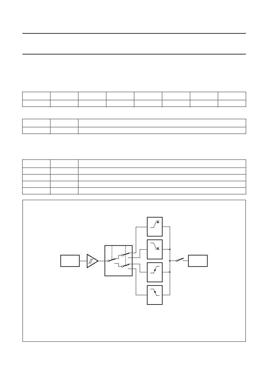
6.3.11.1
Interrupt Polarity Register 1 (IX1)
Writing either a logic 1 or logic 0 to any Interrupt Polarity Register bit sets the polarity of the corresponding external
interrupt. If the interrupt sensitivity bit (ISE1 register, Section 6.3.11.2) is set to `level' sensitive then a logic 1 corresponds
to active HIGH level and logic 0 to active LOW level. If the ISE1 register is set to `edge' sensitive then a logic 1
corresponds to a rising edge and a logic 0 to a falling edge. See also Table 34 and Fig.12.
Table 30 Interrupt Polarity Register 1 (SFR address E9H)
Table 31 Description of IX1 bits
7
6
5
4
3
2
1
0
IQ9
IQ8
IQ7
IQ6
IQ5
IQ4
IQ3
IQ2
BIT
SYMBOL
DESCRIPTION
7
IQ9
external interrupt 9 request flag
6
IQ8
external interrupt 8 request flag
5
IQ7
external interrupt 7 request flag
4
IQ6
external interrupt 6 request flag
3
IQ5
external interrupt 5 request flag
2
IQ4
external interrupt 4 request flag
1
IQ3
external interrupt 3 request flag
0
IQ2
external interrupt 2 request flag
7
6
5
4
3
2
1
0
IX9
IX8
IX7
IX6
IX5
IX4
IX3
IX2
BIT
SYMBOL
DESCRIPTION
7 to 0
IX9 to IX2
external interrupt 9 to 2 polarity level
2001 Jun 19
28
Philips Semiconductors
Product specification
80C51 Ultra Low Power (ULP) telephony controller
P83CL882
6.3.11.2
Interrupt Sensitivity Register 1 (ISE1)
Writing either a logic 1 or logic 0 to an Interrupt Sensitivity Register bit sets the type of the corresponding external
interrupt to edge sensitive (logic 1) or level sensitive (logic 0).
Table 32 Interrupt Sensitivity Register 1 (SFR address E1H)
Table 33 Description of ISE1 bits
6.3.11.3
Interrupt polarity and sensitivity options
Table 34 Interrupt polarity and sensitivity options
`n' denotes the bit position in the SFRs IX1 and ISE1.
7
6
5
4
3
2
1
0
ISE9
ISE8
ISE7
ISE6
ISE5
ISE4
ISE3
ISE2
BIT
SYMBOL
DESCRIPTION
7 to 0
ISE9 to ISE2 external interrupt 9 to 2 sensitivity
IX1.n
ISE1.n
DESCRIPTION
0
0
LOW-level sensitive
1
0
HIGH-level sensitive
0
1
falling edge sensitive
1
1
rising edge sensitive
MGT290
P1.n
PORT1
ISE1.n
IX1.n
negative
level
positive
edge
IRQ1.n
IEN1.n
positive
level
negative
edge
Fig.13 Polarity and sensitivity of Port 1 interrupts.

2001 Jun 19
29
Philips Semiconductors
Product specification
80C51 Ultra Low Power (ULP) telephony controller
P83CL882
6.4
Port control logic
Four 8-bit I/O ports are implemented in the device. Some
of these general purpose I/Os are multiplexed with
alternative functions. Port 0 is the only port with no
multiplexed alternative functions. Port 3 and a part of
Port 1 are multiplexed with analog functions. Every port bit
can be independently configured in 4 different modes.
6.4.1
P
ORT FUNCTIONALITY
Port 0 8-bit bidirectional I/O port with no alternative
functions. Every port pin can be used as
open-drain, standard port, high-impedance input or
push-pull output. Port 0 is used during emulation
mode.
Port 1 8-bit bidirectional I/O port with alternative functions.
Every port, except P1.6 and P1.7 can be used as
open-drain, standard port, high-impedance input or
push-pull output.
∑
P1.0 to P1.7 provides the inputs for the external
interrupts INT2 to INT9; the interrupts are
enabled by selecting the proper bit in the
interrupts enable register
∑
P1.1 and P1.2 provide the Timer 2 external
trigger input (T2EX) and the Timer 2 external
count input (T2)
∑
P1.4 provides the clock output CLKOUT
(f
psc
or f
per
)
∑
P1.5 provide the Timer 2 clock output of the
clock-output mode (T2OUT); to enable output the
data SFR must contain logic 1s
∑
P1.6 and P1.7 provide the I
2
C-bus clock and
data I/O, SCL and SDA. P1.6 and P1.7 can only
be configured as open-drain output or
high-impedance input; there is no clamp diode to
V
DD
. I
2
C-bus signals are connected to the port if
bit ENS1 (S1CON SFR) is set to logic 1.
Port 2 Not used.
Port 3 8-bit bidirectional I/O port with alternative functions.
Every port can be used as open-drain, standard
port, high-impedance input or push-pull output.
∑
P3.0 to P3.2 provide the MSK output signals
MOUT0, MOUT1 and MOUT2
∑
P3.4 also provides the Timer 0 external clock
input
∑
P3.5 also provides the Timer 1 external clock
input.
6.4.2
P
ORT
I/O
CONFIGURATION
Each port bit consists of a data latch, two configuration
latches, an output driver and an input buffer. The I/O port
configurations are determined by the settings in the port
configuration SFRs, PnCFGA and PnCFGB, where `n'
indicates the specific port number (0, 1, 3 and 4). The
combination of 2 bits in each of the 2 configuration SFRs
relates to the output setting for the corresponding port pin,
allowing any combination of the 4 I/O modes to be mixed
on those port pins. The port I/O configuration types are
shown in Fig.14 and described in
Sections 6.4.2.1 to 6.4.2.4.
6.4.2.1
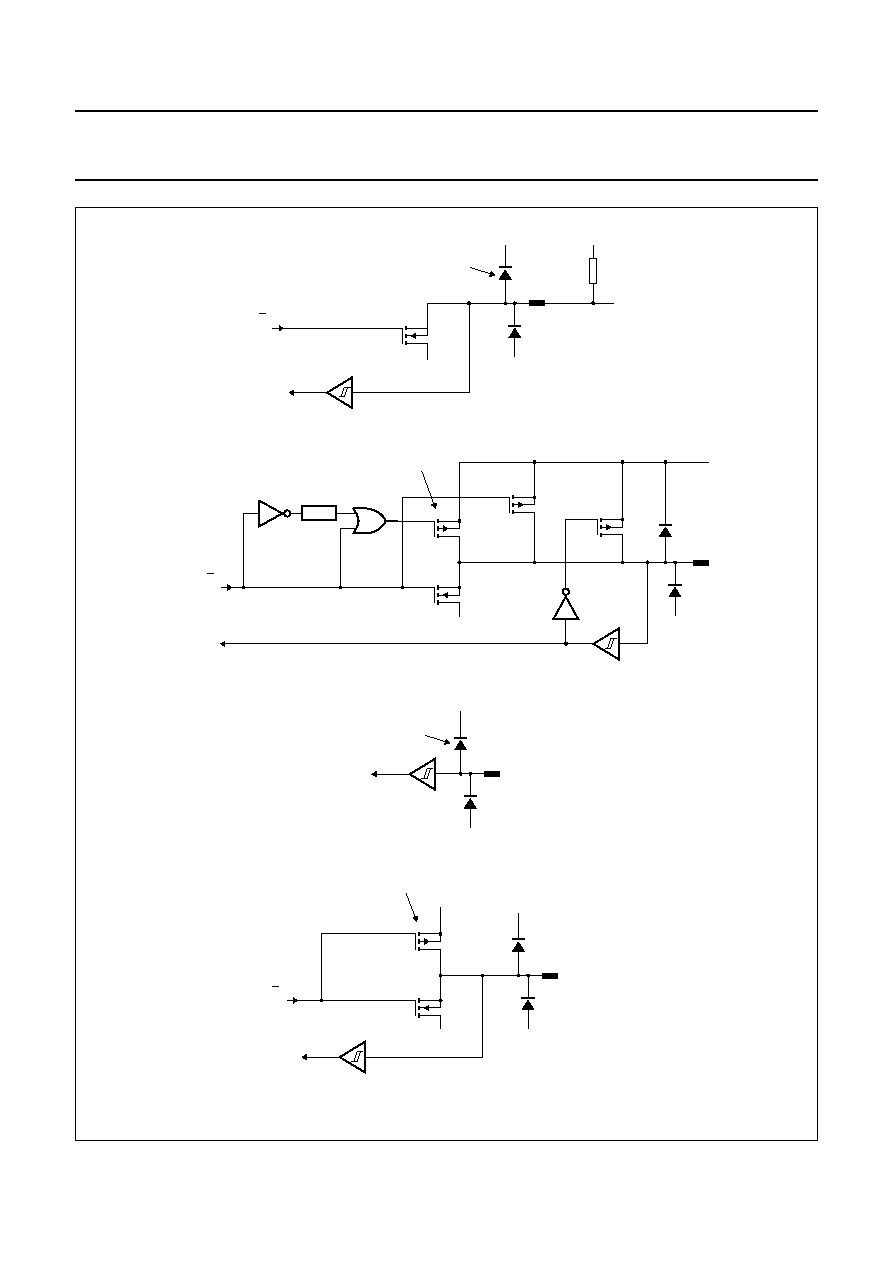
Open-drain
Quasi-bidirectional I/O with n-channel open-drain output.
Use as an output requires the connection of an external
pull-up resistor; all pins have ESD protection diodes
against V
DD
and V
SS
, except for the I
2
C-bus pins P1.6 and
P1.7, which have no ESD protection to V
DD
.
6.4.2.2
Standard port
Quasi-bidirectional I/O with pull-up; the strong pull-up `p1'
is turned on for three clock (f
osc
) edges after a
LOW-to-HIGH transition in the port latch; after these three
clock edges the port is only weakly driven through `p2' and
`very weakly' driven through `p3' (see Fig.14b).
6.4.2.3
High-impedance input
This mode turns off all output drivers on a port. The pin will
not source or sink current and may be used as an
input-only pin. (see Fig.14c). In order not to increase the
current consumption the high-impedance input should not
float.
6.4.2.4
Push-pull
Output with drive capability in both polarities; under this
mode, pins can only be used as outputs (see Fig.14d).

2001 Jun 19
30
Philips Semiconductors
Product specification
80C51 Ultra Low Power (ULP) telephony controller
P83CL882
Table 35 Port I/O configuration types
`n' indicates the specific port number (0, 1, 3 and 4).
Table 36 Reset state of port related SFRs
Note
1. This means all ports, except P0.2, P0.3, P0.4, P1.6 and P1.7 are initialized in standard port configuration driving a
weak logic 1. Port 0.2 and P0.3 are initialised as open-drain outputs, floating. P0.4 is initialised as bidirectional,
driving a strong logic 0. I
2
C-bus I/Os P1.6 and P1.7 are initialised in open-drain configuration, floating. The
configuration registers (P1CFGA.7 to 6 and P1CGB.7 to 6) are however configured as standard port configuration
but the connections to the port PMOS transistors are not present.
TYPE
PnCFGA
PnCFGB
NORMAL PORTS
I
2
C-BUS PORTS
Open-drain
0
0
open-drain
open-drain
Standard port
1
0
quasi-bidirectional
open-drain
High-impedance input
0
1
high-impedance input
high-impedance input
Push-pull
1
1
push-pull
open-drain
SFR
DESCRIPTION
SFR ADDRESS
(HEX)
STATE AFTER RESET
(1)
P0
Port 0 output data
80
1110 1111
P0CFGA
Port 0 Configuration A
8E
1111 0011
P0CFGB
Port 0 Configuration B
8F
0000 0000
P1
Port 1 output data
90
1111 1111
P1CFGA
Port 1 Configuration A
9E
1111 1111
P1CFGB
Port 1 Configuration B
9F
0000 0000
P3
Port 3 output data
B0
1111 1111
P3CFGA
Port 3 Configuration A
BE
1111 1111
P3CFGB
Port 3 Configuration B
BF
0000 0000
2001 Jun 19
31
Philips Semiconductors
Product specification
80C51 Ultra Low Power (ULP) telephony controller
P83CL882
handbook, full pagewidth
MBK004
this diode is not
implemented
on the I
2
C-bus pins
VSS
VDD external
n
Q
from port latch
external
pull-up
I/O pin
input data
VDD
VSS
handbook, full pagewidth
MBK001
p1
p2
p3
input data
1 oscillator
period
n
VSS
VDD
strong pull-up
I/O pin
Q
from port latch
IN1
VSS
handbook, full pagewidth
MBK002
this diode is not
implemented
on the I
2
C-bus pins
input data
VDD
I/O pin
VSS
handbook, full pagewidth
MBK003
p
n
strong pull-up
Q
from port latch
VSS
VDD
VDD
I/O pin
input data
VSS
Fig.14 Port configuration options.
a. Open-drain.
b. Standard/quasi-bidirectional.
c. High-impedance input.
d. Push-pull.

2001 Jun 19
32
Philips Semiconductors
Product specification
80C51 Ultra Low Power (ULP) telephony controller
P83CL882
6.5
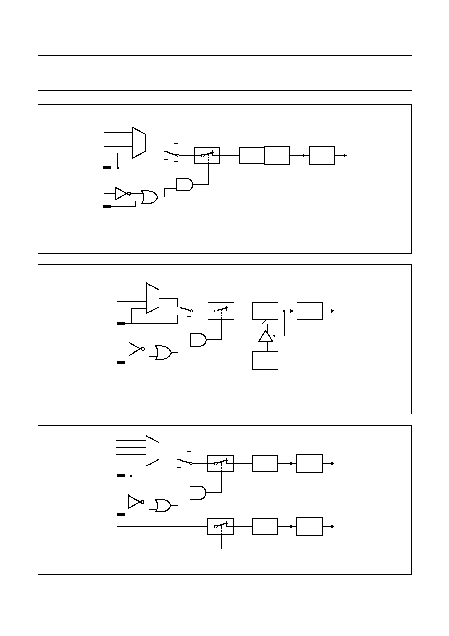
Timer 0 and Timer 1 event counters
Timer 0 and Timer 1 can perform the following functions:
∑
Measure time intervals and pulse durations
∑
Count events
∑
Measure CPU speed
∑
Generate interrupt requests.
Timer 0 and Timer 1 can be programmed independently to
operate in four modes:
Mode 0 8-bit timer or 8-bit counter each with divide-by-32
prescaler.
Mode 1 16-bit time interval or event counter.
Mode 2 8-bit time interval or event counter with automatic
reload upon overflow.
Mode 3 Timer 1 stopped and Timer 0 operates as two
separate counters.
A block diagram of Timer 0 and Timer 1 with possible clock
sources is shown in Fig.15.
Table 37 Timer/counter 0 and Timer/counter 1 related SFRs
SFR
DESCRIPTION
SFR ADDRESS
RESET VALUE
TCON
Timer/counter 0 and Timer/counter 1 Control Register
88H
0000 0000
TMOD
Timer/counter 0 and 1 Mode Control Register
89H
0000 0000
SYSCON
System Control Register
B4H
0000 0000
MGT292
C/T = 0
C/T = 1
TL1
TH1
TH0
C/T = 0
C/T = 1
TL0
T0
TR0
control
GATE
INT0
T1
TR1
GATE
INT1
ROMReq
fper
fpsc
InstrReq
fper
fpsc
control
Fig.15 Timer/counter 0 and 1; clock sources and control logic.

2001 Jun 19
33
Philips Semiconductors
Product specification
80C51 Ultra Low Power (ULP) telephony controller
P83CL882
6.5.1
C
LOCK SOURCE SIGNALS OF
T
IMER
0
AND
T
IMER
1
In all four modes Timer 0 and Timer 1 can be configured to
increment from different internal and external clock
sources. The TMOD and SYSCON registers must be
written to determine the source of the clock signal. After
reset the clock source for both timers is connected to the
internal clock signal from PSC1 (f
psc
). The second of four
possible clock sources is connected to the other internal
clock signal coming from PSC2 (f
per
).
The clock input on both timers has a multiplexer to choose
from 4 different clock sources. If the multiplexers are
switched to another input by setting user controllable bits
in the SYSCON SFR (bits 7 to 4), the timers can also
increment on the other on-chip clock signal coming from
PSC2 (f
per
).
In counter mode the timers are incrementing on transitions
on the T0 and T1 input pins. First way to enter this mode
is by setting control bits C/T (TMOD.6 and 2). Second way
is to configure SYSCON to switch the input multiplexer to
the clock input signal T1 or T0 while C/T is logic 0. The
latter is also functional even when there is no system clock
available. This means when a clock source is supplied on
a port pin the Timer 1 or 0 can count and generate
interrupts even when the chip is in Power-down mode.
Maximum input signal frequency and duty cycle for the
timer in counter mode is given in Chapter 11.
The last multiplexer input to Timer 1 and Timer 0 is an
auxiliary mode which can be used to obtain the operation
speed from the handshake CPU. If this mode is activated
for the Timer 1 input source, the timer increments on every
ROM request. This means the timer increments by three
for a three byte instruction and by two for a two byte
instruction etc. If the auxiliary mode is activated for Timer 0
the timer increments on every instruction executed by
the CPU. This means the timer register holds the number
of instructions executed in a certain time frame. This can
be used to obtain the number of Mips at which the
processor is running. The SYSCON register is described
in Section 6.5.5.
6.5.2
O
PERATING MODES OF
T
IMER
0
AND
T
IMER
1
The `Timer' or `Counter' function is selected by control
bits C/T in the Special Function Register TMOD. These
two Timer/Counters have four operating modes, which are
selected by bit-pairs (M1 and M0) in TMOD.
Modes 0, 1, and 2 are the same for both Timers/Counters.
Mode 3 configures Timer 0 while Timer 1 is disabled.
The four operating modes are:
Mode 0 Putting either Timer 0 or Timer 1 into Mode 0
makes it look like an 8048 timer, which is an 8-bit
counter with a divide-by-32 prescaler. Figure 16
shows the Mode 0 operation as it applies to
Timer 1. In this mode, the timer register is
configured as a 13-bit register. As the count rolls
over from all logic 1s to all logic 0s, it sets the
timer interrupt flag TF1. Timer 1 is enabled when
TR1 = 1. With GATE = 0, it is continuously
counting, setting GATE = 1, the timer is
controlled by the external input INT1, to facilitate
pulse width measurements. TR1 is a control bit in
the SFR TCON (see Section 6.5.3). GATE is in
TMOD. The 13-bit register consists of all 8 bits of
TH1 and the lower 5 bits of TL1. The upper 3 bits
of TL1 are indeterminate and should be ignored.
Setting the run flag (TR1) does not clear the
registers. Mode 0 operation is the same for
Timer 0 as for Timer 1. Substitute TR0, TF0, and
INT0 for the corresponding Timer 1 signals in
Fig.16. There are two different GATE bits, one for
Timer 1 (TMOD.7) and one for Timer 0
(TMOD.3).
Mode 1 Is the same as Mode 0, except that the timer
register is being run with all 16 bits.
Mode 2 Configures the timer register as an 8-bit counter
(TL1) with automatic reload, as shown in Fig.17.
Overflow from TL1 not only sets TF1, but also
reloads TL1 with the contents of TH1, which is
preset by software. The reload leaves TH1
unchanged. Mode 2 operation is the same for
Timer/Counter 0.
Mode 3 Timer 1 in Mode 3 simply holds its count. The
effect is the same as setting TR1 = 0. Timer 0 in
Mode 3 establishes TL0 and TH0 as two
separate counters. The logic for Mode 3 on
Timer 0 is shown in Fig.18. TL0 uses the Timer 0
control bits: C/T, GATE, TR0, INT0, and TF0.
TH0 is locked into a timer function and takes over
the use of TR1 and TF1 from Timer 1. Thus, TH0
now controls the Timer 1 interrupt. Mode 3 is
provided for applications requiring an extra 8-bit
timer on the counter. When Timer 0 is in Mode 3,
Timer 1 can be turned on and off by switching it
out of and into its own Mode 3 or in any
application not requiring an interrupt.
2001 Jun 19
34
Philips Semiconductors
Product specification
80C51 Ultra Low Power (ULP) telephony controller
P83CL882
MGT293
TL1
(5 bits)
T1
TR1
GATE
INT1
control
ROMReq
fper
fpsc
C/T = 0
TH1
(8 bits)
TF1
interrupt
C/T = 1
Fig.16 Timer/Counter 0 and 1; Mode 0: 13-bit counter.
MGT294
TL1
(8 bits)
T1
TR1
GATE
INT1
TF1
control
reload
interrupt
ROMReq
fper
fpsc
C/T = 0
TH1
(8 bits)
C/T = 1
Fig.17 Timer/Counter 0 and 1; Mode 2: 8-bit auto-reload.
MGT295
TL0
(8 bits)
T0
TR0
GATE
TR1
1/12
fosc
INT0
TF0
control
interrupt
ROMReq
fper
fpsc
C/T = 0
TH0
(8 bits)
TF1
control
interrupt
C/T = 1
Fig.18 Timer/Counter 0 and 1; Mode 3: two 8-bit counters.
2001 Jun 19
35
Philips Semiconductors
Product specification
80C51 Ultra Low Power (ULP) telephony controller
P83CL882
6.5.3
T
IMER
/C
OUNTER
0
AND
1 C
ONTROL
R
EGISTER
(TCON)
Table 38 Timer/Counter 0 and 1 Control Register (SFR address 88H)
Table 39 Description of TCON bits
Note
1. If the Timer 0 or Timer 1 is not enabled (TR0 or TR1), the clock to Timer 0/1 is switched off for power saving.
6.5.4
T
IMER
/C
OUNTER
0
AND
1 M
ODE
C
ONTROL
R
EGISTER
(TMOD)
Table 40 Timer/Counter 0 and 1 Mode Control Register (SFR address 89H)
Table 41 Description of TMOD bits
7
6
5
4
3
2
1
0
TF1
TR1
TF0
TR0
IE1
IT1
IE0
IT0
BIT
SYMBOL
DESCRIPTION
7
TF1
Timer 1 overflow flag. Set by hardware on timer/counter overflow; cleared by hardware
when processor vectors to interrupt routine, or clearing the bit in software.
6
TR1
Timer 1 run control bit. Set/cleared by software to turn timer/counter on/off; note 1.
5
TF0
Timer 0 overflow flag. Set by hardware on timer/counter overflow; cleared by hardware
when processor vectors to interrupt routine, or by clearing the bit in software.
4
TR0
Timer 0 run control bit. Set/cleared by software to turn timer/counter on/off; note 1.
3
IE1
Interrupt 1 edge flag. Set by hardware when external interrupt edge detected; cleared
when interrupt processed.
2
IT1
Interrupt 1 type control bit. Set/cleared by software. If IT1 = 1, then external interrupt
is LOW-level triggered. If IT1 = 0, then external interrupt is falling edge triggered.
1
IE0
Interrupt 0 edge flag. Set by hardware when external interrupt edge detected; cleared
when interrupt processed.
0
IT0
Interrupt 0 type control bit. Set/cleared by software. If IT0 = 1, then external interrupt
is LOW-level triggered. If IT0 = 0, then external interrupt is falling edge triggered.
7
6
5
4
3
2
1
0
GATE
C/T
M1
M0
GATE
C/T
M1
M0
BIT
SYMBOL
DESCRIPTION
7
GATE
Gating control. When set Timer/Counter 1 is enabled only while INT1 pin is HIGH and
TR1 control pin is set; when cleared Timer 1 is enabled whenever TR1 control bit is set.
6
C/T
Timer or counter selector. Cleared for timer operation (counts on f
PSC
); set for counter
operation (input from T1 input pin).
5
M1
Timer 1 mode select. See Table 42.
4
M0
3
GATE
Gating control. When set Timer/Counter 0 is enabled only while INT0 pin is HIGH and
TR0 control pin is set; when cleared Timer 0 is enabled whenever TR0 control bit is set.
2
C/T
Timer or counter selector. Cleared for timer operation (counts on f
PSC
); set for counter
operation (input from T0 input pin).
1
M1
Timer 0 mode select. See Table 42.
0
M0

2001 Jun 19
36
Philips Semiconductors
Product specification
80C51 Ultra Low Power (ULP) telephony controller
P83CL882
Table 42 Timer 0 and Timer 1 mode select
n = 0 or 1.
6.5.5
S
YSTEM
C
ONTROL
R
EGISTER
(SYSCON)
Table 43 System Control Register (SFR address B4H; reset value = 0000 0000)
Table 44 Description of SYSCON bits
Table 45 Timer 1 input source select modes
Table 46 Timer 0 input source select modes
M1
M0
DESCRIPTION
0
0
8048-type timer. TLn serves as 5-bit prescaler
0
1
16-bit Timer/Counter. THn and TLn are cascaded; there is no prescaler
1
0
8-bit auto-reload timer/counter. THn holds a value which is to be reloaded into TLn
each time it overflows.
1
1
Timer 0. TL0 is an 8-bit timer/counter controlled by the standard Timer 0 control bits;
TH0 is an 8-bit timer only controlled by Timer 1 control bits.
Timer 1. Timer/Counter 1 stopped.
7
6
5
4
3
2
1
0
T1SRC1
T1SRC0
T0SRC1
T0SRC0
-
-
SELECT
XTM
BIT
SYMBOL
DESCRIPTION
7
T1SRC1
Timer 1 clock source select bit 1 and 0; see Table 45
6
T1SRC0
5
T0SRC1
Timer 0 clock source select bit 1 and 0; see Table 46
4
T0SRC0
3
-
do not use
2
-
1
SELECT
comparator select bit; see Section 6.1
0
XTM
oscillator disable bit; see Section 6.1
T1SRC1
T1SRC0
DESCRIPTION
0
0
f
psc
is the Timer 1 clock input
0
1
T1 is the Timer 1 clock input
1
0
the ROMreq signal is the Timer 1 clock input
1
1
f
per
is the Timer 1 clock input
T0SRC1
T0SRC0
DESCRIPTION
0
0
f
psc
is the Timer 0 clock input
0
1
T0 is the Timer 0 clock input
1
0
the instruction request signal is the Timer 0 clock input
1
1
f
per
is the Timer 0 clock input
2001 Jun 19
37
Philips Semiconductors
Product specification
80C51 Ultra Low Power (ULP) telephony controller
P83CL882
6.6
Timer 2
Timer 2 is a 16-bit timer/counter which can operate as either an event timer or an event counter. Timer 2 has three
operating modes: capture, auto-reload up/down counting and clock output mode. The modes are selected using T2CON.
6.6.1
T
IMER
2 S
PECIAL
F
UNCTION
R
EGISTERS
Timer 2 has six SFRs that can be read and written by the CPU. These registers are: T2CON, T2MOD, T2H, T2L, T2RCH
and T2RCL. Timer 2 register values can be changed by hardware or software. If an update by hardware and software
occurs in one of the registers T2H, T2L, T2RCH or T2RCL, the update by software has precedence.
Table 47 Timer 2 related SFRs
6.6.1.1
Timer 2 Control Register (T2CON)
Table 48 Timer 2 Control Register (SFR address C8H)
Table 49 Description of T2CON bits
SFR
DESCRIPTION
SFR ADDRESS
RESET VALUE
T2CON
Timer 2 Control Register
C8H
00XX 0000
T2MOD
Timer 2 Mode Register
C9H
XXXX X000
T2L
Timer 2 Low byte Count Register
CCH
0000 0000
T2H
Timer 2 High byte Count Register
CDH
0000 0000
T2RCL
Timer 2 Low byte Capture/Reload Register
CAH
0000 0000
T2RCH
Timer 2 High byte Capture/Reload Register
CBH
0000 0000
7
6
5
4
3
2
1
0
T2F
EXF2
-
-
EXEN2
TR2
C/T2
CP/RL2
BIT
SYMBOL
DESCRIPTION
7
T2F
Timer 2 overflow flag. Set by a Timer 2 overflow and must be cleared by software. TF2
will not be set when clock out mode is selected.
6
EXF2
Timer 2 external flag. Set on a negative transition on T2EX and bit EXEN2 = 1. In
Auto-reload mode it is toggled on an under- or overflow; this bit must be cleared by
software.
5 and 4
-
These 2 bits are reserved each must be set to logic 0.
3
EXEN2
Timer 2 external enable flag. Set by software only; when set, allows a capture or
reload to occur, together with an interrupt, as a result of a negative transition on input
T2EX if in Capture mode or Auto-reload mode with DCEN reset. If in Auto-reload mode
and DCEN is set, the EXEN2 bit has no influence. In the other modes EXF2 is set and
an interrupt is generated on a HIGH-to-LOW transition on the T2EX pin. When EXEN2
is reset, Timer 2 ignores events on pin T2EX in all modes.
2
TR2
START/STOP control for Timer 2. Set by software only; when set, the timer is started;
when reset the timer is stopped.
If Timer 2 is not enabled (TR2 = 0), the clock to Timer 2 is switched off for power saving.
1
C/T2
Timer/counter select for Timer 2. Set by software only; when set the counter function
is selected, when reset the timer function is selected.
0
CP/RL2
Capture/Reload flag. Set by software only; selection of mode capture or reload; when
set the capture function is selected, when reset the reload function is selected.

2001 Jun 19
38
Philips Semiconductors
Product specification
80C51 Ultra Low Power (ULP) telephony controller
P83CL882
6.6.1.2
Timer 2 Mode Register (T2MOD)
Table 50 Timer 2 Mode Register (SFR address C9H)
Table 51 Description of T2MOD bits
6.6.1.3
T2H and T2L Registers
These registers are normal registers in the SFR space. They are the actual timer/counter registers. On the fly reading
can give a wrong value since T2H can be changed after T2L is read and before T2H is read. This situation is indicated
by flag T2RD in T2MOD SFR. In all cases the two 8-bit registers operate as one 16-bit timer/counter register.
6.6.1.4
T2RCH and T2RCL Registers
These registers are normal registers in the SFR space. They are the capture and reload registers depending on the
chosen operation mode. In the Capture mode the T2RCH/T2RCL registers are loaded with the value of the T2H/T2L
registers. In the reload mode the T2H/T2L registers are loaded with the value of the T2RCH/T2RCL registers.
7
6
5
4
3
2
1
0
-
-
-
-
-
T2RD
C/T2OE
CP/DCEN
BIT
SYMBOL
DESCRIPTION
7 to 3
-
Reserved; must be kept to logic 0.
2
T2RD
Timer 2 read flag. Set/reset by hardware only. This bit is set by hardware if a T2L read
operation is followed by an increment of T2H before a T2H read operation. This bit is
reset on the trailing edge of the next T2L read. This bit is used to indicate that the 16-bit
Timer 2 register is not read properly since the T2H part was incremented by hardware
before it was read.
1
C/T2OE
Timer 2 output enable bit. Set by software only. When set and T2CON.TF2 is reset
and T2CON.EXF2 is reset, output T2 outputs a clock signal. When this condition is not
met, output T2 outputs a logic 1. The clock output is half the overflow frequency of
Timer 2.
0
CP/DCEN
Down count enable flag. Set by software only. When this bit is set and input T2EX is
set Timer 2 can be configured (in Auto-reload mode) as an up counter. When this bit is
reset or input T2EX is reset, Timer 2 can be configured (in Auto-reload mode) as a down
counter.

2001 Jun 19
39
Philips Semiconductors
Product specification
80C51 Ultra Low Power (ULP) telephony controller
P83CL882
6.6.2
T
IMER
2
MODES IN GENERAL
Timer 2 can operate in three different modes:
∑
Capture mode
∑
Auto-reload mode
∑
Clock output mode.
In these three modes the timer/counter operates on events
detected on inputs T2 and T2EX.
Table 52 shows the list of T2CON and T2MOD register bits
which set the Timer 2 mode of operation.
Sections 6.6.3 to 6.6.5 describe the Timer 2 modes.
Table 52 Timer 2 modes
6.6.3
C
APTURE MODE
In the Capture mode, registers T2RCH/T2RCL are used to
capture the T2H/T2L register data.
There are two options selected by the T2CON.EXEN2 bit.
This bit enables or disables the events of the external
trigger input T2EX.
∑
T2CON.C/T2 = 1: Timer 2 is a 16-bit counter. The
counter increments at each LOW-to-HIGH transition on
input T2 at a maximum rate of one each 12 f
psc
cycles.
∑
T2CON.C/T2 = 0: Timer 2 is a 16-bit timer. The timer
increments each 6 f
PSC
cycles.
∑
T2CON.EXEN2 = 1: The external trigger input T2EX is
enabled. Timer 2 is a 16-bit timer or counter.
≠ If T2MOD.DCEN = 0, a HIGH-to-LOW transition at
input T2EX causes the current Timer 2 value
(T2H/T2L data) to be captured into T2RCH/T2RCL,
and bit T2CON.EXF2 becomes set.
≠ If T2MOD.DCEN = 1, bit T2CON.EXEN2 has no
influence. Overflowing of Timer 2 sets bit
T2CON.TF2.
∑
T2CON.EXEN2 = 0: The external trigger input T2EX is
disabled. Timer 2 is a 16-bit timer or counter. The T2EX
input is ignored. Overflowing of Timer 2 sets bit
T2CON.TF2.
The Capture mode is shown in Fig.19.
CP/RL2 C/T2OE
C/T2
OPERATING MODE
0
0
X
16-bit auto-reload
1
0
X
16-bit capture
0
1
0
clock output
handbook, full pagewidth
MBH998
TL2
(8 BITS)
COMPARATOR 1
(16 BITS)
TR2
control
TH2
(8 BITS)
COMP2L
COMP2H
ECOMP
RCAP2L
RCAP2H
EXF2
TF2
COMP
Timer 2
interrupt
port
P1.2
EXEN2
control
C/T2 = 1
T2 pin
6
OSC
transition
detector
T2EX pin
C/T2 = 0
capture
Fig.19 Timer 2 in Capture mode.
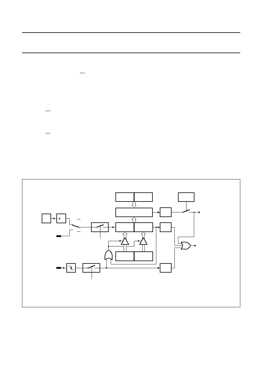
2001 Jun 19
40
Philips Semiconductors
Product specification
80C51 Ultra Low Power (ULP) telephony controller
P83CL882
6.6.4
A
UTO
-
RELOAD MODE
In the Auto-reload mode, Timer 2 can be configured as
a timer or a counter (T2CON.C/T2 bit) and then
programmed to count up or down. The counting direction
is determined by bit T2MOD.DCEN (down count enable).
When reset is applied, then T2MOD.DCEN is reset which
defaults to counting up. If T2MOD.DCEN is set, Timer 2
can count up when T2EX = 1 and count down when
T2EX = 0.
∑
T2CON.C/T2 = 1: Timer 2 is a 16-bit counter. The
counter increments/decrements at each LOW-to-HIGH
transition on input T2 at a maximum rate of one each
12 f
psc
cycles.
∑
T2CON.C/T2 = 0: Timer 2 is a 16-bit timer. The timer
increments/decrements each 6 f
psc
cycles.
6.6.4.1
T2MOD.DCEN = 0: counting up
In the Auto-reload mode and counting up, registers
T2RCH/T2RCL are used to hold a reload value for
T2H/T2L.
By setting bit T2CON.EXEN2 the external trigger input
T2EX is enabled. When resetting bit T2CON.EXEN2, the
external trigger input T2EX is disabled.
∑
T2CON.EXEN2 = 1: The external trigger input T2EX is
enabled. Timer 2 is a 16-bit timer or counter.
A HIGH-to-LOW transition at input T2EX causes the
value in T2RCH/T2RCL to be reloaded in the Timer 2
T2H/T2L registers, and bit T2CON.EXF2 becomes set.
Also overflowing of Timer 2 causes the value in
T2RCH/T2RCL to be reloaded in the T2H/T2L registers
and sets bit T2CON.TF2.
∑
T2CON.EXEN2 = 0: The external trigger input T2EX is
disabled. Timer 2 is a 16-bit timer or counter. The T2EX
input is ignored. Overflowing of Timer 2 causes the
value in T2RCH/T2RCL to be reloaded in the T2H/T2L
registers and sets bit T2CON.TF2.
Timer 2 interrupt will be set if EXF2 is set or TF2 is set.
The Auto-reload mode (DCEN = 0) is shown in Fig.20.
handbook, full pagewidth
MBH999
TL2
(8 BITS)
COMPARATOR 1
(16 BITS)
TR2
control
TH2
(8 BITS)
COMP2L
COMP2H
ECOMP
RCAP2L
RCAP2H
EXF2
TF2
COMP
Timer 2
interrupt
port
P1.2
EXEN2
control
C/T2 = 1
T2 pin
6
OSC
transition
detector
T2EX pin
C/T2 = 0
reload
Fig.20 Timer 2 in Auto-reload mode (DCEN = 0).
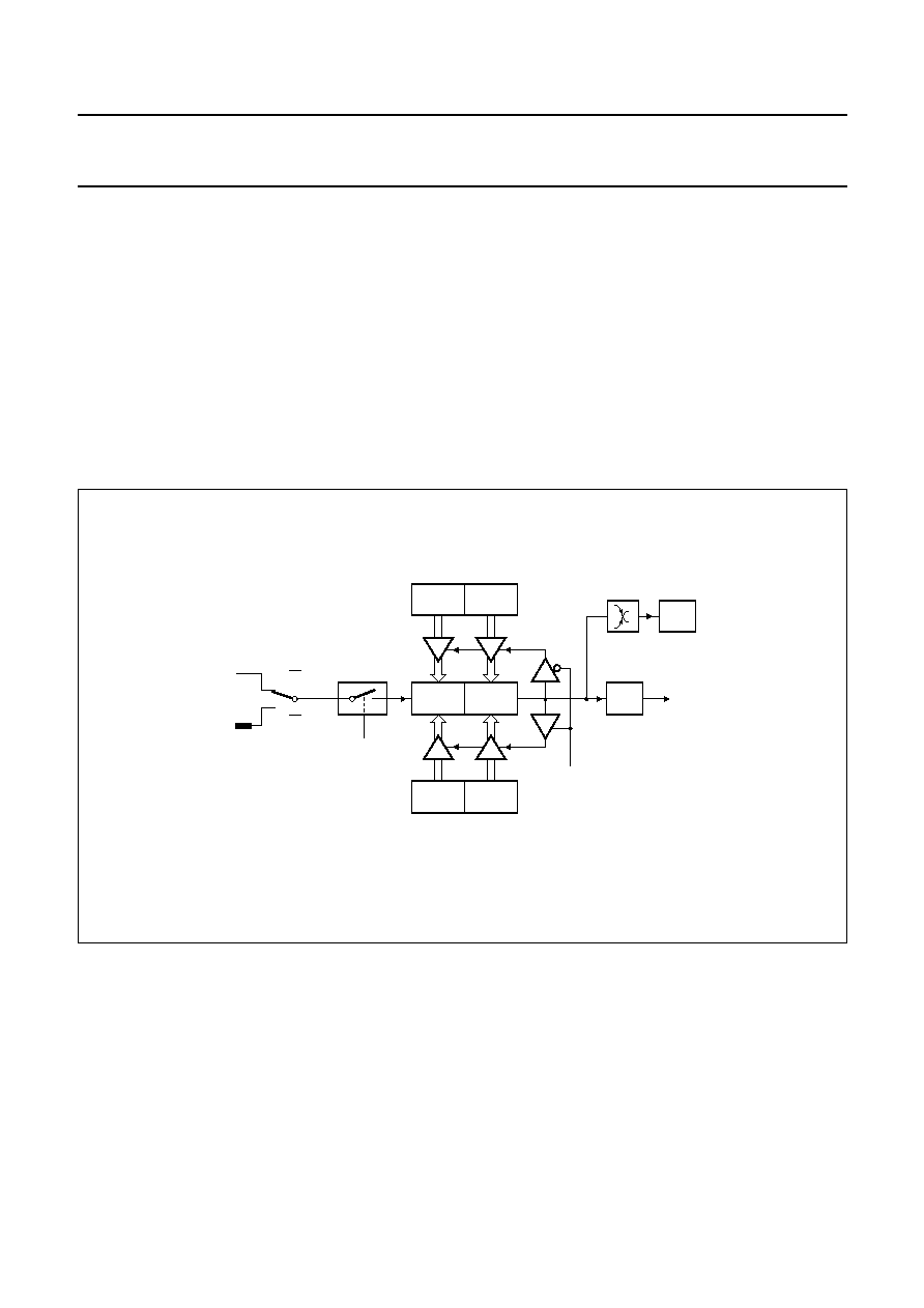
2001 Jun 19
41
Philips Semiconductors
Product specification
80C51 Ultra Low Power (ULP) telephony controller
P83CL882
6.6.4.2
T2MOD.DCEN = 1: T2EX = 1: counting up
The HIGH value of the external trigger input T2EX sets
Timer 2 to a count-up mode. In the Auto-reload mode and
counting up, registers T2RCH/T2RCL are used to hold
a reload value for T2H/T2L. Overflowing of Timer 2 causes
the value in T2RCH/T2RCL to be reloaded in the T2H/T2L
registers, sets bit T2CON.TF2 and toggles bit
T2CON.EXF2 (T2CON.EXF2 can be used as 17th bit if
desired). Timer 2 interrupt will be set if TF2 is set.
6.6.4.3
T2MOD.DCEN = 1: T2EX = 0: counting down
The LOW value of the external trigger input T2EX sets
Timer 2 to a count down mode.
In the Auto-reload mode and counting down, registers
T2RCH/T2RCL are used to hold a value for detecting an
underflow of T2H/T2L. Underflow occurs if the contents of
T2H/T2L matches the contents of T2RCH/T2RCL. Upon
underflow, bit TF2 will be set and registers T2H/T2L will be
loaded with FFFFH, bit T2CON.TF2 is set and bit
T2CON.EXF2 toggles (T2CON.EXF2 can be used as
17th bit if desired).
Note that a Timer 2 roll over from 0000H to FFFFH is not
considered as an underflow (only when
T2RCH/T2RCL = 0000H). Timer 2 interrupt will be set if
TF2 is set.
The Auto-reload mode (DCEN = 1) is shown in Fig.21.
MGT296
T2L
TR2
control
T2H
TF2
down count reload value
upcount reload value
T2RCL
T2RCH
FFH
FFH
EXF2
toggle
T2EX: 1 = count up
0 = count down
Timer 2
interrupt
C/ T2 = 1
T2
fpsc
C/ T2 = 0
Fig.21 Timer 2 in Auto-reload mode (DCEN = 1).
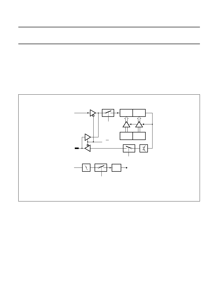
2001 Jun 19
42
Philips Semiconductors
Product specification
80C51 Ultra Low Power (ULP) telephony controller
P83CL882
6.6.5
C
LOCK OUTPUT MODE
In the Clock output mode, the output T2OUT is enabled as
a clock output. A timer overflow will cause T2H/T2L to be
loaded with T2RCH/T2RCL and will toggle output T2OUT.
The frequency of pin T2OUT is half the overflow
frequency.
Bit T2CON.EXF2 will be set if T2CON.EXEN2 is set and
a HIGH-to-LOW transition is detected on the T2EX pin.
Timer 2 interrupt will be set only if T2CON.EXF2 is set.
This makes an extra external interrupt available.
If Timer 2 does not operate in the Clock output mode, the
output T2OUT remains as specified by the I/O SFRs.
The Clock output mode is shown in Fig.22.
MGT297
T2L
TR2
T2H
T2RCL
T2RCH
EXF2
T2EX
toggle
Timer 2
interrupt
T2OUT
fpsc
EXEN2
T2OE
C/ T2
Fig.22 Timer 2 in Clock output mode.

2001 Jun 19
43
Philips Semiconductors
Product specification
80C51 Ultra Low Power (ULP) telephony controller
P83CL882
6.7
Watchdog Timer
The Watchdog Timer consists of an 8-bit down counter
and a Watchdog prescaler. The binary number defined by
bits WD3 to WD0 (WDCON SFR), the Watchdog prescaler
and the timer prescaler (f
psc
) defines the expiration time of
the Watchdog Timer. Once enabled this counter runs
continuously. Once expired the timer produces firstly an
interrupt and finally a reset. The software must reload the
Watchdog Timer at regular intervals to avoid expiration.
A positive edge on bit LD (WDCON SFR) (re)loads the
counter with the value of WD3 to WD0, sets the LOW bits
to logic 1 and activates this counter if it is not yet running.
However, to prepare the (re)loading a positive edge must
be applied to the COND bit in WDCON.
In this way at least two locations in software are needed
before the counter can be reloaded.
After reset the counter is not running. Only after the first
load (LD) it is clocked continuously by a clock pulse.
If the next LD signal is not given within the defined
expiration interval an overflow occurs and the processor
will be reset (signal WDR). One clock cycle (seen from the
Watchdog prescaler output) before the reset is applied a
WDI interrupt is issued. This gives the opportunity to avoid
the reset if required. The maximum Watchdog Timer
expiration time is thus 254/f
psc
to the WD interrupt and
255/f
psc
to the reset.
6.7.1
W
ATCHDOG
T
IMER
C
ONTROL
R
EGISTER
(WDCON)
The WDCON SFR is used to control the operation of the on-chip Watchdog Timer. If the Watchdog Timer is not loaded
after reset, the clock to the Watchdog Timer is switched off for power saving.
Table 53 Watchdog Timer Control Register (SFR address A5H; reset value = 0000 0000)
Table 54 Description of WDCON bits
7
6
5
4
3
2
1
0
COND
WD3
WD2
WD1
WD0
MSKPOL
-
LD
BIT
SYMBOL
DESCRIPTION
7
COND
load condition; control signal from processor
6
WD3
WD0 to WD3 is the preset value for the high nibble of the Watchdog Timer
5
WD2
4
WD1
3
WD0
2
MSKPOL
this bit controls the polarity of the input signal to the MSK modem;
MSKPOL = 0: input directly connected to the MSK modem
MSKPOL = 1: input inverted and connected to the MSK modem
1
-
reserved, must be kept to logic 0
0
LD
load Watchdog Timer with WD0 to WD3; control signal from CPU
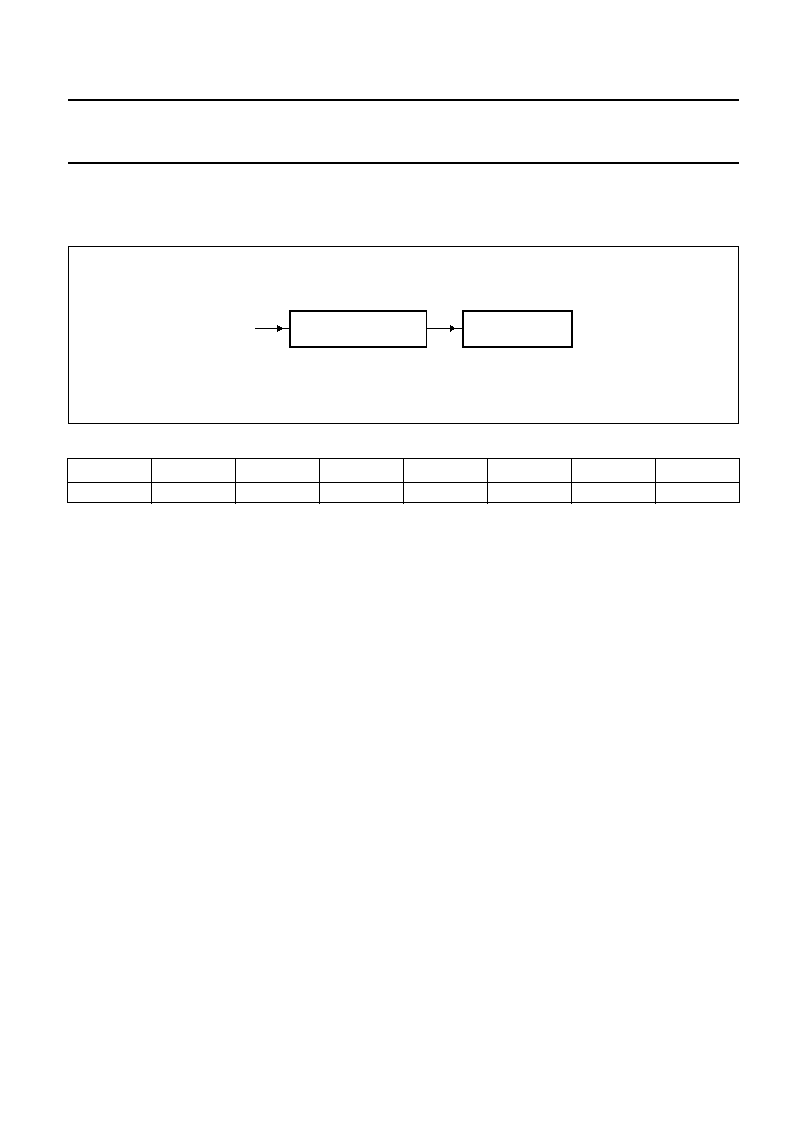
2001 Jun 19
44
Philips Semiconductors
Product specification
80C51 Ultra Low Power (ULP) telephony controller
P83CL882
6.7.2
W
ATCHDOG
T
IMER
P
RESCALER
R
EGISTER
(WDTIM)
The WDTIM SFR is used to initialize the prescaler of the on-chip Watchdog Timer.
Table 55 Watchdog Timer Prescaler Register (SFR address A6H; reset value 0000 0000)
The expiration time (t
exp)
can be calculated as follows:
Where:
prescaler factor = the dividing factor from prescaler (PSC1 and PSC2); 1, 2, 4, 6, 8, 10, 12 and 16
WDTIM = the 8-bit value (0 to 255) in the Watchdog Timer Prescaler Register
WDCON = the 4-bit value (0 to 15) reloaded in the Watchdog Timer
clock period = the period of the signal applied to pin XTAL1.
From the t
exp
formulae it follows that the maximum expiration time is:
t
exp(max)
= 16
◊
(2 + 64
◊
256)
◊
16
◊
(16)
◊
(clock period) = 67 206 016
◊
(clock period)
and the minimum expiration time is:
t
exp(min)
= 1
◊
66
◊
16
◊
(clock period) = 1056
◊
(clock period)
6.7.3
E
XAMPLE SEQUENCE TO RELOAD THE
W
ATCHDOG
T
IMER
An example of the reload sequence for the Watchdog Timer:
MOV WDCON,#00H;Clear COND and LD bit
ORL WDCON,#80H;Positive edge WDCON.7, prepare condition
ORL WDCON,#01H;Positive edge WDCON.0, reload the timer
7
6
5
4
3
2
1
0
WDTIM.7
WDTIM.6
WDTIM.5
WDTIM.4
WDTIM.3
WDTIM.2
WDTIM.1
WDTIM.0
MGT298
WATCHDOG TIMER
WATCHDOG PRESCALER
(WDTIM)
fpsc
Fig.23 Clocking the Watchdog timer.
t
exp
prescaler factor
(
)
2
64
WDTIM
1
+
(
)
◊
+
{
}
◊
16
WDCON
1
+
(
)
◊
◊
clock period
(
)
◊
=

2001 Jun 19
45
Philips Semiconductors
Product specification
80C51 Ultra Low Power (ULP) telephony controller
P83CL882
6.8
I
2
C-bus serial I/O (master/slave interface)
The I
2
C-bus implements a master/slave I
2
C-bus interface
with integrated shift register, shift timing generation and
slave address recognition. I
2
C-bus standard mode
(100 kHz SCLK) and fast mode (400 kHz SCLK) are
supported. Low speed mode and extended 10-bit
addressing are not supported.
The I
2
C-bus consists of two lines: a data line (SDA) and
a clock line (SCL). These lines also function as the I/O port
lines P1.7 and P1.6 respectively. The system is unique
because data transport, clock generation, address
recognition and bus control arbitration are all controlled by
hardware.
The I
2
C-bus serial I/O has complete autonomy in byte
handling and operates in 4 modes:
∑
Master transmitter
∑
Master receiver
∑
Slave transmitter
∑
Slave receiver.
These functions are controlled by the S1CON register.
S1STA is the Serial Status Register whose contents may
also be used as a vector to various service routines.
S1DAT is the Data Shift Register and S1ADR the Slave
Address Register. Slave address recognition is performed
by on-chip hardware. The block diagram of the I
2
C-bus
serial I/O is shown in Fig.24.
The interface between the CPU and the I
2
C-bus logic,
referred to as `SIO1', is accomplished with four Special
Function Registers (see Table 56):
The I
2
C-bus interface is compliant to the specification as
described in
"The I
2
C-bus and how to use it" (ordering
number 9398 393 40011). This document includes also
a detailed description of the I
2
C-bus protocol.
Table 56 I
2
C-bus related SFRs
SFR
DESCRIPTION
SFR ADDRESS
RESET VALUE
S1CON
Serial Control Register
D8H
0000 0000
S1DAT
Data Shift Register
DAH
0000 0000
S1ADR
Address Register
DBH
0000 0000
S1STA
Serial Status Register
D9H
1111 1000

2001 Jun 19
46
Philips Semiconductors
Product specification
80C51 Ultra Low Power (ULP) telephony controller
P83CL882
6.8.1
S
ERIAL
C
ONTROL
R
EGISTER
(S1CON)
The CPU can read from and write to this 8-bit SFR. Two bits are affected by the SIO1 hardware: the SI bit is set when a
serial interrupt is requested, and the STO bit is cleared when a STOP condition is present on the I
2
C-bus. The STO bit
is also cleared when ENS1 = 0. Reset initializes S1CON to 00H.
Table 57 Serial Control Register (SFR address D8H)
Table 58 Description of S1CON bits
7
6
5
4
3
2
1
0
CR2
ENS1
STA
STO
SI
AA
CR1
CR0
BIT
SYMBOL
DESCRIPTION
7
CR2
This bit along with bits CR1 and CR0 determines the serial clock frequency when SIO is
in the Master mode; see Table 59. When CR2 = 0 the I
2
C-bus is in fast mode.
6
ENS1
ENABLE serial I/O. When ENS1 = 0, the serial I/O is disabled. SDA and SCL outputs
are in the high-impedance state; P1.6 and P1.7 function as open-drain ports. When
ENS1 = 1, the serial I/O is enabled. Output port latches P1.6 and P1.7 must be set to
logic 1; note 1.
5
STA
START flag. When this bit is set in Slave mode, the SIO hardware checks the status of
the I
2
C-bus and generates a START condition if the bus is free or after the bus becomes
free. If STA is set while the SIO is in Master mode, SIO will generate a repeated START
condition. ENS1 should not be used to temporarily release SIO1 from the I
2
C-bus since,
when ENS1 is reset, the I
2
C-bus status is lost. The AA flag should be used instead.
4
STO
STOP flag. When the STO bit is set while SIO1 is in a Master mode, a STOP condition
is transmitted to the I
2
C-bus. When the STOP condition is detected on the bus, the SIO1
hardware clears the STO flag. In a Slave mode, the STO flag may be set to recover from
an error condition. In this case, no STOP condition is transmitted to the I
2
C-bus.
However, the SIO1 hardware behaves as if a STOP condition has been received and
switches to the defined `not addressed' Slave receiver mode. The STO flag is
automatically cleared by the hardware.
If the STA and STO bits are both set, the STOP condition is transmitted to the I
2
C-bus if
SIO1 is in a Master mode (in a Slave mode, SIO1 generates an internal STOP condition
which is not transmitted). SIO1 then transmits a START condition. When the STO bit is
reset, no STOP condition will be generated.
3
SI
SIO interrupt flag. This flag is set, and an interrupt is generated, after any of the
following events occur:
∑
A start condition is generated in Master mode
∑
Own slave address has been received during AA = 1
∑
The general call address has been received while S1ADR0 = 1 and AA = 1
∑
A data byte has been received or transmitted in Master mode (even if arbitration is lost)
∑
A data byte has been received or transmitted as selected slave
∑
A STOP or START condition is received as selected slave receiver or transmitter.
If this flag is set, the I
2
C-bus is halted (by pulling down SCL). Received data is only valid
until this flag is reset.
2001 Jun 19
47
Philips Semiconductors
Product specification
80C51 Ultra Low Power (ULP) telephony controller
P83CL882
Note
1. If the serial I/O is not enabled (ENS1), the clock to the serial I/O is switched off for power saving.
Table 59 Selection of the serial clock frequency in the Master mode of operation
Bit rates greater than 400 kHz are outside the specified frequency range.
2
AA
Assert acknowledge. When this bit is set, an acknowledge (LOW level to SDA) is
returned during the acknowledge clock pulse on the SCL line when:
∑
Own slave address is received
∑
General call address is received (S1ADR.0 = 1)
∑
A data byte is received while the device is programmed to be a master receiver
∑
A data byte is received while the device is a selected slave receiver.
When SIO1 is in the addressed Slave transmitter mode, state C8H will be entered after
the last serial bit is transmitted. When SI is cleared, SIO1 leaves state C8H, enters the
not addressed Slave receiver mode, and the SDA line remains at a HIGH level. In state
C8H, the AA flag can be set again for future address recognition.
When SIO1 is in the not addressed Slave mode, its own slave address and the general
call address are ignored. Consequently, no acknowledge is returned, and a serial
interrupt is not requested. Thus, SIO1 can be temporarily released from the I
2
C-bus
while the bus status is monitored. While SIO1 is released from the bus, START and
STOP conditions are detected, and serial data is shifted in. Address recognition can be
resumed at any time by setting the AA flag. If the AA flag is set when the parts own
slave address or the general call address has been partly received, the address will be
recognized at the end of the byte transmission.
When this bit is reset, no acknowledge is returned. Consequently, no interrupt is
requested when the own slave address or general call address is received.
1
CR1
These two bits along with the CR2 bit determine the serial clock frequency when SIO is
in the Master mode; see Table 59.
0
CR0
CR2
CR1
CR0
f
per
DIVISOR
BIT RATE (kHz) AT f
per
3.58 MHz
4 MHz
6 MHz
0
0
0
10
358
400
(600)
0
0
1
20
179
200
300
0
1
0
30
119.33
133
199.5
0
1
1
40
89.5
100
150
1
0
0
80
44.75
50
75
1
0
1
120
29.83
33
49.5
1
1
0
160
22.38
25
37.5
1
1
1
not valid selection
-
-
-
BIT
SYMBOL
DESCRIPTION

2001 Jun 19
48
Philips Semiconductors
Product specification
80C51 Ultra Low Power (ULP) telephony controller
P83CL882
6.8.2
D
ATA
S
HIFT
R
EGISTER
(S1DAT)
S1DAT contains a byte of serial data to be transmitted or
a byte which has just been received. The CPU can read
from and write to this 8-bit SFR while it is not in the process
of shifting a byte. This occurs when SIO1 is in a defined
state and the serial interrupt flag is set. Data in S1DAT
remains stable as long as SI is set.
Data in S1DAT is always shifted from right to left: the first
bit to be transmitted is the MSB (bit 7) and after a byte has
been received, the first bit of received data is located at the
MSB of S1DAT. While data is being shifted out, data on the
bus is simultaneously being shifted in; S1DAT always
contains the last data byte present on the bus.
Thus, in the event of lost arbitration, the transition from
master transmitter to slave receiver is made with the
correct data in S1DAT. Reset initializes S1DAT to 00H.
S1DAT and the ACK flag form a 9-bit shift register which
shifts in or shifts out an 8-bit byte, followed by an
acknowledge bit.
The ACK flag is controlled by the SIO1 hardware and
cannot be accessed by the CPU. Serial data is shifted
through the ACK flag into S1DAT on the rising edges of
clock pulses on the SCL line.
When a byte has been shifted into S1DAT, the serial data
is available in S1DAT, and the acknowledge bit is returned
by the control logic during the ninth clock pulse. Serial data
is shifted out from S1DAT via a buffer on the falling edges
of clock pulses on the SCL line.
When the CPU writes to S1DAT, the buffer is loaded with
the contents of S1DAT.7 which is the first bit to be
transmitted to the SDA line. After nine serial clock pulses,
the eight bits in S1DAT will have been transmitted to the
SDA line, and the acknowledge bit will be present in ACK.
Note that the eight transmitted bits are shifted back into
S1DAT.
Table 60 Data Shift Register (SFR address DAH)
Table 61 Description of S1DAT bits
7
6
5
4
3
2
1
0
S1DAT.7
S1DAT.6
S1DAT.5
S1DAT.4
S1DAT.3
S1DAT.2
S1DAT.1
S1DAT.0
BIT
SYMBOL
DESCRIPTION
7 to 1
S1DAT.[7:0]
Eight data bits, to be transmitted or just received. A logic 1 in S1DAT corresponds to a
HIGH level on the I
2
C-bus, and a logic 0 corresponds to a LOW level on the bus. Serial
data transmission of S1DAT is MSB first.
2001 Jun 19
49
Philips Semiconductors
Product specification
80C51 Ultra Low Power (ULP) telephony controller
P83CL882
6.8.3
A
DDRESS
R
EGISTER
(S1ADR)
The CPU can read from and write to this 8-bit SFR. S1ADR is not affected by the SIO1 hardware. The contents of this
register are irrelevant when SIO1 is in a Master mode.
In the Slave modes, the seven most significant bits must be loaded with the microcontrollers own slave address, and, if
the least significant bit is set, the general call address (00H) is recognized; otherwise it is ignored. Reset initializes
S1ADR to 00H.
Table 62 Address Register (SFR address DBH)
Table 63 Description of S1ADR bits
6.8.4
S
ERIAL
S
TATUS
R
EGISTER
(S1STA)
S1STA is an 8-bit read-only Special Function Register. The three least significant bits are always zero. The five most
significant bits contain the status code. There are 26 possible status codes. When S1STA contains F8H, no relevant
state information is available and no serial interrupt is requested. Reset initializes S1STA to F8H. All other S1STA values
correspond to defined SIO1 states. When each of these states is entered, a serial interrupt is requested (SI = 1).
The status codes for all possible modes of the I
2
C-bus interface are given in Table 66.
The contents of this register may be used as a vector to a service routine. This optimizes the response time of the
software and consequently that of the I
2
C-bus. S1STA is a read-only register.
Table 64 Serial Status Register (SFR address D9H)
Table 65 Description of S1STA bits
7
6
5
4
3
2
1
0
SLA6
SLA5
SLA4
SLA3
SLA2
SLA1
SLA0
GC
BIT
SYMBOL
DESCRIPTION
7 to 1
SLA[6:0]
These bits correspond to the 7-bit slave address which will be recognized on the
incoming data stream from the I
2
C-bus; when the slave address is detected and the
interface is enabled, a serial interrupt will be generated to the CPU.
0
GC
This bit is used to determine whether the general CALL address is recognized. When a
logic 0, the general CALL address is not recognized; when a logic 1, the general CALL
address is recognized.
7
6
5
4
3
2
1
0
SC4
SC3
SC2
SC1
SC0
0
0
0
BIT
SYMBOL
DESCRIPTION
3 to 7
SC[4:0]
5-bit status code
0 to 2
-
these three bits are held LOW

2001 Jun 19
50
Philips Semiconductors
Product specification
80C51 Ultra Low Power (ULP) telephony controller
P83CL882
Table 66 Status codes for the different modes
S1STA
VALUE
DESCRIPTION
MST/TRX mode
08H
a START condition has been transmitted
10H
a repeated START condition has been transmitted
18H
SLA and W have been transmitted, ACK has been received
20H
SLA and W have been transmitted, ACK received
28H
DATA of S1DAT has been transmitted, ACK received
30H
DATA of S1DAT has been transmitted, ACK received
38H
arbitration lost in SLA, R/W or DATA
MST/REC mode
38H
arbitration lost while returning ACK
40H
SLA and R have been transmitted, ACK received
48H
SLA and R have been transmitted, ACK received
50H
DATA has been received, ACK returned
58H
DATA has been received, ACK returned
SLV/REC mode
60H
own SLA and W have been received, ACK returned
68H
arbitration lost in SLA, R/W as MST; own SLA and W have been received, ACK returned
70H
general CALL has been received, ACK returned
78H
arbitration lost in SLA, R/W as MST; general CALL has been received
80H
previously addressed with own SLA; DATA byte received, ACK returned
88H
previously addressed with own SLA; DATA byte received, ACK returned
90H
previously addressed with general CALL; DATA byte has been received, ACK has been returned
98H
previously addressed with general CALL; DATA byte has been received, ACK has been returned
A0H
a STOP condition or repeated START condition has been received while still addressed as SLV/REC or
SLV/TRX
SLV/TRX mode
A8H
own SLA and R have been received, ACK returned
B0H
arbitration lost in SLA, R/W as MST. Own SLA and R have been received, ACK returned
B8H
DATA byte has been transmitted, ACK received
C0H
DATA byte has been transmitted, ACK received
C8H
last DATA byte has been transmitted (AA = 0), ACK received
Miscellaneous
00H
bus error during MST mode or selected SLV mode, due to an erroneous START or STOP condition
F8H
no information available (reset value). The serial interrupt flag SI, is not yet set

2001 Jun 19
51
Philips Semiconductors
Product specification
80C51 Ultra Low Power (ULP) telephony controller
P83CL882
Table 67 Symbols used in Table 66
SYMBOL
DESCRIPTION
SLA
7-bit slave address
R
Read bit
W
Write bit
ACK
acknowledgement (acknowledge bit = logic 0)
ACK
no acknowledgement (acknowledge bit = logic 1)
DATA
8-bit data byte to or from I
2
C-bus
MST
master
SLV
slave
TRX
transmitter
REC
receiver
6.8.5
M
ODES OF OPERATION
The I
2
C-bus logic may operate in any of the following four
modes:
∑
Master transmitter
∑
Master receiver
∑
Slave transmitter
∑
Slave receiver.
As a master, the I
2
C-bus logic will generate all of the serial
clock pulses and the START and STOP conditions.
A transfer is ended with a STOP condition or with
a repeated START condition. Since a repeated START
condition is also the beginning of the next serial transfer,
the I
2
C-bus will not be released.
Two types of data transfers are possible on the I
2
C-bus:
∑
Data transfer from a master transmitter to a slave
receiver. The first byte transmitted by the master is the
slave address. Next follows a number of data bytes. The
slave returns an acknowledge bit after each received
byte.
∑
Data transfer from a slave transmitter to a master
receiver. The first byte (the slave address) is transmitted
by the master. The slave then returns an acknowledge
bit. Next follows the data bytes transmitted by the slave
to the master. The master returns an acknowledge bit
after each received byte except the last byte. At the end
of the last received byte, a `not acknowledge' is
returned.
In a given application, SIO1 may operate as a master and
as a slave. In the Slave mode, the SIO1 hardware looks for
its own slave address and the general call address. If one
of these addresses is detected, an interrupt is requested.
When the microcontroller wishes to become the bus
master, the hardware waits until the bus is free before the
Master mode is entered so that a possible slave action is
not interrupted. If bus arbitration is lost in the Master mode,
SIO1 switches to the Slave mode immediately and can
detect its own slave address in the same serial transfer.
6.8.5.1
Master transmitter mode
Serial data is output through SDA while SCL outputs the
serial clock. The first byte transmitted contains the slave
address (7-bit SLA) of the receiving device and the data
direction bit. In this case the data direction bit (R/W) will be
a logic 0 (W). Serial data is transmitted 8 bits at a time.
After each byte is transmitted, an acknowledge bit is
received. START and STOP conditions are output to
indicate the beginning and the end of a serial transfer.
In the Master transmitter mode, a number of data bytes
can be transmitted to the slave receiver. Before the Master
transmitter mode can be entered, S1CON must be
initialized with the ENS1 bit set and the STA, STO and
SI bits reset. ENS1 must be set to enable the SIO1
interface. If the AA bit is reset, SIO1 will not acknowledge
its own slave address or the general call address if they
are present on the bus. This will prevent the SIO1 interface
from entering a Slave mode.

2001 Jun 19
52
Philips Semiconductors
Product specification
80C51 Ultra Low Power (ULP) telephony controller
P83CL882
The Master transmitter mode may now be entered by
setting the STA bit. The SIO1 logic will then test the
I
2
C-bus and generate a start condition as soon as the bus
becomes free. When a START condition is transmitted,
the serial interrupt flag (SI) is set, and the status code in
the Status Register (S1STA) will be 08H.
This status code must be used to vector to an interrupt
service routine that loads S1DAT with the slave address
and the data direction bit (SLA + W). The SI bit in S1CON
must then be reset before the serial transfer can continue.
When the slave address and the direction bit have been
transmitted and an acknowledgment bit has been
received, the serial interrupt flag (SI) is set again, and
a number of status codes in S1STA are possible.
The appropriate action to be taken for any of the status
codes is detailed in the table. After a repeated start
condition (state 10H), SIO1 may switch to the Master
receiver mode by loading S1DAT with SLA + R.
6.8.5.2
Master receiver mode
The first byte transmitted contains the slave address of the
transmitting device (7-bit SLA) and the data direction bit. In
this case the data direction bit (R/W) will be logic 1 (R).
Serial data is received via SDA while SCL outputs the
serial clock. Serial data is received 8 bits at a time. After
each byte is received, an acknowledge bit is transmitted.
START and STOP conditions are output to indicate the
beginning and end of a serial transfer.
In the Master receiver mode, a number of data bytes are
received from a slave transmitter. The transfer is initialized
as in the Master transmitter mode. When the START
condition has been transmitted, the interrupt service
routine must load S1DAT with the 7-bit slave address and
the data direction bit (SLA + R). The SI bit in S1CON must
then be cleared before the serial transfer can continue.
When the slave address and the data direction bit have
been transmitted and an acknowledgment bit has been
received, the serial interrupt flag (SI) is set again, and
a number of status codes are possible in S1STA.
The appropriate action to be taken for each of the status
codes is detailed in the table.
After a repeated start condition (state 10H), SIO1 may
switch to the Master transmitter mode by loading S1DAT
with SLA + W.
6.8.5.3
Slave receiver mode
Serial data and the serial clock are received through SDA
and SCL. After each byte is received, an acknowledge bit
is transmitted. START and STOP conditions are
recognized as the beginning and end of a serial transfer.
Address recognition is performed by hardware after
reception of the slave address and direction bit.
In the slave receiver mode, a number of data bytes are
received from a master transmitter. To initiate the Slave
receiver mode, S1ADR must be loaded with the 7-bit slave
address to which SIO1 will respond when addressed by a
master. Also the least significant bit of S1ADR should be
set if the interface should respond to the general call
address (00H).The Serial Control Register (S1CON)
should be initialized with ENS1 and AA set and STA, STO,
and SI reset in order to enter the Slave receiver mode.
Setting the AA bit will enable the logic to acknowledge its
own slave address or the general call address and ENS1
will enable the interface.
When S1ADR and S1CON have been initialized, SIO1
waits until it is addressed by its own slave address
followed by the data direction bit which must be logic 0 (W)
for SIO1 to operate in the Slave receiver mode. After its
own slave address and the W bit have been received, the
serial interrupt flag (SI) is set and a valid status code can
be read from S1DAT. This status code should be used to
vector to an interrupt service routine, and the appropriate
action to be taken for each of the status codes is detailed
in Table 66. The Slave receiver mode may also be entered
if arbitration is lost while SIO1 is in the Master mode.
If the AA bit is reset during a transfer, SIO1 will return a not
acknowledge (logic 1) to SDA after the next received data
byte. While AA is reset, SIO1 does not respond to its own
slave address or a general call address. However, the
I
2
C-bus is still monitored and address recognition may be
resumed at any time by setting AA. This means that the
AA bit may be used to temporarily isolate SIO1 from the
I
2
C-bus.
6.8.5.4
Slave transmitter mode
The first byte is received and handled as in the Slave
receiver mode. However, in this mode, the direction bit will
indicate that the transfer direction is reversed. Serial data
is transmitted via SDA while the serial clock is input
through SCL. START and STOP conditions are
recognized as the beginning and end of a serial transfer.
In the Slave transmitter mode, a number of data bytes are
transmitted to a master receiver. Data transfer is initialized
as in the Slave receiver mode. When S1ADR and S1CON
have been initialized, SIO1 waits until it is addressed by its
own slave address followed by the data direction bit which
must be logic 1 (R) for SIO1 to operate in the Slave
transmitter mode.

2001 Jun 19
53
Philips Semiconductors
Product specification
80C51 Ultra Low Power (ULP) telephony controller
P83CL882
After its own slave address and the R bit have been
received, the serial interrupt flag (SI) is set and a valid
status code can be read from S1STA. This status code is
used to vector to an interrupt service routine, and the
appropriate action to be taken for each of these status
codes is detailed in the table. The Slave transmitter mode
may also be entered if arbitration is lost while SIO1 is in the
Master mode.
If the AA bit is reset during a transfer, SIO1 will transmit the
last byte of the transfer and enter state C0H or C8H. SIO1
is switched to the not addressed Slave mode and will
ignore the master receiver if it continues the transfer. Thus
the master receiver receives all logic 1s as serial data.
While AA is reset, SIO1 does not respond to its own slave
address or a general call address. However, the I
2
C-bus is
still monitored, and address recognition may be resumed
at any time by setting AA. This means that the AA bit may
be used to temporarily isolate SIO1 from the I
2
C-bus.
6.8.6
F
UNCTIONAL DESCRIPTION
I
2
C-
BUS INTERFACE
6.8.6.1
Input filter
Input signals SDA and SCL from I/O pad cells are
synchronized with f
per
, and spikes shorter than three clock
periods are filtered out.
6.8.6.2
Arbitration and control logic
In the Master transmitter mode, the arbitration logic checks
that every transmitted logic 1 actually appears as a logic 1
on the I
2
C-bus. If another device on the bus overrules
a logic 1 and pulls the SDA line LOW, arbitration is lost,
and SIO1 immediately changes from master transmitter to
slave receiver. SIO1 will continue to output clock pulses
(on SCL) until transmission of the current serial byte is
complete.
Arbitration may also be lost in the Master receiver mode.
Loss of arbitration in this mode can only occur while SIO1
is returning a `not acknowledge' (logic 1) to the bus.
Arbitration is lost when another device on the bus pulls this
signal LOW. Since this can occur only at the end of a serial
byte, SIO1 generates no further clock pulses.
The synchronization logic will synchronize the serial clock
generator with the clock pulses on the SCL line from
another device. If two or more master devices generate
clock pulses, the `mark' duration is determined by the
device that generates the shortest `marks,' and the `space'
duration is determined by the device that generates the
longest `spaces'.
A slave may stretch the space duration to slow down the
bus master. The space duration may also be stretched for
handshaking purposes. This can be done after each bit or
after a complete byte transfer. SIO1 will stretch the SCL
space duration after a byte has been transmitted or
received and the acknowledge bit has been transferred.
The serial interrupt flag (SI) is set, and the stretching
continues until the serial interrupt flag is cleared.
This block also controls all of the signals for serial byte
handling. It provides the shift pulses for S1DAT, enables
the comparator, generates and detects START and STOP
conditions, receives and transmits acknowledge bits,
controls the Master and Slave modes, contains interrupt
request logic and monitors the I
2
C-bus status.
6.8.6.3
Bus clock generator
This programmable clock pulse generator provides the
SCL clock pulses when SIO1 is in the Master transmitter
or Master receiver mode. It is switched off when SIO1 is in
a Slave mode. The output frequency is dependent on the
CR bits in the control register. The output clock pulses
have a 50% duty cycle unless the clock generator is
synchronized with other SCL clock sources as described
above.
6.8.6.4
Address Register (S1ADR) and comparator
This 8-bit SFR may be loaded with the 7-bit slave address
to which SIO1 will respond when programmed as a slave.
The least significant bit is used to enable the general call
address recognition.
The comparator compares the received 7-bit slave
address with its own slave address. It also compares the
first received byte with the general call address. If an
equality is found, the appropriate status bits are set and an
interrupt is requested.
6.8.6.5
Data Shift Register (S1DAT)
This 8-bit SFR contains a byte of serial data to be
transmitted or a byte which has just been received. Data in
S1DAT is always shifted from right to left; the first bit to be
transmitted is the MSB (bit 7) and, after a byte has been
received, the first bit of received data is located at the MSB
of S1DAT. While data is being shifted out, data on the bus
is simultaneously being shifted in; S1DAT always contains
the last byte present on the bus. Thus, in the event of lost
arbitration, the transition from master transmitter to slave
receiver is made with the correct data in S1DAT.

2001 Jun 19
54
Philips Semiconductors
Product specification
80C51 Ultra Low Power (ULP) telephony controller
P83CL882
6.8.6.6
Serial Control Register (S1CON)
This 8-bit SFR is used by the microcontroller to control the
generation of START and STOP conditions, enable the
interface, control the generation of ACKs, and to select the
clock frequency.
6.8.6.7
Serial Status Register (S1STA)
The status decoder takes all of the internal status bits and
compresses them into a 5-bit code. This code is unique for
each I
2
C-bus status. The 5-bit code may be used to
generate vector addresses for fast processing of the
various service routines.
Each service routine processes a particular bus status.
There are 26 possible bus states if all four modes of SIO1
are used. The 5-bit status code is latched into the five most
significant bits of the status register when the serial
interrupt flag is set (by hardware) and remains stable until
the interrupt flag is cleared by software. The three least
significant bits of the Serial Status Register are always
zero. If the status code is used as a vector to service
routines, then the routines are displaced by eight address
locations. Eight bytes of code should be sufficient for most
of the service routines.
handbook, full pagewidth
MBC749 - 1
SLAVE ADDRESS
S1ADR
GC
SHIFT REGISTER
S1DAT
SDA
ARBITRATION LOGIC
SCL
BUS CLOCK GENERATOR
S1STA
INTERNAL BUS
7
6
5
4
3
2
1
0
S1CON
7
6
5
4
3
2
1
0
Fig.24 Block diagram of I
2
C-bus serial I/O.

2001 Jun 19
55
Philips Semiconductors
Product specification
80C51 Ultra Low Power (ULP) telephony controller
P83CL882
6.9
MSK modem
The MSK modem is used for in-band signalling between
handset and base in analog cordless telephone systems
CT0, CT1 and CT1+. The MSK modems receiver and
transmitter can be enabled separately. Receive and
transmit interrupts can wake-up the microcontroller during
its power saving Idle mode. Baud rates are programmable.
Figure 25 shows the functional diagram of the MSK
modem.
The modem has the following features:
∑
Full-duplex operation via an 8-bit parallel interface
∑
The message is fully Manchester coded/decoded
∑
Automatic detection of 16-bit Manchester preamble
pattern
∑
The last received 4 bits of the preamble pattern are
software programmable
∑
Receiver full, transmitter empty indication bits
∑
Manchester coding and decoding for clock recovery and
early error detection
∑
Programmable input polarity (see WDCON SFR;
Section 6.7.1)
∑
Baud rate selection of
1
/
2976
f
per
,
2
/
2976
f
per
,
3
/
2976
f
per
and
4
/
2976
f
per
∑
Receiver and transmitter off states with no power
consumption.
MGU221
80C51 CORE
MSTAT
MCON
RECEIVER
TRANSMITTER
TIMER
MBUF
MSK MODEM
TELX MICROCONTROLLER
MREN
MPR
MTEN
MB1,2
MCLK
Py.y
(1)
Px.x
(1)
MRI MTI
IBD (7-0)
AN (7-0)
R0
MOUT0
R1
MOUT1
R2
MOUT2
RF
SLICER
RF
VOUT
mouthpiece
TX_MUTE
RX_MUTE
earpiece
MIN
Fig.25 MSK modem functional diagram.
(1) The signals RX_MUTE and TX_MUTE are handled by software. Any available output pin can be used.

2001 Jun 19
56
Philips Semiconductors
Product specification
80C51 Ultra Low Power (ULP) telephony controller
P83CL882
6.9.1
80C51
MICROCONTROLLER INTERFACE
The MSK modem block interfaces to the microcontroller via the interrupt signals MRI and MTI and via the control and
data SFRs MCON, MSTAT and MBUF. The MSK modem receive and transmit registers are both accessed via the
Special Function Register MBUF. Writing to MBUF loads the transmit register and reading MBUF accesses a physically
separate receive register.
Table 68 MSK modem related SFRs
6.9.1.1
MSK Modem Control Register (MCON)
Table 69 MSK Modem Control Register (SFR address D3H)
Table 70 Description of MCON bits
Note
1. If both the transmitter and the receiver are disabled (MTEN = 0 and MREN = 0), the clock of the MSK modem is
switched off. It is advised to use this state for power saving.
Table 71 Selection of the modems baud rates
SFR
DESCRIPTION
SFR ADDRESS
RESET VALUE
MCON
MSK Modem Control Register
D3H
0000 0000
MSTAT
MSK Modem Status Register
D2H
XX00 0000
MBUF
MSK Modem Data Buffer
D1H
0000 0000
7
6
5
4
3
2
1
0
MPR3
MPR2
MPR1
MPR0
MB1
MB0
MTEN
MREN
BIT
SYMBOL
DESCRIPTION
7
MPR3
Modem preamble pattern. These 4 bits define the modems preamble pattern.
6
MPR2
5
MPR1
4
MPR0
3
MB1
Modem transmit/receive frequency. These 2 bits define the modem transmit/receive
frequency; see Table 71.
2
MB0
1
MTEN
Modem Transmitter Enable. If this bit is set the transmitter is active and MOUT[2:0] will
get the value `100' if no data is transmitted. If reset, MOUT[2:0] will get the value `111' to
zero the currents in the resistive DAC; see note 1.
0
MREN
Modem Receiver Enable. If this bit is set the modem receiver is active and scans for
Manchester data; see note 1.
MB1
MB0
MODEM BAUD RATE
0
0
1
/
2976
f
per
0
1
2
/
2976
f
per
1
0
3
/
2976
f
per
1
1
4
/
2976
f
per

2001 Jun 19
57
Philips Semiconductors
Product specification
80C51 Ultra Low Power (ULP) telephony controller
P83CL882
6.9.1.2
MSK Modem Status Register (MSTAT)
Table 72 MSK Modem Status Register (SFR address D2H)
Table 73 Description of MSTAT bits
6.9.1.3
MSK Modem Data Buffer (MBUF)
Table 74 MSK Modem Data Buffer (SFR address D1H)
Table 75 Description of MBUF bits
7
6
5
4
3
2
1
0
-
-
MRF
MRE
MRP
MRL
MTI
MRI
BIT
SYMBOL
DESCRIPTION
5
MRF
Modem Receiver Full flag. MRF is set when MBUF holds a newly received byte. MRF
is reset if the receiver is disabled (MREN = 0) or by clearing MRI. This bit is read-only;
writing to it will have no effect.
4
MRE
Modem Receiver Error flag. Indicates the reception of a non-Manchester bit. This bit is
set by hardware and is reset by disabling the receiver (MREN = 0) or by clearing MRI.
This bit is read-only; writing to it will have no effect.
3
MRP
Modem Receiver Preamble flag. MRP is set by hardware when the modem recognizes
the programmed preamble pattern (AAAH) after locking the receiver clock (MRL = 1).
MRP is reset by hardware if the receiver is disabled (MREN = 0) or if non-Manchester
data is received (MRE = 1). This bit is read-only; writing to it will have no effect.
2
MRL
Modem Receiver Clock Locked flag. This bit is set when the clock of the receiver is
locked, i.e. when the receiver has detected three consecutive Manchester bits but has
not found the preamble pattern yet. MRL is reset when the receiver detects a
non-Manchester bit or when the receiver is disabled. This bit is read-only; writing to it
will have no effect.
1
MTI
Modem Transmit Interrupt flag. Indicates MBUF is empty and ready to accept a new
byte for transmission. MTI is reset by writing a logic 0 to it. Writing a logic 1 to MTI sets
the bit and allows a hardware interrupt to be generated by software.
0
MRI
Modem Receive Interrupt flag. Indicates:
Modem Receiver Full (MRF = 1) or
Modem Receiver Error (MRE = 1) or
Modem Receiver Preamble (MRP = 1) or
Modem Receiver Clock Locked (MRL = 1).
This bit is reset by writing a logic 0 to MRI. A reset of MRI will also reset MRE. Writing a
logic 1 to MRI will have no effect.
7
6
5
4
3
2
1
0
D7
D6
D5
D4
D3
D2
D1
D0
BIT
SYMBOL
DESCRIPTION
7 to 0
D7 to D0
Writing to MBUF loads the data into the transmit buffer and starts a transmission at
MOUT if the transmitter is enabled (MTEN = 1). A new byte can be loaded after MTI is
set. If a new byte is loaded before MTI is set the previous byte will be lost. After data has
been received at MIN, indicated by MRI, the received byte can be read from MBUF.

2001 Jun 19
58
Philips Semiconductors
Product specification
80C51 Ultra Low Power (ULP) telephony controller
P83CL882
6.9.2
M
ODEM INTERFACE
The modem block has the following modem interface
signals,
∑
MIN: MSK Manchester coded input signal from the data
slicer
∑
MOUT0 to MOUT2: 3-bit Manchester coded output
signal of the modem.
The MSK receiver input can be inverted by programming
bit MSKPOL (WDCON.2; see Section 6.7.1):
∑
MSKPOL = 0: direct connection between the MIN pin
and MSK receiver
∑
MSKPOL = 1: inverted connection between the MIN pin
and MSK receiver.
The mute signals RX_MUTE and TX_MUTE must be
handled by software according to the progress in the data
transfer. Any standard I/O port pin can be used for this
purpose.
6.9.3
S
YNCHRONISATION
When enabled the receiver samples MIN with a frequency
f
sample
= 8
◊
baud rate. The sampled values are shifted
into an 8-bit shift register. This register is regularly checked
to determine whether it contains samples that fulfil the
Manchester coding rule, i.e. whether there is
a LOW-to-HIGH or a HIGH-to-LOW transition in the middle
of the bitcell.
Figure 26a shows a regular, full synchronized bitcell.
Figure 26b shows a regular, not synchronized bitcell, this
phase shift will be corrected in the next received bitcell.
Figure 26c (data is faster than internal timebase)
and Fig.26d (data is slower than internal timebase)
represent a non-valid, not synchronized bitcell. In the next
received bitcell the data will be re-synchronized but the
current data bit does not fulfil the Manchester coding rule
and will be lost.
The receiver searches for three consecutive sets of
8 samples that fulfil the Manchester coding rule.
If these three sets have been found the clock is locked
(MRL = 1) and the receiver starts looking for the
Manchester preamble pattern.
From this point on the receiver uses a Phase-Locked
Loop (PLL) to adjust the synchronisation after each
received Manchester bit. To detect a sample shift the
receiver uses all 8 samples. If the data is at maximum, one
sample out of phase, the receiver is able to resynchronize
without losing data. If the data is up to three samples out
of phase the receiver can still resynchronize but the data
is lost. The correction is done by shifting only one sample
per bitcell. This means up to three bit cells are needed for
full resynchronisation. If the receiver is not able to
establish resynchronization within three bitcells the lock bit
(MRL) will be reset.
Therefore the MSK modem can receive correct input data
with maximum jitter of 1/f
sample
.
MGT299
MIN
1 2 3 4 5 6 7 8
(a)
1 2 3 4 5 6 7 8
(c)
1 2 3 4 5 6 7 8
(d)
1 2 3 4 5 6 7 8
(b)
MIN
MIN
MIN
Fig.26 Schematic representation of a bitcell.

2001 Jun 19
59
Philips Semiconductors
Product specification
80C51 Ultra Low Power (ULP) telephony controller
P83CL882
6.9.4
D
ATA RECEPTION
A message is received as a block of one or more data
bytes. When enabled, the receiver starts sampling MIN
and tries to detect a Manchester pattern. As soon as
3 consecutive Manchester bits are detected the receiver
clock is locked (MRL = 1) and the receiver starts scanning
the incoming data for the programmed Manchester
preamble pattern. When the modem recognizes the
preamble pattern, bit MRP is set to a logic 1.
If a non-Manchester bit is detected before finding the
preamble pattern then MRL is reset and MRE is set to
a logic 1. The synchronisation process has to restart. If the
preamble pattern has been detected the receiver starts to
Manchester decode the incoming data bits and shifts them
into an internal register. After 8 bits the contents of the
internal register are copied to MBUF and the MRF bit is set
to a logic 1. The received byte can be read from MBUF
while receiving continues in the internal register. If a
non-Manchester bit is received during data reception then
MRE is set to a logic 1 and MRL and MRP are reset. The
receiver has to resynchronize before receiving new data.
Whenever one of the bits MRF, MRE, MRP and MRL is set
the MRI bit is also set and a MSK receive interrupt is
generated. This means that when a MSK receive interrupt
occurs the 4 status bits have to be polled by software.
The bit MRL allows the software to decide very quickly
whether an occupied channel contains Manchester coded
data or not. The MRP bit is used to find the start of data
transmission in a message that is repeated over and over
again. MRE is used to detect a Manchester error, which is
a violation of the Manchester coding rule that the received
level should change in the middle of a bitcell. The MRF bit
indicates that the data in MBUF is ready to be read by the
software.
During data reception the minimum time between two
settings of MRF (each one generating an MRI interrupt) is:
Figure 27 shows an example of the data reception timing
diagram.
t
min
8
baud rate
-------------------------
=
MGU222
MIN
data
37
no Manchester
code: speech??
no Manchester
code: speech??
data
AA
data
AD
data
1F
data
37
80C51
access
MRI
MRL
MRP
MRE
MRF
write
MREN = 1
clear
RTI
clear
RTI
clear
RTI
read
MBUF
1F
read
MBUF
37
RX_MUTE should be generated
by microcontroller upon interrupt
RX_MUTE should be cleared by
microcontroller at end of message
Fig.27 Data reception timing diagram.
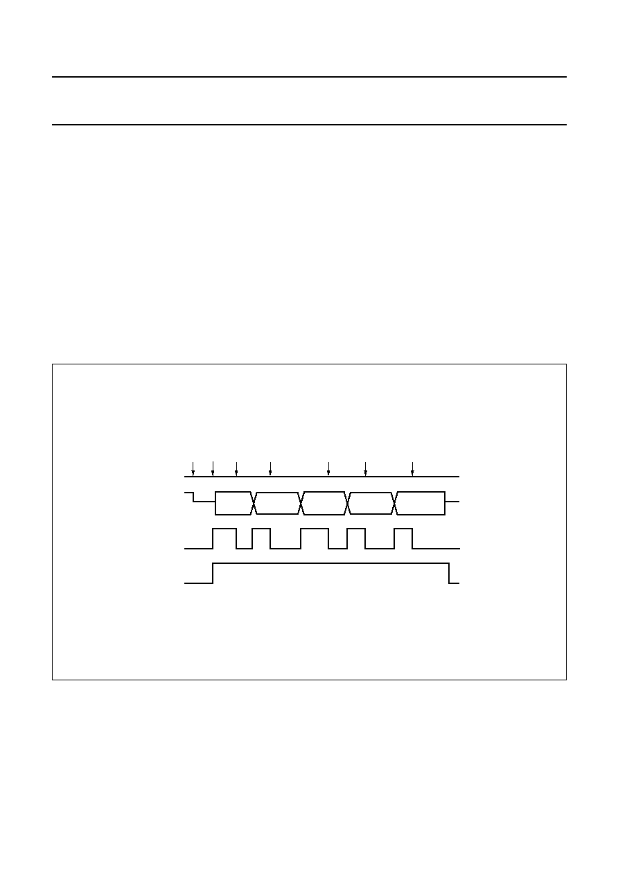
2001 Jun 19
60
Philips Semiconductors
Product specification
80C51 Ultra Low Power (ULP) telephony controller
P83CL882
6.9.5
D
ATA TRANSMISSION
Data transmission is enabled if bit MTEN in register MCON
is set to a logic 1. If MTEN is a logic 0, data transmission
is disabled and MOUT[2:0] is set to `111' to zero the
currents in the resistive DAC. Setting MTEN to a logic 1
sets MOUT[2:0] to the idle value `100'. This results in
a value close to
1
/
2
V
DD
on the output signal of the external
DAC. Transmission is started by loading the first byte into
register MBUF. All bytes are transmitted starting with the
MSB.
A message is transferred in a block of 3 or more bytes, the
first two bytes being the programmed Manchester
preamble pattern. In order to insert the preamble pattern,
the first two bytes AAH and AxH (with `x' being the
MPR3 to MPR0 value programmed in the receiver MSK
modem) have to be written to MBUF by software.
After this, the first byte of the message is written to MBUF.
As soon as MBUF is ready to accept new input, signal MTI
is set.
The minimum time between two MTI interrupts is:
If no new byte is written to MBUF at the end of a byte
transmission, the modem transmitter stops transmission
and MOUT[2:0] is set to the idle state `100'.
MTI must be cleared explicitly. If MTEN is reset during
transmission, the transmitter will finish the transmission of
the current byte and then will set MOUT[2:0] to the off
state `111'. No interrupt on MTI will be generated at the
end of the transmission.
t
min
8
baud rate
-------------------------
=
handbook, full pagewidth
MGK229
MOUT
80C51
access
set
MTEN
clear
MTI
write
MBUF
AAH
write
MBUF
ADH
write
MBUF
AAH
write
MBUF
55H
write
MBUF
55H
MTI
TX_MUTE
data ADH
data AAH
data AAH
data 55H
data 55H
Fig.28 Data transmission timing diagram.
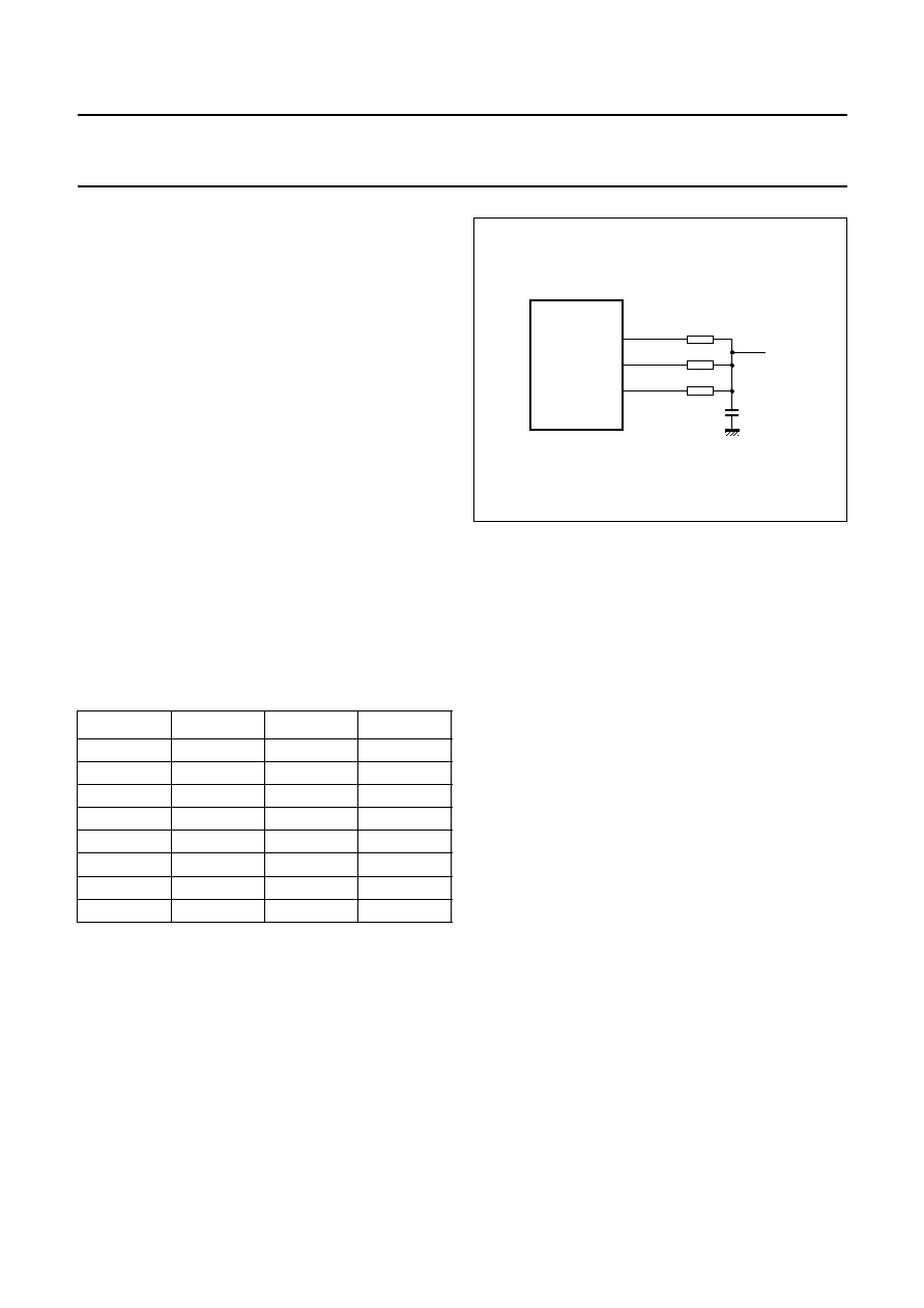
2001 Jun 19
61
Philips Semiconductors
Product specification
80C51 Ultra Low Power (ULP) telephony controller
P83CL882
6.9.6
W
AVEFORM GENERATION WITH
MOUT[2:0]
The 3 digital output pins MOUT0 to MOUT2, should be
used as an input to a 3-bit external DAC. The signals can
be connected via external resistors R0, R1 and R2 to
a summation point and then be filtered with an external
capacitor (C1). The 3-bit DAC is shown in Fig.29. Table 76
gives the relationship between the MOUT pins and VOUT.
Figure 30 shows the waveforms that are produced by the
waveform generator. The horizontal axis shows the
sample counter on which the waveform changes its value.
Each bit is built-up out of 2
◊
124 samples.
The vertical axis shows the values of MOUT[2:0], forming
the inputs of the resistive DAC. The first half of the
waveform is determined by the previous and the current
bit, whereas the second half of the waveform is determined
by the current and the next bit to be transmitted. The count
frequency of the sample counter depends on the
programmed baud rate.
If the transmitter is disabled with MTEN set to a logic 0,
MOUT[2:0] is `111' to save power in the resistive DAC.
If the transmitter is enabled and no data is transmitted,
MOUT[2:0] has an idle value of `100', which corresponds
to 0.57V
DD
.
Table 76 VOUT as a function of MOUT[2:0]
Note
1. VOUT with resistor values (see Fig.29): R1 = 0.5R0;
R2 = 0.25R0
6.9.7
M
ANCHESTER CODING OF DATA
The bits of the data byte written in MBUF are Manchester
encoded as shown in Fig.30. A logic 1 is coded as
a LOW-to-HIGH transition in the middle of a bitcell,
a logic 0 is coded as a HIGH-to-LOW transition.The
Manchester encoded signal contains redundancy for early
error detection in received bits. A non-matching
HIGH-to-LOW or LOW-to-HIGH pair indicates an error
condition.The Manchester encoded signal has a polarity
change in each bitcell.
MOUT2
MOUT1
MOUT0
VOUT
(1)
0
0
0
0
0
0
1
0.14V
DD
0
1
0
0.29V
DD
0
1
1
0.43V
DD
1
0
0
0.57V
DD
1
0
1
0.71V
DD
1
1
0
0.86V
DD
1
1
1
V
DD
handbook, halfpage
MGK231
WAVEFORM
GENERATOR
MOUT0
MOUT1
MOUT2
R0
R1
R2
VOUT
C1 = 10 nF
Fig.29 3-bit DAC with MOUT[2:0].

2001 Jun 19
62
Philips Semiconductors
Product specification
80C51 Ultra Low Power (ULP) telephony controller
P83CL882
handbook, full pagewidth
MGK232
111
11
24
41
84
100
124
113
24
41
84
100
124
113
11
110
101
011
000
001
010
100
000
111
11
24
41
84
100
124
113
23
48
81
124
110
101
011
000
001
010
100
001
23
48
81
111
11
24
41
84
100
124
113
124
110
101
011
000
001
010
100
110
24
41
84
100 113
11
111
43
76
101
124
124
110
101
011
000
001
010
100
100
24
41
84
100 113
11
111
43
76
101
124
124
110
101
011
000
001
010
100
011
23
48
81
111
43
76
101
124
124
110
101
011
000
001
010
100
010
23
48
81
111
43
76
101
124
124
110
101
011
000
001
010
100
101
111
11
24
41
84
100
124
113
24
41
84
100
124
113
11
110
101
011
000
001
010
100
111
Fig.30 Waveforms with MOUT[2:0] for previous, current and next bits to be transmitted.
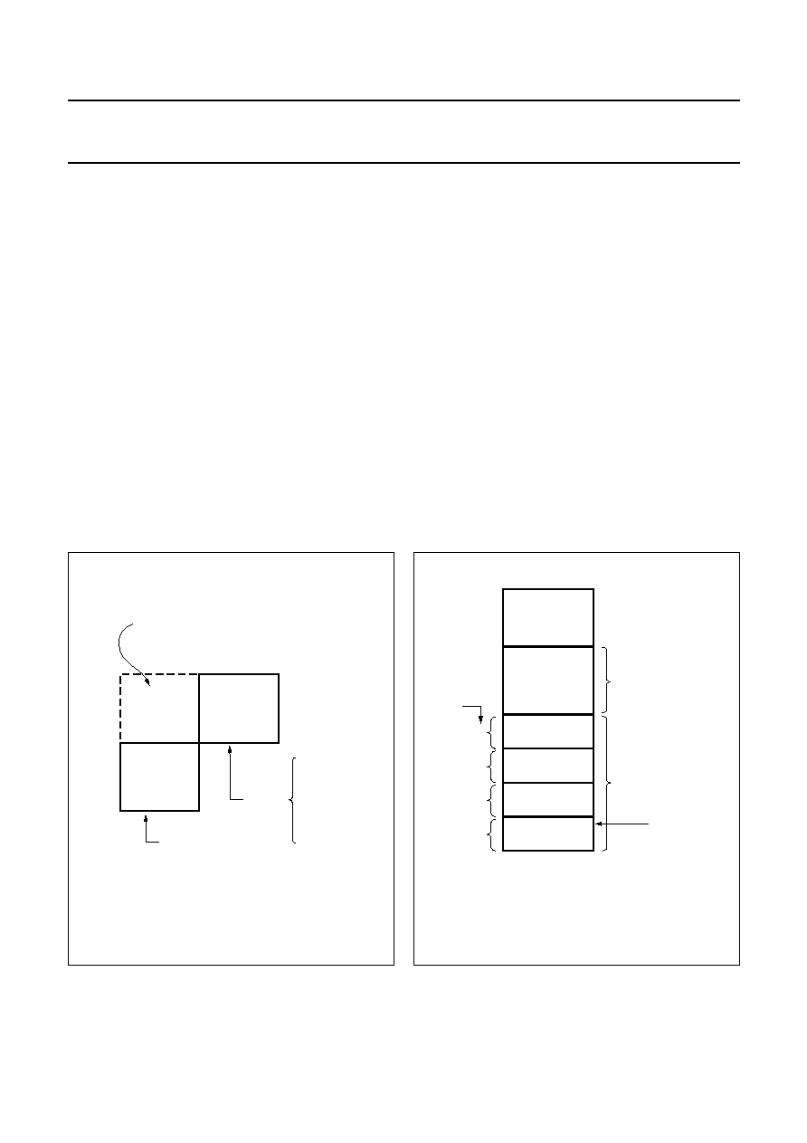
2001 Jun 19
63
Philips Semiconductors
Product specification
80C51 Ultra Low Power (ULP) telephony controller
P83CL882
6.10
Internal Data Memory
Internal Data Memory is mapped in Fig.31. The memory
space is divided into three blocks, which are referred to as
the lower 128, the upper 128, and SFR space.
Internal Data Memory addresses are always one byte
wide, which implies an address space of only 256 bytes.
However, the addressing modes for internal RAM can in
fact accommodate 384 bytes, using a simple trick. Direct
addresses higher than 7FH access one memory space,
and indirect addresses higher than 7FH access a different
memory space. Thus Fig.31 shows the upper 128 and
SFR space occupying the same block of addresses,
80H through FFH, although they are physically separate
entities.
The lower 128 bytes of RAM are present in all 80C51
devices as mapped in Fig.32. The lowest 32 bytes are
grouped into 4 banks of 8 registers. Program instructions
call out these registers as R0 through R7. Two bits in the
Program Status Word (PSW) select which register bank is
in use.
This allows more efficient use of code space, since register
instructions are shorter than instructions that use direct
addressing. The next 16 bytes above the register banks
form a block of bit-addressable memory space. The 80C51
instruction set includes a wide selection of single-bit
instructions, and the 128 bits in this area can be directly
addressed by these instructions. The bit addresses in this
area are 00H through 7FH. All of the bytes in the lower 128
can be accessed by either direct or indirect addressing.
The upper address space of 128 bytes is overlaid with the
128-byte SFR address space. When using indirect
addressing the internal data memory is accessed but
when using direct addressing the SFR memory space is
accessed. Figure 31 shows the overlay of internal Data
Memory and SFR memory space. SFRs include the Port
latches, timers, peripheral controls, etc. Sixteen addresses
in SFR space are both byte-and bit-addressable. The
bit-addressable SFRs are those whose address ends
in 0H or 8H.
MBL261
Accessible
by Indirect
Addressing
only
upper
128
lower
128
Accessible
by Direct
and Indirect
Addressing
SFR
Memory
Space
Ports,
Status and
Control Bits,
Timers,
Registers,
Stack Pointer,
Accumulator,
etc.
FFH
7FH
0
80H
FFH
80H
Accessible
by Direct
Addressing
RAM data memory
In the 83CL882 only 128 bytes of RAM are implemented,
therefore the upper 128 bytes are mapped to the
lower memory block
Fig.31 Internal Data Memory.
MGT303
00
bank
select
bits in
PSW
07H
0
01
0FH
08H
10
17H
10H
11
1FH
18H
2FH
20H
7FH
bit-addressable space
(bit addresses 0 to 7FH)
4 banks of 8 registers
R0 to R7
reset value of
Stack Pointer
Fig.32 The lower 128 bytes of internal Data
Memory.

2001
Jun
19
64
Philips Semiconductors
Product specification
80C51 Ultr
a Lo
w P
o
w
e
r
(ULP) telephon
y controller
P83CL882
6.11
Special Function Registers overview
Table 77 SFRs overview
An empty field (
-
) indicates a bit that can be read or written to by software.
ADDR
(HEX)
R/W
BIT
ADDRESSABLE
NAME
7
6
5
4
3
2
1
0
RESET
VALUE
80
RW
yes
P0
-
-
-
-
-
-
-
-
EFH
81
RW
-
SP
-
-
-
-
-
-
-
-
07H
82
RW
-
DPL
-
-
-
-
-
-
-
-
00H
83
RW
-
DPH
-
-
-
-
-
-
-
-
00H
87
RW
-
PCON
-
-
-
-
-
-
PD
IDL
00H
88
RW
yes
TCON
TF1
TR1
TF0
TR0
IE1
IT1
IE0
IT0
00H
89
RW
-
TMOD
GATE
C/T
M1
M0
GATE
C/T
M1
M0
00H
8A
RW
-
TL0
-
-
-
-
-
-
-
-
00H
8B
RW
-
TL1
-
-
-
-
-
-
-
-
00H
8C
RW
-
TH0
-
-
-
-
-
-
-
-
00H
8D
RW
-
TH1
-
-
-
-
-
-
-
-
00H
8E
RW
-
P0CFGA
-
-
-
-
-
-
-
-
F3H
8F
RW
-
P0CFGB
-
-
-
-
-
-
-
-
00H
90
RW
yes
P1
-
-
-
-
-
-
-
-
FFH
9E
RW
-
P1CFGA
-
-
-
-
-
-
-
-
FFH
9F
RW
-
P1CFGB
-
-
-
-
-
-
-
-
00H
A5
RW
-
WDCON
COND
WD3
WD2
WD1
WD0
MSKPOL
-
LD
00H
A6
RW
-
WDTIM
-
-
-
-
-
-
-
-
00H
A8
RW
yes
IEN0/IE
EA
ET2
ES1
-
ET1
EX1
ET0
EX0
00H
B0
RW
yes
P3
-
-
-
-
-
-
-
-
FFH
B4
RW
-
SYSCON
T1SRC1 T1SRC0 T0SRC1
T0SRC0
-
-
SELECT
XTM
00H
B8
RW
yes
IP0
-
PT2
PS1
-
PT1
PX1
PT0
PX0
00H
BE
RW
-
P3CFGA
-
-
-
-
-
-
-
-
FFH
BF
RW
-
P3CFGB
-
-
-
-
-
-
-
-
00H
C0
RW
yes
IRQ1
IQ9
IQ8
IQ7
IQ6
IQ5
IQ4
IQ3
IQ2
00H
C8
RW
yes
T2CON
T2F
EXF2
-
-
EXEN2
TR2
C/T2
CP/RL2
00H
C9
RW
-
T2MOD
-
-
-
-
-
T2RD
C/T2OE
CP/DCEN
00H
CA
RW
-
T2RCL
-
-
-
-
-
-
-
-
00H

2001
Jun
19
65
Philips Semiconductors
Product specification
80C51 Ultr
a Lo
w P
o
w
e
r
(ULP) telephon
y controller
P83CL882
Notes
1. This bit is read only.
2. This bit is set to logic 1 by hardware; can only be cleared by software.
CB
RW
-
T2RCH
-
-
-
-
-
-
-
-
00H
CC
RW
-
T2L
-
-
-
-
-
-
-
-
00H
CD
RW
-
T2H
-
-
-
-
-
-
-
-
00H
D0
RW
yes
PSW
CY
AC
F0
RS1
RS0
OV
-
P
(1)
00H
D1
RW
-
MBUF
D7
D6
D5
D4
D3
D2
D1
D0
00H
D2
RW
-
MSTAT
-
-
MRF
(1)
MRE
(1)
MRP
(1)
MRL
(1)
MTI
MRI
(2)
00H
D3
RW
-
MCON
MPR3
MPR2
MPR1
MPR0
MB1
MB0
MTEN
MREN
00H
D8
RW
yes
S1CON
CR2
ENS1
STA
STO
SI
AA
CR1
CR0
00H
D9
R
-
S1STA
SC4
SC3
SC2
SC1
SC0
0
0
0
F8H
DA
RW
-
S1DAT
-
-
-
-
-
-
-
-
00H
DB
RW
-
S1ADR
SLA6
SLA5
SLA4
SLA3
SLA2
SLA1
SLA0
GC
00H
DD
RW
-
WKCON
-
-
-
-
-
-
-
-
00H
E0
RW
yes
ACC
-
-
-
-
-
-
-
-
00H
E1
RW
-
ISE1
ISE9
ISE8
ISE7
ISE6
ISE5
ISE4
ISE3
ISE2
00H
E8
RW
yes
IEN1
EX9
EX8
EX7
EX6
EX5
EX4
EX3
EX2
00H
E9
RW
-
IX1
IX9
IX8
IX7
IX6
IX5
IX4
IX3
IX2
00H
F0
RW
yes
B
-
-
-
-
-
-
-
-
00H
F1
RW
-
IEN2
EWDI
EADI
EKPI
-
ELVD
-
EMTI
EMRI
00H
F3
RW
-
PRESC
EXTCK
AUXSW
SYNC
-
-
-
-
-
00H
F8
RW
yes
IP1
PX7
PX6
PX5
PX6
PX5
PX4
PX3
PX2
00H
F9
RW
-
IP2
PWDI
PADI
PKPI
-
PLVD
-
PMTI
PMRI
00H
ADDR
(HEX)
R/W
BIT
ADDRESSABLE
NAME
7
6
5
4
3
2
1
0
RESET
VALUE
2001 Jun 19
66
Philips Semiconductors
Product specification
80C51 Ultra Low Power (ULP) telephony controller
P83CL882
7
INSTRUCTION SET
The asynchronous 80C51 family uses a powerful instruction set which permits the expansion of on-chip CPU peripherals
and optimizes power consumption in idle and active modes as well as byte efficiency and execution speed. Typical
execution times and energy consumption at room temperature (T
amb
= 25
∞
C) and V
DD
= 3.0 V are given in Table 78.
Remark: For most opcodes the numbers for execution speed and energy are also strongly dependent on the data (ADD,
SUBB, DEC, INC, MUL, DIV, DA conditional jumps etc.) and the operand address (CPU internal SFRs or SFRs in
a peripheral block).
Table 78 Instruction set
MNEMONIC
DESCRIPTION
BYTES
EXEC.
TIME
(1)
(
µ
s)
ENERGY
(1)
(nJ)
OPCODE
(HEX)
Arithmetic operations
ADD
A, Rn
add register to A
1
0.20
1.13
2*
ADD
A, direct
add direct byte to A
2
0.24
1.68
25
ADD
A, @ Ri
add indirect RAM to A
1
0.21
1.36
26 and 27
ADD
A, #data
add immediate data to A
2
0.23
1.40
24
ADDC
A, Rn
add register to A with carry flag
1
0.20
1.14
3*
ADDC
A, direct
add direct byte to A with carry flag
2
0.25
1.68
35
ADDC
A, @Ri
add indirect RAM to A with carry flag
1
0.21
1.37
36 and 37
ADDC
A, #data
add immediate data to A with carry flag
2
0.23
1.45
34
SUBB
A, Rn
subtract register from A with borrow
1
0.20
1.13
9*
SUBB
A, direct
subtract direct byte from A with borrow
2
0.24
1.69
95
SUBB
A, @Ri
subtract indirect RAM from A with borrow
1
0.21
1.36
96 and 97
SUBB
A, #data
subtract immediate data from A with borrow
2
0.23
1.43
94
INC
A
increment A
1
0.17
0.79
04
INC
Rn
increment register
1
0.18
1.16
0*
INC
direct
increment direct byte
2
0.22
1.75
05
INC
@Ri
increment indirect RAM
1
0.19
1.35
06 and 07
DEC
A
decrement A
1
0.17
0.81
14
DEC
Rn
decrement register
1
0.18
1.17
1*
DEC
direct
decrement direct byte
2
0.22
1.75
15
DEC
@Ri
decrement indirect RAM
1
0.19
1.38
16 and 17
INC
DPTR
increment data pointer
1
0.15
0.78
A3
MUL
AB
multiply A and B
1
0.15
0.70
A4
DIV
AB
divide A by B
1
0.73
3.58
84
DA
A
decimal adjust A
1
0.17
0.74
D4
Logic operations
ANL
A, Rn
AND register to A
1
0.20
1.24
5*
ANL
A, direct
AND direct byte to A
2
0.30
1.91
55
ANL
A, @Ri
AND indirect RAM to A
1
0.21
1.44
56 and 57
ANL
A, #data
AND immediate data to A
2
0.23
1.50
54

2001 Jun 19
67
Philips Semiconductors
Product specification
80C51 Ultra Low Power (ULP) telephony controller
P83CL882
ANL
direct, A
AND A to direct byte
2
0.26
1.96
52
ANL
direct, #data
AND immediate data to direct byte
3
0.28
2.41
53
ORL
A, Rn
OR register to A
1
0.29
1.71
4*
ORL
A, direct
OR direct byte to A
2
0.29
1.72
45
ORL
A, @Ri
OR indirect RAM to A
1
0.19
1.27
46 and 47
ORL
A, #data
OR immediate data to A
2
0.21
1.23
44
ORL
direct, A
OR A to direct byte
2
0.24
1.78
42
ORL
direct, #data
OR immediate data to direct byte
3
0.27
2.16
43
XRL
A, Rn
exclusive-OR register to A
1
0.29
1.72
6*
XRL
A, direct
exclusive-OR direct byte to A
2
0.29
1.72
65
XRL
A, @Ri
exclusive-OR indirect RAM to A
1
0.19
1.31
66 and 67
XRL
A, #data
exclusive-OR immediate data to A
2
0.21
1.33
64
XRL
direct, A
exclusive-OR A to direct byte
2
0.24
1.83
62
XRL
direct, #data
exclusive-OR immediate data to direct byte
3
0.27
2.27
63
CLR
A
clear A
1
0.14
0.71
E4
CPL
A
complement A
1
0.15
0.93
F4
RL
A
rotate A left
1
0.15
0.73
23
RLC
A
rotate A left through the carry flag
1
0.15
0.74
33
RR
A
rotate A right
1
0.17
0.82
03
RRC
A
rotate A right through the carry flag
1
0.15
0.73
13
SWAP
A
swap nibbles within A
1
0.14
0.71
C4
Data transfer
MOV
A, Rn
move register to A
1
0.15
0.89
E*
MOV
A, direct
move direct byte to A
2
0.19
1.49
E5
MOV
A, @Ri
move indirect RAM to A
1
0.16
1.13
E6 and E7
MOV
A, #data
move immediate data to A
2
0.21
1.85
74
MOV
Rn, A
move A to register
1
0.13
0.86
F*
MOV
Rn, direct
move direct byte to register
2
0.23
1.90
A*
MOV
Rn, #data
move immediate data to register
2
0.16
1.28
7*
MOV
direct, A
move A to direct byte
2
0.18
1.47
F5
MOV
direct, Rn
move register to direct byte
2
0.21
1.68
8*
MOV
direct, direct
move direct byte to direct byte
3
0.25
2.22
85
MOV
direct, @Ri
move indirect RAM to direct byte
2
0.22
1.92
86 and 87
MOV
direct, #data
move immediate data to direct byte
3
0.21
1.85
75
MOV
@RI, A
move A to indirect RAM
1
0.14
1.01
F6 and F7
MOV
@Ri, direct
move direct byte to indirect RAM
2
0.25
2.09
A6 and A7
MOV
@Ri, #data
move immediate data to indirect RAM
3
0.11
0.92
76 and 77
MOV
DPTR,
#data 16
load data pointer with a 16-bit constant
3
0.20
1.58
90
MNEMONIC
DESCRIPTION
BYTES
EXEC.
TIME
(1)
(
µ
s)
ENERGY
(1)
(nJ)
OPCODE
(HEX)

2001 Jun 19
68
Philips Semiconductors
Product specification
80C51 Ultra Low Power (ULP) telephony controller
P83CL882
MOVC
A, @A + DPTR move code byte relative to DPTR to A
1
0.31
2.34
93
MOVC
A, @A + PC
move code byte relative to PC to A
1
0.32
2.47
83
MOVX
(2)
A, @Ri
move external RAM (8-bit address) to A
1
-
-
E2 and E3
MOVX
(2)
A, @DPTR
move external RAM (16-bit address) to A
1
-
-
E0
MOVX
(2)
@Ri, A
move A to external RAM (8-bit address)
1
-
-
F2 and F3
MOVX
(2)
@DPTR,A
move A to external RAM (16-bit address)
1
-
-
F0
PUSH
direct
push direct byte onto stack
2
0.26
1.62
C0
POP
direct
pop direct byte from stack
2
0.26
1.66
D0
XCH
A, Rn
exchange register with A
1
0.20
1.35
C*
XCH
A, direct
exchange direct byte with A
2
0.25
1.98
C5
XCH
A, @Ri
exchange indirect RAM with A
1
0.21
1.42
C6 and C7
XCHD
A, @Ri
exchange LOW-order nibble indirect RAM
with A
1
0.19
1.38
D6 and D7
Boolean variable manipulation
CLR
C
clear carry flag
1
0.11
0.64
C3
CLR
bit
clear direct bit
2
0.24
1.51
C2
SETB
C
set carry flag
1
0.11
0.65
D3
SETB
bit
set direct bit
2
0.24
1.71
D2
CPL
C
complement carry flag
1
0.12
0.68
B3
CPL
bit
complement direct bit
2
0.23
1.59
B2
ANL
C, bit
AND direct bit to carry flag
2
0.21
1.30
82
ANL
C, /bit
AND complement of direct bit to carry flag
2
0.23
1.55
B0
ORL
C, bit
OR direct bit to carry flag
2
0.21
1.33
72
ORL
C, /bit
OR complement of direct bit to carry flag
2
0.23
1.54
A0
MOV
C, bit
move direct bit to carry flag
2
0.22
1.34
A2
MOV
bit, C
move carry flag to direct bit
2
0.24
1.52
92
Program and machine control
ACALL
addr11
absolute subroutine call
2
0.40
2.64
∑
1 addr
LCALL
addr16
long subroutine call
3
0.45
3.09
12
RET
return from subroutine
1
0.20
1.03
22
RETI
return from interrupt
1
0.43
3.01
32
AJMP
addr11
absolute jump
2
0.29
1.76
1 addr
LJMP
addr16
long jump
3
0.32
2.14
02
SJMP
rel
short jump (relative address)
2
0.26
1.50
80
JMP
@A+DPTR
jump indirect relative to the DPTR
1
0.46
2.63
73
JZ
rel
jump if A is zero
2
0.29
1.62
60
JNZ
rel
jump if A is not zero
2
0.26
1.34
70
JC
rel
jump if carry flag is set
2
0.24
1.23
40
JNC
rel
jump if carry flag is not set
2
0.29
1.61
50
MNEMONIC
DESCRIPTION
BYTES
EXEC.
TIME
(1)
(
µ
s)
ENERGY
(1)
(nJ)
OPCODE
(HEX)

2001 Jun 19
69
Philips Semiconductors
Product specification
80C51 Ultra Low Power (ULP) telephony controller
P83CL882
Notes
1. Verified on sampling base.
2. Only applicable if XRAM is present on-chip (no external access possible).
Table 79 Notation for data addressing modes
Table 80 Hexadecimal opcode cross-reference
JB
bit, rel
jump if direct bit is set
3
0.31
1.90
20
JNB
bit, rel
jump if direct bit is not set
3
0.36
2.29
30
JBC
bit, rel
jump if direct bit is set and clear bit
3
0.36
2.25
10
CJNE
A, direct, rel
compare direct to A and jump if not equal
3
0.34
2.27
B5
CJNE
A, #data, rel
compare immediate to A and jump if not
equal
3
0.35
2.38
B4
CJNE
Rn, #data, rel
compare immediate to register and jump if
not equal
3
0.35
2.59
B*
CJNE
Ri, #data, rel
compare immediate to indirect and jump if
not equal
3
0.36
2.82
B6 and B7
DJNZ
Rn, rel
decrement register and jump if not zero
2
0.33
2.29
D*
DJNZ
direct, rel
decrement direct and jump if not zero
3
0.39
2.89
D5
NOP
no operation
1
0.11
0.63
00
SYMBOL
DESCRIPTION
R
n
working registers R0 to R7
direct
128 internal RAM locations and any special function register (SFR)
R
i
indirect internal RAM location addressed by register R0 or R1
#data
8-bit constant included in instruction
#data 16
16-bit constant included as bytes 2 and 3 of instruction
bit
direct addressed bit in internal RAM or SFR
addr16
16-bit destination address; used by LCALL and LJMP; the branch will be anywhere within the
64 kbytes program memory address space
addr11
11-bit destination address; used by ACALL and AJMP. The branch will be within the same 2-kbyte
page of program memory as the first byte of the following instruction
rel
signed (two's complement) 8-bit offset byte; used by SJMP and all conditional jumps; range is
-
128 to +127 bytes relative to first byte of the following instruction
SYMBOL
DESCRIPTION
*
8, 9, A, B, C, D, E and F
∑
11, 31, 51, 71, 91, B1, D1 and F1
01, 21, 41, 61, 81, A1, C1 and E1
MNEMONIC
DESCRIPTION
BYTES
EXEC.
TIME
(1)
(
µ
s)
ENERGY
(1)
(nJ)
OPCODE
(HEX)
2001
Jun
19
70
Philips Semiconductors
Product specification
80C51 Ultr
a Lo
w P
o
w
e
r
(ULP) telephon
y controller
P83CL882
This text is here in white to force landscape pages to be rotated correctly when browsing through the pdf in the Acrobat reader.This text is here in
_
white to force landscape pages to be rotated correctly when browsing through the pdf in the Acrobat reader.This text is here inThis text is here in
white to force landscape pages to be rotated correctly when browsing through the pdf in the Acrobat reader. white to force landscape pages to be ...
7.1
Instruction map
a
ndbook, full pagewidth
first hexadecimal character of opcode
MOVC
A,@A+DPTR
second hexadecimal character of opcode
0
1
2
3
4
5
6
7
8
9
A
B
C
D
E
F
0
1
2
3
4
5
6
7
8
9
A
B
C
D
E
F
NOP
JBC
bit,rel
JB
bit,rel
JNB
bit,rel
JC
rel
JNC
rel
JZ
rel
JNZ
rel
SJMP
rel
MOV
DPTR,#data 16
ORL
C,/bit
ANL
C,/bit
PUSH
direct
POP
direct
MOVX
A,@DPTR
MOVX
@DPTR,A
AJMP
addr11
ACALL
addr11
AJMP
addr11
ACALL
addr11
AJMP
addr11
ACALL
addr11
AJMP
addr11
ACALL
addr11
AJMP
addr11
ACALL
addr11
AJMP
addr11
ACALL
addr11
AJMP
addr11
ACALL
addr11
AJMP
addr11
ACALL
addr11
LJMP
addr16
LCALL
addr16
RET
RETI
ORL
direct,A
ANL
direct,A
XRL
direct,A
ORL
C,bit
ANL
C,bit
MOV
bit,C
MOV
C,bit
CPL
bit
CLR
bit
SETB
bit
0
1
0
1
MOVX @Ri,A
MOVX A,@Ri
RR
A
RRC
A
RLC
A
ORL
direct,#data
ANL
direct,#data
XRL
direct,#data
JMP
@A+DPTR
MOVC
A,@A+PC
INC
DPTR
CPL
C
CLR
C
SETB
C
RL
A
INC
A
DEC
A
ADD
A,#data
ADDC
A,#data
ORL
A,#data
ANL
A,#data
XRL
A,#data
MOV
A,#data
DIV
AB
SUBB
A,#data
MUL
AB
CJNE
A,#data,rel
SWAP
A
DA
A
CLR
A
CPL
A
INC
direct
DEC
direct
ADD
A,direct
ADDC
A,direct
ORL
A,direct
ANL
A,direct
XRL
A,direct
MOV
direct,#data
MOV
direct,direct
SUBB
A,direct
CJNE
A,direct,rel
XCH
A,direct
DJNZ
direct,rel
MOV
A,direct
MOV
direct,A
*
0
1
0
1
2
3
4
5
6
7
0
1
0
1
2
3
4
5
6
7
0
1
0
1
2
3
4
5
6
7
0
1
0
1
2
3
4
5
6
7
0
1
0
1
2
3
4
5
6
7
0
1
0
1
2
3
4
5
6
7
0
1
0
1
2
3
4
5
6
7
0
1
0
1
2
3
4
5
6
7
0
1
0
1
2
3
4
5
6
7
0
1
0
1
2
3
4
5
6
7
0
1
0
1
2
3
4
5
6
7
0
1
0
1
2
3
4
5
6
7
0
1
0
1
2
3
4
5
6
7
0
1
0
1
2
3
4
5
6
7
0
1
0
1
2
3
4
5
6
7
0
1
0
1
2
3
4
5
6
7
INC@Ri
DEC@Ri
ADD A,@Ri
ADDC A,@Ri
ORL A,@Ri
ANL A,@Ri
XRL A,@Ri
MOV @Ri,#data
MOV direct,@Ri
SUBB A,@Ri
MOV @Ri,direct
CJNE @Ri,#data,rel
XCH A,@Ri
XCHD A,@Ri
MOV A,@Ri
MOV @Ri,A
INC Rn
DEC Rn
ADD A,Rn
ADDC A,Rn
ORL A,Rn
ANL A,Rn
XRL A,Rn
MOV direct,Rn
SUBB A, Rn
MOV Rn,direct
CJNE Rn,#data,rel
XCH A,Rn
DJNZ Rn,rel
MOV A,Rn
MOV Rn,A
MOV Rn,#data
* MOV A, ACC is not a valid instruction.
MGL457
Fig.33 Instruction map.

2001 Jun 19
71
Philips Semiconductors
Product specification
80C51 Ultra Low Power (ULP) telephony controller
P83CL882
8
APPLICATION INFORMATION
8.1
Introduction
This chapter presents some information about how to use
the P83CL882 in an application. It is not intended to
replace the application notes but serves as a quick help
when starting to work with the Philips Ultra Low Power
handshake microcontrollers. There are some important
improvements between the silicon in plastic packages and
the Metalink EH emulator system which are described
here. Furthermore, some hints on software development
and power consumption are given to help the user take
advantage of the full benefits of the handshake CPU.
8.2
Differences between P83CL882 and the
Metalink EH emulation system
∑
The SYSCON SFR does not exist on the emulator
system
∑
On the emulator the oscillator can only be used in
normal mode which is the default start-up mode of the
P83CL882. The hysteresis input comparator does not
exist
∑
The clock source of the Timer 0 and 1 is always f
psc
on
the emulator system. The timers can be used as
counters, counting from external pin T1 or T0 but this is
not possible in Power-down mode.
∑
The interrupts T0 and T1 can cause on the emulator
only a wake-up from idle and not from power-down
∑
Prescaler bits PRESC[7:5] are not available on the
emulator; therefore the synchronous mode and clock
out functionality is not present
∑
MSK polarity cannot be inverted on the emulator
∑
INT1 interrupt is on the emulator version present on
P3.3 where it is mapped on P3.1 on the P83CL882
∑
The clock output on P1.4 does not exist on the emulator.
8.3
The asynchronous handshake CPU
As the CPU of the P83CL882 is built in asynchronous
technology (hand-shake mechanism) some properties are
singular to it in comparison to standard synchronous
80C51 controllers:
∑
The CPU itself does not need a clock for code execution
∑
The performance (MIPs) is not dependent on oscillator
frequency but strongly related to V
DD
, temperature,
silicon parameters and type of software. It always runs
at the maximum speed determined by the external
influences above. Therefore, it operates also with the
maximum power consumption in the minimum time.
Generally the lower the temperature and the higher the
V
DD
the faster the CPU runs. Details on instruction
speed and energy consumption per instruction can be
found in Chapter 7.
Because of the above mentioned properties some hints
are given for using this controller in any kind of application
in an efficient way.
∑
Due to the high CPU performance, independent of clock
frequency, certain functions (e.g. serial or customized
interfaces) can be built in software in a very efficient and
flexible way.
∑
In classic 80C51 software the user (software engineer)
was able to rely on cycle-timing for wait-loops,
synchronisation in the system or similar usage (e.g.
NOP instruction for waiting one machine cycle). When
using the asynchronous CPU wait-loops should be
implemented by starting a timer and putting the CPU in
Idle mode in order to wait for an interrupt. Significant
power reduction and a much more robust software will
be obtained. If in an application the instruction counter is
needed Timer 0 or 1 can be used with the instruction
request signal connected to the clock source input.
∑
One should avoid using `wait-until'-loops (SFR polling).
This would lead to maximum CPU-load resulting in very
high current consumption. The CPU should always be
used as an event driven machine waiting for interrupts.
After an activity the device must be entered in Idle or
Power-down mode as fast as possible, the current is
then reduced down to leakage. The device provides
flexible means (interrupts, timer, counters) for
a recovery from these power reduction modes.

2001 Jun 19
72
Philips Semiconductors
Product specification
80C51 Ultra Low Power (ULP) telephony controller
P83CL882
9
HOW TO ESTIMATE P83CL882 POWER
CONSUMPTION
9.1
General
Due to the use of the Philips unique asynchronous
technology within the CPU, the power estimation must be
done by taking into account several circumstances.
To have an accurate power estimation the application
must be well known. This especially means that all (or the
most significant) application modes (e.g. idle or operation
modes) are known and their weight or contribution ≠ what
is done when with which occurrence ≠ can be estimated
precise enough.
9.2
Modes
9.2.1
P
OWER
-
DOWN MODE
In Power-down there is no circuitry active which is drawing
current. The CPU, the oscillator, the clock tree and the
peripheral functions are switched off except Timer 0 and 1
which can function as counter in Power-down mode. The
device can be woken-up by an interrupt.
In this mode the power consumption is only dependent on
outside activity (port toggling, gate-current) and leakage
(see Fig.34).
9.2.2
I
DLE MODE
In Idle mode the oscillator (if enabled), the clock tree and
the enabled peripheral functions are running.
The peripheral functions are fixed to the peripheral clock
(f
per
or f
psc
). In Figs 39, 39 and 39 one can see the
behaviour of the idle current with no peripheral functions
switched on.
9.2.3
O
PERATING MODE
In operating mode the CPU, the oscillator, the clock tree
and the enabled peripheral functions are running. While
the peripheral functions are fixed to the peripheral clock
(f
per
or f
psc
) the CPU is completely free running. In plain
words: it does one instruction after the other without any
clocking nor timing scheme. In addition to that and to make
code execution faster following instruction is pre-fetched
while an instruction is being executed.
9.3
Examples of power consumption estimation
A rough estimation of device power consumption can be made by an add-up of the Power-down mode current, Idle mode
current, enabled peripheral function(s) current and estimated CPU processing load times mean value of operating
current:
I
DD(pd)
+ I
DD(id)
+ I
periphery
+ CPU load
◊
I
DD(op)
.
Assume an application part where the device is 50% in idle, during idle for total 40% a peripheral function is running,
for 20% the CPU is active and the rest is power-down state. Then the averaged power consumption can roughly be
calculated as follows:
I
average
= (100%
◊
I
DD(pd)
) + (50%
◊
I
DD(id)
) + (40%
◊
I
periphery
) + (20%
◊
I
DD(op)
).
When the number of instructions within an application part and its execution time is known, then the CPU processing
load can be estimated as shown below. The CPU performance (in Mips) is given by the supply voltage:
CPU processing load
100%
number of instructions
time (seconds)
-----------------------------------------------------------
10
6
≠
CPU performance (in Mips)
------------------------------------------------------------------------
◊
◊
=
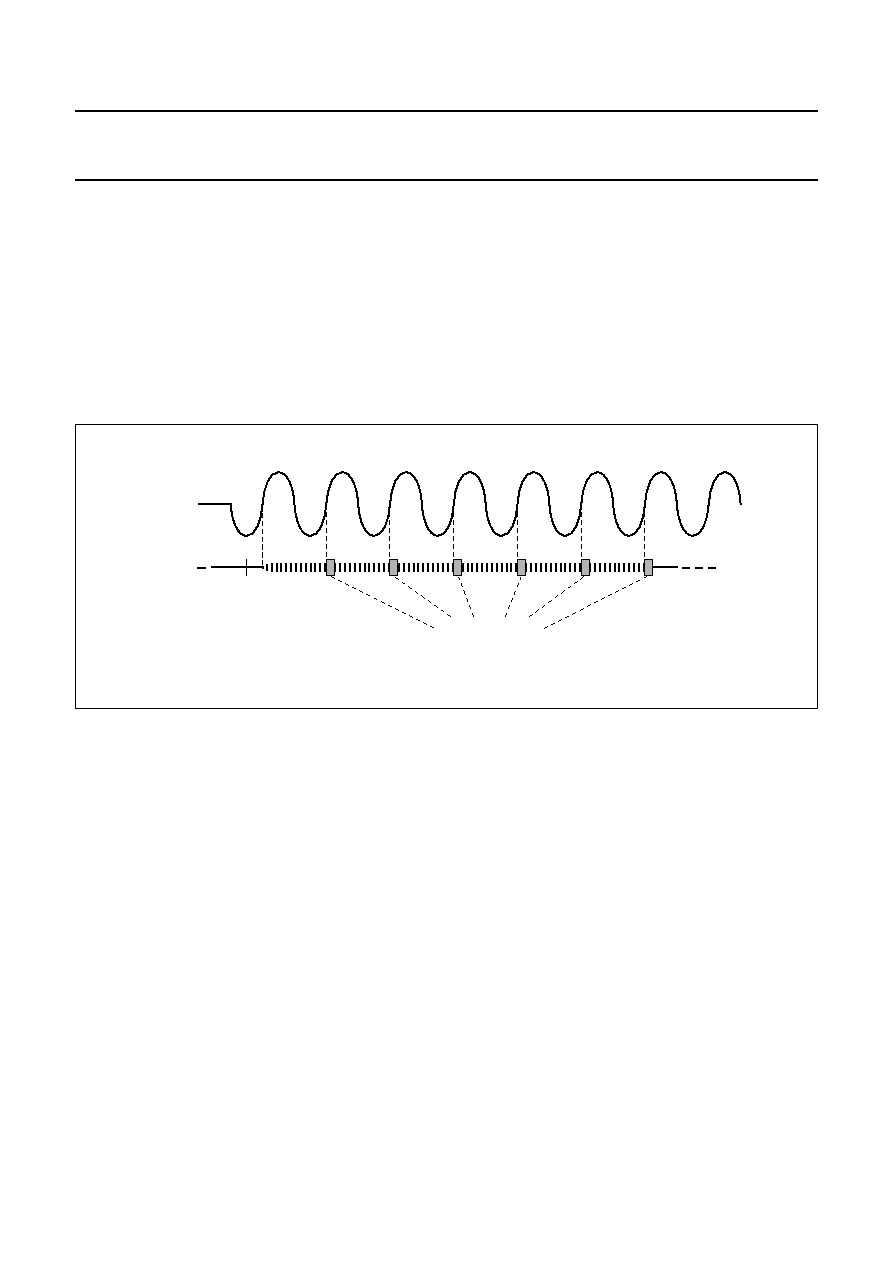
2001 Jun 19
73
Philips Semiconductors
Product specification
80C51 Ultra Low Power (ULP) telephony controller
P83CL882
9.3.1
E
XAMPLE OF RING
-
DETECTION
Typically a ring-detection is done by a time measurement using a timer. The device is activated by an external interrupt
(e.g. AC on the A/B line), the oscillator runs up and the device carries out the time measurement with a timer.
In this example it can be assumed that to read the timer contents, decide whether an external ringer should be enabled
or not, to restart the timer and then go into Idle mode is around 30 instructions. Assuming a ringing frequency of about
25 Hz and a device supply voltage of 3.0 V this gives a CPU performance of about 4.5 Mips.
The CPU processing load is then:
From the calculation above it can be seen that the idle current will be dominant in this application part.
100%
30 instructions
◊
25 Hz
◊
4.5 Mips
1000000
◊
----------------------------------------------------------------------------------
0.017%
MGT314
A/B line
Activity
CPU operation
IDLE
IDLE
IDLE
IDLE
IDLE
IDLE
Fig.34 Ring-detection sequence.
2001 Jun 19
74
Philips Semiconductors
Product specification
80C51 Ultra Low Power (ULP) telephony controller
P83CL882
10 LIMITING VALUES
According to the Absolute Maximum Ratings System (IEC 60134); note 1.
Notes
1. Parameters are valid over operating temperature range unless otherwise specified. All voltages are with respect to
V
SS
unless otherwise specified.
2. May not exceed the limiting value for V
DD
.
3. According to SNW-FQ-302A: C = 100 pF; R = 1.5 kW.
4. According to SNW-FQ-302B: C = 200 pF; L = 0.75 mH.
SYMBOL
PARAMETER
CONDITIONS
MIN.
MAX.
UNIT
V
DD
supply voltage
-
0.5
+4.6
V
V
I
input voltage
note 2
-
0.5
V
DD
+ 0.5 V
I
I/O
maximum sink/source current for each
input/output pin
-
±
10
mA
I
DD
maximum supply current for any supply pin
-
50
mA
V
es
electrostatic handling voltage
human body model; note 3
-
2000
V
machine model; note 4
-
175
V
P
tot
total power dissipation
-
100
mW
T
stg
storage temperature
-
55
+125
∞
C
T
amb
operating ambient temperature (for all
devices)
-
25
+70
∞
C

2001 Jun 19
75
Philips Semiconductors
Product specification
80C51 Ultra Low Power (ULP) telephony controller
P83CL882
11 CHARACTERISTICS
V
DD
= 1.8 to 3.6 V; V
SS
= 0 V; f
xtal
= 4 MHz; T
amb
=
-
25 to +70
∞
C; unless otherwise specified.
SYMBOL
PARAMETER
CONDITIONS
MIN.
TYP.
MAX.
(1)
UNIT
Supply
V
DD
supply voltage
operating
1.8
(2)
-
3.6
V
RAM data retention
1.0
-
3.6
V
I
DD
operating supply current
V
DD
= 3 V; T
amb
= 25
∞
C;
at 100% CPU load
note 3
-
-
4.5
mA
notes 4 and 5
-
3.0
-
mA
I
DD(id)
supply current Idle mode
V
DD
= 3 V; external clock;
note 6
-
60
75
µ
A
V
DD
= 3 V; T
amb
= 25
∞
C;
crystal connected; note 5
-
300
-
µ
A
I
DD(pd)
supply current Power-down mode V
DD
= 3 V; T
amb
= 25
∞
C;
note 7
-
0.1
-
µ
A
V
DD
= 3 V; T
amb
= 70
∞
C;
note 7
-
-
4.5
µ
A
I
DD(block)
supply current per block:
V
DD
= 3 V; T
amb
= 25
∞
C;
note 8
MSK modem
-
14
-
µ
A
Watchdog Timer
-
2
-
µ
A
I
2
C-bus
-
30
-
µ
A
Timer 2
-
4
-
µ
A
Timer 0 or 1
-
10
-
µ
A
Performance
f
XTAL1
external clock input frequency
notes 5 and 9
DC
-
12
MHz
CPU
perf
CPU performance
T
amb
= 25
∞
C;
notes 4 and 5
V
DD
= 1.8 V
-
2.6
-
Mips
V
DD
= 3.0 V
-
4.5
-
Mips
CPU
eff
CPU efficiency
T
amb
= 25
∞
C;
notes 4 and 5
V
DD
= 1.8 V
-
1910
-
Mips/W
V
DD
= 3.0 V
-
555
-
Mips/W

2001 Jun 19
76
Philips Semiconductors
Product specification
80C51 Ultra Low Power (ULP) telephony controller
P83CL882
Inputs (Ports, MIN and RST)
V
IL
LOW-level input voltage
notes 10 and 11
0
-
0.2V
DD
V
V
IH
HIGH-level input voltage
note 10
0.8V
DD
-
V
DD
V
I
IL
LOW-level input current; ports in
standard port configuration
V
IN
= 0.4 V; note 12;
see Fig.44
-
20
50
µ
A
I
IL(T)
LOW-level input current;
HIGH-to-LOW transition; ports in
standard port configuration
V
IN
= 0.5V
DD
; note 12;
see Fig.44
-
200
1000
µ
A
I
LI
input leakage current; ports in
open-drain or high-impedance
input configuration
V
SS
V
I
V
DD
-
-
100
nA
Outputs (Ports and RST)
I
OL
LOW-level output current; except
SDA and SCL; note 12
V
DD
= 3.0 V; V
OL
= 0.4 V
4
-
-
mA
V
DD
= 3.0 V; V
OL
= 1.5 V
-
10
-
mA
I
OH
HIGH -level output current;
push-pull configuration only
V
DD
= 3 V;
V
OH
= V
DD
-
0.4 V
4
-
-
mA
V
DD
= 3 V;
V
OH
= V
DD
-
1.5 V
-
10
-
mA
I
RST
RST pull-up resistor current
V
DD
= 3 V;
V
OH
= V
DD
-
0.4 V
0.05
0.1
-
µ
A
V
DD
= 3 V; V
OH
= V
SS
-
0.3
2.5
µ
A
Amplitude Controlled Oscillator (ACO)
f
osc
oscillator frequency
notes 5 and 9
1
-
12
MHz
R
fb
feedback resistance
note 5
-
200
-
k
g
m
transconductance
T
amb
= 25
∞
C; V
DD
= 1.8 V
1.0
-
2.5
mS
T
amb
= 25
∞
C; V
DD
= 3 V
3.0
-
6
mS
C
i(L)(XTAL1)
capacitive input load on XTAL1
-
500
1000
fF
V
XTAL1(p-p)
external clock signal amplitude
on pin XTAL1 (peak-to-peak
value)
in oscillator mode
0.4V
DD
-
V
DD
V
V
DC(XTAL1)
mean value of external clock
signal
in oscillator mode
-
0.5V
DD
-
V
V
IL(XTAL1)
LOW-level input voltage pin
XTAL1
in external clock mode
0
-
0.2V
DD
V
V
IH(XTAL1)
HIGH-level input voltage pin
XTAL1
in external clock mode
0.6V
DD
-
V
DD
V
C
1e
,C
2e
external required load
capacitance on XTAL1 and
XTAL2
-
22
-
pF
SYMBOL
PARAMETER
CONDITIONS
MIN.
TYP.
MAX.
(1)
UNIT

2001 Jun 19
77
Philips Semiconductors
Product specification
80C51 Ultra Low Power (ULP) telephony controller
P83CL882
Notes
1. The measurement of the maximum value is done with all output pins disconnected; V
IL
= V
SS
; V
IH
= V
DD
; RST = V
DD
;
XTAL1 driven with square wave; XTAL2 not connected; all derivative blocks disabled. To see the typical value of
each instruction please consult Table 78 "Instruction set".
2. The minimum operating voltage is the level where VDD is higher than the power-on reset level.
3. For this measurement an instruction was selected which current consumption is around the typical value;
the instruction is: LJMP to ADDR + 03H.
4. The typical operating supply current is evaluated as a mean value over all possible instructions (100% CPU load)
and with a crystal connected.
5. Verified on sampling basis.
6. The Idle mode supply current is measured with all output pins and RST disconnected; V
IL
= V
SS
; V
IH
= V
DD
;
XTAL1 driven with square wave; XTAL2 not connected; all derivative blocks disabled.
7. The Power-down mode supply current is measured with all output pins and RST disconnected; V
IL
= V
SS
; V
IH
= V
DD
;
XTAL1 and XTAL2 not connected.
8. The typical currents are only for the specific block. To calculate the typical power consumption of the microcontroller,
the current consumption of the CPU weighted with the processing must be added. Example: the typical average
current consumption of the microcontroller in operating mode with 10% CPU processing load, Watchdog timer and
MSK active can be calculated as: 10%
◊
I
CPU
+ I
DD(id)
+ I
WD
+ I
MSK
.
9. For some peripheral blocks it could be required to reduce the internal clock frequency with the PSC2 and an
additional divider inside the peripherals. Symbol `f
XTAL1
' is meant for external device clocking and `f
osc
' is meant as
on-chip oscillator frequency.
10. The input threshold voltage of P1.6/SCL and P1.7/SDA meet the I
2
C-bus specification. Therefore, an input voltage
below 0.3V
DD
will be recognized as a logic 0 and an input voltage above 0.7V
DD
will be recognized as a logic 1.
11. Not valid for pins SDA, SCL, RST and MIN.
12. Due to the maximum allowed current, the number of output pins switching at the same time should be limited to one.
2001 Jun 19
78
Philips Semiconductors
Product specification
80C51 Ultra Low Power (ULP) telephony controller
P83CL882
handbook, halfpage
1.5
5
MIPS
0
1
MGW040
2
4
3
2
2.5
3
3.5
4
VDD (V)
Fig.35 Typical CPU performance as a function of
V
DD
, T
amb
= 25
∞
C (mean value over all
instructions).
handbook, halfpage
-
50
100
5
MIPS
0
1
MGW041
2
3
4
-
25
0
25
50
75
Tamb (
∞
C)
Fig.36 Typical CPU performance as a function of
T
amb
, V
DD
= 3 V (mean value over all
instructions).
handbook, halfpage
1.5
2000
MIPS/W
0
400
MGW042
800
1600
1200
2
2.5
3
3.5
4
VDD (V)
Fig.37 Typical CPU efficiency as a function of V
DD
,
T
amb
= 25
∞
C (mean value over all
instructions).
handbook, halfpage
1.5
5
IDD
(mA)
0
1
MGW043
2
4
3
2
2.5
3
3.5
4
VDD (V)
Fig.38 Typical operating current as a function of
V
DD
, T
amb
= 25
∞
C; 100% CPU load (mean
value over all instructions).
2001 Jun 19
79
Philips Semiconductors
Product specification
80C51 Ultra Low Power (ULP) telephony controller
P83CL882
handbook, halfpage
-
50
100
4
IDD
(mA)
0
1
MGW044
2
3
-
25
0
25
50
75
Tamb (
∞
C)
Fig.39 Typical operating current as a function of
T
amb
, V
DD
= 3.0 V; 100% CPU load (mean
value over all instructions).
handbook, halfpage
1.5
IDD
(
µ
A)
0
100
MGW045
200
400
300
2
2.5
3
3.5
4
VDD (V)
Fig.40 Typical Idle current as a function of V
DD
,
T
amb
= 25
∞
C; f
osc
= 4 MHz (crystal).
handbook, halfpage
-
50
100
400
IDD
(
µ
A)
0
100
MGW046
200
300
-
25
0
25
50
75
Tamb (
∞
C)
Fig.41 Typical Idle current as a function of T
amb
,
V
DD
= 3.0 V; f
osc
= 4 MHz (crystal).
handbook, halfpage
0
IDD
(
µ
A)
0
100
MGW047
200
400
300
2
4
6
10
8
12
fosc (MHz)
Fig.42 Typical Idle current as a function of
oscillator (crystal) frequency, V
DD
= 3.0 V;
T
amb
= 25
∞
C.

2001 Jun 19
80
Philips Semiconductors
Product specification
80C51 Ultra Low Power (ULP) telephony controller
P83CL882
0
(1)
(2)
1
2
4
4
3
IDD(pd)
(
µ
A)
1
0
2
3
VDD (V)
MBL262
Fig.43 Typical Power-down current as a function
of V
DD
.
(1) T
amb
= 70
∞
C
(2) T
amb
= 25
∞
C
handbook, full pagewidth
MGL506
0.5VDD
0.3VDD
VDD
0
IIL(T)
IIL
II
500
µ
A
10
µ
A
Fig.44 Port input current.

2001 Jun 19
81
Philips Semiconductors
Product specification
80C51 Ultra Low Power (ULP) telephony controller
P83CL882
12 PACKAGE OUTLINE
UNIT
A1
A2
A3
bp
c
D
(1)
E
(2)
e
HE
L
Lp
Z
y
w
v
REFERENCES
OUTLINE
VERSION
EUROPEAN
PROJECTION
ISSUE DATE
IEC
JEDEC
EIAJ
mm
0.15
0.05
0.95
0.85
0.30
0.19
0.20
0.09
11.10
10.90
6.20
6.00
0.65
8.30
7.90
0.78
0.48
8
0
o
o
0.10
0.10
0.20
1.00
DIMENSIONS (mm are the original dimensions)
Notes
1. Plastic or metal protrusions of 0.15 mm maximum per side are not included.
2. Plastic interlead protrusions of 0.25 mm maximum per side are not included.
0.75
0.50
SOT487-1
MO-153
97-06-11
99-12-27
w
M
bp
D
Z
e
0.25
1
16
32
17
A
A
1
A
2
Lp
detail X
L
(A )
3
H
E
E
c
v
M
A
X
A
y
0
2.5
5 mm
scale
TSSOP32: plastic thin shrink small outline package; 32 leads; body width 6.1 mm;
lead pitch 0.65 mm
SOT487-1
A
max.
1.10
pin 1 index

2001 Jun 19
82
Philips Semiconductors
Product specification
80C51 Ultra Low Power (ULP) telephony controller
P83CL882
13 SOLDERING
13.1
Introduction to soldering surface mount
packages
This text gives a very brief insight to a complex technology.
A more in-depth account of soldering ICs can be found in
our
"Data Handbook IC26; Integrated Circuit Packages"
(document order number 9398 652 90011).
There is no soldering method that is ideal for all surface
mount IC packages. Wave soldering can still be used for
certain surface mount ICs, but it is not suitable for fine pitch
SMDs. In these situations reflow soldering is
recommended.
13.2
Reflow soldering
Reflow soldering requires solder paste (a suspension of
fine solder particles, flux and binding agent) to be applied
to the printed-circuit board by screen printing, stencilling or
pressure-syringe dispensing before package placement.
Several methods exist for reflowing; for example,
convection or convection/infrared heating in a conveyor
type oven. Throughput times (preheating, soldering and
cooling) vary between 100 and 200 seconds depending
on heating method.
Typical reflow peak temperatures range from
215 to 250
∞
C. The top-surface temperature of the
packages should preferable be kept below 220
∞
C for
thick/large packages, and below 235
∞
C for small/thin
packages.
13.3
Wave soldering
Conventional single wave soldering is not recommended
for surface mount devices (SMDs) or printed-circuit boards
with a high component density, as solder bridging and
non-wetting can present major problems.
To overcome these problems the double-wave soldering
method was specifically developed.
If wave soldering is used the following conditions must be
observed for optimal results:
∑
Use a double-wave soldering method comprising a
turbulent wave with high upward pressure followed by a
smooth laminar wave.
∑
For packages with leads on two sides and a pitch (e):
≠ larger than or equal to 1.27 mm, the footprint
longitudinal axis is preferred to be parallel to the
transport direction of the printed-circuit board;
≠ smaller than 1.27 mm, the footprint longitudinal axis
must be parallel to the transport direction of the
printed-circuit board.
The footprint must incorporate solder thieves at the
downstream end.
∑
For packages with leads on four sides, the footprint must
be placed at a 45
∞
angle to the transport direction of the
printed-circuit board. The footprint must incorporate
solder thieves downstream and at the side corners.
During placement and before soldering, the package must
be fixed with a droplet of adhesive. The adhesive can be
applied by screen printing, pin transfer or syringe
dispensing. The package can be soldered after the
adhesive is cured.
Typical dwell time is 4 seconds at 250
∞
C.
A mildly-activated flux will eliminate the need for removal
of corrosive residues in most applications.
13.4
Manual soldering
Fix the component by first soldering two
diagonally-opposite end leads. Use a low voltage (24 V or
less) soldering iron applied to the flat part of the lead.
Contact time must be limited to 10 seconds at up to
300
∞
C.
When using a dedicated tool, all other leads can be
soldered in one operation within 2 to 5 seconds between
270 and 320
∞
C.

2001 Jun 19
83
Philips Semiconductors
Product specification
80C51 Ultra Low Power (ULP) telephony controller
P83CL882
13.5
Suitability of surface mount IC packages for wave and reflow soldering methods
Notes
1. All surface mount (SMD) packages are moisture sensitive. Depending upon the moisture content, the maximum
temperature (with respect to time) and body size of the package, there is a risk that internal or external package
cracks may occur due to vaporization of the moisture in them (the so called popcorn effect). For details, refer to the
Drypack information in the
"Data Handbook IC26; Integrated Circuit Packages; Section: Packing Methods".
2. These packages are not suitable for wave soldering as a solder joint between the printed-circuit board and heatsink
(at bottom version) can not be achieved, and as solder may stick to the heatsink (on top version).
3. If wave soldering is considered, then the package must be placed at a 45
∞
angle to the solder wave direction.
The package footprint must incorporate solder thieves downstream and at the side corners.
4. Wave soldering is only suitable for LQFP, TQFP and QFP packages with a pitch (e) equal to or larger than 0.8 mm;
it is definitely not suitable for packages with a pitch (e) equal to or smaller than 0.65 mm.
5. Wave soldering is only suitable for SSOP and TSSOP packages with a pitch (e) equal to or larger than 0.65 mm; it is
definitely not suitable for packages with a pitch (e) equal to or smaller than 0.5 mm.
PACKAGE
SOLDERING METHOD
WAVE
REFLOW
(1)
BGA, LFBGA, SQFP, TFBGA
not suitable
suitable
HBCC, HLQFP, HSQFP, HSOP, HTQFP, HTSSOP, SMS
not suitable
(2)
suitable
PLCC
(3)
, SO, SOJ
suitable
suitable
LQFP, QFP, TQFP
not recommended
(3)(4)
suitable
SSOP, TSSOP, VSO
not recommended
(5)
suitable

2001 Jun 19
84
Philips Semiconductors
Product specification
80C51 Ultra Low Power (ULP) telephony controller
P83CL882
14 DATA SHEET STATUS
Notes
1. Please consult the most recently issued data sheet before initiating or completing a design.
2. The product status of the device(s) described in this data sheet may have changed since this data sheet was
published. The latest information is available on the Internet at URL http://www.semiconductors.philips.com.
DATA SHEET STATUS
(1)
PRODUCT
STATUS
(2)
DEFINITIONS
Objective data
Development
This data sheet contains data from the objective specification for product
development. Philips Semiconductors reserves the right to change the
specification in any manner without notice.
Preliminary data
Qualification
This data sheet contains data from the preliminary specification.
Supplementary data will be published at a later date. Philips
Semiconductors reserves the right to change the specification without
notice, in order to improve the design and supply the best possible
product.
Product data
Production
This data sheet contains data from the product specification. Philips
Semiconductors reserves the right to make changes at any time in order
to improve the design, manufacturing and supply. Changes will be
communicated according to the Customer Product/Process Change
Notification (CPCN) procedure SNW-SQ-650A.
15 DEFINITIONS
Short-form specification
The data in a short-form
specification is extracted from a full data sheet with the
same type number and title. For detailed information see
the relevant data sheet or data handbook.
Limiting values definition
Limiting values given are in
accordance with the Absolute Maximum Rating System
(IEC 60134). Stress above one or more of the limiting
values may cause permanent damage to the device.
These are stress ratings only and operation of the device
at these or at any other conditions above those given in the
Characteristics sections of the specification is not implied.
Exposure to limiting values for extended periods may
affect device reliability.
Application information
Applications that are
described herein for any of these products are for
illustrative purposes only. Philips Semiconductors make
no representation or warranty that such applications will be
suitable for the specified use without further testing or
modification.
16 DISCLAIMERS
Life support applications
These products are not
designed for use in life support appliances, devices, or
systems where malfunction of these products can
reasonably be expected to result in personal injury. Philips
Semiconductors customers using or selling these products
for use in such applications do so at their own risk and
agree to fully indemnify Philips Semiconductors for any
damages resulting from such application.
Right to make changes
Philips Semiconductors
reserves the right to make changes, without notice, in the
products, including circuits, standard cells, and/or
software, described or contained herein in order to
improve design and/or performance. Philips
Semiconductors assumes no responsibility or liability for
the use of any of these products, conveys no licence or title
under any patent, copyright, or mask work right to these
products, and makes no representations or warranties that
these products are free from patent, copyright, or mask
work right infringement, unless otherwise specified.

2001 Jun 19
85
Philips Semiconductors
Product specification
80C51 Ultra Low Power (ULP) telephony controller
P83CL882
17 PURCHASE OF PHILIPS I
2
C COMPONENTS
Purchase of Philips I
2
C components conveys a license under the Philips' I
2
C patent to use the
components in the I
2
C system provided the system conforms to the I
2
C specification defined by
Philips. This specification can be ordered using the code 9398 393 40011.

2001 Jun 19
86
Philips Semiconductors
Product specification
80C51 Ultra Low Power (ULP) telephony controller
P83CL882
NOTES

2001 Jun 19
87
Philips Semiconductors
Product specification
80C51 Ultra Low Power (ULP) telephony controller
P83CL882
NOTES

© Philips Electronics N.V.
SCA
All rights are reserved. Reproduction in whole or in part is prohibited without the prior written consent of the copyright owner.
The information presented in this document does not form part of any quotation or contract, is believed to be accurate and reliable and may be changed
without notice. No liability will be accepted by the publisher for any consequence of its use. Publication thereof does not convey nor imply any license
under patent- or other industrial or intellectual property rights.
Internet: http://www.semiconductors.philips.com
2001
72
Philips Semiconductors ≠ a worldwide company
For all other countries apply to: Philips Semiconductors,
Marketing Communications, Building BE-p, P.O. Box 218, 5600 MD EINDHOVEN,
The Netherlands, Fax. +31 40 27 24825
Argentina: see South America
Australia: 3 Figtree Drive, HOMEBUSH, NSW 2140,
Tel. +61 2 9704 8141, Fax. +61 2 9704 8139
Austria: Computerstr. 6, A-1101 WIEN, P.O. Box 213,
Tel. +43 1 60 101 1248, Fax. +43 1 60 101 1210
Belarus: Hotel Minsk Business Center, Bld. 3, r. 1211, Volodarski Str. 6,
220050 MINSK, Tel. +375 172 20 0733, Fax. +375 172 20 0773
Belgium: see The Netherlands
Brazil: see South America
Bulgaria: Philips Bulgaria Ltd., Energoproject, 15th floor,
51 James Bourchier Blvd., 1407 SOFIA,
Tel. +359 2 68 9211, Fax. +359 2 68 9102
Canada: PHILIPS SEMICONDUCTORS/COMPONENTS,
Tel. +1 800 234 7381, Fax. +1 800 943 0087
China/Hong Kong: 501 Hong Kong Industrial Technology Centre,
72 Tat Chee Avenue, Kowloon Tong, HONG KONG,
Tel. +852 2319 7888, Fax. +852 2319 7700
Colombia: see South America
Czech Republic: see Austria
Denmark: Sydhavnsgade 23, 1780 COPENHAGEN V,
Tel. +45 33 29 3333, Fax. +45 33 29 3905
Finland: Sinikalliontie 3, FIN-02630 ESPOO,
Tel. +358 9 615 800, Fax. +358 9 6158 0920
France: 7 - 9 Rue du Mont ValÈrien, BP317, 92156 SURESNES Cedex,
Tel. +33 1 4728 6600, Fax. +33 1 4728 6638
Germany: Hammerbrookstraþe 69, D-20097 HAMBURG,
Tel. +49 40 2353 60, Fax. +49 40 2353 6300
Hungary: Philips Hungary Ltd., H-1119 Budapest, Fehervari ut 84/A,
Tel: +36 1 382 1700, Fax: +36 1 382 1800
India: Philips INDIA Ltd, Band Box Building, 2nd floor,
254-D, Dr. Annie Besant Road, Worli, MUMBAI 400 025,
Tel. +91 22 493 8541, Fax. +91 22 493 0966
Indonesia: PT Philips Development Corporation, Semiconductors Division,
Gedung Philips, Jl. Buncit Raya Kav.99-100, JAKARTA 12510,
Tel. +62 21 794 0040 ext. 2501, Fax. +62 21 794 0080
Ireland: Newstead, Clonskeagh, DUBLIN 14,
Tel. +353 1 7640 000, Fax. +353 1 7640 200
Israel: RAPAC Electronics, 7 Kehilat Saloniki St, PO Box 18053,
TEL AVIV 61180, Tel. +972 3 645 0444, Fax. +972 3 649 1007
Italy: PHILIPS SEMICONDUCTORS, Via Casati, 23 - 20052 MONZA (MI),
Tel. +39 039 203 6838, Fax +39 039 203 6800
Japan: Philips Bldg 13-37, Kohnan 2-chome, Minato-ku,
TOKYO 108-8507, Tel. +81 3 3740 5130, Fax. +81 3 3740 5057
Korea: Philips House, 260-199 Itaewon-dong, Yongsan-ku, SEOUL,
Tel. +82 2 709 1412, Fax. +82 2 709 1415
Malaysia: No. 76 Jalan Universiti, 46200 PETALING JAYA, SELANGOR,
Tel. +60 3 750 5214, Fax. +60 3 757 4880
Mexico: 5900 Gateway East, Suite 200, EL PASO, TEXAS 79905,
Tel. +9-5 800 234 7381, Fax +9-5 800 943 0087
Middle East: see Italy
Netherlands: Postbus 90050, 5600 PB EINDHOVEN, Bldg. VB,
Tel. +31 40 27 82785, Fax. +31 40 27 88399
New Zealand: 2 Wagener Place, C.P.O. Box 1041, AUCKLAND,
Tel. +64 9 849 4160, Fax. +64 9 849 7811
Norway: Box 1, Manglerud 0612, OSLO,
Tel. +47 22 74 8000, Fax. +47 22 74 8341
Pakistan: see Singapore
Philippines: Philips Semiconductors Philippines Inc.,
106 Valero St. Salcedo Village, P.O. Box 2108 MCC, MAKATI,
Metro MANILA, Tel. +63 2 816 6380, Fax. +63 2 817 3474
Poland: Al.Jerozolimskie 195 B, 02-222 WARSAW,
Tel. +48 22 5710 000, Fax. +48 22 5710 001
Portugal: see Spain
Romania: see Italy
Russia: Philips Russia, Ul. Usatcheva 35A, 119048 MOSCOW,
Tel. +7 095 755 6918, Fax. +7 095 755 6919
Singapore: Lorong 1, Toa Payoh, SINGAPORE 319762,
Tel. +65 350 2538, Fax. +65 251 6500
Slovakia: see Austria
Slovenia: see Italy
South Africa: S.A. PHILIPS Pty Ltd., 195-215 Main Road Martindale,
2092 JOHANNESBURG, P.O. Box 58088 Newville 2114,
Tel. +27 11 471 5401, Fax. +27 11 471 5398
South America: Al. Vicente Pinzon, 173, 6th floor,
04547-130 S√O PAULO, SP, Brazil,
Tel. +55 11 821 2333, Fax. +55 11 821 2382
Spain: Balmes 22, 08007 BARCELONA,
Tel. +34 93 301 6312, Fax. +34 93 301 4107
Sweden: Kottbygatan 7, Akalla, S-16485 STOCKHOLM,
Tel. +46 8 5985 2000, Fax. +46 8 5985 2745
Switzerland: Allmendstrasse 140, CH-8027 ZÐRICH,
Tel. +41 1 488 2741 Fax. +41 1 488 3263
Taiwan: Philips Semiconductors, 5F, No. 96, Chien Kuo N. Rd., Sec. 1,
TAIPEI, Taiwan Tel. +886 2 2134 2451, Fax. +886 2 2134 2874
Thailand: PHILIPS ELECTRONICS (THAILAND) Ltd.,
60/14 MOO 11, Bangna Trad Road KM. 3, Bagna, BANGKOK 10260,
Tel. +66 2 361 7910, Fax. +66 2 398 3447
Turkey: Yukari Dudullu, Org. San. Blg., 2.Cad. Nr. 28 81260 Umraniye,
ISTANBUL, Tel. +90 216 522 1500, Fax. +90 216 522 1813
Ukraine: PHILIPS UKRAINE, 4 Patrice Lumumba str., Building B, Floor 7,
252042 KIEV, Tel. +380 44 264 2776, Fax. +380 44 268 0461
United Kingdom: Philips Semiconductors Ltd., 276 Bath Road, Hayes,
MIDDLESEX UB3 5BX, Tel. +44 208 730 5000, Fax. +44 208 754 8421
United States: 811 East Arques Avenue, SUNNYVALE, CA 94088-3409,
Tel. +1 800 234 7381, Fax. +1 800 943 0087
Uruguay: see South America
Vietnam: see Singapore
Yugoslavia: PHILIPS, Trg N. Pasica 5/v, 11000 BEOGRAD,
Tel. +381 11 3341 299, Fax.+381 11 3342 553
Printed in The Netherlands
753505/01/pp
88
Date of release:
2001 Jun 19
Document order number:
9397 750 07598