
1.
General description
The P89LPC9102/9103/9107 are single-chip microcontrollers in low-cost 10-pin and
14-pin packages based on a high performance processor architecture that executes
instructions in two to four clocks, six times the rate of standard 80C51 devices. Many
system-level functions have been incorporated into the P89LPC9102/9103/9107 in order
to reduce component count, board space, and system cost.
2.
Features
2.1 Principal features
s
1 kB byte-erasable Flash code memory organized into 256-byte sectors and 16-byte
pages. Single-byte erasing allows any byte(s) to be used as non-volatile data storage.
s
128-byte RAM data memory.
s
Two 16-bit timer/counters (P89LPC9102/9107). Two 16-bit timers (P89LPC9103)
s
23-bit system timer that can also be used as a RTC.
s
Four input multiplexed 8-bit A/D converter/single DAC output. One analog comparator
with selectable reference.
s
Enhanced UART with fractional baud rate generator, break detect, framing error
detection, automatic address detection and versatile interrupt capabilities
(P89LPC9103/9107).
s
High-accuracy internal RC oscillator option, factory calibrated to 1 %, allows operation
without external oscillator components. The RC oscillator option is selectable and fine
tunable.
s
V
DD
operating range of 2.4 V to 3.6 V with 5 V tolerant I/O pins (may be pulled up or
driven to 5.5 V).
s
Up to 10 (P89LPC9107) or eight (P89LPC9102/9103) I/O pins when using internal
oscillator and reset options.
s
Ultra-small 10-pin HVSON package (P89LPC9102/9103). 14-pin TSSOP
(P89LPC9107).
2.2 Additional features
s
A high performance 80C51 CPU provides instruction cycle times of 136 ns to 272 ns
for all instructions except multiply and divide when using the internal 7.3728 MHz RC
oscillator in clock doubling mode (111 ns to 222 ns when using an external 18 MHz
clock). A lower clock frequency for the same performance results in power savings and
reduced EMI.
P89LPC9102/9103/9107
8-bit microcontrollers with two-clock accelerated 80C51 core
1 kB 3 V byte-erasable Flash with 8-bit A/D converter
Rev. 02 -- 11 April 2005
Product data sheet

9397 750 14655
� Koninklijke Philips Electronics N.V. 2005. All rights reserved.
Product data sheet
Rev. 02 -- 11 April 2005
2 of 58
Philips Semiconductors
P89LPC9102/9103/9107
8-bit microcontrollers with two-clock accelerated 80C51 core
s
In-Application Programming (IAP-Lite) and byte erase allows code memory to be used
for non-volatile data storage.
s
Serial Flash ICP allows simple production coding with commercial EPROM
programmers. Flash security bits prevent reading of sensitive application programs.
s
Watchdog timer with separate on-chip oscillator, requiring no external components.
The watchdog prescaler is selectable from eight values.
s
Low voltage reset (Brownout detect) allows a graceful system shutdown when power
fails. May optionally be configured as an interrupt.
s
Idle mode and two different reduced power Power-down modes. Improved wake-up
from Power-down mode (a LOW interrupt input starts execution). Typical Power-down
mode current is less than 1
�
A (total Power-down mode with voltage comparators
disabled).
s
Active-LOW reset. On-chip power-on reset allows operation without external reset
components. A reset counter and reset glitch suppression circuitry prevent spurious
and incomplete resets. A software reset function is also available.
s
Programmable port output configuration options: quasi-bidirectional, open drain,
push-pull, input-only.
s
Port `input pattern match' detect. Port 0 may generate an interrupt when the value of
the pins match or do not match a programmable pattern.
s
LED drive capability (20 mA) on all port pins. A maximum limit is specified for the
entire chip.
s
Controlled slew rate port outputs to reduce EMI. Outputs have approximately 10 ns
minimum ramp times.
s
Only power and ground connections are required to operate the
P89LPC9102/9103/9107 when internal reset option is selected.
s
Four interrupt priority levels.
s
Two keypad interrupt inputs.
s
Second data pointer.
s
External clock input.
s
Clock output (P89LPC9102/9107).
s
Schmitt trigger port inputs.
s
Emulation support.
3.
Product comparison overview
Table 1
highlights the differences between these two devices. For a complete list of device
features, please see
Section 2 "Features"
.
Table 1:
Product comparison overview
Type number
UART
T0 toggle/PWM
T1 toggle/PWM
CLKOUT
P89LPC9102
-
X
X
X
P89LPC9103
X
-
-
-
P89LPC9107
X
X
X
X

9397 750 14655
� Koninklijke Philips Electronics N.V. 2005. All rights reserved.
Product data sheet
Rev. 02 -- 11 April 2005
3 of 58
Philips Semiconductors
P89LPC9102/9103/9107
8-bit microcontrollers with two-clock accelerated 80C51 core
4.
Ordering information
4.1 Ordering options
Table 2:
Ordering information
Type number
Package
Name
Description
Version
P89LPC9102FTK
HVSON10
plastic thermal enhanced very thin small outline package; no leads;
10 terminals; body 3
�
3
�
0.85 mm
SOT650-1
P89LPC9103FTK
P89LPC9107FDH
TSSOP14
plastic thin shrink small outline package; 14 leads; body width
4.4 mm
SOT402-1
Table 3:
Ordering options
Type number
Temperature range
Frequency
P89LPC9102FTK
-
40
�
C to +85
�
C
internal RC or watchdog
timer
P89LPC9103FTK
P89LPC9107FDH

9397 750 14655
� Koninklijke Philips Electronics N.V. 2005. All rights reserved.
Product data sheet
Rev. 02 -- 11 April 2005
4 of 58
Philips Semiconductors
P89LPC9102/9103/9107
8-bit microcontrollers with two-clock accelerated 80C51 core
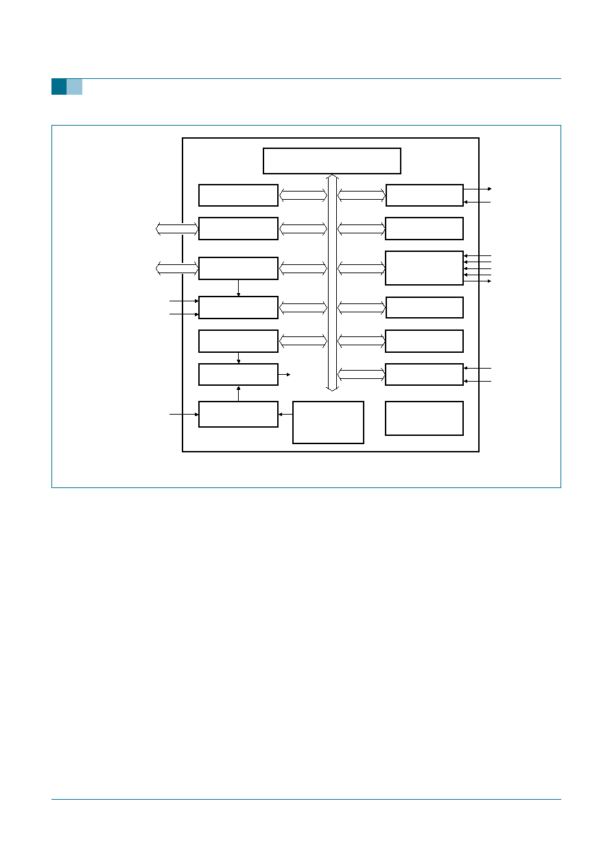
5.
Block diagram
Fig 1.
Block diagram of P89LPC9102.
ACCELERATED 2-CLOCK 80C51 CPU
1 kB
FLASH
PORT 1
CONFIGURABLE I/Os
PORT 0
CONFIGURABLE I/Os
KEYPAD
INTERRUPT
PROGRAMMABLE
OSCILLATOR DIVIDER
CPU clock
CONFIGURABLE
OSCILLATOR
ON-CHIP
RC OSCILLATOR
WITH CLOCK
DOUBLER OPTION
internal
bus
POWER MONITOR
(POWER-ON RESET,
BROWNOUT RESET)
002aaa967
128 BYTE
RAM
ANALOG
COMPARATORS
ADC1/DAC1
P89LPC9102
WATCHDOG TIMER
AND OSCILLATOR
REAL-TIME CLOCK/
SYSTEM TIMER
TIMER 0
TIMER 1
CLKOUT
CLKIN
P1.2, P1.5
P0[1:5], P0.7
KBI1
AD10
AD11
AD12
DAC1
T0
T1
CIN1A
CIN1B
AD13
KBI2
9397 750 14655
� Koninklijke Philips Electronics N.V. 2005. All rights reserved.
Product data sheet
Rev. 02 -- 11 April 2005
5 of 58
Philips Semiconductors
P89LPC9102/9103/9107
8-bit microcontrollers with two-clock accelerated 80C51 core
Fig 2.
Block diagram of P89LPC9103.
ACCELERATED 2-CLOCK 80C51 CPU
1 kB
FLASH
PORT 1
CONFIGURABLE I/Os
PORT 0
CONFIGURABLE I/Os
KEYPAD
INTERRUPT
PROGRAMMABLE
OSCILLATOR DIVIDER
CPU
clock
CONFIGURABLE
OSCILLATOR
internal
bus
POWER MONITOR
(POWER-ON RESET,
BROWNOUT RESET)
002aaa968
UART
ANALOG
COMPARATORS
ADC1/DAC1
P89LPC9103
WATCHDOG TIMER
AND OSCILLATOR
REAL-TIME CLOCK/
SYSTEM TIMER
TIMER 0
TIMER 1
128 BYTE
RAM
CLKIN
ON-CHIP
RC OSCILLATOR
WITH CLOCK
DOUBLER OPTION
P1.0, P1.1, P1.5
P0[1:5]
KBI1
TXD
RXD
CIN1A
CIN1B
KBI2
AD10
AD11
AD12
DAC1
AD13

9397 750 14655
� Koninklijke Philips Electronics N.V. 2005. All rights reserved.
Product data sheet
Rev. 02 -- 11 April 2005
6 of 58
Philips Semiconductors
P89LPC9102/9103/9107
8-bit microcontrollers with two-clock accelerated 80C51 core
6.
Functional diagram
Fig 3.
Block diagram of P89LPC9107.
ACCELERATED 2-CLOCK 80C51 CPU
1 kB
FLASH
PORT 1
CONFIGURABLE I/Os
PORT 0
CONFIGURABLE I/Os
KEYPAD
INTERRUPT
PROGRAMMABLE
OSCILLATOR DIVIDER
CPU
clock
CONFIGURABLE
OSCILLATOR
internal bus
POWER MONITOR
(POWER-ON RESET,
BROWNOUT RESET)
002aab100
UART
ANALOG
COMPARATORS
ADC1/DAC1
P89LPC9107
WATCHDOG TIMER
AND OSCILLATOR
REAL-TIME CLOCK/
SYSTEM TIMER
TIMER 0
TIMER 1
128 BYTE
RAM
CLKIN
CLKOUT
ON-CHIP
RC OSCILLATOR
WITH CLOCK
DOUBLER OPTION
P1[0:2], P1.5
P0[1:5], P0.7
KBI1
AD10
TXD
RXD
AD11
AD12
DAC1
CIN1A
CIN1B
T0
T1
AD13
KBI2
Fig 4.
Functional diagram of P89LPC9102.
V
DD
V
SS
PORT 0
T0
RST
002aaa971
CIN1A
CMPREF
CIN1B
AD13
CLKIN
AD11
AD12
AD10
CLKOUT
DAC1
KBI2
KBI1
T1
PORT 1
P89LPC9102
9397 750 14655
� Koninklijke Philips Electronics N.V. 2005. All rights reserved.
Product data sheet
Rev. 02 -- 11 April 2005
7 of 58
Philips Semiconductors
P89LPC9102/9103/9107
8-bit microcontrollers with two-clock accelerated 80C51 core
Fig 5.
Functional diagram of P89LPC9103.
Fig 6.
Functional diagram of P89LPC9107.
V
DD
V
SS
PORT 0
RXD
RST
002aaa972
CIN1A
CMPREF
CIN1B
AD13
CLKIN
AD11
AD12
AD10
DAC1
KBI2
KBI1
PORT 1
TXD
P89LPC9103
V
DD
V
SS
PORT 0
RXD
RST
002aab084
CIN1A
CMPREF
CIN1B
AD13
CLKIN
AD11
AD12
AD10
DAC1
KBI2
KBI1
CLKOUT
T1
PORT 1
TXD
T0
P89LPC9107
9397 750 14655
� Koninklijke Philips Electronics N.V. 2005. All rights reserved.
Product data sheet
Rev. 02 -- 11 April 2005
8 of 58
Philips Semiconductors
P89LPC9102/9103/9107
8-bit microcontrollers with two-clock accelerated 80C51 core
7.
Pinning information
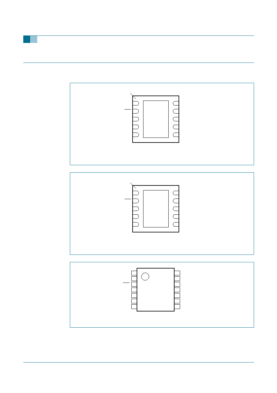
7.1 Pinning
Fig 7.
P89LPC9102 pinning (HVSON10).
Fig 8.
P89LPC9103 pinning (HVSON10).
Fig 9.
P89LPC9107 pinning (TSSOP14).
002aaa969
LPC9102
P0.7/T1/CLKOUT
P1.2/T0
V
DD
V
SS
P0.5/CMPREF/CLKIN
P0.4/CIN1A/AD13/DAC1
P0.2/KBI2/AD11
P0.3/CIN1B/AD12
Transparent top view
5
6
4
7
3
8
2
9
1
10
terminal 1
index area
P1.5/RST
P0.1/KBI1/AD10
002aaa970
LPC9103
P1.1/RXD
P0.1/KBI1/AD10
P1.0/TXD
V
DD
V
SS
P0.5/CMPREF/CLKIN
P1.5/RST
P0.4/CIN1A/AD13/DAC1
P0.2/KBI2/AD11
P0.3/CIN1B/AD12
Transparent top view
5
6
4
7
3
8
2
9
1
10
terminal 1
index area
LPC9107
P0.2/KBI2/AD11
P0.3/CIN1B/AD12
n.c.
n.c.
P1.5/RST
P0.4/CIN1A/AD13/DAC1
V
SS
P0.5/CMPREF/CLKIN
P0.1/KBI1/AD10
V
DD
P1.0/TXD
P1.1/RXD
P1.2/T0
P0.7/T1/CLKOUT
002aab083
1
2
3
4
5
6
7
8
10
9
12
11
14
13

9397 750 14655
� Koninklijke Philips Electronics N.V. 2005. All rights reserved.
Product data sheet
Rev. 02 -- 11 April 2005
9 of 58
Philips Semiconductors
P89LPC9102/9103/9107
8-bit microcontrollers with two-clock accelerated 80C51 core
7.2 Pin description
Table 4:
P89LPC9102 pin description
Symbol
Pin
Type
Description
P0.1 to P0.5,
P0.7
I/O
Port 0: Port 0 is an I/O port with a user-configurable output type. During reset Port 0
latches are configured in the input-only mode with the internal pull-up disabled. The
operation of Port 0 pins as inputs and outputs depends upon the port configuration
selected. Each port pin is configured independently. Refer to
Section 8.12.1 "Port
configurations"
and
Table 12 "Static characteristics"
for details.
The Keypad Interrupt feature operates with Port 0 pins.
All pins have Schmitt triggered inputs.
Port 0 also provides various special functions as described below:
P0.1/KBI1/
AD10
4
I/O
P0.1 -- Port 0 bit 1.
I
KBI1 -- Keyboard input 1.
I
AD10 -- ADC1 channel 0 analog input.
P0.2/KBI2/
AD11
1
I/O
P0.2 -- Port 0 bit 2.
I
KBI2 -- Keyboard input 2.
I
AD11 -- ADC1 channel 1 analog input.
P0.3/CIN1B/
AD12
10
I/O
P0.3 -- Port 0 bit 3.
I
CIN1B -- Comparator 1 positive input.
I
AD12 -- ADC1 channel 2 analog input.
P0.4/CIN1A/
AD13/DAC1
9
I/O
P0.4 -- Port 0 bit 4.
I
CIN1A -- Comparator 1 positive input.
I
AD13 -- ADC1 channel 3 analog input.
O
DAC1 -- Digital to analog converter output.
P0.5/CMPRE
F/CLKIN
8
I/O
P0.5 -- Port 0 bit 5.
I
CMPREF -- Comparator reference (negative) input.
I
CLKIN -- External clock input.
P0.7/T1/
CLKOUT
6
I/O
P0.7 -- Port 0 bit 7.
I/O
T1 -- Timer/counter 1 external count input or overflow/PWM output.
I
CLKOUT -- Clock output.
P1.2, P1.5
I/O
Port 1: Port 1 is an I/O port with a user-configurable output type. During reset Port 1
latches are configured in the input-only mode with the internal pull-up disabled. The
operation of the configurable Port 1 pins as inputs and outputs depends upon the
port configuration selected. Each of the configurable port pins are programmed
independently. Refer to
Section 8.12.1 "Port configurations"
and
Table 12 "Static
characteristics"
for details. P1.5 is input-only.
All pins have Schmitt triggered inputs.
Port 1 also provides various special functions as described below:
P1.2/T0
5
I/O
P1.2 -- Port 1 bit 2.
I/O
T0 -- Timer/counter 0 external count input or overflow/PWM output.

9397 750 14655
� Koninklijke Philips Electronics N.V. 2005. All rights reserved.
Product data sheet
Rev. 02 -- 11 April 2005
10 of 58
Philips Semiconductors
P89LPC9102/9103/9107
8-bit microcontrollers with two-clock accelerated 80C51 core
P1.5/RST
2
I
P1.5 -- Port 1 bit 5 (input-only).
I
RST -- External Reset input during power-on or if selected via User Configuration
Register 1 (UCFG1). When functioning as a reset input a LOW on this pin resets the
microcontroller, causing I/O ports and peripherals to take on their default states, and
the processor begins execution at address 0. When using an oscillator frequency
above 12 MHz, the reset input function of P1.5 must be enabled. An external
circuit is required to hold the device in reset at power-up until V
DD
has reached
its specified level. When system power is removed V
DD
will fall below the
minimum specified operating voltage. When using an oscillator frequency
above 12 MHz, in some applications, an external brownout detect circuit may
be required to hold the device in reset when V
DD
falls below the minimum
specified operating voltage.
V
SS
3
I
Ground: 0 V reference.
V
DD
7
I
Power supply: This is the power supply voltage for normal operation as well as Idle
mode and Power-down mode.
Table 4:
P89LPC9102 pin description
...continued
Symbol
Pin
Type
Description

9397 750 14655
� Koninklijke Philips Electronics N.V. 2005. All rights reserved.
Product data sheet
Rev. 02 -- 11 April 2005
11 of 58
Philips Semiconductors
P89LPC9102/9103/9107
8-bit microcontrollers with two-clock accelerated 80C51 core
Table 5:
P89LPC9103 pin description
Symbol
Pin
Type
Description
P0.1 to P0.5
I/O
Port 0: Port 0 is an I/O port with a user-configurable output type. During reset Port 0
latches are configured in the input-only mode with the internal pull-up disabled. The
operation of Port 0 pins as inputs and outputs depends upon the port configuration
selected. Each port pin is configured independently. Refer to
Section 8.12.1 "Port
configurations"
and
Table 12 "Static characteristics"
for details.
The Keypad Interrupt feature operates with Port 0 pins.
All pins have Schmitt triggered inputs.
Port 0 also provides various special functions as described below:
P0.1/KBI1/
AD10
4
I/O
P0.1 -- Port 0 bit 1.
I
KBI1 -- Keyboard input 1.
I
AD10 -- ADC1 channel 0 analog input.
P0.2/KBI2/
AD11
1
I/O
P0.2 -- Port 0 bit 2.
I
KBI2 -- Keyboard input 2.
I
AD11 -- ADC1 channel 1 analog input.
P0.3/CIN1B/
AD12
10
I/O
P0.3 -- Port 0 bit 3.
I
CIN1B -- Comparator 1 positive input.
I
AD12 -- ADC1 channel 2 analog input.
P0.4/CIN1A/
AD13/DAC1
9
I/O
P0.4 -- Port 0 bit 4.
I
CIN1A -- Comparator 1 positive input.
I
AD13 -- ADC1 channel 3 analog input.
O
DAC1 -- Digital to analog converter output.
P0.5/CMPREF/
CLKIN
6
I/O
P0.5 -- Port 0 bit 5.
I
CMPREF -- Comparator reference (negative) input.
I
CLKIN -- External clock input.
P1.0 to P1.5
I/O
Port 1: Port 1 is an I/O port with a user-configurable output type. During reset Port 1
latches are configured in the input-only mode with the internal pull-up disabled. The
operation of the configurable Port 1 pins as inputs and outputs depends upon the port
configuration selected. Each of the configurable port pins are programmed
independently. Refer to
Section 8.12.1 "Port configurations"
and
Table 12 "Static
characteristics"
for details. P1.5 is input-only.
All pins have Schmitt triggered inputs.
Port 1 also provides various special functions as described below:
P1.0/TXD
5
I/O
P1.0 -- Port 1 bit 0.
O
TXD -- Serial port transmitter data.
P1.1/RXD
6
I/O
P1.1 -- Port 1 bit 1.
I
RXD -- Serial port receiver data.

9397 750 14655
� Koninklijke Philips Electronics N.V. 2005. All rights reserved.
Product data sheet
Rev. 02 -- 11 April 2005
12 of 58
Philips Semiconductors
P89LPC9102/9103/9107
8-bit microcontrollers with two-clock accelerated 80C51 core
P1.5/RST
2
I
P1.5 -- Port 1 bit 5 (input-only).
I
RST -- External Reset input during Power-on or if selected via UCFG1. When
functioning as a reset input a LOW on this pin resets the microcontroller, causing I/O
ports and peripherals to take on their default states, and the processor begins
execution at address 0. When using an oscillator frequency above 12 MHz, the
reset input function of P1.5 must be enabled. An external circuit is required to
hold the device in reset at power-up until V
DD
has reached its specified level.
When system power is removed V
DD
will fall below the minimum specified
operating voltage. When using an oscillator frequency above 12 MHz, in some
applications, an external brownout detect circuit may be required to hold the
device in reset when V
DD
falls below the minimum specified operating voltage.
V
SS
3
I
Ground: 0 V reference.
V
DD
7
I
Power supply: This is the power supply voltage for normal operation as well as Idle
mode and Power-down mode.
Table 5:
P89LPC9103 pin description
...continued
Symbol
Pin
Type
Description
Table 6:
P89LPC9107 pin description
Symbol
Pin
Type
Description
P0.1 to P0.5,
P0.7
I/O
Port 0: Port 0 is an I/O port with a user-configurable output type. During reset Port 0
latches are configured in the input-only mode with the internal pull-up disabled. The
operation of Port 0 pins as inputs and outputs depends upon the port configuration
selected. Each port pin is configured independently. Refer to
Section 8.12.1 "Port
configurations"
and
Table 12 "Static characteristics"
for details.
The Keypad Interrupt feature operates with Port 0 pins.
All pins have Schmitt triggered inputs.
Port 0 also provides various special functions as described below:
P0.1/KBI1/
AD10
5
I/O
P0.1 -- Port 0 bit 1.
I
KBI1 -- Keyboard input 1.
I
AD10 -- ADC1 channel 0 analog input.
P0.2/KBI2/
AD11
1
I/O
P0.2 -- Port 0 bit 2.
I
KBI2 -- Keyboard input 2.
I
AD11 -- ADC1 channel 1 analog input.
P0.3/CIN1B/
AD12
14
I/O
P0.3 -- Port 0 bit 3.
I
CIN1B -- Comparator 1 positive input.
I
AD12 -- ADC1 channel 2 analog input.
P0.4/CIN1A/
AD13/DAC1
12
I/O
P0.4 -- Port 0 bit 4.
I
CIN1A -- Comparator 1 positive input.
I
AD13 -- ADC1 channel 3 analog input.
O
DAC1 -- Digital to analog converter output.
P0.5/CMPREF/
CLKIN
11
I/O
P0.5 -- Port 0 bit 5.
I
CMPREF -- Comparator reference (negative) input.
I
CLKIN -- External clock input.
P0.7/T1/
CLKOUT
8
I/O
P0.7 -- Port 0 bit 7.
I/O
T1 -- Timer/counter 1 external count input or overflow/PWM output.
I
CLKOUT -- Clock output.

9397 750 14655
� Koninklijke Philips Electronics N.V. 2005. All rights reserved.
Product data sheet
Rev. 02 -- 11 April 2005
13 of 58
Philips Semiconductors
P89LPC9102/9103/9107
8-bit microcontrollers with two-clock accelerated 80C51 core
P1.0 to P1.2,
P1.5
I/O
Port 1: Port 1 is an I/O port with a user-configurable output type. During reset Port 1
latches are configured in the input-only mode with the internal pull-up disabled. The
operation of the configurable Port 1 pins as inputs and outputs depends upon the port
configuration selected. Each of the configurable port pins are programmed
independently. Refer to
Section 8.12.1 "Port configurations"
and
Table 12 "Static
characteristics"
for details. P1.5 is input-only.
All pins have Schmitt triggered inputs.
Port 1 also provides various special functions as described below:
P1.0/TXD
6
I/O
P1.0 -- Port 1 bit 0.
O
TXD -- Serial port transmitter data.
P1.1/RXD
9
I/O
P1.1 -- Port 1 bit 1.
I
RXD -- Serial port receiver data.
P1.2/T0
7
I/O
P1.2 -- Port 1 bit 2.
I/O
T0 -- Timer/counter 0 external count input or overflow/PWM output.
P1.5/RST
3
I
P1.5 -- Port 1 bit 5 (input-only).
I
RST -- External Reset input during Power-on or if selected via UCFG1. When
functioning as a reset input a LOW on this pin resets the microcontroller, causing I/O
ports and peripherals to take on their default states, and the processor begins
execution at address 0. When using an oscillator frequency above 12 MHz, the
reset input function of P1.5 must be enabled. An external circuit is required to
hold the device in reset at power-up until V
DD
has reached its specified level.
When system power is removed V
DD
will fall below the minimum specified
operating voltage. When using an oscillator frequency above 12 MHz, in some
applications, an external brownout detect circuit may be required to hold the
device in reset when V
DD
falls below the minimum specified operating voltage.
V
SS
4
I
Ground: 0 V reference.
V
DD
10
I
Power supply: This is the power supply voltage for normal operation as well as Idle
mode and Power-down mode.
Table 6:
P89LPC9107 pin description
...continued
Symbol
Pin
Type
Description

9397 750 14655
� Koninklijke Philips Electronics N.V. 2005. All rights reserved.
Product data sheet
Rev. 02 -- 11 April 2005
14 of 58
Philips Semiconductors
P89LPC9102/9103/9107
8-bit microcontrollers with two-clock accelerated 80C51 core
8.
Functional description
Remark: Please refer to the
P89LPC9102/9103/9107 User manual for a more detailed
functional description.
8.1 Special function registers
Remark: Special Function Registers (SFRs) accesses are restricted in the following
ways:
�
User must not attempt to access any SFR locations not defined.
�
Accesses to any defined SFR locations must be strictly for the functions for the SFRs.
�
SFR bits labeled `-', `0' or `1' can only be written and read as follows:
� `-' Unless otherwise specified, must be written with `0', but can return any value
when read (even if it was written with `0'). It is a reserved bit and may be used in
future derivatives.
� `0' must be written with `0', and will return a `0' when read.
� `1' must be written with `1', and will return a `1' when read.

xxxxxxxxxxxxxxxxxxxxx xxxxxxxxxxxxxxxxxxxxxxxxxx xxxxxxx x x x xxxxxxxxxxxxxxxxxxxxxxxxxxxxxx xxxxxxxxxxxxxxxxxxx xx xx
xxxxx xxxxxxxxxxxxxxxxxxxxxxxxxxx xxxxxxxxxxxxxxxxxxx xxxxxx xxxxxxxxxxxxxxxxxxxxxxxxxxxxxxxxxxx xxxxxxxxxxxx x x
xxxxxxxxxxxxxxxxxxxxx xxxxxxxxxxxxxxxxxxxxxxxxxxxxxx xxxxx xxxxxxxxxxxxxxxxxxxxxxxxxxxxxxxxxxxxxxxxxxxxxxxxxx xxxxxxxx
xxxxxxxxxxxxxxxxxxxxxxxxx xxxxxxxxxxxxxxxxxxxx xxx
9397 750 14655
� K
oninklijk
e Philips Electronics N.V
. 2005. All r
ights reser
v
ed.
Pr
oduct data sheet
Re
v
.
02 -- 11 April 2005
15 of 58
Philips Semiconductor
s
P89LPC9102/9103/9107
8-bit micr
ocontr
oller
s with tw
o-c
loc
k accelerated 80C51 core
Table 7:
P89LPC9102 special function registers
* indicates SFRs that are bit addressable.
Name
Description
SFR
addr.
Bit functions and addresses
Reset value
MSB
LSB
Hex
Binary
Bit address
E7
E6
E5
E4
E3
E2
E1
E0
ACC*
Accumulator
E0h
00
00000000
ADCON1
A/D control register 1
97h
ENBI1
ENADCI
1
TMM1
-
ADCI1
ENADC1
ADCS11
ADCS10 00
00000000
ADINS
A/D input select
A3h
ADI13
AD12
ADI11
AD10
-
-
-
-
00
00000000
ADMODA
A/D mode register A
C0h
BNDI1
BURST1
SCC1
SCAN1
-
-
-
-
00
00000000
ADMODB
A/D mode register B
A1h
CLK2
CLK1
CLK0
-
ENDAC1
-
BSA1
-
00
000x0000
AD1BH
A/D_1 boundary high register
C4h
FF
11111111
AD1BL
A/D_1 boundary low register
BCh
00
00000000
AD1DAT0
A/D_1 data register 0
D5h
00
00000000
AD1DAT1
A/D_1 data register 1
D6h
00
00000000
AD1DAT2
A/D_1 data register 2
D7h
00
00000000
AD1DAT3
A/D_1 data register 3
F5h
00
00000000
AUXR1
Auxiliary function register
A2h
CLKLP
EBRR
ENT1
ENT0
SRST
0
-
DPS
00
[1]
000000x0
Bit address
F7
F6
F5
F4
F3
F2
F1
F0
B*
B register
F0h
00
00000000
CMP1
Comparator 1 control register
ACh
-
-
CE1
CP1
CN1
-
CO1
CMF1
00
xx000000
DIVM
CPU clock divide-by-M
control
95h
00
00000000
DPTR
Data pointer (2 bytes)
DPH
Data pointer high
83h
00
00000000
DPL
Data pointer low
82h
00
00000000
FMADRH
Program Flash address high
E7h
00
00000000
FMADRL
Program Flash address low
E6h
00
00000000
FMCON
Program Flash Control
(Read)
E4h
BUSY
-
-
-
HVA
HVE
SV
OI
70
01110000
Program Flash Control
(Write)
FMCMD.
7
FMCMD.
6
FMCMD.
5
FMCMD.
4
FMCMD.
3
FMCMD.
2
FMCMD.
1
FMCMD.
0
FMDATA
Program Flash data
E5h
00
00000000
IEN0*
Interrupt enable 0
A8h
EA
EWDRT
EBO
-
ET1
-
ET0
-
00
00000000

xxxxxxxxxxxxxxxxxxxxx xxxxxxxxxxxxxxxxxxxxxxxxxx xxxxxxx x x x xxxxxxxxxxxxxxxxxxxxxxxxxxxxxx xxxxxxxxxxxxxxxxxxx xx xx
xxxxx xxxxxxxxxxxxxxxxxxxxxxxxxxx xxxxxxxxxxxxxxxxxxx xxxxxx xxxxxxxxxxxxxxxxxxxxxxxxxxxxxxxxxxx xxxxxxxxxxxx x x
xxxxxxxxxxxxxxxxxxxxx xxxxxxxxxxxxxxxxxxxxxxxxxxxxxx xxxxx xxxxxxxxxxxxxxxxxxxxxxxxxxxxxxxxxxxxxxxxxxxxxxxxxx xxxxxxxx
xxxxxxxxxxxxxxxxxxxxxxxxx xxxxxxxxxxxxxxxxxxxx xxx
9397 750 14655
� K
oninklijk
e Philips Electronics N.V
. 2005. All r
ights reser
v
ed.
Pr
oduct data sheet
Re
v
.
02 -- 11 April 2005
16 of 58
Philips Semiconductor
s
P89LPC9102/9103/9107
8-bit micr
ocontr
oller
s with tw
o-c
loc
k accelerated 80C51 core
Bit address
EF
EE
ED
EC
EB
EA
E9
E8
IEN1*
Interrupt enable 1
E8h
EAD
-
-
-
-
EC
EKBI
-
00
[1]
00x00000
Bit address
BF
BE
BD
BC
BB
BA
B9
B8
IP0*
Interrupt priority 0
B8h
-
PWDRT
PBO
-
PT1
-
PT0
-
00
[1]
x0000000
IP0H
Interrupt priority 0 high
B7h
-
PWDRT
H
PBOH
-
PT1H
-
PT0H
-
00
[1]
x0000000
Bit address
FF
FE
FD
FC
FB
FA
F9
F8
IP1*
Interrupt priority 1
F8h
PAD
-
-
-
-
PC
PKBI
-
00
[1]
00x00000
IP1H
Interrupt priority 1 high
F7h
PADH
-
-
-
-
PCH
PKBIH
-
00
[1]
00x00000
KBCON
Keypad control register
94h
-
-
-
-
-
-
PATN
_SEL
KBIF
00
[1]
xxxxxx00
KBMASK
Keypad interrupt mask
register
86h
-
-
-
KBMASK
.2
KBMASK
.1
-
-
00
xxxxx00x
KBPATN
Keypad pattern register
93h
-
-
-
-
KBPATN.
2
KBPATN.
1
-
-
FF
xxxxx11x
Bit address
87
86
85
84
83
82
81
80
P0*
Port 0
80h
CLKOUT/
T1
-
CMPREF
/CLKIN
CIN1A
CIN1B
CIN2A
/KBI2
KBI1
-
[2]
Bit address
97
96
95
94
93
92
91
90
P1*
Port 1
90h
-
-
RST
-
-
T0
-
-
P0M1
Port 0 output mode 1
84h
(P0M1.7)
-
(P0M1.5) (P0M1.4) (P0M1.3) (P0M1.2) (P0M1.1)
-
FF
11111111
P0M2
Port 0 output mode 2
85h
(P0M2.7)
-
(P0M2.5) (P0M2.4) (P0M2.3) (P0M2.2) (P0M2.1)
-
00
00000000
P1M1
Port 1 output mode 1
91h
-
-
-
-
-
(P1M1.2)
-
-
FF
[2]
11111111
P1M2
Port 1 output mode 2
92h
-
-
-
-
-
(P1M2.2)
-
-
00
[2]
00000000
PCON
Power control register
87h
-
-
BOPD
BOI
GF1
GF0
PMOD1
PMOD0
00
00000000
PCONA
Power control register A
B5h
RTCPD
VCPD
ADPD
-
-
00
[1]
00000000
PCONB
reserved for Power control
register B
B6h
-
-
-
-
-
-
-
-
00
[1]
xxxxxxxx
Bit address
D7
D6
D5
D4
D3
D2
D1
D0
PSW*
Program status word
D0h
CY
AC
F0
RS1
RS0
OV
F1
P
00
00000000
PT0AD
Port 0 digital input disable
F6h
-
-
PT0AD.5
PT0AD.4
PT0AD.3
PT0AD.2
PT0AD.1
-
00
xx00000x
Table 7:
P89LPC9102 special function registers
...continued
* indicates SFRs that are bit addressable.
Name
Description
SFR
addr.
Bit functions and addresses
Reset value
MSB
LSB
Hex
Binary

xxxxxxxxxxxxxxxxxxxxx xxxxxxxxxxxxxxxxxxxxxxxxxx xxxxxxx x x x xxxxxxxxxxxxxxxxxxxxxxxxxxxxxx xxxxxxxxxxxxxxxxxxx xx xx
xxxxx xxxxxxxxxxxxxxxxxxxxxxxxxxx xxxxxxxxxxxxxxxxxxx xxxxxx xxxxxxxxxxxxxxxxxxxxxxxxxxxxxxxxxxx xxxxxxxxxxxx x x
xxxxxxxxxxxxxxxxxxxxx xxxxxxxxxxxxxxxxxxxxxxxxxxxxxx xxxxx xxxxxxxxxxxxxxxxxxxxxxxxxxxxxxxxxxxxxxxxxxxxxxxxxx xxxxxxxx
xxxxxxxxxxxxxxxxxxxxxxxxx xxxxxxxxxxxxxxxxxxxx xxx
9397 750 14655
� K
oninklijk
e Philips Electronics N.V
. 2005. All r
ights reser
v
ed.
Pr
oduct data sheet
Re
v
.
02 -- 11 April 2005
17 of 58
Philips Semiconductor
s
P89LPC9102/9103/9107
8-bit micr
ocontr
oller
s with tw
o-c
loc
k accelerated 80C51 core
[1]
Unimplemented bits in SFRs (labeled '-') are X (unknown) at all times. Unless otherwise specified, ones should not be written to these bits since they may be used for other
purposes in future derivatives. The reset values shown for these bits are logic 0s although they are unknown when read.
[2]
All ports are in input-only (high-impedance) state after power-up.
[3]
The RSTSRC register reflects the cause of the P89LPC9102/9103/9107 reset. Upon a power-up reset, all reset source flags are cleared except POF and BOF; the power-on reset
value is xx110000.
[4]
The only reset source that affects these SFRs is power-on reset.
[5]
On power-on reset, the TRIM SFR is initialized with a factory preprogrammed value. Other resets will not cause initialization of the TRIM register.
[6]
After reset, the value is 111001x1, i.e., PRE2 to PRE0 are all logic 1s, WDRUN = 1 and WDCLK = 1. WDTOF bit is logic 1 after watchdog timer reset and is logic 0 after power-on
reset. Other resets will not affect WDTOF.
RSTSRC
Reset source register
DFh
-
-
BOF
POF
-
R_WD
R_SF
R_EX
[3]
RTCCON
Real-time clock control
D1h
RTCF
RTCS1
RTCS0
-
-
-
ERTC
RTCEN
60
[2]
[4]
011xxx00
RTCH
Real-time clock register high
D2h
00
[4]
00000000
RTCL
Real-time clock register low
D3h
00
[4]
00000000
SP
Stack pointer
81h
07
00000111
TAMOD
Timer 0 and 1 auxiliary mode
8Fh
-
-
-
T1M2
-
-
-
T0M2
00
xxx0xxx0
Bit address
8F
8E
8D
8C
8B
8A
89
88
TCON*
Timer 0 and 1 control
88h
TF1
TR1
TF0
TR0
-
-
-
-
00
00000000
TH0
Timer 0 high
8Ch
00
00000000
TH1
Timer 1 high
8Dh
00
00000000
TL0
Timer 0 low
8Ah
00
00000000
TL1
Timer 1 low
8Bh
00
00000000
TMOD
Timer 0 and 1 mode
89h
-
-
T1M1
T1M0
-
-
T0M1
T0M0
00
00000000
TRIM
Internal oscillator trim register
96h
RCCLK
ENCLK
TRIM.5
TRIM.4
TRIM.3
TRIM.2
TRIM.1
TRIM.0
[5] [4]
WDCON
Watchdog control register
A7h
PRE2
PRE1
PRE0
-
-
WDRUN
WDTOF
WDCLK
[6] [4]
WDL
Watchdog load
C1h
FF
11111111
WFEED1
Watchdog feed 1
C2h
WFEED2
Watchdog feed 2
C3h
Table 7:
P89LPC9102 special function registers
...continued
* indicates SFRs that are bit addressable.
Name
Description
SFR
addr.
Bit functions and addresses
Reset value
MSB
LSB
Hex
Binary

xxxxxxxxxxxxxxxxxxxxx xxxxxxxxxxxxxxxxxxxxxxxxxx xxxxxxx x x x xxxxxxxxxxxxxxxxxxxxxxxxxxxxxx xxxxxxxxxxxxxxxxxxx xx xx
xxxxx xxxxxxxxxxxxxxxxxxxxxxxxxxx xxxxxxxxxxxxxxxxxxx xxxxxx xxxxxxxxxxxxxxxxxxxxxxxxxxxxxxxxxxx xxxxxxxxxxxx x x
xxxxxxxxxxxxxxxxxxxxx xxxxxxxxxxxxxxxxxxxxxxxxxxxxxx xxxxx xxxxxxxxxxxxxxxxxxxxxxxxxxxxxxxxxxxxxxxxxxxxxxxxxx xxxxxxxx
xxxxxxxxxxxxxxxxxxxxxxxxx xxxxxxxxxxxxxxxxxxxx xxx
9397 750 14655
� K
oninklijk
e Philips Electronics N.V
. 2005. All r
ights reser
v
ed.
Pr
oduct data sheet
Re
v
.
02 -- 11 April 2005
18 of 58
Philips Semiconductor
s
P89LPC9102/9103/9107
8-bit micr
ocontr
oller
s with tw
o-c
loc
k accelerated 80C51 core
Table 8:
P89LPC9103 special function registers
* indicates SFRs that are bit addressable.
Name
Description
SFR
addr.
Bit functions and addresses
Reset value
MSB
LSB
Hex
Binary
Bit address
E7
E6
E5
E4
E3
E2
E1
E0
ACC*
Accumulator
E0h
00
00000000
ADCON1
A/D control register 1
97h
ENBI1
ENADCI
1
TMM1
-
ADCI1
ENADC1
ADCS11
ADCS10 00
00000000
ADINS
A/D input select
A3h
ADI13
AD12
ADI11
AD10
-
-
-
-
00
00000000
ADMODA
A/D mode register A
C0h
BNDI1
BURST1
SCC1
SCAN1
-
-
-
-
00
00000000
ADMODB
A/D mode register B
A1h
CLK2
CLK1
CLK0
-
ENDAC1
-
BSA1
-
00
000x0000
AD1BH
A/D_1 boundary high register
C4h
FF
11111111
AD1BL
A/D_1 boundary low register
BCh
00
00000000
AD1DAT0
A/D_1 data register 0
D5h
00
00000000
AD1DAT1
A/D_1 data register 1
D6h
00
00000000
AD1DAT2
A/D_1 data register 2
D7h
00
00000000
AD1DAT3
A/D_1 data register 3
F5h
00
00000000
AUXR1
Auxiliary function register
A2h
CLKLP
EBRR
-
-
SRST
0
-
DPS
00
[1]
000000x0
Bit address
F7
F6
F5
F4
F3
F2
F1
F0
B*
B register
F0h
00
00000000
BRGR0
[2]
Baud rate generator rate low
BEh
00
00000000
BRGR1
[2]
Baud rate generator rate high
BFh
00
00000000
BRGCON
Baud rate generator control
BDh
-
-
-
-
-
-
SBRGS
BRGEN
00
[2]
xxxxxx00
CMP1
Comparator 1 control register
ACh
-
-
CE1
CP1
CN1
-
CO1
CMF1
00
[3]
xx000000
DIVM
CPU clock divide-by-M
control
95h
00
00000000
DPTR
Data pointer (2 bytes)
DPH
Data pointer high
83h
00
00000000
DPL
Data pointer low
82h
00
00000000
FMADRH
Program Flash address high
E7h
00
00000000
FMADRL
Program Flash address low
E6h
00
00000000

xxxxxxxxxxxxxxxxxxxxx xxxxxxxxxxxxxxxxxxxxxxxxxx xxxxxxx x x x xxxxxxxxxxxxxxxxxxxxxxxxxxxxxx xxxxxxxxxxxxxxxxxxx xx xx
xxxxx xxxxxxxxxxxxxxxxxxxxxxxxxxx xxxxxxxxxxxxxxxxxxx xxxxxx xxxxxxxxxxxxxxxxxxxxxxxxxxxxxxxxxxx xxxxxxxxxxxx x x
xxxxxxxxxxxxxxxxxxxxx xxxxxxxxxxxxxxxxxxxxxxxxxxxxxx xxxxx xxxxxxxxxxxxxxxxxxxxxxxxxxxxxxxxxxxxxxxxxxxxxxxxxx xxxxxxxx
xxxxxxxxxxxxxxxxxxxxxxxxx xxxxxxxxxxxxxxxxxxxx xxx
9397 750 14655
� K
oninklijk
e Philips Electronics N.V
. 2005. All r
ights reser
v
ed.
Pr
oduct data sheet
Re
v
.
02 -- 11 April 2005
19 of 58
Philips Semiconductor
s
P89LPC9102/9103/9107
8-bit micr
ocontr
oller
s with tw
o-c
loc
k accelerated 80C51 core
FMCON
Program Flash Control
(Read)
E4h
BUSY
-
-
-
HVA
HVE
SV
OI
70
01110000
Program Flash Control
(Write)
FMCMD.
7
FMCMD.
6
FMCMD.
5
FMCMD.
4
FMCMD.
3
FMCMD.
2
FMCMD.
1
FMCMD.
0
FMDATA
Program Flash data
E5h
00
00000000
IEN0*
Interrupt enable 0
A8h
EA
EWDRT
EBO
ES/ESR
ET1
-
ET0
-
00
00000000
Bit address
EF
EE
ED
EC
EB
EA
E9
E8
IEN1*
Interrupt enable 1
E8h
EAD
EST
-
-
-
EC
EKBI
-
00
[1]
00x00000
Bit address
BF
BE
BD
BC
BB
BA
B9
B8
IP0*
Interrupt priority 0
B8h
-
PWDRT
PBO
PS/PSR
PT1
-
PT0
-
00
[1]
x0000000
IP0H
Interrupt priority 0 high
B7h
-
PWDRT
H
PBOH
PSH
/PSRH
PT1H
-
PT0H
-
00
[1]
x0000000
Bit address
FF
FE
FD
FC
FB
FA
F9
F8
IP1*
Interrupt priority 1
F8h
PAD
PST
-
-
-
PC
PKBI
-
00
[1]
00x00000
IP1H
Interrupt priority 1 high
F7h
PADH
PSTH
-
-
-
PCH
PKBIH
-
00
[1]
00x00000
KBCON
Keypad control register
94h
-
-
-
-
-
-
PATN
_SEL
KBIF
00
[1]
xxxxxx00
KBMASK
Keypad interrupt mask
register
86h
-
-
-
-
KBMASK
.2
KBMASK
.1
-
00
xxxxx00x
KBPATN
Keypad pattern register
93h
-
-
-
-
-
KBPATN.
2
KBPATN.
1
-
FF
xxxxx11x
Bit address
87
86
85
84
83
82
81
80
P0*
Port 0
80h
-
-
CMPREF
/CLKIN
CIN1A
CIN1B
KBI2
KBI1
-
[3]
Bit address
97
96
95
94
93
92
91
90
P1*
Port 1
90h
-
-
RST
-
-
-
RXD
TXD
P0M1
Port 0 output mode 1
84h
-
-
(P0M1.5) (P0M1.4) (P0M1.3) (P0M1.2) (P0M1.1)
-
FF
11111111
P0M2
Port 0 output mode 2
85h
-
-
(P0M2.5) (P0M2.4) (P0M2.3) (P0M2.2) (P0M2.1)
-
00
00000000
P1M1
Port 1 output mode 1
91h
-
-
-
-
-
-
(P1M1.1) (P1M1.0) FF
[3]
11111111
P1M2
Port 1 output mode 2
92h
-
-
-
-
-
-
(P1M2.1) (P1M2.0) 00
[3]
00000000
PCON
Power control register
87h
SMOD1
SMOD0
BOPD
BOI
GF1
GF0
PMOD1
PMOD0
00
00000000
Table 8:
P89LPC9103 special function registers
...continued
* indicates SFRs that are bit addressable.
Name
Description
SFR
addr.
Bit functions and addresses
Reset value
MSB
LSB
Hex
Binary

xxxxxxxxxxxxxxxxxxxxx xxxxxxxxxxxxxxxxxxxxxxxxxx xxxxxxx x x x xxxxxxxxxxxxxxxxxxxxxxxxxxxxxx xxxxxxxxxxxxxxxxxxx xx xx
xxxxx xxxxxxxxxxxxxxxxxxxxxxxxxxx xxxxxxxxxxxxxxxxxxx xxxxxx xxxxxxxxxxxxxxxxxxxxxxxxxxxxxxxxxxx xxxxxxxxxxxx x x
xxxxxxxxxxxxxxxxxxxxx xxxxxxxxxxxxxxxxxxxxxxxxxxxxxx xxxxx xxxxxxxxxxxxxxxxxxxxxxxxxxxxxxxxxxxxxxxxxxxxxxxxxx xxxxxxxx
xxxxxxxxxxxxxxxxxxxxxxxxx xxxxxxxxxxxxxxxxxxxx xxx
9397 750 14655
� K
oninklijk
e Philips Electronics N.V
. 2005. All r
ights reser
v
ed.
Pr
oduct data sheet
Re
v
.
02 -- 11 April 2005
20 of 58
Philips Semiconductor
s
P89LPC9102/9103/9107
8-bit micr
ocontr
oller
s with tw
o-c
loc
k accelerated 80C51 core
PCONA
Power control register A
B5h
RTCPD
VCPD
ADPD
-
SPD
00
[1]
00000000
PCONB
reserved for Power control
register B
B6h
-
-
-
-
-
-
-
-
00
[1]
xxxxxxxx
Bit address
D7
D6
D5
D4
D3
D2
D1
D0
PSW*
Program status word
D0h
CY
AC
F0
RS1
RS0
OV
F1
P
00
00000000
PT0AD
Port 0 digital input disable
F6h
-
-
PT0AD.5
PT0AD.4
PT0AD.3
PT0AD.2
PT0AD.1
-
00
xx00000x
RSTSRC
Reset source register
DFh
-
-
BOF
POF
R_BK
R_WD
R_SF
R_EX
[4]
RTCCON
Real-time clock control
D1h
RTCF
RTCS1
RTCS0
-
-
-
ERTC
RTCEN
60
[3]
[5]
011xxx00
RTCH
Real-time clock register high
D2h
00
[5]
00000000
RTCL
Real-time clock register low
D3h
00
[5]
00000000
SADDR
Serial port address register
A9h
00
00000000
SADEN
Serial port address enable
B9h
00
00000000
SBUF
Serial port data buffer register
99h
xx
xxxxxxxx
Bit address
9F
9E
9D
9C
9B
9A
99
98
SCON*
Serial port control
98h
SM0/FE
SM1
SM2
REN
TB8
RB8
TI
RI
00
00000000
SSTAT
Serial port extended status
register
BAh
DBMOD
INTLO
CIDIS
DBISEL
FE
BR
OE
STINT
00
00000000
SP
Stack pointer
81h
07
00000111
Bit address
8F
8E
8D
8C
8B
8A
89
88
TCON*
Timer 0 and 1 control
88h
TF1
TR1
TF0
TR0
-
-
-
-
00
00000000
TH0
Timer 0 high
8Ch
00
00000000
TH1
Timer 1 high
8Dh
00
00000000
TL0
Timer 0 low
8Ah
00
00000000
TL1
Timer 1 low
8Bh
00
00000000
TMOD
Timer 0 and 1 mode
89h
-
-
T1M1
T1M0
-
-
T0M1
T0M0
00
00000000
TRIM
Internal oscillator trim register
96h
RCCLK
-
TRIM.5
TRIM.4
TRIM.3
TRIM.2
TRIM.1
TRIM.0
[6] [5]
WDCON
Watchdog control register
A7h
PRE2
PRE1
PRE0
-
-
WDRUN
WDTOF
WDCLK
[7] [5]
Table 8:
P89LPC9103 special function registers
...continued
* indicates SFRs that are bit addressable.
Name
Description
SFR
addr.
Bit functions and addresses
Reset value
MSB
LSB
Hex
Binary

xxxxxxxxxxxxxxxxxxxxx xxxxxxxxxxxxxxxxxxxxxxxxxx xxxxxxx x x x xxxxxxxxxxxxxxxxxxxxxxxxxxxxxx xxxxxxxxxxxxxxxxxxx xx xx
xxxxx xxxxxxxxxxxxxxxxxxxxxxxxxxx xxxxxxxxxxxxxxxxxxx xxxxxx xxxxxxxxxxxxxxxxxxxxxxxxxxxxxxxxxxx xxxxxxxxxxxx x x
xxxxxxxxxxxxxxxxxxxxx xxxxxxxxxxxxxxxxxxxxxxxxxxxxxx xxxxx xxxxxxxxxxxxxxxxxxxxxxxxxxxxxxxxxxxxxxxxxxxxxxxxxx xxxxxxxx
xxxxxxxxxxxxxxxxxxxxxxxxx xxxxxxxxxxxxxxxxxxxx xxx
9397 750 14655
� K
oninklijk
e Philips Electronics N.V
. 2005. All r
ights reser
v
ed.
Pr
oduct data sheet
Re
v
.
02 -- 11 April 2005
21 of 58
Philips Semiconductor
s
P89LPC9102/9103/9107
8-bit micr
ocontr
oller
s with tw
o-c
loc
k accelerated 80C51 core
[1]
Unimplemented bits in SFRs (labeled '-') are X (unknown) at all times. Unless otherwise specified, ones should not be written to these bits since they may be used for other
purposes in future derivatives. The reset values shown for these bits are logic 0s although they are unknown when read.
[2]
BRGR1 and BRGR0 must only be written if BRGEN in BRGCON SFR is logic 0. If any are written while BRGEN = 1, the result is unpredictable.
[3]
All ports are in input-only (high-impedance) state after power-up.
[4]
The RSTSRC register reflects the cause of the P89LPC9102/9103/9107 reset. Upon a power-up reset, all reset source flags are cleared except POF and BOF; the power-on reset
value is xx110000.
[5]
The only reset source that affects these SFRs is power-on reset.
[6]
On power-on reset, the TRIM SFR is initialized with a factory preprogrammed value. Other resets will not cause initialization of the TRIM register.
[7]
After reset, the value is 111001x1, i.e., PRE2 to PRE0 are all logic 1s, WDRUN = 1 and WDCLK = 1. WDTOF bit is logic 1 after watchdog timer reset and is logic 0 after power-on
reset. Other resets will not affect WDTOF.
WDL
Watchdog load
C1h
FF
11111111
WFEED1
Watchdog feed 1
C2h
WFEED2
Watchdog feed 2
C3h
Table 8:
P89LPC9103 special function registers
...continued
* indicates SFRs that are bit addressable.
Name
Description
SFR
addr.
Bit functions and addresses
Reset value
MSB
LSB
Hex
Binary

xxxxxxxxxxxxxxxxxxxxx xxxxxxxxxxxxxxxxxxxxxxxxxx xxxxxxx x x x xxxxxxxxxxxxxxxxxxxxxxxxxxxxxx xxxxxxxxxxxxxxxxxxx xx xx
xxxxx xxxxxxxxxxxxxxxxxxxxxxxxxxx xxxxxxxxxxxxxxxxxxx xxxxxx xxxxxxxxxxxxxxxxxxxxxxxxxxxxxxxxxxx xxxxxxxxxxxx x x
xxxxxxxxxxxxxxxxxxxxx xxxxxxxxxxxxxxxxxxxxxxxxxxxxxx xxxxx xxxxxxxxxxxxxxxxxxxxxxxxxxxxxxxxxxxxxxxxxxxxxxxxxx xxxxxxxx
xxxxxxxxxxxxxxxxxxxxxxxxx xxxxxxxxxxxxxxxxxxxx xxx
9397 750 14655
� K
oninklijk
e Philips Electronics N.V
. 2005. All r
ights reser
v
ed.
Pr
oduct data sheet
Re
v
.
02 -- 11 April 2005
22 of 58
Philips Semiconductor
s
P89LPC9102/9103/9107
8-bit micr
ocontr
oller
s with tw
o-c
loc
k accelerated 80C51 core
Table 9:
P89LPC9107 special function registers
* indicates SFRs that are bit addressable.
Name
Description
SFR
addr.
Bit functions and addresses
Reset value
MSB
LSB
Hex
Binary
Bit address
E7
E6
E5
E4
E3
E2
E1
E0
ACC*
Accumulator
E0h
00
00000000
ADCON1
A/D control register 1
97h
ENBI1
ENADCI
1
TMM1
-
ADCI1
ENADC1
ADCS11
ADCS10 00
00000000
ADINS
A/D input select
A3h
ADI13
AD12
ADI11
AD10
-
-
-
-
00
00000000
ADMODA
A/D mode register A
C0h
BNDI1
BURST1
SCC1
SCAN1
-
-
-
-
00
00000000
ADMODB
A/D mode register B
A1h
CLK2
CLK1
CLK0
-
ENDAC1
-
BSA1
-
00
000x0000
AD1BH
A/D_1 boundary high register
C4h
FF
11111111
AD1BL
A/D_1 boundary low register
BCh
00
00000000
AD1DAT0
A/D_1 data register 0
D5h
00
00000000
AD1DAT1
A/D_1 data register 1
D6h
00
00000000
AD1DAT2
A/D_1 data register 2
D7h
00
00000000
AD1DAT3
A/D_1 data register 3
F5h
00
00000000
AUXR1
Auxiliary function register
A2h
CLKLP
EBRR
ENT1
ENT0
SRST
0
-
DPS
00
[1]
000000x0
Bit address
F7
F6
F5
F4
F3
F2
F1
F0
B*
B register
F0h
00
00000000
BRGR0
[2]
Baud rate generator rate low
BEh
00
00000000
BRGR1
[2]
Baud rate generator rate high
BFh
00
00000000
BRGCON
Baud rate generator control
BDh
-
-
-
-
-
-
SBRGS
BRGEN
00
[2]
xxxxxx00
CMP1
Comparator 1 control register
ACh
-
-
CE1
CP1
CN1
-
CO1
CMF1
00
[3]
xx000000
DIVM
CPU clock divide-by-M
control
95h
00
00000000
DPTR
Data pointer (2 bytes)
DPH
Data pointer high
83h
00
00000000
DPL
Data pointer low
82h
00
00000000
FMADRH
Program Flash address high
E7h
00
00000000
FMADRL
Program Flash address low
E6h
00
00000000

xxxxxxxxxxxxxxxxxxxxx xxxxxxxxxxxxxxxxxxxxxxxxxx xxxxxxx x x x xxxxxxxxxxxxxxxxxxxxxxxxxxxxxx xxxxxxxxxxxxxxxxxxx xx xx
xxxxx xxxxxxxxxxxxxxxxxxxxxxxxxxx xxxxxxxxxxxxxxxxxxx xxxxxx xxxxxxxxxxxxxxxxxxxxxxxxxxxxxxxxxxx xxxxxxxxxxxx x x
xxxxxxxxxxxxxxxxxxxxx xxxxxxxxxxxxxxxxxxxxxxxxxxxxxx xxxxx xxxxxxxxxxxxxxxxxxxxxxxxxxxxxxxxxxxxxxxxxxxxxxxxxx xxxxxxxx
xxxxxxxxxxxxxxxxxxxxxxxxx xxxxxxxxxxxxxxxxxxxx xxx
9397 750 14655
� K
oninklijk
e Philips Electronics N.V
. 2005. All r
ights reser
v
ed.
Pr
oduct data sheet
Re
v
.
02 -- 11 April 2005
23 of 58
Philips Semiconductor
s
P89LPC9102/9103/9107
8-bit micr
ocontr
oller
s with tw
o-c
loc
k accelerated 80C51 core
FMCON
Program Flash Control
(Read)
E4h
BUSY
-
-
-
HVA
HVE
SV
OI
70
01110000
Program Flash Control
(Write)
FMCMD.
7
FMCMD.
6
FMCMD.
5
FMCMD.
4
FMCMD.
3
FMCMD.
2
FMCMD.
1
FMCMD.
0
FMDATA
Program Flash data
E5h
00
00000000
IEN0*
Interrupt enable 0
A8h
EA
EWDRT
EBO
ES/ESR
ET1
-
ET0
-
00
00000000
Bit address
EF
EE
ED
EC
EB
EA
E9
E8
IEN1*
Interrupt enable 1
E8h
EAD
EST
-
-
-
EC
EKBI
-
00
[1]
00x00000
Bit address
BF
BE
BD
BC
BB
BA
B9
B8
IP0*
Interrupt priority 0
B8h
-
PWDRT
PBO
PS/PSR
PT1
-
PT0
-
00
[1]
x0000000
IP0H
Interrupt priority 0 high
B7h
-
PWDRT
H
PBOH
PSH
/PSRH
PT1H
-
PT0H
-
00
[1]
x0000000
Bit address
FF
FE
FD
FC
FB
FA
F9
F8
IP1*
Interrupt priority 1
F8h
PAD
PST
-
-
-
PC
PKBI
-
00
[1]
00x00000
IP1H
Interrupt priority 1 high
F7h
PADH
PSTH
-
-
-
PCH
PKBIH
-
00
[1]
00x00000
KBCON
Keypad control register
94h
-
-
-
-
-
-
PATN
_SEL
KBIF
00
[1]
xxxxxx00
KBMASK
Keypad interrupt mask
register
86h
-
-
-
-
KBMASK
.2
KBMASK
.1
-
00
xxxxx00x
KBPATN
Keypad pattern register
93h
-
-
-
-
-
KBPATN.
2
KBPATN.
1
-
FF
xxxxx11x
Bit address
87
86
85
84
83
82
81
80
P0*
Port 0
80h
-
-
CMPREF
/CLKIN
CIN1A
CIN1B
KBI2
KBI1
-
[3]
Bit address
97
96
95
94
93
92
91
90
P1*
Port 1
90h
-
-
RST
-
-
-
RXD
TXD
P0M1
Port 0 output mode 1
84h
-
-
(P0M1.5) (P0M1.4) (P0M1.3) (P0M1.2) (P0M1.1)
-
FF
11111111
P0M2
Port 0 output mode 2
85h
-
-
(P0M2.5) (P0M2.4) (P0M2.3) (P0M2.2) (P0M2.1)
-
00
00000000
P1M1
Port 1 output mode 1
91h
-
-
-
-
-
-
(P1M1.1) (P1M1.0) FF
[3]
11111111
P1M2
Port 1 output mode 2
92h
-
-
-
-
-
-
(P1M2.1) (P1M2.0) 00
[3]
00000000
PCON
Power control register
87h
SMOD1
SMOD0
BOPD
BOI
GF1
GF0
PMOD1
PMOD0
00
00000000
Table 9:
P89LPC9107 special function registers
...continued
* indicates SFRs that are bit addressable.
Name
Description
SFR
addr.
Bit functions and addresses
Reset value
MSB
LSB
Hex
Binary

xxxxxxxxxxxxxxxxxxxxx xxxxxxxxxxxxxxxxxxxxxxxxxx xxxxxxx x x x xxxxxxxxxxxxxxxxxxxxxxxxxxxxxx xxxxxxxxxxxxxxxxxxx xx xx
xxxxx xxxxxxxxxxxxxxxxxxxxxxxxxxx xxxxxxxxxxxxxxxxxxx xxxxxx xxxxxxxxxxxxxxxxxxxxxxxxxxxxxxxxxxx xxxxxxxxxxxx x x
xxxxxxxxxxxxxxxxxxxxx xxxxxxxxxxxxxxxxxxxxxxxxxxxxxx xxxxx xxxxxxxxxxxxxxxxxxxxxxxxxxxxxxxxxxxxxxxxxxxxxxxxxx xxxxxxxx
xxxxxxxxxxxxxxxxxxxxxxxxx xxxxxxxxxxxxxxxxxxxx xxx
9397 750 14655
� K
oninklijk
e Philips Electronics N.V
. 2005. All r
ights reser
v
ed.
Pr
oduct data sheet
Re
v
.
02 -- 11 April 2005
24 of 58
Philips Semiconductor
s
P89LPC9102/9103/9107
8-bit micr
ocontr
oller
s with tw
o-c
loc
k accelerated 80C51 core
PCONA
Power control register A
B5h
RTCPD
VCPD
ADPD
-
SPD
00
[1]
00000000
PCONB
reserved for Power control
register B
B6h
-
-
-
-
-
-
-
-
00
[1]
xxxxxxxx
Bit address
D7
D6
D5
D4
D3
D2
D1
D0
PSW*
Program status word
D0h
CY
AC
F0
RS1
RS0
OV
F1
P
00
00000000
PT0AD
Port 0 digital input disable
F6h
-
-
PT0AD.5
PT0AD.4
PT0AD.3
PT0AD.2
PT0AD.1
-
00
xx00000x
RSTSRC
Reset source register
DFh
-
-
BOF
POF
R_BK
R_WD
R_SF
R_EX
[4]
RTCCON
Real-time clock control
D1h
RTCF
RTCS1
RTCS0
-
-
-
ERTC
RTCEN
60
[3]
[5]
011xxx00
RTCH
Real-time clock register high
D2h
00
[5]
00000000
RTCL
Real-time clock register low
D3h
00
[5]
00000000
SADDR
Serial port address register
A9h
00
00000000
SADEN
Serial port address enable
B9h
00
00000000
SBUF
Serial port data buffer register
99h
xx
xxxxxxxx
Bit address
9F
9E
9D
9C
9B
9A
99
98
SCON*
Serial port control
98h
SM0/FE
SM1
SM2
REN
TB8
RB8
TI
RI
00
00000000
SSTAT
Serial port extended status
register
BAh
DBMOD
INTLO
CIDIS
DBISEL
FE
BR
OE
STINT
00
00000000
SP
Stack pointer
81h
07
00000111
Table 9:
P89LPC9107 special function registers
...continued
* indicates SFRs that are bit addressable.
Name
Description
SFR
addr.
Bit functions and addresses
Reset value
MSB
LSB
Hex
Binary

xxxxxxxxxxxxxxxxxxxxx xxxxxxxxxxxxxxxxxxxxxxxxxx xxxxxxx x x x xxxxxxxxxxxxxxxxxxxxxxxxxxxxxx xxxxxxxxxxxxxxxxxxx xx xx
xxxxx xxxxxxxxxxxxxxxxxxxxxxxxxxx xxxxxxxxxxxxxxxxxxx xxxxxx xxxxxxxxxxxxxxxxxxxxxxxxxxxxxxxxxxx xxxxxxxxxxxx x x
xxxxxxxxxxxxxxxxxxxxx xxxxxxxxxxxxxxxxxxxxxxxxxxxxxx xxxxx xxxxxxxxxxxxxxxxxxxxxxxxxxxxxxxxxxxxxxxxxxxxxxxxxx xxxxxxxx
xxxxxxxxxxxxxxxxxxxxxxxxx xxxxxxxxxxxxxxxxxxxx xxx
9397 750 14655
� K
oninklijk
e Philips Electronics N.V
. 2005. All r
ights reser
v
ed.
Pr
oduct data sheet
Re
v
.
02 -- 11 April 2005
25 of 58
Philips Semiconductor
s
P89LPC9102/9103/9107
8-bit micr
ocontr
oller
s with tw
o-c
loc
k accelerated 80C51 core
[1]
Unimplemented bits in SFRs (labeled '-') are X (unknown) at all times. Unless otherwise specified, ones should not be written to these bits since they may be used for other
purposes in future derivatives. The reset values shown for these bits are logic 0s although they are unknown when read.
[2]
BRGR1 and BRGR0 must only be written if BRGEN in BRGCON SFR is logic 0. If any are written while BRGEN = 1, the result is unpredictable.
[3]
All ports are in input-only (high-impedance) state after power-up.
[4]
The RSTSRC register reflects the cause of the P89LPC9102/9103/9107 reset. Upon a power-up reset, all reset source flags are cleared except POF and BOF; the power-on reset
value is xx110000.
[5]
The only reset source that affects these SFRs is power-on reset.
[6]
On power-on reset, the TRIM SFR is initialized with a factory preprogrammed value. Other resets will not cause initialization of the TRIM register.
[7]
After reset, the value is 111001x1, i.e., PRE2 to PRE0 are all logic 1s, WDRUN = 1 and WDCLK = 1. WDTOF bit is logic 1 after watchdog timer reset and is logic 0 after power-on
reset. Other resets will not affect WDTOF.
Bit address
8F
8E
8D
8C
8B
8A
89
88
TCON*
Timer 0 and 1 control
88h
TF1
TR1
TF0
TR0
-
-
-
-
00
00000000
TH0
Timer 0 high
8Ch
00
00000000
TH1
Timer 1 high
8Dh
00
00000000
TL0
Timer 0 low
8Ah
00
00000000
TL1
Timer 1 low
8Bh
00
00000000
TMOD
Timer 0 and 1 mode
89h
-
-
T1M1
T1M0
-
-
T0M1
T0M0
00
00000000
TRIM
Internal oscillator trim register
96h
RCCLK
ENCLK
TRIM.5
TRIM.4
TRIM.3
TRIM.2
TRIM.1
TRIM.0
[6] [5]
WDCON
Watchdog control register
A7h
PRE2
PRE1
PRE0
-
-
WDRUN
WDTOF
WDCLK
[7] [5]
WDL
Watchdog load
C1h
FF
11111111
WFEED1
Watchdog feed 1
C2h
WFEED2
Watchdog feed 2
C3h
Table 9:
P89LPC9107 special function registers
...continued
* indicates SFRs that are bit addressable.
Name
Description
SFR
addr.
Bit functions and addresses
Reset value
MSB
LSB
Hex
Binary

9397 750 14655
� Koninklijke Philips Electronics N.V. 2005. All rights reserved.
Product data sheet
Rev. 02 -- 11 April 2005
26 of 58
Philips Semiconductors
P89LPC9102/9103/9107
8-bit microcontrollers with two-clock accelerated 80C51 core
8.2 Enhanced CPU
The P89LPC9102/9103/9107 uses an enhanced 80C51 CPU which runs at six times the
speed of standard 80C51 devices. A machine cycle consists of two CPU clock cycles, and
most instructions execute in one or two machine cycles.
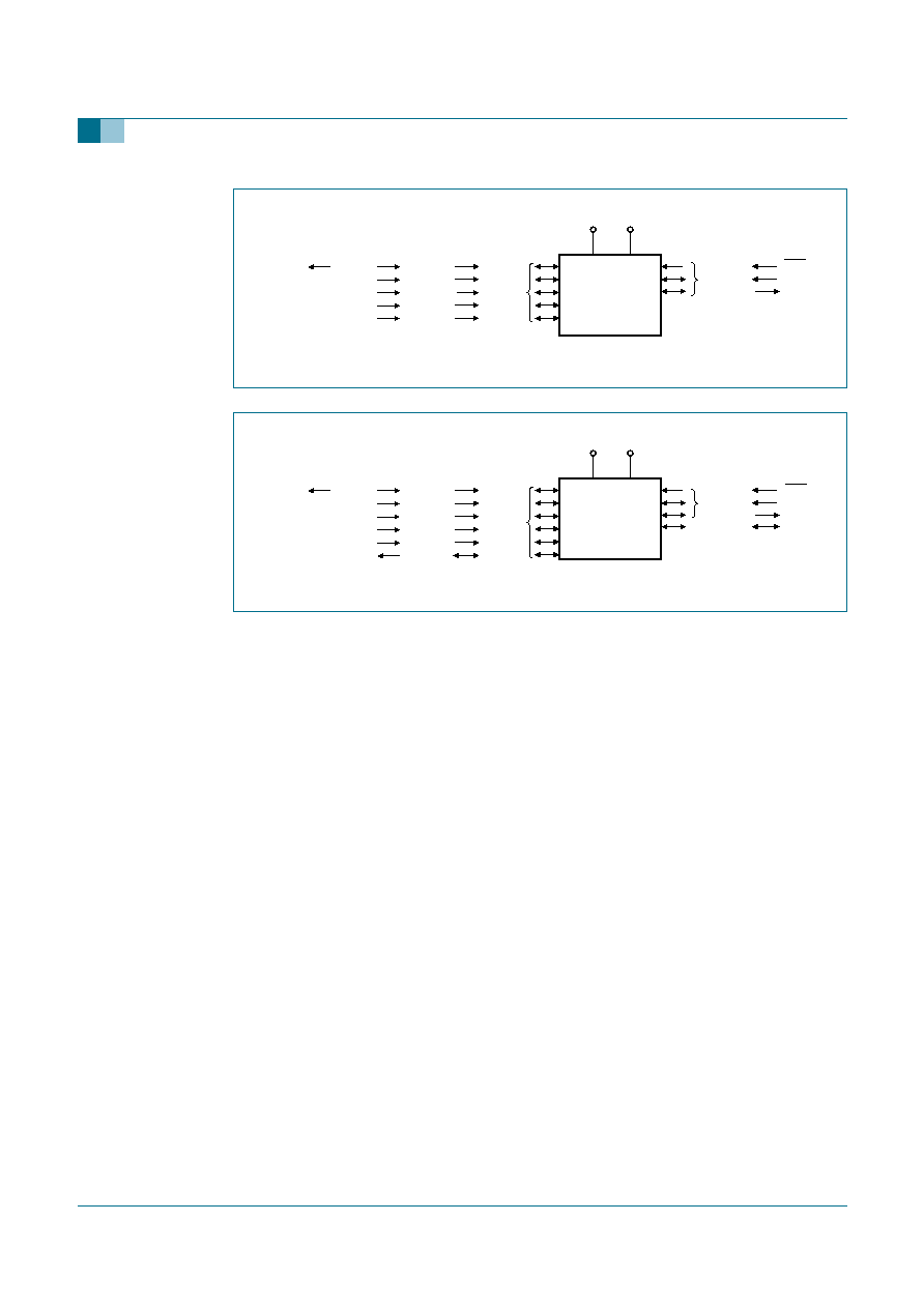
8.3 Clocks
8.3.1 Clock definitions
The P89LPC9102/9103/9107 device has internal clocks as defined below:
OSCCLK -- Input to the DIVM clock divider. OSCCLK is selected from one of the clock
sources (see
Figure 10 "Block diagram of P89LPC9102 oscillator control."
) and can also
be optionally divided to a slower frequency (see
Section 8.8 "CCLK modification: DIVM
register"
).
Note: f
osc
is defined as the OSCCLK frequency.
CCLK -- CPU clock; output of the clock divider. There are two CCLK cycles per machine
cycle, and most instructions are executed in one to two machine cycles (two or four CCLK
cycles).
RCCLK -- The internal 7.373 MHz RC oscillator output. The clock doubler option, when
enabled, provides an output frequency of 14.746 MHz.
PCLK -- Clock for the various peripheral devices and is
CCLK
/
2
.
8.3.2 CPU clock (OSCCLK)
The P89LPC9102/9103/9107 provides user-selectable oscillator options in generating the
CPU clock. This allows optimization for a range of needs from high precision to lowest
possible cost. These options are configured when the flash memory is programmed and
include an on-chip watchdog oscillator, an on-chip RC oscillator, and an external clock
input.
8.4 On-chip RC oscillator option
The P89LPC9102/9103/9107 has a 6-bit TRIM register that can be used to tune the
frequency of the RC oscillator. During reset, the TRIM value is initialized to a factory
pre-programmed value to adjust the oscillator frequency to 7.373 MHz
�
1 % at room
temperature. End-user applications can write to the Trim register to adjust the on-chip RC
oscillator to other frequencies. When the clock doubler option is enabled (UCFG1.3 = 1)
the output frequency is 14.746 MHz. If CCLK is 8 MHz or slower, the CLKLP SFR bit
(AUXR1.7) can be set to logic 1 to reduce power consumption. On reset, CLKLP is logic 0
allowing highest performance access. This bit can then be set in software if CCLK is
running at 8 MHz or slower.
The RCCLK bit (TRIM.7) can be used to switch between the clock source selected by
UCFG1 and the internal RC oscillator. This allows a low frequency source such as the
WDT or low speed external source to clock the device in order to save power and then
switch to the higher speed internal RC oscillator to perform processing.

9397 750 14655
� Koninklijke Philips Electronics N.V. 2005. All rights reserved.
Product data sheet
Rev. 02 -- 11 April 2005
27 of 58
Philips Semiconductors
P89LPC9102/9103/9107
8-bit microcontrollers with two-clock accelerated 80C51 core
8.5 Watchdog oscillator option
The watchdog timer has a separate oscillator which has a frequency of 400 kHz. This
oscillator can be used to save power when a high clock frequency is not needed.
8.6 External clock input option
In this configuration, the processor clock is derived from an external source driving the
P0.5/CMPREF/CLKIN pin. The rate may be from 0 Hz up to 18 MHz. The
P0.5/CMPREF/CLKIN pin may also be used as a standard port pin. When using an
oscillator frequency above 12 MHz, the reset input function of P1.5 must be
enabled. An external circuit is required to hold the device in reset at power-up until
V
DD
has reached its specified level. When system power is removed V
DD
will fall
below the minimum specified operating voltage. When using an oscillator
Fig 10. Block diagram of P89LPC9102 oscillator control.
Fig 11. Block diagram of P89LPC9103/9107 oscillator control.
�
2
002aaa973
RTC
CPU
WDT
DIVM
CCLK
OSCCLK
PCLK
TIMER 0
TIMER 1
WATCHDOG
OSCILLATOR
RC OSCILLATOR
WITH CLOCK
DOUBLER OPTION
(7.3728 MHz or
14.7456 MHz)
(400 kHz)
CLKIN
ADC1/
DAC1
�
2
002aaa974
RTC
CPU
WDT
DIVM
CCLK
OSCCLK
PCLK
TIMER 0
TIMER 1
WATCHDOG
OSCILLATOR
(400 kHz)
CLKIN
ADC1/
DAC1
BAUD RATE
GENERATOR
UART
RC OSCILLATOR
WITH CLOCK
DOUBLER OPTION
(7.3728 MHz or
14.7456 MHz)

9397 750 14655
� Koninklijke Philips Electronics N.V. 2005. All rights reserved.
Product data sheet
Rev. 02 -- 11 April 2005
28 of 58
Philips Semiconductors
P89LPC9102/9103/9107
8-bit microcontrollers with two-clock accelerated 80C51 core
frequency above 12 MHz, in some applications, an external brownout detect circuit
may be required to hold the device in reset when V
DD
falls below the minimum
specified operating voltage.
8.7 CCLK wake-up delay
The P89LPC9102/9103/9107 has an internal wake-up timer that delays the clock until it
stabilizes depending to the clock source used.
8.8 CCLK modification: DIVM register
The OSCCLK frequency can be divided down up to 510 times by configuring a dividing
register, DIVM, to generate CCLK. This feature makes it possible to temporarily run the
CPU at a lower rate, reducing power consumption. By dividing the clock, the CPU can
retain the ability to respond to events that would not exit Idle mode by executing its normal
program at a lower rate. This can also allow bypassing the oscillator start-up time in cases
where Power-down mode would otherwise be used. The value of DIVM may be changed
by the program at any time without interrupting code execution.
8.9 Low power select
If CCLK is 8 MHz or slower, the CLKLP SFR bit (AUXR1.7) can be set to logic 1 to lower
the power consumption further. On any reset, CLKLP is logic 0.
8.10 Memory organization
The various P89LPC9102/9103/9107 memory spaces are as follows:
�
DATA
128 bytes of internal data memory space (00h:7Fh) accessed via direct or indirect
addressing, using instruction other than MOVX and MOVC. All or part of the stack
may be in this area.
�
SFR
Special Function Registers. Selected CPU registers and peripheral control and status
registers, accessible only via direct addressing.
�
CODE
1 kB of Code memory space, accessed as part of program execution and via the
MOVC instruction.
8.11 Interrupts
The P89LPC9102 supports nine interrupt sources: timers 0 and 1, brownout detect,
watchdog timer/RTC, keyboard, comparator 1, and the A/D converter.
The P89LPC9103/9107 support nine interrupt sources: timers 0 and 1, serial port Tx,
serial port Rx, combined serial port Rx/Tx, brownout detect, watchdog timer/RTC,
keyboard, comparator, and the A/D converter.
Each interrupt source can be individually enabled or disabled by setting or clearing a bit in
the interrupt enable registers IEN0 or IEN1. The IEN0 register also contains a global
disable bit, EA, which disables all interrupts.
9397 750 14655
� Koninklijke Philips Electronics N.V. 2005. All rights reserved.
Product data sheet
Rev. 02 -- 11 April 2005
29 of 58
Philips Semiconductors
P89LPC9102/9103/9107
8-bit microcontrollers with two-clock accelerated 80C51 core
Each interrupt source can be individually programmed to one of four priority levels by
setting or clearing bits in the interrupt priority registers IP0, IP0H, IP1, and IP1H. An
interrupt service routine in progress can be interrupted by a higher priority interrupt, but
not by another interrupt of the same or lower priority. The highest priority interrupt service
cannot be interrupted by any other interrupt source. If two requests of different priority
levels are pending at the start of an instruction, the request of higher priority level is
serviced.
If requests of the same priority level are pending at the start of an instruction, an internal
polling sequence determines which request is serviced. This is called the arbitration
ranking. Note that the arbitration ranking is only used to resolve pending requests of the
same priority level.
8.11.1 External interrupt inputs
The P89LPC9102/9103/9107 has a Keypad Interrupt function. This can be used as an
external interrupt input.
If enabled when the P89LPC9102/9103/9107 is put into Power-down mode or Idle mode,
the interrupt will cause the processor to wake-up and resume operation. Refer to
Section
8.14 "Power reduction modes"
for details.
Fig 12. Interrupt sources, interrupt enables, and power-down wake-up sources (P89LPC9102).
002aaa976
BOF
EBO
KBIF
EKBI
interrupt
to CPU
wake-up
(if in power-down)
EWDRT
CMF
EC
EA (IE0.7)
RTCF
ERTC
(RTCCON.1)
WDOVF
TF1
ET1
TF0
ET0
ENADCI1
ADCI1
ENBI1
BNDI1
EAD
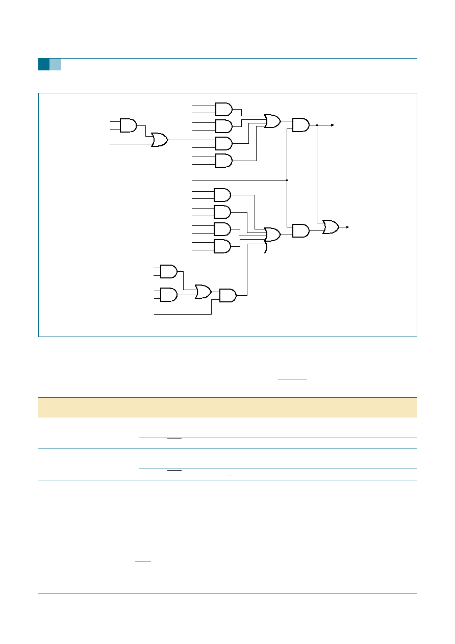
9397 750 14655
� Koninklijke Philips Electronics N.V. 2005. All rights reserved.
Product data sheet
Rev. 02 -- 11 April 2005
30 of 58
Philips Semiconductors
P89LPC9102/9103/9107
8-bit microcontrollers with two-clock accelerated 80C51 core
8.12 I/O ports
The P89LPC9102/9103/9107 has either 6, 7, or 8 I/O pins depending on the reset pin
option and clock source option chosen. Refer to
Table 10
.
[1]
Required for operation above 12 MHz.
8.12.1 Port configurations
All but one I/O port pin on the P89LPC9102/9103/9107 may be configured by software to
one of four types on a bit-by-bit basis. These are: quasi-bidirectional (standard 80C51 port
outputs), push-pull, open drain, and input-only. Two configuration registers for each port
select the output type for each port pin.
P1.5 (RST) can only be an input and cannot be configured.
Fig 13. Interrupt sources, interrupt enables, and power-down wake-up sources (P89LPC9103/9107).
002aaa977
BOF
EBO
KBIF
EKBI
interrupt
to CPU
wake-up
(if in power-down)
EWDRT
CMF
EC
EA (IE0.7)
RTCF
ERTC
(RTCCON.1)
WDOVF
TF1
ET1
TI and RI/RI
ES/ESR
TI
EST
TF0
ET0
ENADCI1
ADCI1
ENBI1
BNDI1
EAD
Table 10:
Number of I/O pins available
Clock source
Reset option
Number of I/O pins
(10-pin package)
Number of I/O pins
(14-pin package)
On-chip oscillator or watchdog
oscillator
No external reset (except during
power-up)
8
10
External RST pin supported
7
9
External clock input
No external reset (except during
power-up)
7
9
External RST pin supported
[1]
6
8

9397 750 14655
� Koninklijke Philips Electronics N.V. 2005. All rights reserved.
Product data sheet
Rev. 02 -- 11 April 2005
31 of 58
Philips Semiconductors
P89LPC9102/9103/9107
8-bit microcontrollers with two-clock accelerated 80C51 core
8.12.2 Quasi-bidirectional output configuration
Quasi-bidirectional output type can be used as both an input and output without the need
to reconfigure the port. This is possible because when the port outputs a logic HIGH, it is
weakly driven, allowing an external device to pull the pin LOW. When the pin is driven
LOW, it is driven strongly and able to sink a fairly large current. These features are
somewhat similar to an open-drain output except that there are three pull-up transistors in
the quasi-bidirectional output that serve different purposes.
The P89LPC9102/9103/9107 is a 3 V device, however, the pins are 5 V-tolerant. In
quasi-bidirectional mode, if a user applies 5 V on the pin, there will be a current flowing
from the pin to V
DD
, causing extra power consumption. Therefore, applying 5 V in
quasi-bidirectional mode is discouraged.
A quasi-bidirectional port pin has a Schmitt triggered input that also has a glitch
suppression circuit.
8.12.3 Open-drain output configuration
The open-drain output configuration turns off all pull-ups and only drives the pull-down
transistor of the port driver when the port latch contains a logic 0. To be used as a logic
output, a port configured in this manner must have an external pull-up, typically a resistor
tied to V
DD
.
An open-drain port pin has a Schmitt triggered input that also has a glitch suppression
circuit.
8.12.4 Input-only configuration
The input-only port configuration has no output drivers. It is a Schmitt triggered input that
also has a glitch suppression circuit.
8.12.5 Push-pull output configuration
The push-pull output configuration has the same pull-down structure as both the
open-drain and the quasi-bidirectional output modes, but provides a continuous strong
pull-up when the port latch contains a logic 1. The push-pull mode may be used when
more source current is needed from a port output. A push-pull port pin has a Schmitt
triggered input that also has a glitch suppression circuit.
8.12.6 Port 0 analog functions
The P89LPC9102/9103/9107 incorporates an Analog Comparator. In order to give the
best analog function performance and to minimize power consumption, pins that are being
used for analog functions must have the digital outputs and digital inputs disabled.
Digital outputs are disabled by putting the port output into the Input-only (high-impedance)
mode as described in
Section 8.12.4 "Input-only configuration"
.
Digital inputs on Port 0 may be disabled through the use of the PT0AD register. On any
reset, the PT0AD bits default to logic 0s to enable digital functions.
8.12.7 Additional port features
After power-up, all pins are in Input-only mode. Please note that this is different from
the LPC76x series of devices.

9397 750 14655
� Koninklijke Philips Electronics N.V. 2005. All rights reserved.
Product data sheet
Rev. 02 -- 11 April 2005
32 of 58
Philips Semiconductors
P89LPC9102/9103/9107
8-bit microcontrollers with two-clock accelerated 80C51 core
�
After power-up all I/O pins, except P1.5, may be configured by software.
�
Pin P1.5 is input-only.
Every output on the P89LPC9102/9103/9107 has been designed to sink typical LED drive
current. However, there is a maximum total output current for all ports which must not be
exceeded. Please refer to
Table 12 "Static characteristics"
for detailed specifications.
All ports pins that can function as an output have slew rate controlled outputs to limit noise
generated by quickly switching output signals. The slew rate is factory-set to
approximately 10 ns rise and fall times.
8.13 Power monitoring functions
The P89LPC9102/9103/9107 incorporates power monitoring functions designed to
prevent incorrect operation during initial power-up and power loss or reduction during
operation. This is accomplished with two hardware functions: Power-on Detect and
Brownout detect.
8.13.1 Brownout detection
The Brownout detect function determines if the power supply voltage drops below a
certain level. The default operation is for a Brownout detection to cause a processor reset,
however, it may alternatively be configured to generate an interrupt.
Brownout detection may be enabled or disabled in software.
If Brownout detection is enabled, the brownout condition occurs when V
DD
falls below the
brownout trip voltage, V
BO
(see
Table 12 "Static characteristics"
), and is negated when
V
DD
rises above V
BO
. If the P89LPC9102/9103/9107 device is to operate with a power
supply that can be below 2.7 V, Brownout detect Enable (BOE) should be left in the
unprogrammed state so that the device can operate at 2.4 V, otherwise continuous
brownout reset may prevent the device from operating.
For correct activation of Brownout detect, the V
DD
rise and fall times must be observed.
Please see
Table 12 "Static characteristics"
for specifications.
8.13.2 Power-on detection
The Power-on Detect has a function similar to the Brownout detect, but is designed to
work as power comes up initially, before the power supply voltage reaches a level where
Brownout detect can work. The Power-on detect flag (POF) in the RSTSRC register is set
to indicate an initial power-up condition. The POF flag will remain set until cleared by
software.
8.14 Power reduction modes
The P89LPC9102/9103/9107 supports three different power reduction modes. These
modes are Idle mode, Power-down mode, and Total Power-down mode.
8.14.1 Idle mode
Idle mode leaves peripherals running in order to allow them to activate the processor
when an interrupt is generated. Any enabled interrupt source or reset may terminate Idle
mode.

9397 750 14655
� Koninklijke Philips Electronics N.V. 2005. All rights reserved.
Product data sheet
Rev. 02 -- 11 April 2005
33 of 58
Philips Semiconductors
P89LPC9102/9103/9107
8-bit microcontrollers with two-clock accelerated 80C51 core
8.14.2 Slow-down mode using the DIVM register
Slow-down mode is achieved by dividing down the OSCCLK frequency to generate CCLK.
This division is accomplished by configuring the DIVM register to divide OSCCLK by up to
510 times. This feature makes it possible to temporarily run the CPU at a lower rate,
reducing power consumption. By dividing the clock, the CPU can retain the ability to
respond to events that would not exit Idle mode by executing its normal program at a lower
rate. This can also allow bypassing the oscillator start-up time in cases where
Power-down mode would otherwise be used. The value of DIVM may be changed by the
program at any time without interrupting code execution.
8.14.3 Power-down mode
The Power-down mode stops the oscillator in order to minimize power consumption. The
P89LPC9102/9103/9107 exits Power-down mode via any reset, or certain interrupts. In
Power-down mode, the power supply voltage may be reduced to the data retention
voltage V
DDR
. This retains the RAM contents at the point where Power-down mode was
entered. SFR contents are not guaranteed after V
DD
has been lowered to V
DDR
, therefore
it is highly recommended to wake-up the processor via reset in this case. V
DD
must be
raised to within the operating range before the Power-down mode is exited.
Some chip functions continue to operate and draw power during Power-down mode,
increasing the total power used during Power-down mode. These include: Brownout
detect, watchdog timer, Comparators (note that Comparator can be powered-down
separately), and RTC/system timer. The internal RC oscillator is disabled unless both the
RC oscillator has been selected as the system clock and the RTC is enabled.
8.14.4 Total Power-down mode
This is the same as Power-down mode except that the brownout detection circuitry and
the voltage comparators are also disabled to conserve additional power. The internal RC
oscillator is disabled unless both the RC oscillator has been selected as the system clock
and the RTC is enabled. If the internal RC oscillator is used to clock the RTC during
Power-down mode, there will be high power consumption. Please use an external low
frequency clock to achieve low power with the RTC running during Power-down mode.
8.15 Reset
The P1.5/RST pin can function as either an active-LOW reset input or as a digital input,
P1.5. The RPE (Reset Pin Enable) bit in UCFG1, when set to logic 1, enables the external
reset input function on P1.5. When cleared, P1.5 may be used as an input pin.
Remark: During a power-up sequence, the RPE selection is overridden and this pin will
always function as a reset input. An external circuit connected to this pin should not
hold this pin LOW during a power-on sequence as this will keep the device in reset.
After power-up this input will function either as an external reset input or as a digital input
as defined by the RPE bit. Only a power-up reset will temporarily override the selection
defined by RPE bit. Other sources of reset will not override the RPE bit.
Remark: During a power cycle, V
DD
must fall below V
POR
(see
Table 12 "Static
characteristics"
) before power is reapplied, in order to ensure a power-on reset.
Reset can be triggered from the following sources:
�
External reset pin (during power-up or if user configured via UCFG1)

9397 750 14655
� Koninklijke Philips Electronics N.V. 2005. All rights reserved.
Product data sheet
Rev. 02 -- 11 April 2005
34 of 58
Philips Semiconductors
P89LPC9102/9103/9107
8-bit microcontrollers with two-clock accelerated 80C51 core
�
Power-on detect
�
Brownout detect
�
Watchdog timer
�
Software reset
�
UART break character detect reset (P89LPC9103/9107).
For every reset source, there is a flag in the Reset Register, RSTSRC. The user can read
this register to determine the most recent reset source. These flag bits can be cleared in
software by writing a logic 0 to the corresponding bit. More than one flag bit may be set:
�
During a power-on reset, both POF and BOF are set but the other flag bits are
cleared.
�
For any other reset, previously set flag bits that have not been cleared will remain set.
8.16 Timers 0 and 1
The P89LPC9102 has two general purpose timer/counters which are similar to the
standard 80C51 Timer 0 and Timer 1. These timers have five operating modes (modes 0,
1, 2, 3, and 6). Modes 0, 1, and 2 are the same for both Timers. Mode 3 is different.
The P89LPC9103/9107 has two general purpose timers which are similar to the standard
80C51 Timer 0 and Timer 1. These timers have four operating modes (modes 0, 1, 2, and
3). Modes 0, 1, and 2 are the same for both Timers. Mode 3 is different.
8.16.1 Mode 0
Putting either Timer into Mode 0 makes it look like an 8048 Timer, which is an 8-bit
Counter with a divide-by-32 prescaler. In this mode, the Timer register is configured as a
13-bit register. Mode 0 operation is the same for Timer 0 and Timer 1.
8.16.2 Mode 1
Mode 1 is the same as Mode 0, except that all 16 bits of the timer register are used.
8.16.3 Mode 2
Mode 2 configures the Timer register as an 8-bit counter with automatic reload. Mode 2
operation is the same for Timer 0 and Timer 1.
8.16.4 Mode 3
When Timer 1 is in Mode 3 it is stopped. Timer 0 in Mode 3 forms two separate 8-bit
counters and is provided for applications that require an extra 8-bit timer. When Timer 1 is
in Mode 3 it can still be used by the serial port as a baud rate generator.
8.16.5 Mode 6 (P89LPC9102/9107)
In this mode, the corresponding timer can be changed to a PWM with a full period of
256 timer clocks.

9397 750 14655
� Koninklijke Philips Electronics N.V. 2005. All rights reserved.
Product data sheet
Rev. 02 -- 11 April 2005
35 of 58
Philips Semiconductors
P89LPC9102/9103/9107
8-bit microcontrollers with two-clock accelerated 80C51 core
8.16.6 Timer overflow toggle output (P89LPC9102/9107)
Timers 0 and 1 can be configured to automatically toggle a port output whenever a timer
overflow occurs. The same device pins that are used for the T0 and T1 count inputs are
also used for the timer toggle outputs. The port outputs will be a logic 1 prior to the first
timer overflow when this mode is turned on.
8.17 RTC/system timer
The P89LPC9102/9103/9107 has a simple RTC that allows a user to continue running an
accurate timer while the rest of the device is powered-down. The RTC can be a wake-up
or an interrupt source. The RTC is a 23-bit down counter comprised of a 7-bit prescaler
and a 16-bit loadable down counter. When it reaches all logic 0s, the counter will be
reloaded again and the RTCF flag will be set. The clock source for this counter is the
CCLK. Only power-on reset will reset the RTC and its associated SFRs to the default
state.
8.18 UART (P89LPC9103/9107)
The P89LPC9103/9107 has an enhanced UART that is compatible with the conventional
80C51 UART except that Timer 2 overflow cannot be used as a baud rate source. The
P89LPC9103/9107 does include an independent Baud Rate Generator. The baud rate
can be selected from CCLK (divided by a constant), Timer 1 overflow, or the independent
Baud Rate Generator. In addition to the baud rate generation, enhancements over the
standard 80C51 UART include Framing Error detection, automatic address recognition,
selectable double buffering and several interrupt options. The UART can be operated in
four modes: shift register, 8-bit UART, 9-bit UART, and
CCLK
/
32
or
CCLK
/
16
.
8.18.1 Mode 0
Serial data enters and exits through RXD. TXD outputs the shift clock. Eight bits are
transmitted or received, LSB first. The baud rate is fixed at
1
/
16
of the CPU clock
frequency.
8.18.2 Mode 1
10 bits are transmitted (through TXD) or received (through RXD): a start bit (logic 0),
8 data bits (LSB first), and a stop bit (logic 1). When data is received, the stop bit is stored
in RB8 in Special Function Register SCON. The baud rate is variable and is determined
by the Timer 1 overflow rate or the Baud Rate Generator (described in
Section 8.18.5
"Baud rate generator and selection"
).
8.18.3 Mode 2
11 bits are transmitted (through TXD) or received (through RXD): start bit (logic 0), 8 data
bits (LSB first), a programmable 9
th
data bit, and a stop bit (logic 1). When data is
transmitted, the 9
th
data bit (TB8 in SCON) can be assigned the value of logic 0 or logic 1.
Or, for example, the parity bit (P, in the PSW) could be moved into TB8. When data is
received, the 9
th
data bit goes into RB8 in Special Function Register SCON, while the stop
bit is not saved. The baud rate is programmable to either
1
/
16
or
1
/
32
of the CPU clock
frequency, as determined by the SMOD1 bit in PCON.
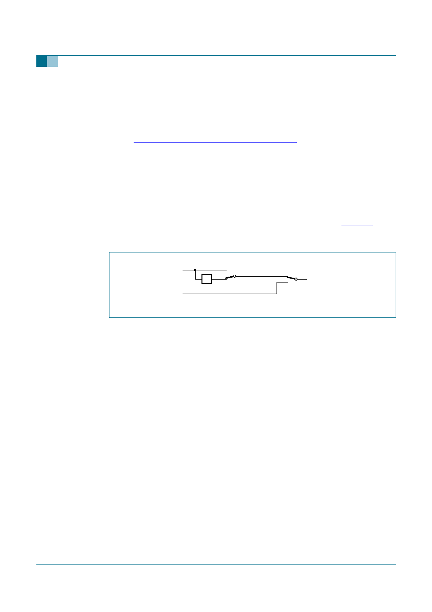
9397 750 14655
� Koninklijke Philips Electronics N.V. 2005. All rights reserved.
Product data sheet
Rev. 02 -- 11 April 2005
36 of 58
Philips Semiconductors
P89LPC9102/9103/9107
8-bit microcontrollers with two-clock accelerated 80C51 core
8.18.4 Mode 3
11 bits are transmitted (through TXD) or received (through RXD): a start bit (logic 0), 8
data bits (LSB first), a programmable 9
th
data bit, and a stop bit (logic 1). In fact, Mode 3 is
the same as Mode 2 in all respects except baud rate. The baud rate in Mode 3 is variable
and is determined by the Timer 1 overflow rate or the Baud Rate Generator (described in
section
Section 8.18.5 "Baud rate generator and selection"
).
8.18.5 Baud rate generator and selection
The P89LPC9103/9107 enhanced UART has an independent Baud Rate Generator. The
baud rate is determined by a baud-rate preprogrammed into the BRGR1 and BRGR0
SFRs which together form a 16-bit baud rate divisor value that works in a similar manner
as Timer 1. If the baud rate generator is used, Timer 1 can be used for other timing
functions.
The UART can use either Timer 1 or the baud rate generator output (see
Figure 14
). Note
that Timer T1 is further divided by 2 if the SMOD1 bit (PCON.7) is cleared. The
independent Baud Rate Generator uses CCLK.
8.18.6 Framing error
Framing error is reported in the status register (SSTAT). In addition, if SMOD0 (PCON.6)
is logic 1, framing errors can be made available in SCON.7, respectively. If SMOD0 is
logic 0, SCON.7 is SM0. It is recommended that SM0 and SM1 (SCON[7:6]) are set up
when SMOD0 is logic 0.
8.18.7 Break detect
Break detect is reported in the status register (SSTAT). A break is detected when
11 consecutive bits are sensed LOW. The break detect can be used to reset the device.
8.18.8 Double buffering
The UART has a transmit double buffer that allows buffering of the next character to be
written to SBUF while the first character is being transmitted. Double buffering allows
transmission of a string of characters with only one stop bit between any two characters,
as long as the next character is written between the start bit and the stop bit of the
previous character.
Double buffering can be disabled. If disabled (DBMOD, i.e., SSTAT.7 = 0), the UART is
compatible with the conventional 80C51 UART. If enabled, the UART allows writing to
SnBUF while the previous data is being shifted out. Double buffering is only allowed in
Modes 1, 2 and 3. When operated in Mode 0, double buffering must be disabled
(DBMOD = 0).
Fig 14. Baud rate sources for UART (Modes 1, 3).
baud rate modes 1 and 3
SBRGS = 1
SBRGS = 0
SMOD1 = 0
SMOD1 = 1
timer 1 overflow
(PCLK-based)
baud rate generator
(CCLK-based)
002aaa978
�
2
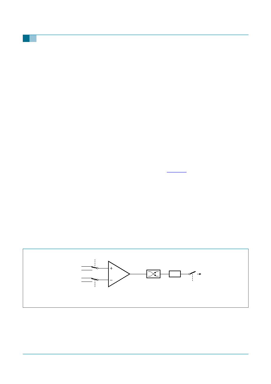
9397 750 14655
� Koninklijke Philips Electronics N.V. 2005. All rights reserved.
Product data sheet
Rev. 02 -- 11 April 2005
37 of 58
Philips Semiconductors
P89LPC9102/9103/9107
8-bit microcontrollers with two-clock accelerated 80C51 core
8.18.9 Transmit interrupts with double buffering enabled (Modes 1, 2 and 3)
Unlike the conventional UART, in double buffering mode, the Tx interrupt is generated
when the double buffer is ready to receive new data.
8.18.10 The 9
th
bit (bit 8) in double buffering (Modes 1, 2 and 3)
If double buffering is disabled TB8 can be written before or after SBUF is written, as long
as TB8 is updated some time before that bit is shifted out. TB8 must not be changed until
the bit is shifted out, as indicated by the Tx interrupt.
If double buffering is enabled, TB8 must be updated before SBUF is written, as TB8 will
be double-buffered together with SBUF data.
8.19 Analog comparators
One analog comparator is provided on the P89LPC9102/9103/9107. Comparator
operation is such that the output is a logic 1 (which may be read in a register) when the
positive input is greater than the negative input (selectable from a pin or an internal
reference voltage). Otherwise the output is a zero. The comparator may be configured to
cause an interrupt when the output value changes.
The connections to the comparator are shown in
Figure 15
. The comparator functions to
V
DD
= 2.4 V.
When the comparator is first enabled, the comparator's interrupt flag is not guaranteed to
be stable for 10 microseconds. The comparator interrupt should not be enabled during
that time, and the comparator interrupt flag must be cleared before the interrupt is enabled
in order to prevent an immediate interrupt service.
When a comparator is disabled the comparator's output, COx, goes HIGH. If the
comparator output was LOW and then is disabled, the resulting transition of the
comparator output from a LOW to HIGH state will set the comparator flag, CMFx. This will
cause an interrupt if the comparator interrupt is enabled. The user should therefore
disable the comparator interrupt prior to disabling the comparator. Additionally, the user
should clear the comparator flag, CMFx, after disabling the comparator.
8.20 Internal reference voltage
An internal reference voltage generator may supply a default reference when a single
comparator input pin is used. The value of the internal reference voltage, referred to as
V
REF
, is 1.23 V
�
10 %.
Fig 15. Comparator input and output connections.
comparator
CN1
(P0.4) CIN1A
(P0.3) CIN1B
(P0.5) CMPREF
V
REF
CO1
002aaa979
change detect
CMF1
interrupt
EC
CP1

9397 750 14655
� Koninklijke Philips Electronics N.V. 2005. All rights reserved.
Product data sheet
Rev. 02 -- 11 April 2005
38 of 58
Philips Semiconductors
P89LPC9102/9103/9107
8-bit microcontrollers with two-clock accelerated 80C51 core
8.21 Comparator interrupt
The comparator has an interrupt flag contained in its configuration register. This flag is set
whenever the comparator output changes state. The flag may be polled by software or
may be used to generate an interrupt.
8.22 Comparator and power reduction modes
The comparator may remain enabled when Power-down mode or Idle mode is activated,
but the comparator is disabled automatically in Total Power-down mode.
If the comparator interrupt is enabled (except in Total Power-down mode), a change of the
comparator output state will generate an interrupt and wake-up the processor. If the
comparator output to a pin is enabled, the pin should be configured in the push-pull mode
in order to obtain fast switching times while in Power-down mode. The reason is that with
the oscillator stopped, the temporary strong pull-up that normally occurs during switching
on a quasi-bidirectional port pin does not take place.
The comparator consumes power in Power-down mode and Idle mode, as well as in the
normal operating mode. This fact should be taken into account when system power
consumption is an issue. To minimize power consumption, the user can disable the
comparator via PCONA.5 or put the device in Total Power-down mode.
8.23 Keypad interrupt (KBI)
The Keypad Interrupt function is intended primarily to allow a single interrupt to be
generated when Port 0 is equal to or not equal to a certain pattern. This function can be
used for bus address recognition or keypad recognition. The user can configure the port
via SFRs for different tasks.
The Keypad Interrupt Mask Register (KBMASK) is used to define which input pins
connected to Port 0 can trigger the interrupt. The Keypad Pattern Register (KBPATN) is
used to define a pattern that is compared to the value of Port 0. The Keypad Interrupt Flag
(KBIF) in the Keypad Interrupt Control Register (KBCON) is set when the condition is
matched while the Keypad Interrupt function is active. An interrupt will be generated if
enabled. The PATN_SEL bit in the Keypad Interrupt Control Register (KBCON) is used to
define equal or not-equal for the comparison.
In order to use the Keypad Interrupt as an original KBI function like in 87LPC76x series,
the user needs to set KBPATN = 0FFH and PATN_SEL = 1 (not equal), then any key
connected to Port 0 which is enabled by the KBMASK register will cause the hardware to
set KBIF and generate an interrupt if it has been enabled. The interrupt may be used to
wake-up the CPU from Idle mode or Power-down mode. This feature is particularly useful
in handheld, battery powered systems that need to carefully manage power consumption
yet also need to be convenient to use.
In order to set the flag and cause an interrupt, the pattern on Port 0 must be held longer
than six CCLKs.
8.24 Watchdog timer
The watchdog timer causes a system reset when it underflows as a result of a failure to
feed the timer prior to the timer reaching its terminal count. It consists of a programmable
12-bit prescaler, and an 8-bit down counter. The down counter is decremented by a tap
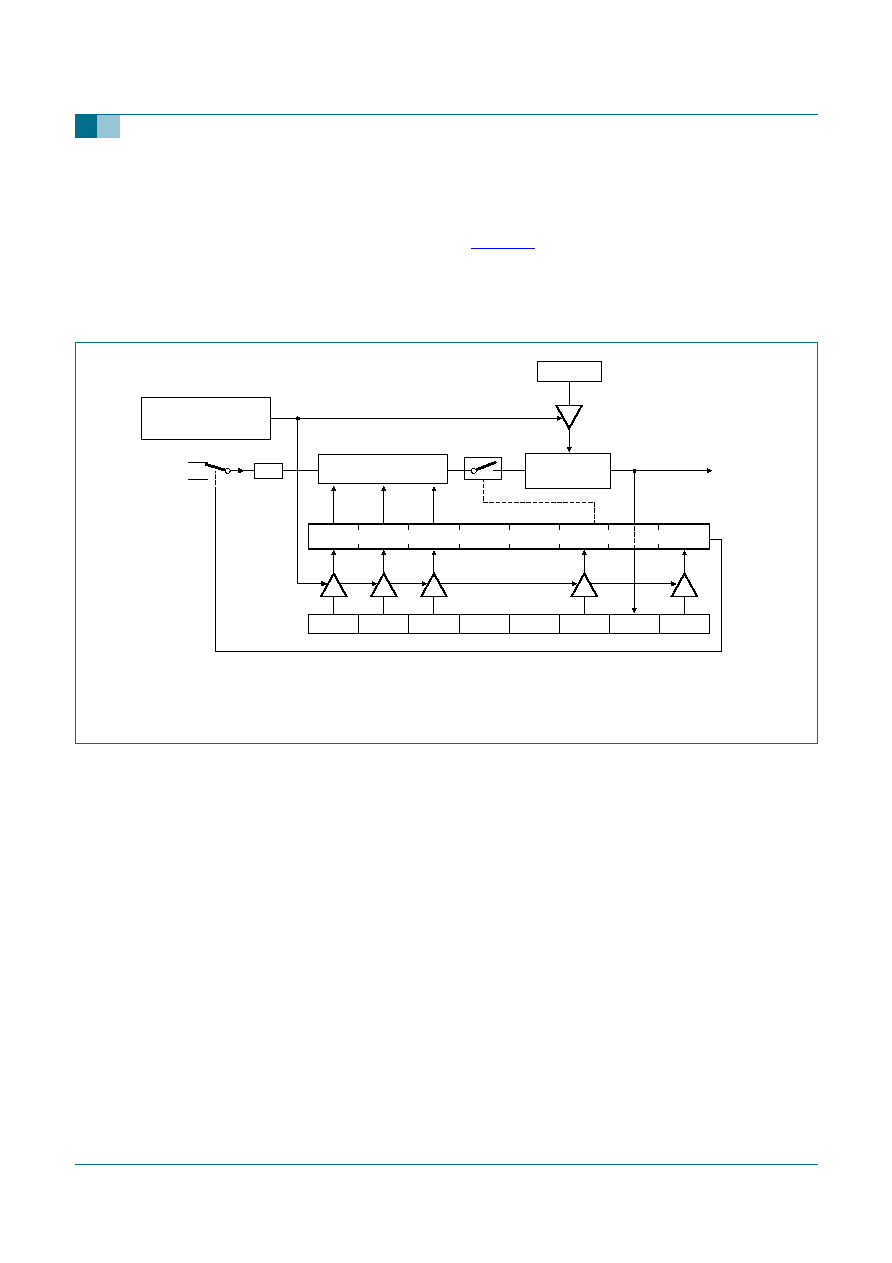
9397 750 14655
� Koninklijke Philips Electronics N.V. 2005. All rights reserved.
Product data sheet
Rev. 02 -- 11 April 2005
39 of 58
Philips Semiconductors
P89LPC9102/9103/9107
8-bit microcontrollers with two-clock accelerated 80C51 core
taken from the prescaler. The clock source for the prescaler is either the PCLK or the
nominal 400 kHz watchdog oscillator. The watchdog timer can only be reset by a
power-on reset. When the watchdog timer feature is disabled, it can be used as an interval
timer and may generate an interrupt.
Figure 16
shows the watchdog timer in Watchdog
mode. Feeding the watchdog timer requires a two-byte sequence. If PCLK is selected as
the watchdog timer clock and the CPU is powered-down, the watchdog timer is disabled.
The watchdog timer has a time-out period that ranges from a few
�
s to a few seconds.
Please refer to the
P89LPC9102/9103/9107 User manual for more details.
8.25 Additional features
8.25.1 Software reset
The SRST bit in AUXR1 gives software the opportunity to reset the processor completely,
as if an external reset or watchdog timer reset had occurred. Care should be taken when
writing to AUXR1 to avoid accidental software resets.
8.25.2 Dual data pointers
The dual Data Pointers (DPTR) provides two different Data Pointers to specify the address
used with certain instructions. The DPS bit in the AUXR1 register selects one of the two
Data Pointers. Bit 2 of AUXR1 is permanently wired as a logic 0 so that the DPS bit may
be toggled (thereby switching Data Pointers) simply by incrementing the AUXR1 register,
without the possibility of inadvertently altering other bits in the register.
(1) Watchdog timer reset can also be caused by an invalid feed sequence, or by writing to WDCON not immediately followed by
a feed sequence.
Fig 16. Watchdog timer in Watchdog mode (WDTE = 1).
PRE2
PRE1
PRE0
-
-
WDRUN
WDTOF
WDCLK
WDCON (A7H)
SHADOW REGISTER
PRESCALER
002aaa980
8-BIT DOWN
COUNTER
WDL (C1H)
watchdog
oscillator
PCLK
�
32
MOV WFEED1, #0A5H
MOV WFEED2, #05AH
reset (1)

9397 750 14655
� Koninklijke Philips Electronics N.V. 2005. All rights reserved.
Product data sheet
Rev. 02 -- 11 April 2005
40 of 58
Philips Semiconductors
P89LPC9102/9103/9107
8-bit microcontrollers with two-clock accelerated 80C51 core
8.26 Flash program memory
8.26.1 General description
The P89LPC9102/9103/9107 Flash memory provides in-circuit electrical erasure and
programming. The Flash can be erased, read, and written as bytes. The Sector and Page
Erase functions can erase any Flash sector (256 bytes) or page (16 bytes). The Chip
Erase operation will erase the entire program memory. In-Circuit Programming using
standard commercial programmers is available. In addition, In-Application Programming
Lite (IAP-Lite) and byte erase allows code memory to be used for non-volatile data
storage. On-chip erase and write timing generation contribute to a user-friendly
programming interface. The P89LPC9102/9103/9107 Flash reliably stores memory
contents even after more than 100,000 erase and program cycles. The cell is designed to
optimize the erase and programming mechanisms. The P89LPC9102/9103/9107 uses
V
DD
as the supply voltage to perform the Program/Erase algorithms.
8.26.2 Features
�
Programming and erase over the full operating voltage range.
�
Byte-erase allowing code memory to be used for data storage.
�
Read/Programming/Erase using ICP.
�
Any Flash program/erase operation in 2 ms.
�
Programming with industry-standard commercial programmers.
�
Programmable security for the code in the Flash for each sector.
�
More than 100,000 minimum erase/program cycles for each byte.
�
10-year minimum data retention.
8.26.3 Flash organization
The P89LPC9102/9103/9107 program memory consists of four 256 byte sectors. Each
sector can be further divided into 16-byte pages. In addition to sector erase, page erase,
and byte erase, a 16-byte page register is included which allows from 1 byte to 16 bytes of
a given page to be programmed at the same time, substantially reducing overall
programming time. In addition, erasing and reprogramming of user-programmable
configuration bytes including UCFG1, the Boot Status Bit, and the Boot Vector is
supported.
8.26.4 Flash programming and erasing
Different methods of erasing or programming of the Flash are available. The Flash may be
programmed or erased in the end-user application (IAP-Lite) under control of the
application's firmware. Another option is to use the ICP mechanism. This ICP system
provides for programming through a serial clock- serial data interface. Third, the Flash
may be programmed or erased using a commercially available EPROM programmer
which supports this device. This device does not provide for direct verification of code
memory contents. Instead this device provides a 32-bit CRC result on either a sector or
the entire 1 kB of user code space.

9397 750 14655
� Koninklijke Philips Electronics N.V. 2005. All rights reserved.
Product data sheet
Rev. 02 -- 11 April 2005
41 of 58
Philips Semiconductors
P89LPC9102/9103/9107
8-bit microcontrollers with two-clock accelerated 80C51 core
8.26.5 In-circuit programming
In-Circuit Programming is performed without removing the microcontroller from the
system. The In-Circuit Programming facility consists of internal hardware resources to
facilitate remote programming of the P89LPC9102/9103/9107 through a two-wire serial
interface. The Philips In-Circuit Programming facility has made in-circuit programming in
an embedded application, using commercially available programmers, possible with a
minimum of additional expense in components and circuit board area. The ICP function
uses five pins. Only a small connector needs to be available to interface your application
to a commercial programmer in order to use this feature. Additional details may be found
in the
P89LPC9102/9103/9107 User manual.
8.26.6 In-application programming (IAP-Lite)
In-Application Programming is performed in the application under the control of the
microcontroller's firmware. The IAP facility consists of internal hardware resources to
facilitate programming and erasing. The Philips In-Application Programming (IAP-Lite)
has made in-application programming in an embedded application possible without
additional components. This is accomplished through the use of four SFRs consisting of a
control/status register, a data register, and two address registers. Additional details may
be found in the
P89LPC9102/9103/9107 User manual.
8.26.7 Using Flash as data storage
The Flash code memory array of this device supports individual byte erasing and
programming. Any byte in the code memory array may be read using the MOVC
instruction, provided that the sector containing the byte has not been secured (a MOVC
instruction is not allowed to read code memory contents of a secured sector). Thus any
byte in a non-secured sector may be used for non-volatile data storage.
8.26.8 User configuration bytes
Some user-configurable features of the P89LPC9102/9103/9107 must be defined at
power-up and therefore cannot be set by the program after start of execution. These
features are configured through the use of the Flash byte UCFG1. Please see the
P89LPC9102/9103/9107 User manual for additional details.
8.26.9 User sector security bytes
There are four user sector security bytes, each corresponding to one sector. Please see
the
P89LPC9102/9103/9107 User manual for additional details.

9397 750 14655
� Koninklijke Philips Electronics N.V. 2005. All rights reserved.
Product data sheet
Rev. 02 -- 11 April 2005
42 of 58
Philips Semiconductors
P89LPC9102/9103/9107
8-bit microcontrollers with two-clock accelerated 80C51 core
9.
A/D Converter
9.1 General description
The P89LPC9102/9103/9107 has an 8-bit, 4-channel multiplexed successive
approximation analog-to-digital converter. The A/D consists of a 4-input multiplexer which
feeds a sample-and-hold circuit providing an input signal to one of two comparator inputs.
The control logic in combination with the Successive Approximation Register (SAR) drives
a digital-to-analog converter which provides the other input to the comparator. The output
of the comparator is fed to the SAR. A block diagram of the A/D converter is shown in
Figure 17
.
9.2 Features
s
8-bit, 4-channel multiplexed input, successive approximation A/D converter
s
Four result registers
s
Six operating modes
x
Fixed channel, single conversion mode
x
Fixed channel, continuous conversion mode
x
Auto scan, single conversion mode
x
Auto scan, continuous conversion mode
x
Dual channel, continuous conversion mode
x
Single step mode
s
Three conversion start modes
x
Timer triggered start
x
Start immediately
s
8-bit conversion time of
3.9
�
s at an ADC clock of 3.3 MHz
s
Interrupt or polled operation
s
Boundary limits interrupt
s
DAC output to a port pin with high output impedance
s
Clock divider
s
Power-down mode

9397 750 14655
� Koninklijke Philips Electronics N.V. 2005. All rights reserved.
Product data sheet
Rev. 02 -- 11 April 2005
43 of 58
Philips Semiconductors
P89LPC9102/9103/9107
8-bit microcontrollers with two-clock accelerated 80C51 core
9.3 Block diagram
9.4 A/D operating modes
9.4.1 Fixed channel, single conversion mode
A single input channel can be selected for conversion. A single conversion will be
performed and the result placed in the result register which corresponds to the selected
input channel. An interrupt, if enabled, will be generated after the conversion completes.
9.4.2 Fixed channel, continuous conversion mode
A single input channel can be selected for continuous conversion. The results of the
conversions will be sequentially placed in the four result registers. An interrupt, if enabled,
will be generated after every four conversions. Additional conversion results will again
cycle through the four result registers, overwriting the previous results. Continuous
conversions continue until terminated by the user.
9.4.3 Auto scan, single conversion mode
Any combination of the four input channels can be selected for conversion. A single
conversion of each selected input will be performed and the result placed in the result
register which corresponds to the selected input channel. An interrupt, if enabled, will be
generated after all selected channels have been converted. If only a single channel is
selected this is equivalent to single channel, single conversion mode.
9.4.4 Auto scan, continuous conversion mode
Any combination of the four input channels can be selected for conversion. A conversion
of each selected input will be performed and the result placed in the result register which
corresponds to the selected input channel. An interrupt, if enabled, will be generated after
all selected channels have been converted. The process will repeat starting with the first
selected channel. Additional conversion results will again cycle through the four result
registers, overwriting the previous results. Continuous conversions continue until
terminated by the user.
Fig 17. ADC block diagram.
+
�
comp
DAC1
SAR
8
INPUT
MUX
CONTROL
LOGIC
CCLK
002aaa975

9397 750 14655
� Koninklijke Philips Electronics N.V. 2005. All rights reserved.
Product data sheet
Rev. 02 -- 11 April 2005
44 of 58
Philips Semiconductors
P89LPC9102/9103/9107
8-bit microcontrollers with two-clock accelerated 80C51 core
9.4.5 Dual channel, continuous conversion mode
This is a variation of the auto scan continuous conversion mode where conversion occurs
on two user-selectable inputs. The result of the conversion of the first channel is placed in
result register, AD1DAT0. The result of the conversion of the second channel is placed in
result register, AD1DAT1. The first channel is again converted and its result stored in
AD1DAT2. The second channel is again converted and its result placed in AD1DAT3. An
interrupt is generated, if enabled, after every set of four conversions (two conversions per
channel).
9.4.6 Single step mode
This special mode allows `single-stepping' in an auto scan conversion mode. Any
combination of the four input channels can be selected for conversion. After each channel
is converted, an interrupt is generated, if enabled, and the A/D waits for the next start
condition. May be used with any of the start modes.
9.5 Conversion start modes
9.5.1 Timer triggered start
An A/D conversion is started by the overflow of Timer 0. Once a conversion has started,
additional Timer 0 triggers are ignored until the conversion has completed. The Timer
triggered start mode is available in all A/D operating modes.
9.5.2 Start immediately
Programming this mode immediately starts a conversion. This start mode is available in all
A/D operating modes.
9.6 Boundary limits interrupt
The A/D converter has both a high and low boundary limit register. After the four MSBs
have been converted, these four bits are compared with the four MSBs of the boundary
high and low registers. If the four MSBs of the conversion are outside the limit an interrupt
will be generated, if enabled. If the conversion result is within the limits, the boundary
limits will again be compared after all 8 bits have been converted. An interrupt will be
generated, if enabled, if the result is outside the boundary limits. The boundary limit may
be disabled by clearing the boundary limit interrupt enable.
9.7 DAC output to a port pin with high output impedance
The A/D converter's DAC block can be output to a port pin. In this mode, the AD1DAT3
register is used to hold the value fed to the DAC. After a value has been written to the DAC
(written to AD1DAT3), the DAC output will appear on the channel 3 pin.
9.8 Clock divider
The A/D converter requires that its internal clock source be in the range of 500 kHz to
3.3 MHz to maintain accuracy. A programmable clock divider that divides the clock
from 1 to 8 is provided for this purpose.

9397 750 14655
� Koninklijke Philips Electronics N.V. 2005. All rights reserved.
Product data sheet
Rev. 02 -- 11 April 2005
45 of 58
Philips Semiconductors
P89LPC9102/9103/9107
8-bit microcontrollers with two-clock accelerated 80C51 core
9.9 Power-down and Idle mode
In Idle mode the A/D converter, if enabled, will continue to function and can cause the
device to exit Idle mode when the conversion is completed if the A/D interrupt is enabled.
In Power-down mode or Total Power-down mode, the A/D does not function. If the A/D is
enabled, it will consume power. Power can be reduced by disabling the A/D.

9397 750 14655
� Koninklijke Philips Electronics N.V. 2005. All rights reserved.
Product data sheet
Rev. 02 -- 11 April 2005
46 of 58
Philips Semiconductors
P89LPC9102/9103/9107
8-bit microcontrollers with two-clock accelerated 80C51 core
10. Limiting values
[1]
The following applies to
Table 11 "Limiting values"
:
a) Stresses above those listed may cause permanent damage to the device. This is a stress rating only and functional operation of the
device at these or any conditions other than those described in
Table 12 "Static characteristics"
and
Table 13 "Dynamic
characteristics (12 MHz)"
section of this specification are not implied.
b) This product includes circuitry specifically designed for the protection of its internal devices from the damaging effects of excessive
static charge. Nonetheless, it is suggested that conventional precautions be taken to avoid applying greater than the rated maximum.
c) Parameters are valid over operating temperature range unless otherwise specified. All voltages are with respect to V
SS
unless
otherwise noted.
Table 11:
Limiting values
In accordance with the Absolute Maximum Rating System (IEC 60134).
[1]
Symbol
Parameter
Conditions
Min
Max
Unit
T
amb(bias)
operating bias ambient temperature
-
55
+125
�
C
T
stg
storage temperature range
-
65
+150
�
C
I
OH(I/O)
HIGH-level output current per I/O pin
-
8
mA
I
OL(I/O)
LOW-level output current per I/O pin
-
20
mA
I
I/O(tot)(max)
maximum total I/O current
-
120
mA
P
tot(pack)
total power dissipation per package
based on package heat
transfer, not device power
consumption
-
1.5
W

9397 750 14655
� Koninklijke Philips Electronics N.V. 2005. All rights reserved.
Product data sheet
Rev. 02 -- 11 April 2005
47 of 58
Philips Semiconductors
P89LPC9102/9103/9107
8-bit microcontrollers with two-clock accelerated 80C51 core
11. Static characteristics
Table 12:
Static characteristics
V
DD
= 2.4 V to 3.6 V unless otherwise specified.
T
amb
=
-
40
�
C to +85
�
C for industrial applications, unless otherwise specified.
Symbol
Parameter
Conditions
Min
Typ
[1]
Max
Unit
I
DD(oper)
operating supply current
3.6 V; 12 MHz
[2]
-
7
11
mA
3.6 V; 7.373 MHz
[3]
-
4
7
mA
I
DD(idle)
Idle mode supply current
3.6 V; 12 MHz
[2]
-
3
5
mA
3.6 V; 7.373 MHz
[3]
2
4
mA
I
DD(pd)
power supply current,
Power-down mode, voltage
comparators powered-down
3.6 V
[2]
-
55
80
�
A
I
DD(tpd)
total Power-down mode
supply current
3.6 V
[4]
-
< 0.1
5
�
A
(dV/dt)
r
V
DD
rise rate
-
-
2
mV/
�
s
(dV/dt)
f
V
DD
fall rate
-
-
50
mV/
�
s
V
POR
Power-on reset detect voltage
-
-
0.2
V
V
DDR
data retention voltage
1.5
-
-
V
V
th(HL)
negative-going threshold
voltage (Schmitt trigger input)
0.22V
DD
0.4V
DD
-
V
V
th(LH)
positive-going threshold
voltage (Schmitt trigger input)
-
0.6V
DD
0.7V
DD
V
V
hys
hysteresis voltage
-
0.2V
DD
-
V
V
OL
LOW-level output voltage
I
OL
= 20 mA
[5]
-
0.6
1.0
V
I
OL
= 10 mA
[5]
-
0.3
0.5
V
I
OL
= 3.2 mA
[5]
-
0.2
0.3
V
V
OH
HIGH-level output voltage
I
OH
=
-
8 mA;
push-pull mode, all ports
V
DD
-
1.0
-
-
V
I
OH
=
-
3.2 mA;
push-pull mode, all ports
V
DD
-
0.7
V
DD
-
0.4
-
V
I
OH
=
-
20
�
A;
quasi-bidirectional mode,
all ports
V
DD
-
0.3
V
DD
-
0.2
-
V
V
PIN
voltage on any pin (except
V
DD
)
with respect to V
SS
-
0.5
-
+5.5
V
voltage on any pin (except
V
SS
)
with respect to V
DD
-
-
+3.5
V
C
iss
input capacitance
[6]
-
-
15
pF
I
IL
logic 0 input current, all ports
V
IN
= 0.4 V
[7]
-
-
-
80
�
A
I
LI
input leakage current,
all ports
V
IN
= V
IL
or V
IH
[8]
-
-
�
10
�
A
I
TL
logic 1-to-0 transition current,
all ports
V
IN
= 2.0 V at
V
DD
= 3.6 V
[9] [10]
-
30
-
-
450
�
A
R
RST(int)
internal pull-up resistor on pin
RST
10
-
30
k

9397 750 14655
� Koninklijke Philips Electronics N.V. 2005. All rights reserved.
Product data sheet
Rev. 02 -- 11 April 2005
48 of 58
Philips Semiconductors
P89LPC9102/9103/9107
8-bit microcontrollers with two-clock accelerated 80C51 core
[1]
Typical ratings are not guaranteed. The values listed are at room temperature, 3 V.
[2]
The I
DD(oper)
, I
DD(idle)
, and I
DD(PD)
specifications are measured using an external clock with the following functions disabled: comparators,
real-time clock, and watchdog timer.
[3]
The I
DD(oper)
and I
DD(idle)
specifications are measured using with the following functions disabled: comparators, real-time clock, and
watchdog timer.
[4]
The I
DD(TPD)
specification is measured using an external clock with the following functions disabled: comparators, real-time clock,
brownout detect, and watchdog timer.
[5]
Applies to all ports, in all modes except Hi-Z.
[6]
Pin capacitance is characterized but not tested.
[7]
Measured with port in quasi-bidirectional mode.
[8]
Measured with port in high-impedance mode.
[9]
Ports in quasi-bidirectional mode with weak pull-up (applies to all port pins with pull-ups)
[10] Port pins source a transition current when used in quasi-bidirectional mode and externally driven from logic 1 to logic 0. This current is
highest when V
IN
is approximately 2 V.
V
bo
brownout trip voltage
2.4 V < V
DD
< 3.6 V; with
BOV = 1, BOPD = 0
2.40
-
2.70
V
V
ref(bg)
band gap reference voltage
1.11
1.23
1.34
V
TC
bg
band gap temperature
coefficient
-
10
20
ppm/
�
C
Table 12:
Static characteristics
...continued
V
DD
= 2.4 V to 3.6 V unless otherwise specified.
T
amb
=
-
40
�
C to +85
�
C for industrial applications, unless otherwise specified.
Symbol
Parameter
Conditions
Min
Typ
[1]
Max
Unit

9397 750 14655
� Koninklijke Philips Electronics N.V. 2005. All rights reserved.
Product data sheet
Rev. 02 -- 11 April 2005
49 of 58
Philips Semiconductors
P89LPC9102/9103/9107
8-bit microcontrollers with two-clock accelerated 80C51 core
12. Dynamic characteristics
[1]
Parameters are valid over operating temperature range unless otherwise specified. Parts are tested to 2 MHz, but are guaranteed to
operate down to 0 Hz.
Table 13:
Dynamic characteristics (12 MHz)
V
DD
= 2.4 V to 3.6 V unless otherwise specified.
T
amb
=
-
40
�
C to +85
�
C for industrial applications, unless otherwise specified.
[1]
Symbol
Parameter
Conditions
Variable clock
f
ext
= 12 MHz
Unit
Min
Max
Min
Max
f
OSC(RC)
internal RC oscillator frequency
(nominal f = 7.3728 MHz) trimmed
to
�
1 % at T
amb
= 25
�
C
clock doubler
option = OFF
(default)
7.189
7.557
7.189
7.557
MHz
internal RC oscillator frequency
(nominal f = 14.7456 MHz)
clock doubler
option = ON,
V
DD
= 2.7 V to
3.6 V
14.378
15.114
14.378
15.114
MHz
f
OSC(WD)
internal watchdog oscillator
frequency (nominal f = 400 kHz)
320
520
320
520
kHz
T
cy(CLK)
clock cycle time
see
Figure 19
83
-
-
-
ns
f
CLKLP
low power select clock frequency
0
8
-
-
MHz
External clock
f
ext
external clock frequency
-
-
0
12
MHz
t
CHCX
HIGH time
V
DD
= 2.7 V to
3.6 V; see
Figure 19
33
T
cy(CLK)
-
t
CLCX
33
-
ns
t
CLCX
LOW time
33
T
cy(CLK)
-
t
CHCX
33
-
ns
t
CLCH
rise time
-
8
-
8
ns
t
CHCL
fall time
-
8
-
8
ns
Glitch filter
t
gr
glitch rejection
P1.5/RST pin
-
50
-
50
ns
any pin except
P1.5/RST
-
15
-
15
ns
t
sa
signal acceptance
P1.5/RST pin
125
-
125
-
ns
any pin except
P1.5/RST
50
-
50
-
ns
Shift register (UART mode 0 - P89LPC9103)
t
XLXL
serial port clock cycle time
see
Figure 18
16T
cy(CLK)
-
1333
-
ns
t
QVXH
output data set-up to clock rising
edge
see
Figure 18
13T
cy(CLK)
-
1083
-
ns
t
XHQX
output data hold after clock rising
edge
see
Figure 18
-
T
cy(CLK)
+ 20
-
103
ns
t
XHDX
input data hold after clock rising
edge
see
Figure 18
-
0
-
0
ns
t
XHDV
input data valid to clock rising edge see
Figure 18
150
-
150
-
ns
9397 750 14655
� Koninklijke Philips Electronics N.V. 2005. All rights reserved.
Product data sheet
Rev. 02 -- 11 April 2005
50 of 58
Philips Semiconductors
P89LPC9102/9103/9107
8-bit microcontrollers with two-clock accelerated 80C51 core
[1]
Parameters are valid over operating temperature range unless otherwise specified. Parts are tested to 2 MHz, but are guaranteed to
operate down to 0 Hz.
Table 14:
Dynamic characteristics (18 MHz)
V
DD
= 3.0 V to 3.6 V unless otherwise specified.
T
amb
=
-
40
�
C to +85
�
C for industrial applications, unless otherwise specified.
[1]
Symbol
Parameter
Conditions
Variable clock
f
ext
= 18 MHz
Unit
Min
Max
Min
Max
f
OSC(RC)
internal RC oscillator frequency
(nominal f = 7.3728 MHz) trimmed
to
�
1 % at T
amb
= 25
�
C
clock doubler
option = OFF
(default)
7.189
7.557
7.189
7.557
MHz
internal RC oscillator frequency
(nominal f = 14.7456 MHz)
clock doubler
option = ON
14.378
15.114
14.378
15.114
MHz
f
OSC(WD)
internal watchdog oscillator
frequency (nominal f = 400 kHz)
320
520
320
520
kHz
T
cy(CLK)
clock cycle time
see
Figure 19
83
-
-
-
ns
f
CLKLP
low power select clock frequency
0
8
-
-
MHz
External clock
f
ext
external clock frequency
-
-
0
18
MHz
t
CHCX
HIGH time
see
Figure 19
22
T
cy(CLK)
-
t
CLCX
22
-
ns
t
CLCX
LOW time
22
T
cy(CLK)
-
t
CHCX
22
-
ns
t
CLCH
rise time
-
5
-
5
ns
t
CHCL
fall time
-
5
-
5
ns
Glitch filter
t
gr
glitch rejection
P1.5/RST pin
-
50
-
50
ns
any pin except
P1.5/RST
-
15
-
15
ns
t
sa
signal acceptance
P1.5/RST pin
125
-
125
-
ns
any pin except
P1.5/RST
50
-
50
-
ns
Shift register (UART mode 0 - P89LPC9103)
t
XLXL
serial port clock cycle time
see
Figure 18
16T
cy(CLK)
-
888
-
ns
t
QVXH
output data set-up to clock rising
edge
see
Figure 18
13T
cy(CLK)
-
722
-
ns
t
XHQX
output data hold after clock rising
edge
see
Figure 18
-
T
cy(CLK)
+ 20
-
75
ns
t
XHDX
input data hold after clock rising
edge
see
Figure 18
-
0
-
0
ns
t
XHDV
input data valid to clock rising edge see
Figure 18
150
-
150
-
ns
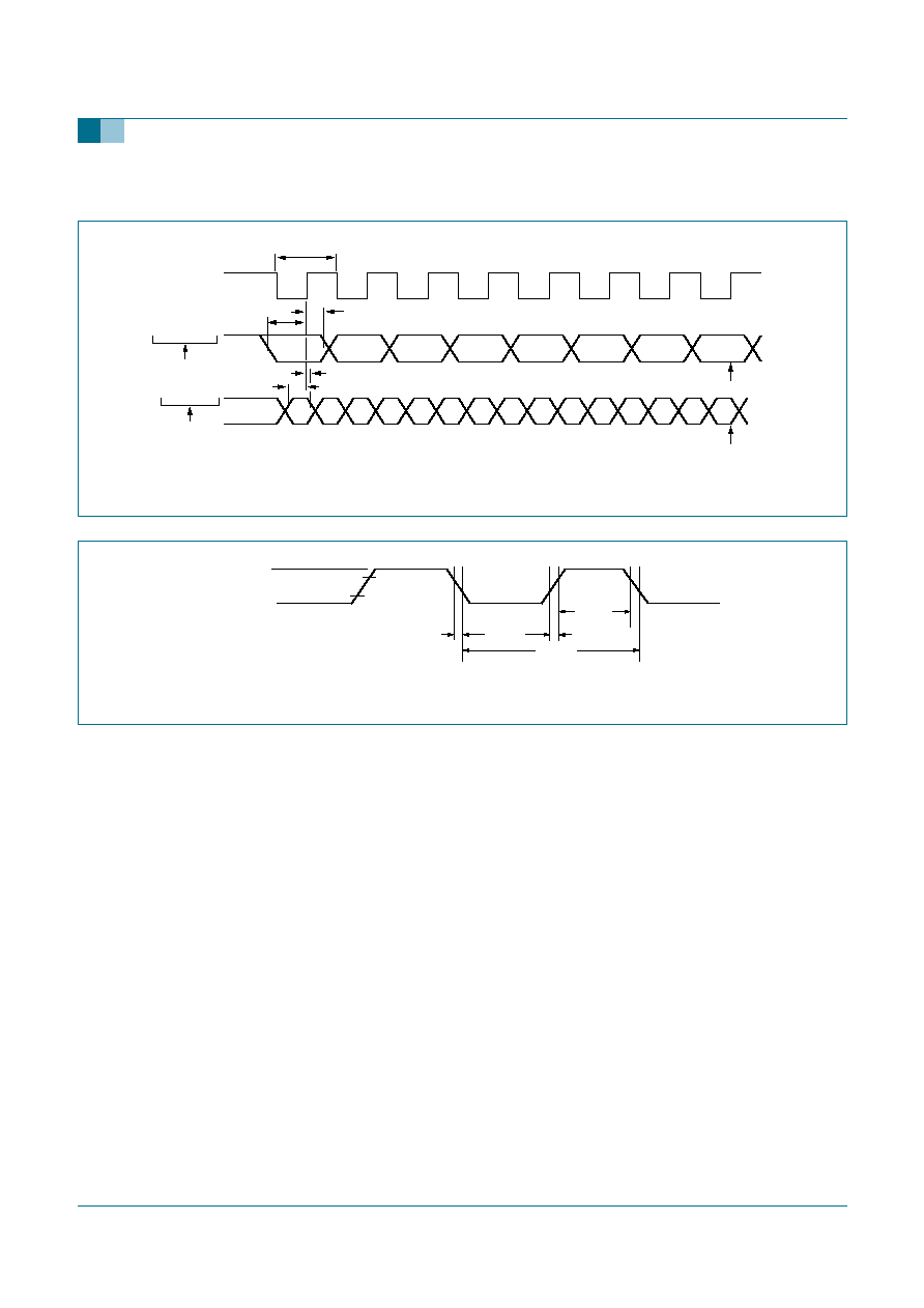
9397 750 14655
� Koninklijke Philips Electronics N.V. 2005. All rights reserved.
Product data sheet
Rev. 02 -- 11 April 2005
51 of 58
Philips Semiconductors
P89LPC9102/9103/9107
8-bit microcontrollers with two-clock accelerated 80C51 core
12.1 Waveforms
Fig 18. Shift register mode timing (P89LPC9103/9107).
0
1
2
3
4
5
6
7
valid
valid
valid
valid
valid
valid
valid
valid
t
XLXL
002aaa981
set TI
set RI
t
XHQX
t
QVXH
t
XHDV
t
XHDX
clock
output data
write to SBUF
input data
clear RI
Fig 19. External clock timing.
t
CHCL
t
CLCX
t
CHCX
T
cy(CLK)
t
CLCH
002aaa907
0.2V
DD
+
0.9 V
0.2V
DD
-
0.1 V
V
DD
-
0.5 V
0.45 V

9397 750 14655
� Koninklijke Philips Electronics N.V. 2005. All rights reserved.
Product data sheet
Rev. 02 -- 11 April 2005
52 of 58
Philips Semiconductors
P89LPC9102/9103/9107
8-bit microcontrollers with two-clock accelerated 80C51 core
13. Other characteristics
13.1 Comparator electrical characteristics
[1]
This parameter is characterized, but not tested in production.
13.2 A/D converter electrical characteristics
Table 15:
Comparator electrical characteristics
V
DD
= 2.4 V to 3.6 V, unless otherwise specified.
T
amb
=
-
40
�
C to +85
�
C for industrial applications, unless otherwise specified.
Symbol
Parameter
Conditions
Min
Typ
Max
Unit
V
IO
offset voltage input voltage
-
-
�
20
mV
V
IC
common mode input voltage
0
-
V
DD
-
0.3
V
CMRR
common mode rejection ratio
[1]
-
-
-
50
dB
t
res(tot)
total response time
-
250
500
ns
t
(CE-OV)
comparator enable to output valid time
-
-
10
�
s
I
LI
input leakage current
0 < V
I
< V
DD
-
-
�
10
�
A
Table 16:
A/D converter electrical characteristics
V
DD
= 2.4 V to 3.6 V, unless otherwise specified.
T
amb
=
-
40
�
C to +85
�
C for industrial applications, unless otherwise specified.
All limits valid for an external source impedance of less than 10 k
.
Symbol
Parameter
Conditions
Min
Typ
Max
Unit
V
IA
analog input voltage
V
SS
-
0.2 -
V
SS
+ 0.2
V
C
iss
analog input capacitance
-
-
15
pF
E
D
differential non-linearity
-
-
�
1
LSB
E
L(adj)
integral non-linearity
-
-
�
1
LSB
E
O
offset error
-
-
�
2
LSB
E
G
gain error
-
-
�
1
%
E
u(tot)
total unadjusted error
-
-
�
2
LSB
M
CTC
channel-to-channel matching
-
-
�
1
LSB
ct(port)
crosstalk between port inputs
0 kHz to 100 kHz
-
-
-
60
dB
SR
in
input slew rate
-
-
100
V/ms
T
cy(ADC)
ADC clock cycle
111
-
2000
ns
t
ADC
conversion time
A/D enabled
-
-
13t
CLK(ADC)
�
s
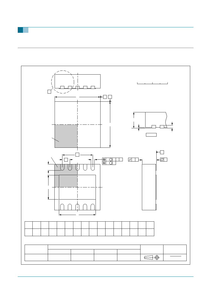
9397 750 14655
� Koninklijke Philips Electronics N.V. 2005. All rights reserved.
Product data sheet
Rev. 02 -- 11 April 2005
53 of 58
Philips Semiconductors
P89LPC9102/9103/9107
8-bit microcontrollers with two-clock accelerated 80C51 core
14. Package outline
Fig 20. Package outline SOT650-1 (HVSON10).
0.5
0.2
1
0.05
0.00
A1
Eh
b
UNIT
D
(1)
y
e
2
e1
REFERENCES
OUTLINE
VERSION
EUROPEAN
PROJECTION
ISSUE DATE
IEC
JEDEC
JEITA
mm
3.1
2.9
c
Dh
1.75
1.45
y1
3.1
2.9
2.55
2.15
0.30
0.18
0.05
0.1
DIMENSIONS (mm are the original dimensions)
SOT650-1
MO-229
- - -
- - -
E
(1)
0.55
0.30
L
0.1
v
0.05
w
0
2 mm
1
scale
SOT650-1
HVSON10: plastic thermal enhanced very thin small outline package; no leads;
10 terminals; body 3 x 3 x 0.85 mm
A
(1)
max.
A
A1
c
detail X
y
Dh
Eh
e
L
10
5
1
6
D
E
y1 C
C
B
A
01-01-22
02-02-08
terminal 1
index area
terminal 1
index area
X
e1
b
A
C
C
B
v
M
w
M
Note
1. Plastic or metal protrusions of 0.075 mm maximum per side are not included.
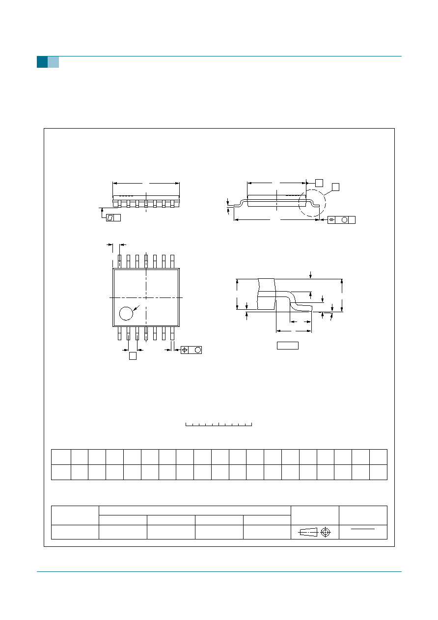
9397 750 14655
� Koninklijke Philips Electronics N.V. 2005. All rights reserved.
Product data sheet
Rev. 02 -- 11 April 2005
54 of 58
Philips Semiconductors
P89LPC9102/9103/9107
8-bit microcontrollers with two-clock accelerated 80C51 core
Fig 21. Package outline SOT402-1 (TSSOP14).
UNIT
A
1
A
2
A
3
b
p
c
D
(1)
E
(2)
(1)
e
H
E
L
L
p
Q
Z
y
w
v
REFERENCES
OUTLINE
VERSION
EUROPEAN
PROJECTION
ISSUE DATE
IEC
JEDEC
JEITA
mm
0.15
0.05
0.95
0.80
0.30
0.19
0.2
0.1
5.1
4.9
4.5
4.3
0.65
6.6
6.2
0.4
0.3
0.72
0.38
8
0
o
o
0.13
0.1
0.2
1
DIMENSIONS (mm are the original dimensions)
Notes
1. Plastic or metal protrusions of 0.15 mm maximum per side are not included.
2. Plastic interlead protrusions of 0.25 mm maximum per side are not included.
0.75
0.50
SOT402-1
MO-153
99-12-27
03-02-18
w
M
b
p
D
Z
e
0.25
1
7
14
8
A
A
1
A
2
L
p
Q
detail X
L
(A )
3
H
E
E
c
v
M
A
X
A
y
0
2.5
5 mm
scale
TSSOP14: plastic thin shrink small outline package; 14 leads; body width 4.4 mm
SOT402-1
A
max.
1.1
pin 1 index

9397 750 14655
� Koninklijke Philips Electronics N.V. 2005. All rights reserved.
Product data sheet
Rev. 02 -- 11 April 2005
55 of 58
Philips Semiconductors
P89LPC9102/9103/9107
8-bit microcontrollers with two-clock accelerated 80C51 core
15. Abbreviations
Table 17:
Acronym list
Acronym
Description
A/D
Analog-to-Digital
BOE
Brownout Enable
CPU
Central Processing Unit
CMRR
Common-Mode Rejection Ratio
DAC
Digital-to-Analog Converter
EMI
Electromagnetic Interference
EPROM
Erasable Programmable Read-Only Memory
HVSON
Heatsink Very thin Small Outline package; No leads
IAP
In-Application Programming
ICP
In-Circuit Programming
LED
Light Emitting Diode
LSB
Least Significant Bit
MSB
Most Significant Bit
PWM
Pulse Width Modulator
RAM
Random Access Memory
RTC
Real-Time Clock
SAR
Successive Approximation Register
TSSOP
Thin Shrink Small Outline Package
UART
Universal Asynchronous Receiver/Transmitter

9397 750 14655
� Koninklijke Philips Electronics N.V. 2005. All rights reserved.
Product data sheet
Rev. 02 -- 11 April 2005
56 of 58
Philips Semiconductors
P89LPC9102/9103/9107
8-bit microcontrollers with two-clock accelerated 80C51 core
16. Revision history
Table 18:
Revision history
Document ID
Release date
Data sheet status
Change notice
Doc. number
Supersedes
P89LPC9102_9103_
9107_2
20050411
Product data sheet
-
9397 750 14655
P89LPC9102_9103
_9107_1
Modifications:
�
Added 18 MHz information.
P89LPC9102_9103_
9107_1
20050111
Product data sheet
-
9397 750 14079
-

Philips Semiconductors
P89LPC9102/9103/9107
8-bit microcontrollers with two-clock accelerated 80C51 core
9397 750 14655
� Koninklijke Philips Electronics N.V. 2005. All rights reserved.
Product data sheet
Rev. 02 -- 11 April 2005
57 of 58
17. Data sheet status
[1]
Please consult the most recently issued data sheet before initiating or completing a design.
[2]
The product status of the device(s) described in this data sheet may have changed since this data sheet was published. The latest information is available on the Internet at
URL http://www.semiconductors.philips.com.
[3]
For data sheets describing multiple type numbers, the highest-level product status determines the data sheet status.
18. Definitions
Short-form specification -- The data in a short-form specification is
extracted from a full data sheet with the same type number and title. For
detailed information see the relevant data sheet or data handbook.
Limiting values definition -- Limiting values given are in accordance with
the Absolute Maximum Rating System (IEC 60134). Stress above one or
more of the limiting values may cause permanent damage to the device.
These are stress ratings only and operation of the device at these or at any
other conditions above those given in the Characteristics sections of the
specification is not implied. Exposure to limiting values for extended periods
may affect device reliability.
Application information -- Applications that are described herein for any
of these products are for illustrative purposes only. Philips Semiconductors
make no representation or warranty that such applications will be suitable for
the specified use without further testing or modification.
19. Disclaimers
Life support -- These products are not designed for use in life support
appliances, devices, or systems where malfunction of these products can
reasonably be expected to result in personal injury. Philips Semiconductors
customers using or selling these products for use in such applications do so
at their own risk and agree to fully indemnify Philips Semiconductors for any
damages resulting from such application.
Right to make changes -- Philips Semiconductors reserves the right to
make changes in the products - including circuits, standard cells, and/or
software - described or contained herein in order to improve design and/or
performance. When the product is in full production (status `Production'),
relevant changes will be communicated via a Customer Product/Process
Change Notification (CPCN). Philips Semiconductors assumes no
responsibility or liability for the use of any of these products, conveys no
license or title under any patent, copyright, or mask work right to these
products, and makes no representations or warranties that these products are
free from patent, copyright, or mask work right infringement, unless otherwise
specified.
20. Contact information
For additional information, please visit: http://www.semiconductors.philips.com
For sales office addresses, send an email to: sales.addresses@www.semiconductors.philips.com
Level
Data sheet status
[1]
Product status
[2] [3]
Definition
I
Objective data
Development
This data sheet contains data from the objective specification for product development. Philips
Semiconductors reserves the right to change the specification in any manner without notice.
II
Preliminary data
Qualification
This data sheet contains data from the preliminary specification. Supplementary data will be published
at a later date. Philips Semiconductors reserves the right to change the specification without notice, in
order to improve the design and supply the best possible product.
III
Product data
Production
This data sheet contains data from the product specification. Philips Semiconductors reserves the
right to make changes at any time in order to improve the design, manufacturing and supply. Relevant
changes will be communicated via a Customer Product/Process Change Notification (CPCN).

� Koninklijke Philips Electronics N.V. 2005
All rights are reserved. Reproduction in whole or in part is prohibited without the prior
written consent of the copyright owner. The information presented in this document does
not form part of any quotation or contract, is believed to be accurate and reliable and may
be changed without notice. No liability will be accepted by the publisher for any
consequence of its use. Publication thereof does not convey nor imply any license under
patent- or other industrial or intellectual property rights.
Date of release: 11 April 2005
Document number: 9397 750 14655
Published in the Netherlands
Philips Semiconductors
P89LPC9102/9103/9107
8-bit microcontrollers with two-clock accelerated 80C51 core
21. Contents
1
General description . . . . . . . . . . . . . . . . . . . . . . 1
2
Features . . . . . . . . . . . . . . . . . . . . . . . . . . . . . . . 1
2.1
Principal features . . . . . . . . . . . . . . . . . . . . . . . 1
2.2
Additional features . . . . . . . . . . . . . . . . . . . . . . 1
3
Product comparison overview . . . . . . . . . . . . . 2
4
Ordering information . . . . . . . . . . . . . . . . . . . . . 3
4.1
Ordering options . . . . . . . . . . . . . . . . . . . . . . . . 3
5
Block diagram . . . . . . . . . . . . . . . . . . . . . . . . . . 4
6
Functional diagram . . . . . . . . . . . . . . . . . . . . . . 6
7
Pinning information . . . . . . . . . . . . . . . . . . . . . . 8
7.1
Pinning . . . . . . . . . . . . . . . . . . . . . . . . . . . . . . . 8
7.2
Pin description . . . . . . . . . . . . . . . . . . . . . . . . . 9
8
Functional description . . . . . . . . . . . . . . . . . . 14
8.1
Special function registers . . . . . . . . . . . . . . . . 14
8.2
Enhanced CPU . . . . . . . . . . . . . . . . . . . . . . . . 26
8.3
Clocks . . . . . . . . . . . . . . . . . . . . . . . . . . . . . . . 26
8.4
On-chip RC oscillator option . . . . . . . . . . . . . . 26
8.5
Watchdog oscillator option . . . . . . . . . . . . . . . 27
8.6
External clock input option . . . . . . . . . . . . . . . 27
8.7
CCLK wake-up delay . . . . . . . . . . . . . . . . . . . 28
8.8
CCLK modification: DIVM register . . . . . . . . . 28
8.9
Low power select . . . . . . . . . . . . . . . . . . . . . . 28
8.10
Memory organization . . . . . . . . . . . . . . . . . . . 28
8.11
Interrupts . . . . . . . . . . . . . . . . . . . . . . . . . . . . 28
8.12
I/O ports . . . . . . . . . . . . . . . . . . . . . . . . . . . . . 30
8.13
Power monitoring functions. . . . . . . . . . . . . . . 32
8.14
Power reduction modes . . . . . . . . . . . . . . . . . 32
8.15
Reset . . . . . . . . . . . . . . . . . . . . . . . . . . . . . . . 33
8.16
Timers 0 and 1 . . . . . . . . . . . . . . . . . . . . . . . . 34
8.17
RTC/system timer . . . . . . . . . . . . . . . . . . . . . . 35
8.18
UART (P89LPC9103/9107) . . . . . . . . . . . . . . 35
8.19
Analog comparators . . . . . . . . . . . . . . . . . . . . 37
8.20
Internal reference voltage . . . . . . . . . . . . . . . . 37
8.21
Comparator interrupt. . . . . . . . . . . . . . . . . . . . 38
8.22
Comparator and power reduction modes . . . . 38
8.23
Keypad interrupt (KBI) . . . . . . . . . . . . . . . . . . 38
8.24
Watchdog timer. . . . . . . . . . . . . . . . . . . . . . . . 38
8.25
Additional features . . . . . . . . . . . . . . . . . . . . . 39
8.26
Flash program memory. . . . . . . . . . . . . . . . . . 40
9
A/D Converter. . . . . . . . . . . . . . . . . . . . . . . . . . 42
9.1
General description. . . . . . . . . . . . . . . . . . . . . 42
9.2
Features . . . . . . . . . . . . . . . . . . . . . . . . . . . . . 42
9.3
Block diagram . . . . . . . . . . . . . . . . . . . . . . . . . 43
9.4
A/D operating modes . . . . . . . . . . . . . . . . . . . 43
9.5
Conversion start modes . . . . . . . . . . . . . . . . . 44
9.6
Boundary limits interrupt. . . . . . . . . . . . . . . . . 44
9.7
DAC output to a port pin with high output
impedance . . . . . . . . . . . . . . . . . . . . . . . . . . . 44
9.8
Clock divider. . . . . . . . . . . . . . . . . . . . . . . . . . 44
9.9
Power-down and Idle mode . . . . . . . . . . . . . . 45
10
Limiting values . . . . . . . . . . . . . . . . . . . . . . . . 46
11
Static characteristics . . . . . . . . . . . . . . . . . . . 47
12
Dynamic characteristics . . . . . . . . . . . . . . . . . 49
12.1
Waveforms . . . . . . . . . . . . . . . . . . . . . . . . . . . 51
13
Other characteristics . . . . . . . . . . . . . . . . . . . 52
13.1
Comparator electrical characteristics . . . . . . . 52
13.2
A/D converter electrical characteristics . . . . . 52
14
Package outline . . . . . . . . . . . . . . . . . . . . . . . . 53
15
Abbreviations . . . . . . . . . . . . . . . . . . . . . . . . . 55
16
Revision history . . . . . . . . . . . . . . . . . . . . . . . 56
17
Data sheet status. . . . . . . . . . . . . . . . . . . . . . . 57
18
Definitions . . . . . . . . . . . . . . . . . . . . . . . . . . . . 57
19
Disclaimers . . . . . . . . . . . . . . . . . . . . . . . . . . . 57
20
Contact information . . . . . . . . . . . . . . . . . . . . 57