
1.
General description
The PCA9546A is a quad bi-directional translating switch controlled via the I
2
C-bus. The
SCL/SDA upstream pair fans out to four downstream pairs, or channels. Any individual
SCx/SDx channel or combination of channels can be selected, determined by the
contents of the programmable control register.
An active LOW reset input allows the PCA9546A to recover from a situation where one of
the downstream I
2
C-buses is stuck in a LOW state. Pulling the RESET pin LOW resets the
I
2
C-bus state machine and causes all the channels to be deselected as does the internal
Power-On Reset (POR) function.
The pass gates of the switches are constructed such that the V
DD
pin can be used to limit
the maximum high voltage which will be passed by the PCA9546A. This allows the use of
different bus voltages on each pair, so that 1.8 V or 2.5 V or 3.3 V parts can communicate
with 5 V parts without any additional protection. External pull-up resistors pull the bus up
to the desired voltage level for each channel. All I/O pins are 5 V tolerant.
2.
Features
s
1-of-4 bi-directional translating switches
s
I
2
C-bus interface logic; compatible with SMBus standards
s
Active LOW reset input
s
3 address pins allowing up to 8 devices on the I
2
C-bus
s
Channel selection via I
2
C-bus, in any combination
s
Power-up with all switch channels deselected
s
Low R
on
switches
s
Allows voltage level translation between 1.8 V, 2.5 V, 3.3 V and 5 V buses
s
No glitch on power-up
s
Supports hot insertion
s
Low stand-by current
s
Operating power supply voltage range of 2.3 V to 5.5 V
s
5 V tolerant Inputs
s
0 kHz to 400 kHz clock frequency
s
ESD protection exceeds 2000 V HBM per JESD22-A114, 200 V MM per
JESD22-A115, and 1000 V CDM per JESD22-C101
s
Latch-up testing is done to JEDEC Standard JESD78 which exceeds 100 mA
s
Three packages offered: SO16, TSSOP16, and HVQFN16
PCA9546A
4-channel I
2
C switch with reset
Rev. 03 -- 6 April 2005
Product data sheet

9397 750 14318
� Koninklijke Philips Electronics N.V. 2005. All rights reserved.
Product data sheet
Rev. 03 -- 6 April 2005
2 of 25
Philips Semiconductors
PCA9546A
4-channel I
2
C switch with reset
3.
Ordering information
Standard packing quantities and other packaging data are available at
www.standardics.philips.com/packaging.
4.
Marking
Table 1:
Ordering information
T
amb
=
-
40
�
C to +85
�
C
Type number
Package
Name
Description
Version
PCA9546ABS
HVQFN16
plastic thermal enhanced very thin quad flat package;
no leads; 16 terminals; body 4
�
4
�
0.85 mm
SOT629-1
PCA9546AD
SO16
plastic small outline package; 16 leads;
body width 3.9 mm
SOT109-1
PCA9546APW
TSSOP16
plastic thin shrink small outline package; 16 leads;
body width 4.4 mm
SOT403-1
Table 2:
Marking codes
Type number
Topside mark
PCA9546ABS
546A
PCA9546AD
PCA9546AD
PCA9546APW
PA9546A
9397 750 14318
� Koninklijke Philips Electronics N.V. 2005. All rights reserved.
Product data sheet
Rev. 03 -- 6 April 2005
3 of 25
Philips Semiconductors
PCA9546A
4-channel I
2
C switch with reset
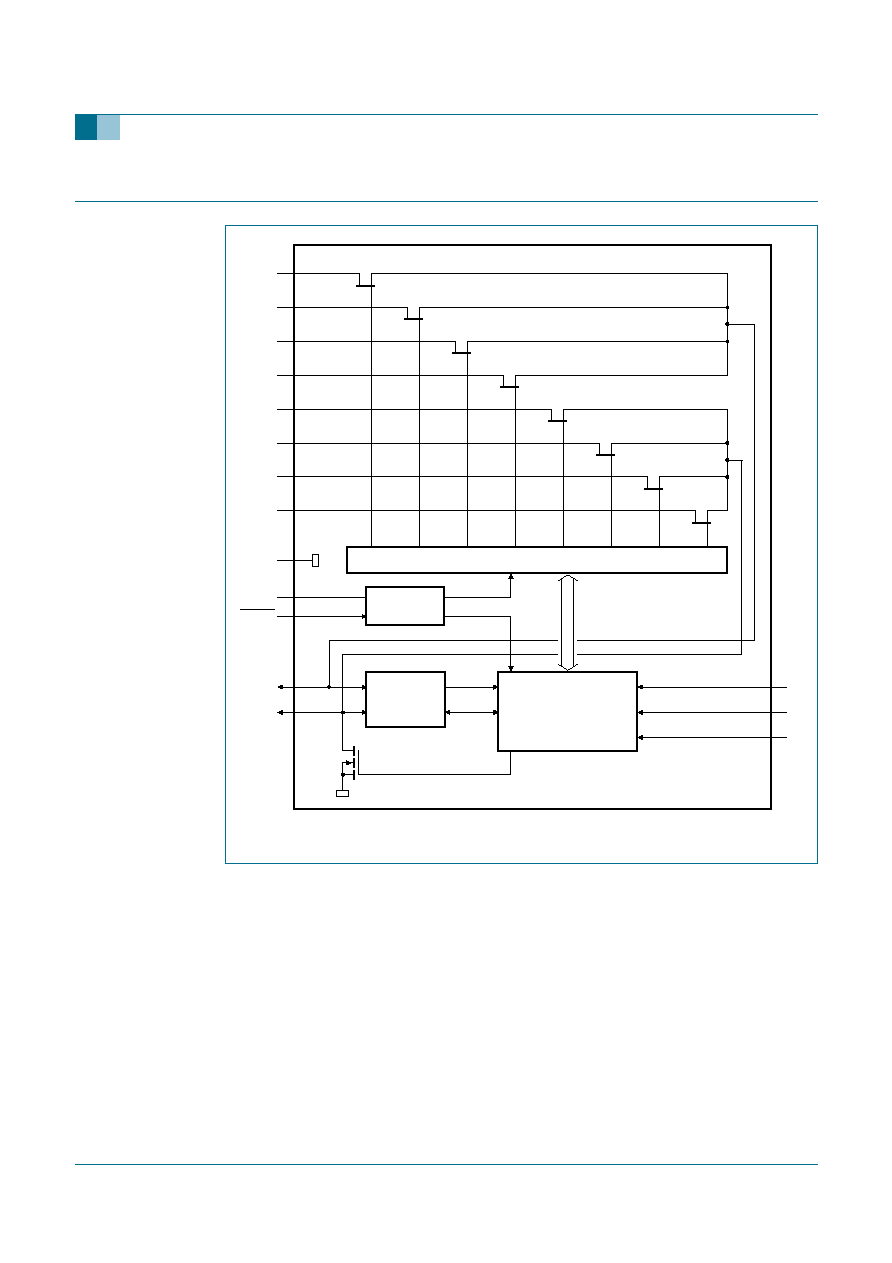
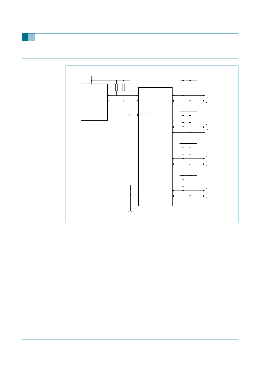
5.
Block diagram
Fig 1.
Block diagram of PCA9546A
SWITCH CONTROL LOGIC
PCA9546A
POWER-ON
RESET
002aab188
SC0
SC1
SC2
SC3
SD0
SD1
SD2
SD3
V
SS
V
DD
RESET
I
2
C-BUS
CONTROL
INPUT
FILTER
SCL
SDA
A0
A1
A2
9397 750 14318
� Koninklijke Philips Electronics N.V. 2005. All rights reserved.
Product data sheet
Rev. 03 -- 6 April 2005
4 of 25
Philips Semiconductors
PCA9546A
4-channel I
2
C switch with reset
6.
Pinning information
6.1 Pinning
Fig 2.
Pin configuration for SO16
Fig 3.
Pin configuration for TSSOP16
Fig 4.
Pin configuration for HVQFN16 (transparent top view)
PCA9546AD
A0
V
DD
A1
SDA
RESET
SCL
SD0
A2
SC0
SC3
SD1
SD3
SC1
SC2
V
SS
SD2
002aab185
1
2
3
4
5
6
7
8
10
9
12
11
14
13
16
15
PCA9546APW
A0
V
DD
A1
SDA
RESET
SCL
SD0
A2
SC0
SC3
SD1
SD3
SC1
SC2
V
SS
SD2
002aab186
1
2
3
4
5
6
7
8
10
9
12
11
14
13
16
15
002aab187
Transparent top view
SD1
SD3
SC0
SC3
SD0
A2
RESET
SCL
SC1
V
SS
SD2
SC2
A1
A0
V
DD
SDA
4
9
3
10
2
11
1
12
5
6
7
8
16
15
14
13
terminal 1
index area
PCA9546ABS
9397 750 14318
� Koninklijke Philips Electronics N.V. 2005. All rights reserved.
Product data sheet
Rev. 03 -- 6 April 2005
5 of 25
Philips Semiconductors
PCA9546A
4-channel I
2
C switch with reset
6.2 Pin description
[1]
HVQFN package die supply ground is connected to both the V
SS
pin and the exposed center pad. The V
SS
pin must be connected to supply ground for proper device operation. For enhanced thermal, electrical, and
board-level performance, the exposed pad needs to be soldered to the board using a corresponding
thermal pad on the board, and for proper heat conduction through the board thermal vias need to be
incorporated in the PCB in the thermal pad region.
7.
Functional description
Refer to
Figure 1 "Block diagram of PCA9546A" on page 3
.
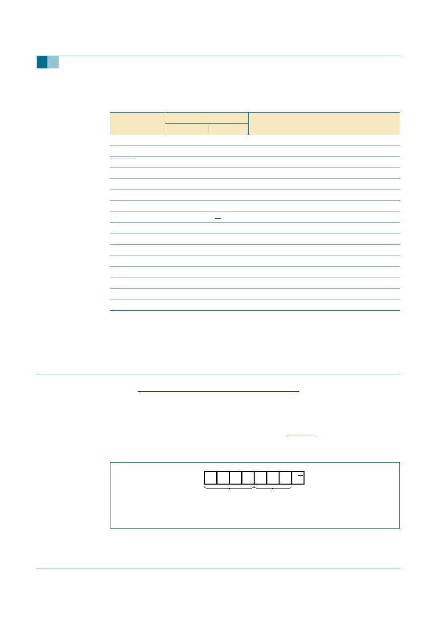
7.1 Device address
Following a START condition, the bus master must output the address of the slave it is
accessing. The address of the PCA9546A is shown in
Figure 5
. To conserve power, no
internal pull-up resistors are incorporated on the hardware selectable address pins and
they must be pulled HIGH or LOW.
The last bit of the slave address defines the operation to be performed. When set to
logic 1 a read is selected, while a logic 0 selects a write operation.
Table 3:
Pin description
Symbol
Pin
Description
SO, TSSOP
HVQFN
A0
1
15
address input 0
A1
2
16
address input 1
RESET
3
1
active LOW reset input
SD0
4
2
serial data 0
SC0
5
3
serial clock 0
SD1
6
4
serial data 1
SC1
7
5
serial clock 1
V
SS
8
6
[1]
supply ground
SD2
9
7
serial data 2
SC2
10
8
serial clock 2
SD3
11
9
serial data 3
SC3
12
10
serial clock 3
A2
13
11
address input 2
SCL
14
12
serial clock line
SDA
15
13
serial data line
V
DD
16
14
supply voltage
Fig 5.
Slave address
002aab189
1
1
1
0
A2
A1
A0 R/W
fixed
hardware
selectable
9397 750 14318
� Koninklijke Philips Electronics N.V. 2005. All rights reserved.
Product data sheet
Rev. 03 -- 6 April 2005
6 of 25
Philips Semiconductors
PCA9546A
4-channel I
2
C switch with reset
7.2 Control register
Following the successful acknowledgement of the slave address, the bus master will send
a byte to the PCA9546A, which will be stored in the control register. If multiple bytes are
received by the PCA9546A, it will save the last byte received. This register can be written
and read via the I
2
C-bus.
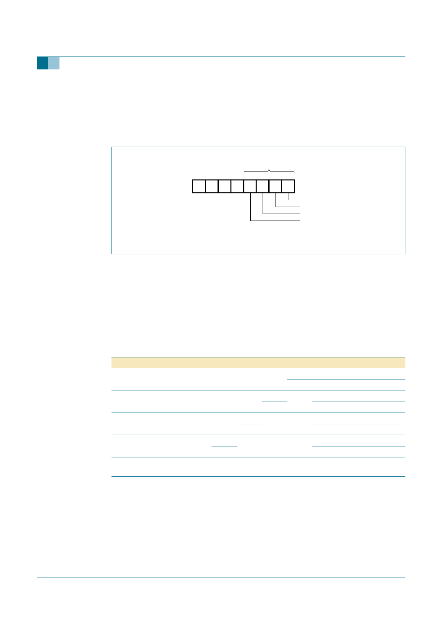
7.2.1 Control register definition
One or several SCx/SDx downstream pair, or channel, is selected by the contents of the
control register. This register is written after the PCA9546A has been addressed. The
4 LSBs of the control byte are used to determine which channel is to be selected. When a
channel is selected, the channel will become active after a STOP condition has been
placed on the I
2
C-bus. This ensures that all SCx/SDx lines will be in a HIGH state when
the channel is made active, so that no false conditions are generated at the time of
connection.
Remark: Several channels can be enabled at the same time. Example: B3 = 0, B2 = 1,
B1 = 1, B0 = 0, means that channel 0 and channel 3 are disabled and channel 1 and
channel 2 are enabled. Care should be taken not to exceed the maximum bus
capacitance.
Fig 6.
Control register
002aab190
X
X
X
X
B3
B2
B1
B0
channel selection bits
(read/write)
7
6
5
4
3
2
1
0
channel 0
channel 1
channel 2
channel 3
Table 4:
Control register: Write--channel selection; Read--channel status
D7
D6
D5
D4
B3
B2
B1
B0
Command
X
X
X
X
X
X
X
0
channel 0 disabled
1
channel 0 enabled
X
X
X
X
X
X
0
X
channel 1 disabled
1
channel 1 enabled
X
X
X
X
X
0
X
X
channel 2 disabled
1
channel 2 enabled
X
X
X
X
0
X
X
X
channel 3 disabled
1
channel 3 enabled
0
0
0
0
0
0
0
0
no channel selected;
power-up/reset default state
9397 750 14318
� Koninklijke Philips Electronics N.V. 2005. All rights reserved.
Product data sheet
Rev. 03 -- 6 April 2005
7 of 25
Philips Semiconductors
PCA9546A
4-channel I
2
C switch with reset
7.3 RESET input
The RESET input is an active LOW signal which may be used to recover from a bus fault
condition. By asserting this signal LOW for a minimum of t
WL
, the PCA9546A will reset its
registers and I
2
C-bus state machine and will deselect all channels. The RESET input must
be connected to V
DD
through a pull-up resistor.
7.4 Power-on reset
When power is applied to V
DD
, an internal Power-On Reset (POR) holds the PCA9546A in
a reset condition until V
DD
has reached V
POR
. At this point, the reset condition is released
and the PCA9546A registers and I
2
C-bus state machine are initialized to their default
states--all zeroes--causing all the channels to be deselected. Thereafter, V
DD
must be
lowered below 0.2 V to reset the device.
7.5 Voltage translation
The pass gate transistors of the PCA9546A are constructed such that the V
DD
voltage can
be used to limit the maximum voltage that will be passed from one I
2
C-bus to another.
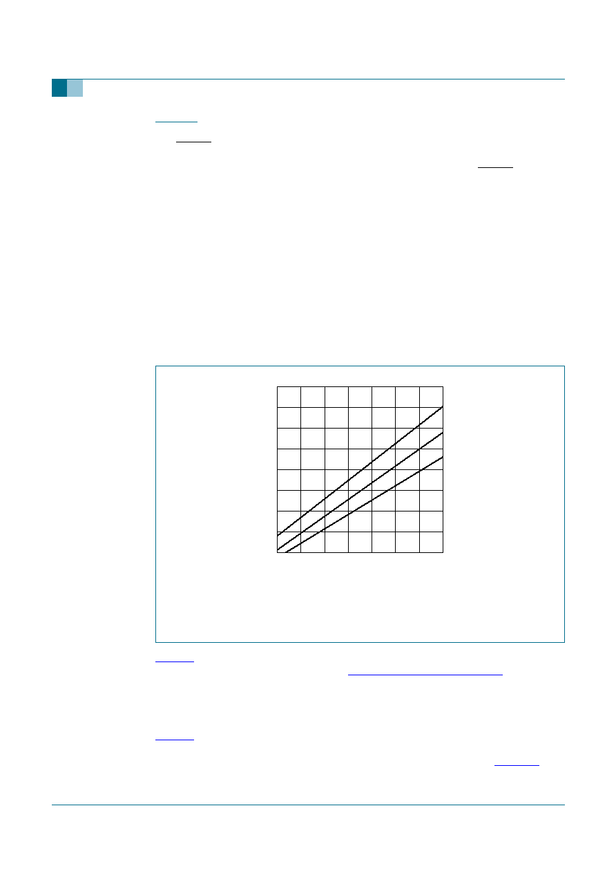
Figure 7
shows the voltage characteristics of the pass gate transistors (note that the graph
was generated using the data specified in
Section 11 "Static characteristics"
of this data
sheet). In order for the PCA9546A to act as a voltage translator, the V
o(sw)
voltage should
be equal to, or lower than the lowest bus voltage. For example, if the main bus was
running at 5 V, and the downstream buses were 3.3 V and 2.7 V, then V
o(sw)
should be
equal to or below 2.7 V to effectively clamp the downstream bus voltages. Looking at
Figure 7
, we see that V
o(sw)(max)
will be at 2.7 V when the PCA9546A supply voltage is
3.5 V or lower, so the PCA9546A supply voltage could be set to 3.3 V. Pull-up resistors
can then be used to bring the bus voltages to their appropriate levels (see
Figure 14
).
(1) maximum
(2) typical
(3) minimum
Fig 7.
Pass gate voltage versus supply voltage
V
DD
(V)
2.0
5.5
4.5
3.0
4.0
002aaa964
3.0
2.0
4.0
5.0
V
o(sw)
(V)
1.0
3.5
5.0
2.5
(1)
(2)
(3)
9397 750 14318
� Koninklijke Philips Electronics N.V. 2005. All rights reserved.
Product data sheet
Rev. 03 -- 6 April 2005
8 of 25
Philips Semiconductors
PCA9546A
4-channel I
2
C switch with reset
More Information can be found in Application Note
AN262: PCA954X family of I2C/SMBus
multiplexers and switches.
8.
Characteristics of the I
2
C-bus
The I
2
C-bus is for 2-way, 2-line communication between different ICs or modules. The two
lines are a serial data line (SDA) and a serial clock line (SCL). Both lines must be
connected to a positive supply via a pull-up resistor when connected to the output stages
of a device. Data transfer may be initiated only when the bus is not busy.
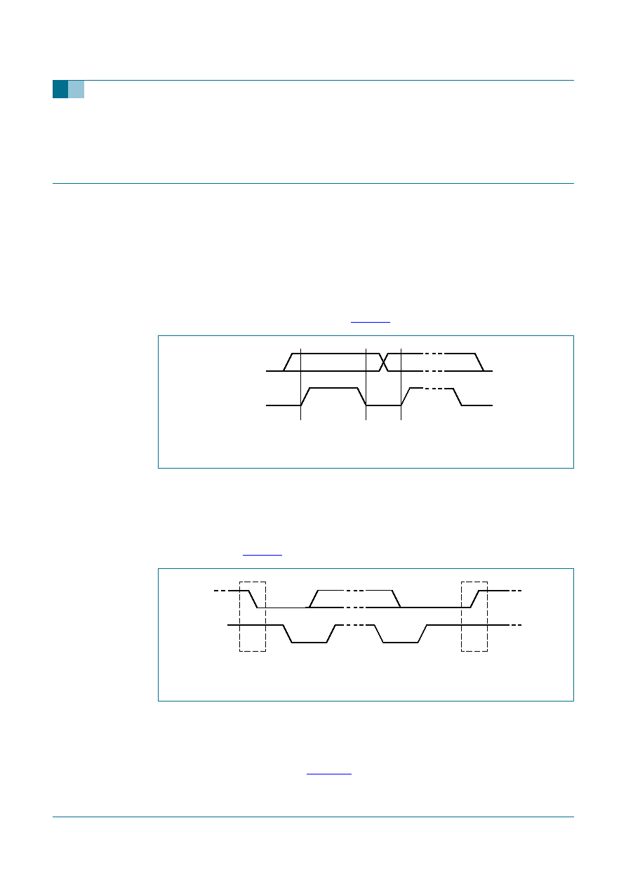
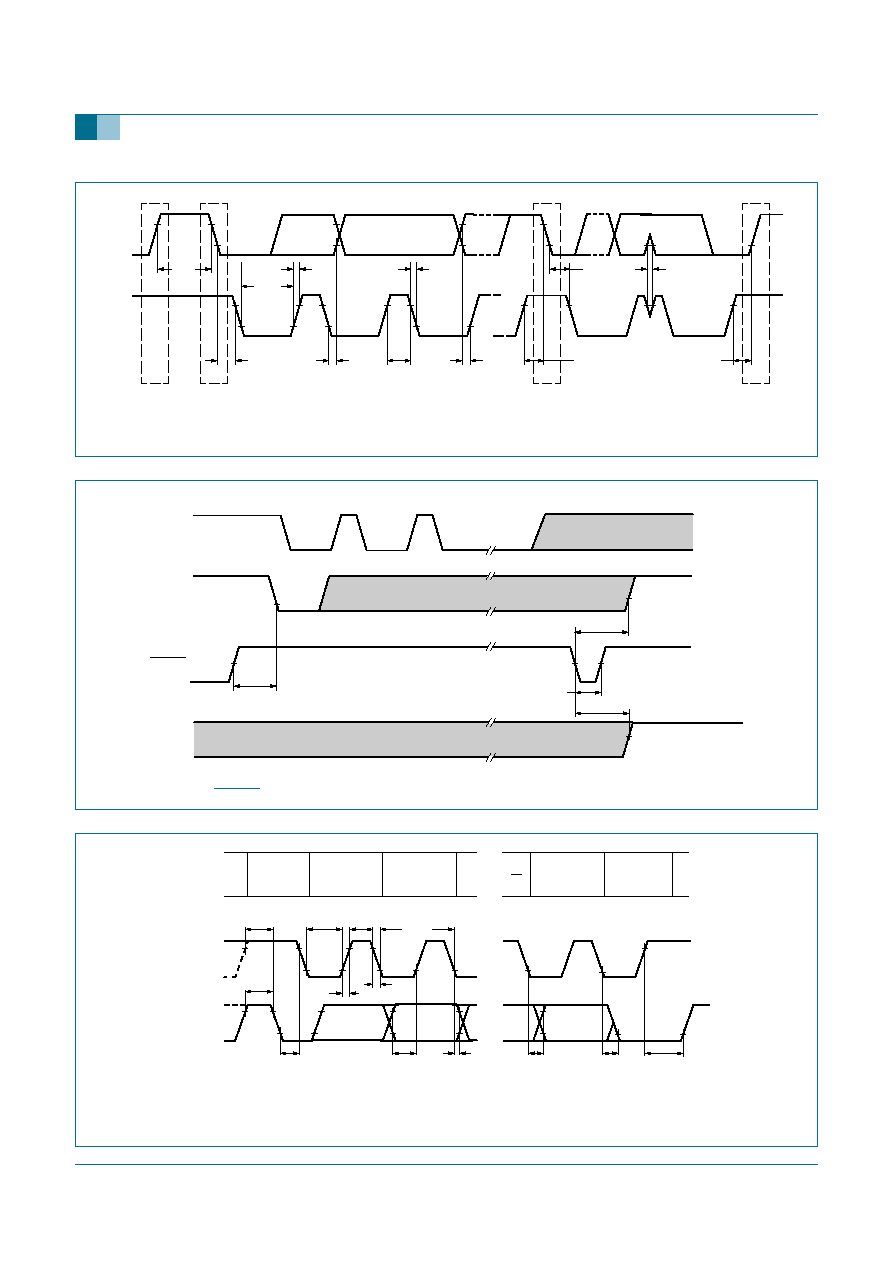
8.1 Bit transfer
One data bit is transferred during each clock pulse. The data on the SDA line must remain
stable during the HIGH period of the clock pulse as changes in the data line at this time
will be interpreted as control signals (see
Figure 8
).
8.2 START and STOP conditions
Both data and clock lines remain HIGH when the bus is not busy. A HIGH-to-LOW
transition of the data line while the clock is HIGH is defined as the START condition (S).
A LOW-to-HIGH transition of the data line while the clock is HIGH is defined as the STOP
condition (P) (see
Figure 9
).
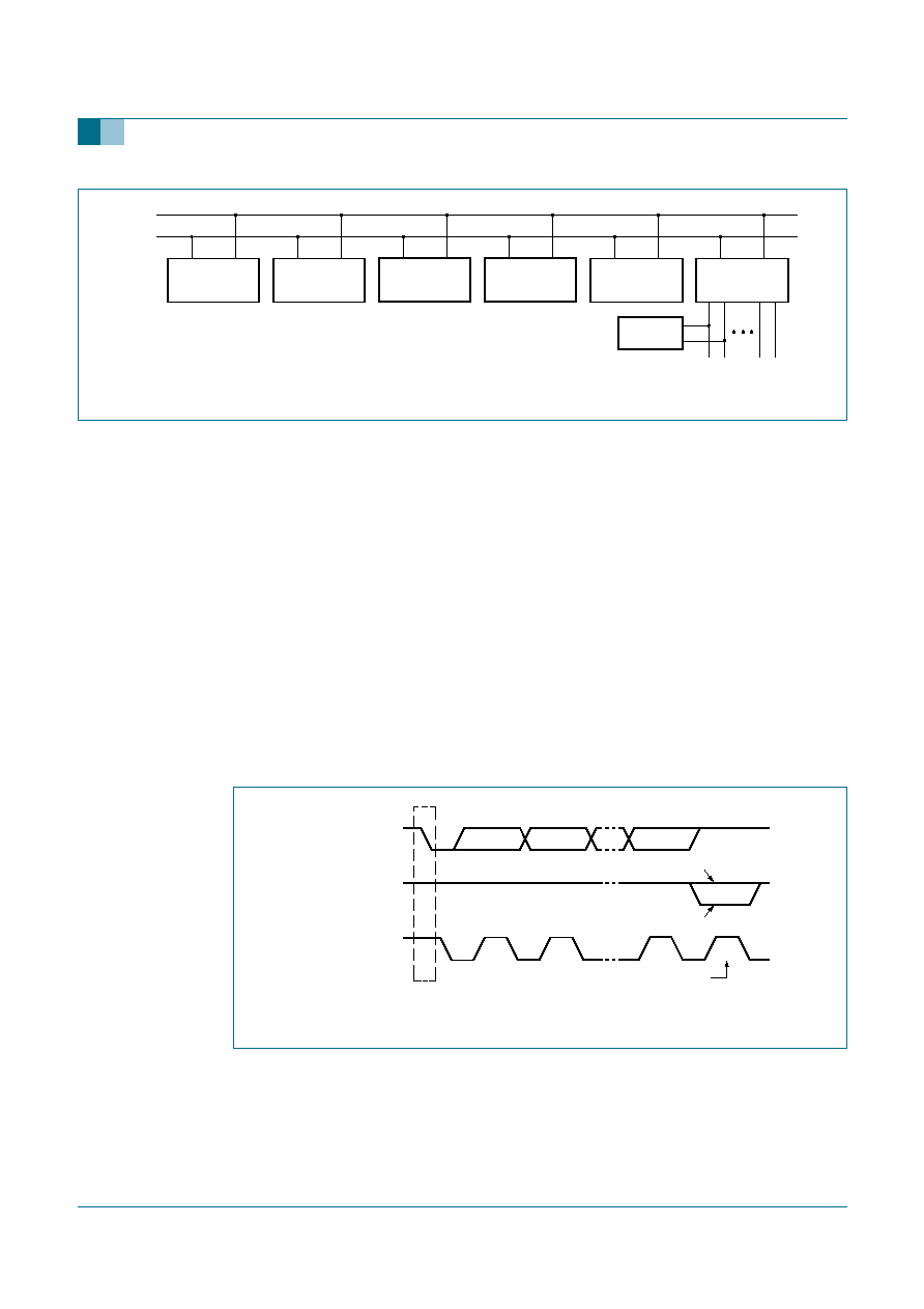
8.3 System configuration
A device generating a message is a `transmitter', a device receiving is the `receiver'. The
device that controls the message is the `master' and the devices which are controlled by
the master are the `slaves' (see
Figure 10
).
Fig 8.
Bit transfer
mba607
data line
stable;
data valid
change
of data
allowed
SDA
SCL
Fig 9.
Definition of START and STOP conditions
mba608
SDA
SCL
P
STOP condition
SDA
SCL
S
START condition
9397 750 14318
� Koninklijke Philips Electronics N.V. 2005. All rights reserved.
Product data sheet
Rev. 03 -- 6 April 2005
9 of 25
Philips Semiconductors
PCA9546A
4-channel I
2
C switch with reset
8.4 Acknowledge
The number of data bytes transferred between the START and the STOP conditions from
transmitter to receiver is not limited. Each byte of eight bits is followed by one
acknowledge bit. The acknowledge bit is a HIGH level put on the bus by the transmitter,
whereas the master generates an extra acknowledge related clock pulse.
A slave receiver which is addressed must generate an acknowledge after the reception of
each byte. Also, a master must generate an acknowledge after the reception of each byte
that has been clocked out of the slave transmitter. The device that acknowledges has to
pull down the SDA line during the acknowledge clock pulse so that the SDA line is stable
LOW during the HIGH period of the acknowledge related clock pulse; setup and hold
times must be taken into account.
A master receiver must signal an end of data to the transmitter by not generating an
acknowledge on the last byte that has been clocked out of the slave. In this event, the
transmitter must leave the data line HIGH to enable the master to generate a STOP
condition.
Fig 10. System configuration
002aaa966
MASTER
TRANSMITTER/
RECEIVER
SLAVE
RECEIVER
SLAVE
TRANSMITTER/
RECEIVER
MASTER
TRANSMITTER
MASTER
TRANSMITTER/
RECEIVER
SDA
SCL
I
2
C
MULTIPLEXER
SLAVE
Fig 11. Acknowledgement on the I
2
C-bus
002aaa987
S
START
condition
9
8
2
1
clock pulse for
acknowledgement
not acknowledge
acknowledge
data output
by transmitter
data output
by receiver
SCL from master
9397 750 14318
� Koninklijke Philips Electronics N.V. 2005. All rights reserved.
Product data sheet
Rev. 03 -- 6 April 2005
10 of 25
Philips Semiconductors
PCA9546A
4-channel I
2
C switch with reset
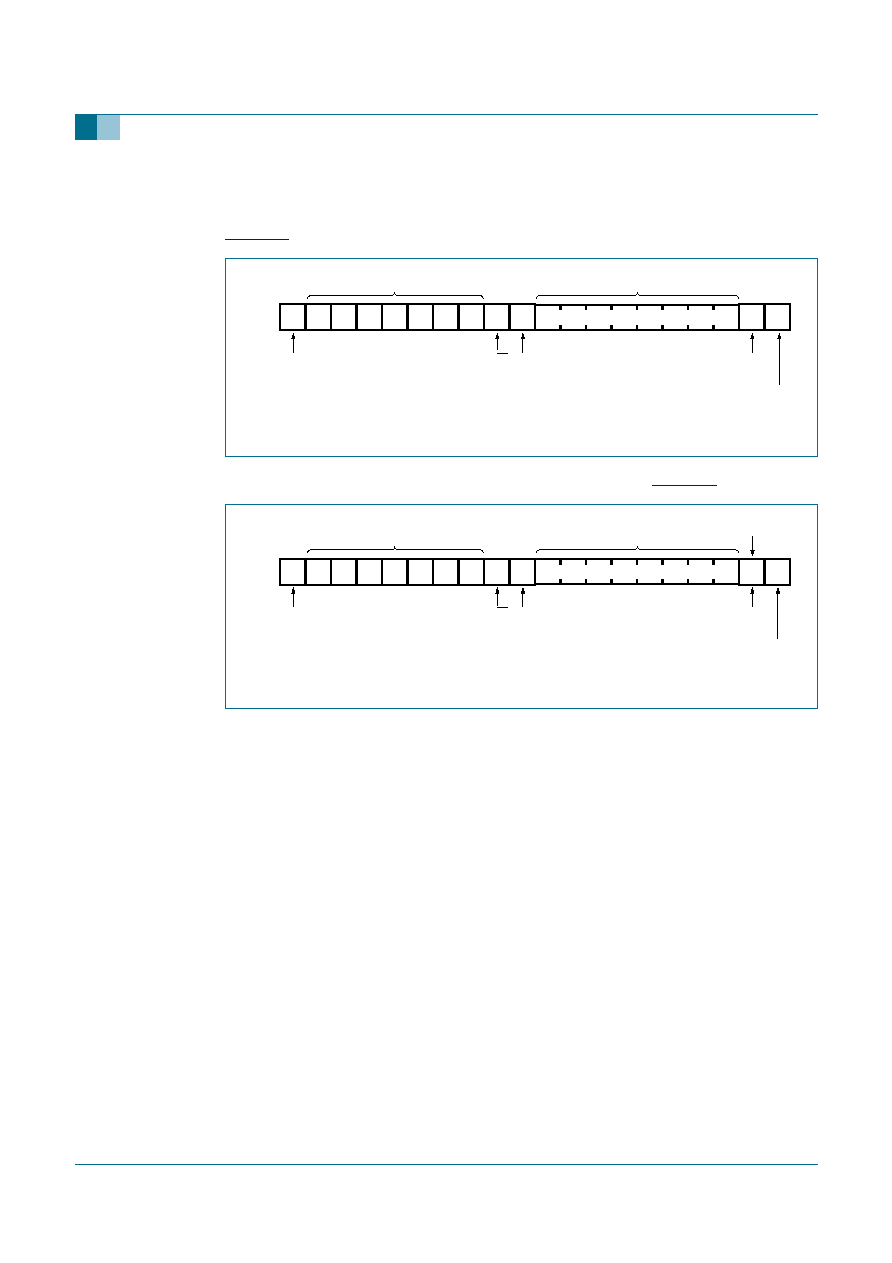
8.5 Bus transactions
Data is transmitted to the PCA9546A control register using the Write mode as shown in
Figure 12
.
Data is read from PCA9546A using the Read mode as shown in
Figure 13
.
Fig 12. Write control register
Fig 13. Read control register
002aab196
X
X
X
X
B3
B2
B1
B0
1
1
0
A2
A1
A0
0
A
S
1
A
P
slave address
START condition
R/W
acknowledge
from slave
acknowledge
from slave
control register
SDA
STOP condition
002aab197
X
X
X
X
B3
B2
B1
B0
1
1
0
A2
A1
A0
1
A
S
1
NA
P
slave address
START condition
R/W
acknowledge
from slave
no acknowledge
from master
control register
SDA
STOP condition
last byte
9397 750 14318
� Koninklijke Philips Electronics N.V. 2005. All rights reserved.
Product data sheet
Rev. 03 -- 6 April 2005
11 of 25
Philips Semiconductors
PCA9546A
4-channel I
2
C switch with reset
9.
Application design-in information
Fig 14. Typical application
PCA9546A
SD0
SC0
A1
A0
V
SS
SDA
SCL
RESET
V
DD
= 3.3 V
V
DD
= 2.7 V to 5.5 V
I
2
C/SMBus master
002aab198
SDA
SCL
channel 0
V = 2.7 V to 5.5 V
SD1
SC1
channel 1
V = 2.7 V to 5.5 V
SD2
SC2
channel 2
V = 2.7 V to 5.5 V
SD3
SC3
channel 3
V = 2.7 V to 5.5 V
A2

9397 750 14318
� Koninklijke Philips Electronics N.V. 2005. All rights reserved.
Product data sheet
Rev. 03 -- 6 April 2005
12 of 25
Philips Semiconductors
PCA9546A
4-channel I
2
C switch with reset
10. Limiting values
[1]
The performance capability of a high-performance integrated circuit in conjunction with its thermal
environment can create junction temperatures which are detrimental to reliability. The maximum junction
temperature of this integrated circuit should not exceed 150
�
C.
Table 5:
Limiting values
In accordance with the Absolute Maximum Rating System (IEC 60134).
Voltages are referenced to V
SS
(ground = 0 V).
[1]
Symbol
Parameter
Conditions
Min
Max
Unit
V
DD
supply voltage
-
0.5
+7.0
V
V
I
input voltage
-
0.5
+7.0
V
I
I
input current
-
�
20
mA
I
O
output current
-
�
25
mA
I
DD
supply current
-
�
100
mA
I
SS
ground supply current
-
�
100
mA
P
tot
total power dissipation
-
400
mW
T
stg
storage temperature
-
60
+150
�
C
T
amb
operating ambient temperature
-
40
+85
�
C

9397 750 14318
� Koninklijke Philips Electronics N.V. 2005. All rights reserved.
Product data sheet
Rev. 03 -- 6 April 2005
13 of 25
Philips Semiconductors
PCA9546A
4-channel I
2
C switch with reset
11. Static characteristics
[1]
For operation between published voltage ranges, refer to the worst-case parameter in both ranges.
[2]
V
DD
must be lowered to 0.2 V in order to reset part.
Table 6:
DC characteristics
V
DD
= 2.3 V to 3.6 V; V
SS
= 0 V; T
amb
=
-
40
�
C to +85
�
C; unless otherwise specified.
See
Table 7 on page 14
for V
DD
= 4.5 V to 5.5 V.
[1]
Symbol
Parameter
Conditions
Min
Typ
Max
Unit
Supply
V
DD
supply voltage
2.3
-
3.6
V
I
DD
supply current
Operating mode; V
DD
= 3.6 V; no load;
V
I
= V
DD
or V
SS
; f
SCL
= 100 kHz
-
16
50
�
A
I
stb
standby current
Standby mode; V
DD
= 3.6 V; no load;
V
I
= V
DD
or V
SS
-
0.1
1
�
A
V
POR
power-on reset voltage
no load; V
I
= V
DD
or V
SS
[2]
-
1.6
2.1
V
Input SCL; input/output SDA
V
IL
LOW-level input voltage
-
0.5
-
0.3V
DD
V
V
IH
HIGH-level input voltage
0.7V
DD
-
6
V
I
OL
LOW-level output current
V
OL
= 0.4 V
3
-
-
mA
V
OL
= 0.6 V
6
-
-
mA
I
L
leakage current
V
I
= V
DD
or V
SS
-
1
-
+1
�
A
C
i
input capacitance
V
I
= V
SS
-
12
13
pF
Select inputs A0 to A2, RESET
V
IL
LOW-level input voltage
-
0.5
-
0.3V
DD
V
V
IH
HIGH-level input voltage
0.7V
DD
-
V
DD
+ 0.5
V
I
LI
input leakage current
pin at V
DD
or V
SS
-
1
-
+1
�
A
C
i
input capacitance
V
I
= V
SS
-
1.6
3
pF
Pass gate
R
on
on-state resistance
V
DD
= 3.67 V; V
O
= 0.4 V; I
O
= 15 mA
5
11
30
V
DD
= 2.3 V to 2.7 V; V
O
= 0.4 V;
I
O
= 10 mA
7
16
55
V
o(sw)
switch output voltage
V
i(sw)
= V
DD
= 3.3 V; I
o(sw)
=
-
100
�
A
-
1.9
-
V
V
i(sw)
= V
DD
= 3.0 V to 3.6 V;
I
o(sw)
=
-
100
�
A
1.6
-
2.8
V
V
i(sw)
= V
DD
= 2.5 V; I
o(sw)
=
-
100
�
A
-
1.5
-
V
V
i(sw)
= V
DD
= 2.3 V to 2.7 V;
I
o(sw)
=
-
100
�
A
1.1
-
2.0
V
I
L
leakage current
V
I
= V
DD
or V
SS
-
1
-
+1
�
A
C
io
input/output capacitance
V
I
= V
SS
-
3
5
pF

9397 750 14318
� Koninklijke Philips Electronics N.V. 2005. All rights reserved.
Product data sheet
Rev. 03 -- 6 April 2005
14 of 25
Philips Semiconductors
PCA9546A
4-channel I
2
C switch with reset
[1]
For operation between published voltage ranges, refer to the worst-case parameter in both ranges.
[2]
V
DD
must be lowered to 0.2 V in order to reset part.
Table 7:
DC characteristics
V
DD
= 4.5 V to 5.5 V; V
SS
= 0 V; T
amb
=
-
40
�
C to +85
�
C; unless otherwise specified.
See
Table 6 on page 13
for V
DD
= 2.3 V to 3.6 V.
[1]
Symbol
Parameter
Conditions
Min
Typ
Max
Unit
Supply
V
DD
supply voltage
4.5
-
5.5
V
I
DD
supply current
Operating mode; V
DD
= 5.5 V;
no load; V
I
= V
DD
or V
SS
;
f
SCL
= 100 kHz
-
65
100
�
A
I
stb
standby current
Standby mode; V
DD
= 5.5 V;
no load; V
I
= V
DD
or V
SS
-
0.3
1
�
A
V
POR
power-on reset voltage
no load; V
I
= V
DD
or V
SS
[2]
-
1.7
2.1
V
Input SCL; input/output SDA
V
IL
LOW-level input voltage
-
0.5
-
0.3V
DD
V
V
IH
HIGH-level input voltage
0.7V
DD
-
6
V
I
OL
LOW-level output current
V
OL
= 0.4 V
3
-
-
mA
V
OL
= 0.6 V
6
-
-
mA
I
IL
LOW-level input current
V
I
= V
SS
1
-
1
�
A
I
IH
HIGH-level input current
V
I
= V
DD
1
-
1
�
A
C
i
input capacitance
V
I
= V
SS
-
12
13
pF
Select inputs A0 to A2, RESET
V
IL
LOW-level input voltage
-
0.5
-
0.3V
DD
V
V
IH
HIGH-level input voltage
0.7V
DD
-
V
DD
+ 0.5
V
I
LI
input leakage current
pin at V
DD
or V
SS
-
1
-
+1
�
A
C
i
input capacitance
V
I
= V
SS
-
2
3
pF
Pass gate
R
on
on-state resistance
V
DD
= 4.5 V to 5.5 V; V
O
= 0.4 V;
I
O
= 15 mA
4
9
24
V
o(sw)
switch output voltage
V
i(sw)
= V
DD
= 5.0 V;
I
o(sw)
=
-
100
�
A
-
3.6
-
V
V
i(sw)
= V
DD
= 4.5 V to 5.5 V;
I
o(sw)
=
-
100
�
A
2.6
-
4.5
V
I
L
leakage current
V
I
= V
DD
or V
SS
-
1
-
+1
�
A
C
io
input/output capacitance
V
I
= V
SS
-
3
5
pF
9397 750 14318
� Koninklijke Philips Electronics N.V. 2005. All rights reserved.
Product data sheet
Rev. 03 -- 6 April 2005
15 of 25
Philips Semiconductors
PCA9546A
4-channel I
2
C switch with reset
12. Dynamic characteristics
[1]
Pass gate propagation delay is calculated from the 20
typical R
on
and the 15 pF load capacitance.
[2]
A device must internally provide a hold time of at least 300 ns for the SDA signal (referred to the V
IH(min)
of the SCL signal) in order to
bridge the undefined region of the falling edge of SCL.
[3]
C
b
= total capacitance of one bus line in pF.
[4]
Measurements taken with 1 k
pull-up resistor and 50 pF load.
Table 8:
Dynamic characteristics
Symbol
Parameter
Conditions
Standard-mode
I
2
C-bus
Fast-mode I
2
C-bus
Unit
Min
Max
Min
Max
t
PD
propagation delay from SDA to SDn, or
SCL to SCn
-
0.3
[1]
-
0.3
[1]
ns
f
SCL
SCL clock frequency
0
100
0
400
kHz
t
BUF
bus free time between a STOP and
START condition
4.7
-
1.3
-
�
s
t
HD;STA
hold time (repeated) START condition.
After this period, the first clock pulse is
generated.
4.0
-
0.6
-
�
s
t
LOW
LOW period of the SCL clock
4.7
-
1.3
-
�
s
t
HIGH
HIGH period of the SCL clock
4.0
-
0.6
-
�
s
t
SU;STA
setup time for a repeated START
condition
4.7
-
0.6
-
�
s
t
SU;STO
setup time for STOP condition
4.0
-
0.6
-
�
s
t
HD;DAT
data hold time
0
[2]
3.45
0
[2]
0.9
�
s
t
SU;DAT
data setup time
250
-
100
-
ns
t
r
rise time of both SDA and SCL signals
-
1000
20 + 0.1C
b
[3]
300
ns
t
f
fall time of both SDA and SCL signals
-
300
20 + 0.1C
b
[3]
300
�
s
C
b
capacitive load for each bus line
-
400
-
400
�
s
t
SP
pulse width of spikes which must be
suppressed by the input filter
-
50
-
50
ns
t
VD;DAT
data valid time
HIGH-to-LOW
[4]
-
1
-
1
�
s
LOW-to-HIGH
[4]
-
0.6
-
0.6
�
s
t
VD;ACK
data valid Acknowledge
-
1
-
1
�
s
RESET
t
w(rst)L
LOW-level reset time
4
-
4
-
ns
t
rst
reset time (SDA clear)
500
-
500
-
ns
t
REC;STA
recovery time to START condition
0
-
0
-
ns
9397 750 14318
� Koninklijke Philips Electronics N.V. 2005. All rights reserved.
Product data sheet
Rev. 03 -- 6 April 2005
16 of 25
Philips Semiconductors
PCA9546A
4-channel I
2
C switch with reset
Fig 15. Definition of timing on the I
2
C-bus
t
SP
t
BUF
t
HD;STA
P
P
S
t
LOW
t
r
t
HD;DAT
t
f
t
HIGH
t
SU;DAT
t
SU;STA
Sr
t
HD;STA
t
SU;STO
SDA
SCL
002aaa986
Fig 16. Definition of RESET timing
SDA
SCL
002aab174
t
rst
50 %
30 %
50 %
50 %
50 %
t
REC;STA
t
w(rst)L
RESET
LEDx
LED off
START
t
rst
ACK or read cycle
Rise and fall times refer to V
IL
and V
IH
.
Fig 17. I
2
C-bus timing diagram
SCL
SDA
t
HD;STA
t
SU;DAT
t
HD;DAT
t
f
t
BUF
t
SU;STA
t
LOW
t
HIGH
t
VD;ACK
002aab175
t
SU;STO
protocol
START
condition
(S)
bit 7
MSB
(A7)
bit 6
(A6)
bit 0
(R/W)
acknowledge
(A)
STOP
condition
(P)
1
/f
SCL
t
r
t
VD;DAT
9397 750 14318
� Koninklijke Philips Electronics N.V. 2005. All rights reserved.
Product data sheet
Rev. 03 -- 6 April 2005
17 of 25
Philips Semiconductors
PCA9546A
4-channel I
2
C switch with reset
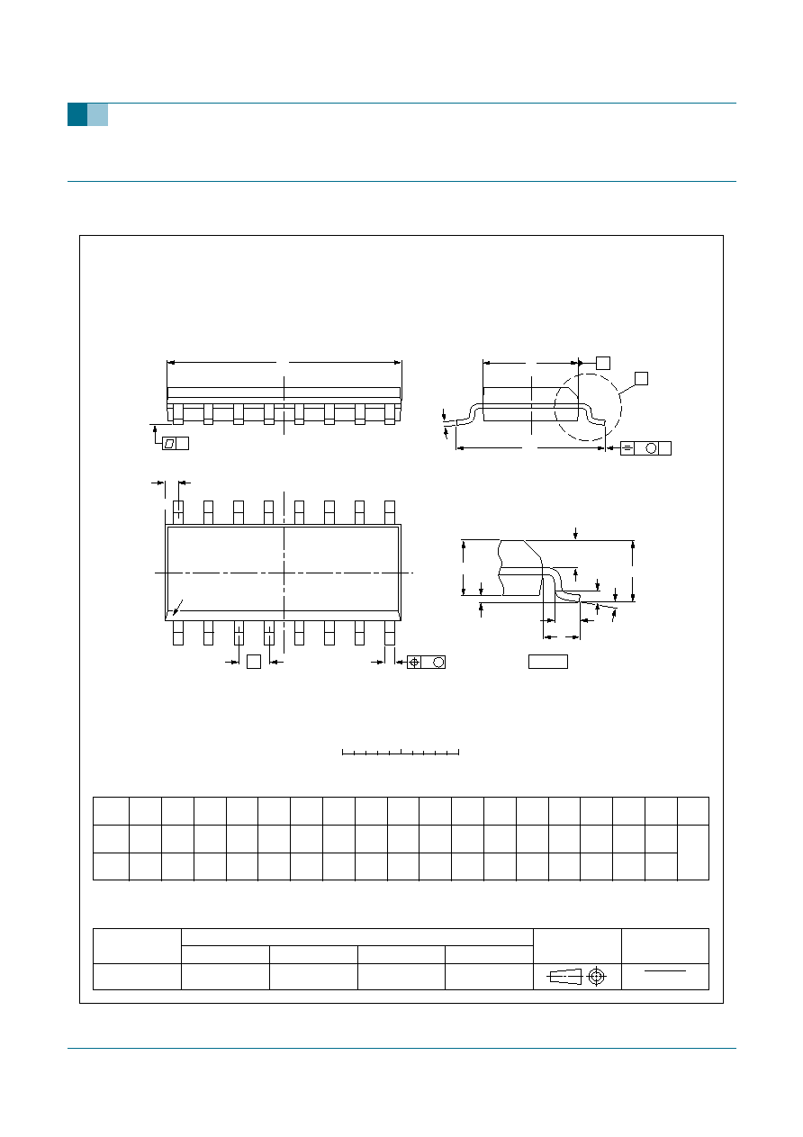
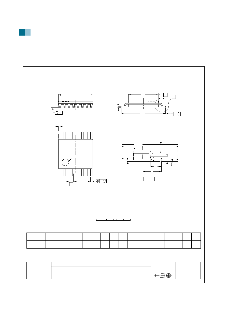
13. Package outline
Fig 18. Package outline SOT109-1 (SO16)
X
w
M
A
A
1
A
2
b
p
D
H
E
L
p
Q
detail X
E
Z
e
c
L
v
M
A
(A )
3
A
8
9
1
16
y
pin 1 index
UNIT
A
max.
A
1
A
2
A
3
b
p
c
D
(1)
E
(1)
(1)
e
H
E
L
L
p
Q
Z
y
w
v
REFERENCES
OUTLINE
VERSION
EUROPEAN
PROJECTION
ISSUE DATE
IEC
JEDEC
JEITA
mm
inches
1.75
0.25
0.10
1.45
1.25
0.25
0.49
0.36
0.25
0.19
10.0
9.8
4.0
3.8
1.27
6.2
5.8
0.7
0.6
0.7
0.3
8
0
o
o
0.25
0.1
DIMENSIONS (inch dimensions are derived from the original mm dimensions)
Note
1. Plastic or metal protrusions of 0.15 mm (0.006 inch) maximum per side are not included.
1.0
0.4
SOT109-1
99-12-27
03-02-19
076E07
MS-012
0.069
0.010
0.004
0.057
0.049
0.01
0.019
0.014
0.0100
0.0075
0.39
0.38
0.16
0.15
0.05
1.05
0.041
0.244
0.228
0.028
0.020
0.028
0.012
0.01
0.25
0.01
0.004
0.039
0.016
0
2.5
5 mm
scale
SO16: plastic small outline package; 16 leads; body width 3.9 mm
SOT109-1
9397 750 14318
� Koninklijke Philips Electronics N.V. 2005. All rights reserved.
Product data sheet
Rev. 03 -- 6 April 2005
18 of 25
Philips Semiconductors
PCA9546A
4-channel I
2
C switch with reset
Fig 19. Package outline SOT403-1 (TSSOP16)
UNIT
A
1
A
2
A
3
b
p
c
D
(1)
E
(2)
(1)
e
H
E
L
L
p
Q
Z
y
w
v
REFERENCES
OUTLINE
VERSION
EUROPEAN
PROJECTION
ISSUE DATE
IEC
JEDEC
JEITA
mm
0.15
0.05
0.95
0.80
0.30
0.19
0.2
0.1
5.1
4.9
4.5
4.3
0.65
6.6
6.2
0.4
0.3
0.40
0.06
8
0
o
o
0.13
0.1
0.2
1
DIMENSIONS (mm are the original dimensions)
Notes
1. Plastic or metal protrusions of 0.15 mm maximum per side are not included.
2. Plastic interlead protrusions of 0.25 mm maximum per side are not included.
0.75
0.50
SOT403-1
MO-153
99-12-27
03-02-18
w
M
b
p
D
Z
e
0.25
1
8
16
9
A
A
1
A
2
L
p
Q
detail X
L
(A )
3
H
E
E
c
v
M
A
X
A
y
0
2.5
5 mm
scale
TSSOP16: plastic thin shrink small outline package; 16 leads; body width 4.4 mm
SOT403-1
A
max.
1.1
pin 1 index
9397 750 14318
� Koninklijke Philips Electronics N.V. 2005. All rights reserved.
Product data sheet
Rev. 03 -- 6 April 2005
19 of 25
Philips Semiconductors
PCA9546A
4-channel I
2
C switch with reset
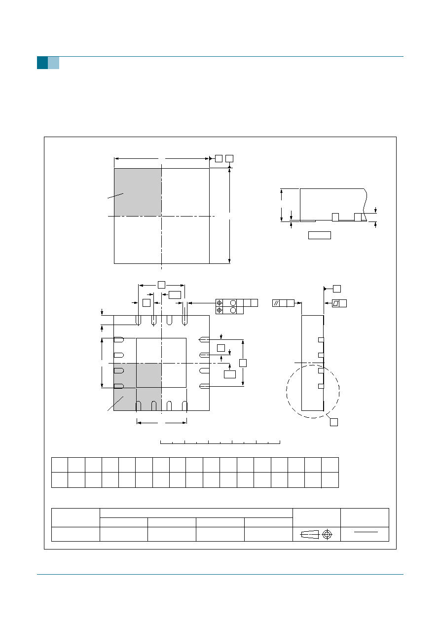
Fig 20. Package outline SOT629-1 (HVQFN16)
terminal 1
index area
0.65
1
A1
Eh
b
UNIT
y
e
0.2
c
REFERENCES
OUTLINE
VERSION
EUROPEAN
PROJECTION
ISSUE DATE
IEC
JEDEC
JEITA
mm
4.1
3.9
Dh
2.25
1.95
y1
4.1
3.9
2.25
1.95
e1
1.95
e2
1.95
0.38
0.23
0.05
0.00
0.05
0.1
DIMENSIONS (mm are the original dimensions)
SOT629-1
MO-220
- - -
- - -
0.75
0.50
L
0.1
v
0.05
w
0
2.5
5 mm
scale
SOT629-1
HVQFN16: plastic thermal enhanced very thin quad flat package; no leads;
16 terminals; body 4 x 4 x 0.85 mm
A
(1)
max.
A
A1
c
detail X
y
y1 C
e
L
Eh
Dh
e
e1
b
5
8
16
13
12
9
4
1
X
D
E
C
B
A
e2
01-08-08
02-10-22
terminal 1
index area
1/2
e
1/2
e
A
C
C
B
v
M
w
M
E
(1)
Note
1. Plastic or metal protrusions of 0.075 mm maximum per side are not included.
D
(1)

9397 750 14318
� Koninklijke Philips Electronics N.V. 2005. All rights reserved.
Product data sheet
Rev. 03 -- 6 April 2005
20 of 25
Philips Semiconductors
PCA9546A
4-channel I
2
C switch with reset
14. Soldering
14.1 Introduction to soldering surface mount packages
This text gives a very brief insight to a complex technology. A more in-depth account of
soldering ICs can be found in our
Data Handbook IC26; Integrated Circuit Packages
(document order number 9398 652 90011).
There is no soldering method that is ideal for all surface mount IC packages. Wave
soldering can still be used for certain surface mount ICs, but it is not suitable for fine pitch
SMDs. In these situations reflow soldering is recommended.
14.2 Reflow soldering
Reflow soldering requires solder paste (a suspension of fine solder particles, flux and
binding agent) to be applied to the printed-circuit board by screen printing, stencilling or
pressure-syringe dispensing before package placement. Driven by legislation and
environmental forces the worldwide use of lead-free solder pastes is increasing.
Several methods exist for reflowing; for example, convection or convection/infrared
heating in a conveyor type oven. Throughput times (preheating, soldering and cooling)
vary between 100 seconds and 200 seconds depending on heating method.
Typical reflow peak temperatures range from 215
�
C to 270
�
C depending on solder paste
material. The top-surface temperature of the packages should preferably be kept:
�
below 225
�
C (SnPb process) or below 245
�
C (Pb-free process)
� for all BGA, HTSSON..T and SSOP..T packages
� for packages with a thickness
2.5 mm
� for packages with a thickness < 2.5 mm and a volume
350 mm
3
so called
thick/large packages.
�
below 240
�
C (SnPb process) or below 260
�
C (Pb-free process) for packages with a
thickness < 2.5 mm and a volume < 350 mm
3
so called small/thin packages.
Moisture sensitivity precautions, as indicated on packing, must be respected at all times.
14.3 Wave soldering
Conventional single wave soldering is not recommended for surface mount devices
(SMDs) or printed-circuit boards with a high component density, as solder bridging and
non-wetting can present major problems.
To overcome these problems the double-wave soldering method was specifically
developed.
If wave soldering is used the following conditions must be observed for optimal results:
�
Use a double-wave soldering method comprising a turbulent wave with high upward
pressure followed by a smooth laminar wave.
�
For packages with leads on two sides and a pitch (e):
� larger than or equal to 1.27 mm, the footprint longitudinal axis is preferred to be
parallel to the transport direction of the printed-circuit board;
9397 750 14318
� Koninklijke Philips Electronics N.V. 2005. All rights reserved.
Product data sheet
Rev. 03 -- 6 April 2005
21 of 25
Philips Semiconductors
PCA9546A
4-channel I
2
C switch with reset
� smaller than 1.27 mm, the footprint longitudinal axis must be parallel to the
transport direction of the printed-circuit board.
The footprint must incorporate solder thieves at the downstream end.
�
For packages with leads on four sides, the footprint must be placed at a 45
�
angle to
the transport direction of the printed-circuit board. The footprint must incorporate
solder thieves downstream and at the side corners.
During placement and before soldering, the package must be fixed with a droplet of
adhesive. The adhesive can be applied by screen printing, pin transfer or syringe
dispensing. The package can be soldered after the adhesive is cured.
Typical dwell time of the leads in the wave ranges from 3 seconds to 4 seconds at 250
�
C
or 265
�
C, depending on solder material applied, SnPb or Pb-free respectively.
A mildly-activated flux will eliminate the need for removal of corrosive residues in most
applications.
14.4 Manual soldering
Fix the component by first soldering two diagonally-opposite end leads. Use a low voltage
(24 V or less) soldering iron applied to the flat part of the lead. Contact time must be
limited to 10 seconds at up to 300
�
C.
When using a dedicated tool, all other leads can be soldered in one operation within
2 seconds to 5 seconds between 270
�
C and 320
�
C.
14.5 Package related soldering information
[1]
For more detailed information on the BGA packages refer to the
(LF)BGA Application Note (AN01026);
order a copy from your Philips Semiconductors sales office.
[2]
All surface mount (SMD) packages are moisture sensitive. Depending upon the moisture content, the
maximum temperature (with respect to time) and body size of the package, there is a risk that internal or
external package cracks may occur due to vaporization of the moisture in them (the so called popcorn
effect). For details, refer to the Drypack information in the
Data Handbook IC26; Integrated Circuit
Packages; Section: Packing Methods.
[3]
These transparent plastic packages are extremely sensitive to reflow soldering conditions and must on no
account be processed through more than one soldering cycle or subjected to infrared reflow soldering with
peak temperature exceeding 217
�
C
�
10
�
C measured in the atmosphere of the reflow oven. The package
body peak temperature must be kept as low as possible.
Table 9:
Suitability of surface mount IC packages for wave and reflow soldering methods
Package
[1]
Soldering method
Wave
Reflow
[2]
BGA, HTSSON..T
[3]
, LBGA, LFBGA, SQFP,
SSOP..T
[3]
, TFBGA, VFBGA, XSON
not suitable
suitable
DHVQFN, HBCC, HBGA, HLQFP, HSO, HSOP,
HSQFP, HSSON, HTQFP, HTSSOP, HVQFN,
HVSON, SMS
not suitable
[4]
suitable
PLCC
[5]
, SO, SOJ
suitable
suitable
LQFP, QFP, TQFP
not recommended
[5] [6]
suitable
SSOP, TSSOP, VSO, VSSOP
not recommended
[7]
suitable
CWQCCN..L
[8]
, PMFP
[9]
, WQCCN..L
[8]
not suitable
not suitable

9397 750 14318
� Koninklijke Philips Electronics N.V. 2005. All rights reserved.
Product data sheet
Rev. 03 -- 6 April 2005
22 of 25
Philips Semiconductors
PCA9546A
4-channel I
2
C switch with reset
[4]
These packages are not suitable for wave soldering. On versions with the heatsink on the bottom side, the
solder cannot penetrate between the printed-circuit board and the heatsink. On versions with the heatsink
on the top side, the solder might be deposited on the heatsink surface.
[5]
If wave soldering is considered, then the package must be placed at a 45
�
angle to the solder wave
direction. The package footprint must incorporate solder thieves downstream and at the side corners.
[6]
Wave soldering is suitable for LQFP, QFP and TQFP packages with a pitch (e) larger than 0.8 mm; it is
definitely not suitable for packages with a pitch (e) equal to or smaller than 0.65 mm.
[7]
Wave soldering is suitable for SSOP, TSSOP, VSO and VSSOP packages with a pitch (e) equal to or larger
than 0.65 mm; it is definitely not suitable for packages with a pitch (e) equal to or smaller than 0.5 mm.
[8]
Image sensor packages in principle should not be soldered. They are mounted in sockets or delivered
pre-mounted on flex foil. However, the image sensor package can be mounted by the client on a flex foil by
using a hot bar soldering process. The appropriate soldering profile can be provided on request.
[9]
Hot bar soldering or manual soldering is suitable for PMFP packages.
15. Abbreviations
16. Revision history
Table 10:
Abbreviations
Acronym
Description
CDM
Charged Device Model
ESD
Electro Static Discharge
HBM
Human Body Model
IC
Integrated Circuit
LSB
Least Significant Bit
MM
Machine Model
MSB
Most Significant Bit
PCB
Printed-Circuit Board
Table 11:
Revision history
Document ID
Release date
Data sheet status
Change notice
Doc. number
Supersedes
PCA9546A_3
20050406
Product data sheet
-
9397 750 14318
PCA9546A_2
Modifications:
�
The format of this data sheet has been redesigned to comply with the new presentation and
information standard of Philips Semiconductors.
�
Section 2 "Features" on page 1
:
� 7th bullet: changed `RDS
ON
' to `R
on
'
� 16th bullet: changed `JESDEC' to `JEDEC'
�
Figure 4 "Pin configuration for HVQFN16 (transparent top view)" on page 4
:
� added pin 1 indicator notch and center pad
� changed pin 1 from `A2' to `RESET'
�
Section 6.2 "Pin description" on page 5
: added
Table note 1
and its reference at HVQFN pin 6.
�
Section 7.2.1 "Control register definition" on page 6
, third sentence: changed `The 2 LSBs of the
control byte ...' to `The 4 LSBs of the control byte ...'
�
Section 7.5 "Voltage translation" on page 7
:
�
Figure 7
modified and title changed from `V
pass
voltage versus V
DD
' to `Pass gate voltage versus
supply voltage'
� 2nd paragraph: changed symbol `V
pass
' and `V
pass(max)
' to `V
o(sw)
' and `V
o(sw)(max)
', respectively.

Philips Semiconductors
PCA9546A
4-channel I
2
C switch with reset
9397 750 14318
� Koninklijke Philips Electronics N.V. 2005. All rights reserved.
Product data sheet
Rev. 03 -- 6 April 2005
23 of 25
Modifications
(continued):
�
Added
Section 8.5 "Bus transactions" on page 10
; moved
Figure 12 "Write control register"
and
Figure 13 "Read control register"
to this section.
�
Table 5 "Limiting values" on page 12
:
� In the description line below table title, changed `referenced to GND' to `referenced to V
SS
'
� Removed (old) table note [1], as this statement is now covered in
Section 19 "Disclaimers"
�
Table 6 "DC characteristics" on page 13
:
� added (new)
Table note 1
� changed symbol `R
ON
' to `R
on
' and its parameter from `switch resistance' to `on-state resistance'
� changed symbol `V
pass
' to `V
o(sw)
'
� under Conditions column: changed `V
swin
' to `V
i(sw)
'; changed `I
swout
' to I
o(sw)
'
�
Table 7 "DC characteristics" on page 14
:
� added (new)
Table note 1
� sub-section `Select inputs A0 to A2, RESET': changed I
LI(max)
from `+50
�
A' to `+1
�
A'.
� sub-section `Pass gate': changed I
L(min)
from `
-
10
�
A' to `
-
1
�
A';
changed I
L(max)
from `+100
�
A' to `+1
�
A'
� changed symbol `R
ON
' to `R
on
' and its parameter from `switch resistance' to `on-state resistance'
� changed symbol `V
pass
' to `V
o(sw)
'
� under Conditions column: changed `V
swin
' to `V
i(sw)
'; changed `I
swout
' to I
o(sw)
'
�
Table 8 "Dynamic characteristics" on page 15
:
� symbol `t
R
' changed to `t
r
'; symbol `t
F
' changed to `t
f
'
� changed symbols `t
VD;DATL
' and `t
VD;DATH
' to `t
VD;DAT
' and added Conditions indicating
HIGH-to-LOW and LOW-to-HIGH transitions
� changed symbol `t
WL(rst)
' to `t
w(rst)L
'
� changed parameter for symbol t
REC;STA
from `recovery to START' to `recovery time to START
condition'
� in
Table note 1
: changed `R
ON
' to `R
on
'
�
Added
Figure 16
and
Figure 17
�
Added
Section 15 "Abbreviations"
PCA9546A_2
20040929
Objective data sheet
-
9397 750 13991
PCA9546A_1
PCA9546A_1
20040728
Objective data sheet
-
9397 750 13308
-
Table 11:
Revision history
...continued
Document ID
Release date
Data sheet status
Change notice
Doc. number
Supersedes

Philips Semiconductors
PCA9546A
4-channel I
2
C switch with reset
9397 750 14318
� Koninklijke Philips Electronics N.V. 2005. All rights reserved.
Product data sheet
Rev. 03 -- 6 April 2005
24 of 25
17. Data sheet status
[1]
Please consult the most recently issued data sheet before initiating or completing a design.
[2]
The product status of the device(s) described in this data sheet may have changed since this data sheet was published. The latest information is available on the Internet at
URL http://www.semiconductors.philips.com.
[3]
For data sheets describing multiple type numbers, the highest-level product status determines the data sheet status.
18. Definitions
Short-form specification -- The data in a short-form specification is
extracted from a full data sheet with the same type number and title. For
detailed information see the relevant data sheet or data handbook.
Limiting values definition -- Limiting values given are in accordance with
the Absolute Maximum Rating System (IEC 60134). Stress above one or
more of the limiting values may cause permanent damage to the device.
These are stress ratings only and operation of the device at these or at any
other conditions above those given in the Characteristics sections of the
specification is not implied. Exposure to limiting values for extended periods
may affect device reliability.
Application information -- Applications that are described herein for any
of these products are for illustrative purposes only. Philips Semiconductors
make no representation or warranty that such applications will be suitable for
the specified use without further testing or modification.
19. Disclaimers
Life support -- These products are not designed for use in life support
appliances, devices, or systems where malfunction of these products can
reasonably be expected to result in personal injury. Philips Semiconductors
customers using or selling these products for use in such applications do so
at their own risk and agree to fully indemnify Philips Semiconductors for any
damages resulting from such application.
Right to make changes -- Philips Semiconductors reserves the right to
make changes in the products - including circuits, standard cells, and/or
software - described or contained herein in order to improve design and/or
performance. When the product is in full production (status `Production'),
relevant changes will be communicated via a Customer Product/Process
Change Notification (CPCN). Philips Semiconductors assumes no
responsibility or liability for the use of any of these products, conveys no
license or title under any patent, copyright, or mask work right to these
products, and makes no representations or warranties that these products are
free from patent, copyright, or mask work right infringement, unless otherwise
specified.
20. Contact information
For additional information, please visit: http://www.semiconductors.philips.com
For sales office addresses, send an email to: sales.addresses@www.semiconductors.philips.com
Level
Data sheet status
[1]
Product status
[2] [3]
Definition
I
Objective data
Development
This data sheet contains data from the objective specification for product development. Philips
Semiconductors reserves the right to change the specification in any manner without notice.
II
Preliminary data
Qualification
This data sheet contains data from the preliminary specification. Supplementary data will be published
at a later date. Philips Semiconductors reserves the right to change the specification without notice, in
order to improve the design and supply the best possible product.
III
Product data
Production
This data sheet contains data from the product specification. Philips Semiconductors reserves the
right to make changes at any time in order to improve the design, manufacturing and supply. Relevant
changes will be communicated via a Customer Product/Process Change Notification (CPCN).

� Koninklijke Philips Electronics N.V. 2005
All rights are reserved. Reproduction in whole or in part is prohibited without the prior
written consent of the copyright owner. The information presented in this document does
not form part of any quotation or contract, is believed to be accurate and reliable and may
be changed without notice. No liability will be accepted by the publisher for any
consequence of its use. Publication thereof does not convey nor imply any license under
patent- or other industrial or intellectual property rights.
Date of release: 6 April 2005
Document number: 9397 750 14318
Published in The Netherlands
Philips Semiconductors
PCA9546A
4-channel I
2
C switch with reset
21. Contents
1
General description . . . . . . . . . . . . . . . . . . . . . . 1
2
Features . . . . . . . . . . . . . . . . . . . . . . . . . . . . . . . 1
3
Ordering information . . . . . . . . . . . . . . . . . . . . . 2
4
Marking . . . . . . . . . . . . . . . . . . . . . . . . . . . . . . . . 2
5
Block diagram . . . . . . . . . . . . . . . . . . . . . . . . . . 3
6
Pinning information . . . . . . . . . . . . . . . . . . . . . . 4
6.1
Pinning . . . . . . . . . . . . . . . . . . . . . . . . . . . . . . . 4
6.2
Pin description . . . . . . . . . . . . . . . . . . . . . . . . . 5
7
Functional description . . . . . . . . . . . . . . . . . . . 5
7.1
Device address . . . . . . . . . . . . . . . . . . . . . . . . . 5
7.2
Control register . . . . . . . . . . . . . . . . . . . . . . . . . 6
7.2.1
Control register definition . . . . . . . . . . . . . . . . . 6
7.3
RESET input . . . . . . . . . . . . . . . . . . . . . . . . . . . 7
7.4
Power-on reset . . . . . . . . . . . . . . . . . . . . . . . . . 7
7.5
Voltage translation . . . . . . . . . . . . . . . . . . . . . . 7
8
Characteristics of the I
2
C-bus. . . . . . . . . . . . . . 8
8.1
Bit transfer . . . . . . . . . . . . . . . . . . . . . . . . . . . . 8
8.2
START and STOP conditions . . . . . . . . . . . . . . 8
8.3
System configuration . . . . . . . . . . . . . . . . . . . . 8
8.4
Acknowledge . . . . . . . . . . . . . . . . . . . . . . . . . . 9
8.5
Bus transactions . . . . . . . . . . . . . . . . . . . . . . . 10
9
Application design-in information . . . . . . . . . 11
10
Limiting values. . . . . . . . . . . . . . . . . . . . . . . . . 12
11
Static characteristics. . . . . . . . . . . . . . . . . . . . 13
12
Dynamic characteristics . . . . . . . . . . . . . . . . . 15
13
Package outline . . . . . . . . . . . . . . . . . . . . . . . . 17
14
Soldering . . . . . . . . . . . . . . . . . . . . . . . . . . . . . 20
14.1
Introduction to soldering surface mount
packages . . . . . . . . . . . . . . . . . . . . . . . . . . . . 20
14.2
Reflow soldering . . . . . . . . . . . . . . . . . . . . . . . 20
14.3
Wave soldering . . . . . . . . . . . . . . . . . . . . . . . . 20
14.4
Manual soldering . . . . . . . . . . . . . . . . . . . . . . 21
14.5
Package related soldering information . . . . . . 21
15
Abbreviations . . . . . . . . . . . . . . . . . . . . . . . . . . 22
16
Revision history . . . . . . . . . . . . . . . . . . . . . . . . 22
17
Data sheet status . . . . . . . . . . . . . . . . . . . . . . . 24
18
Definitions . . . . . . . . . . . . . . . . . . . . . . . . . . . . 24
19
Disclaimers . . . . . . . . . . . . . . . . . . . . . . . . . . . . 24
20
Contact information . . . . . . . . . . . . . . . . . . . . 24