PCF2113x
LCD controllers/drivers
DATA SHEET
Product specification
Supersedes data of 1997 Apr 04
File under Integrated Circuits, IC12
2001 Dec 19
INTEGRATED CIRCUITS

2001 Dec 19
2
Philips Semiconductors
Product specification
LCD controllers/drivers
PCF2113x
CONTENTS
1
FEATURES
1.1
Note
2
APPLICATIONS
3
GENERAL DESCRIPTION
4
ORDERING INFORMATION
5
BLOCK DIAGRAM
6
PINNING
7
FUNCTIONAL DESCRIPTION
7.1
LCD supply voltage generator
7.2
LCD bias voltage generator
7.3
Oscillator
7.4
External clock
7.5
Power-on reset
7.6
Power-down mode
7.7
Registers
7.8
Busy flag
7.9
Address Counter (AC)
7.10
Display Data RAM (DDRAM)
7.11
Character Generator ROM (CGROM)
7.12
Character Generator RAM (CGRAM)
7.13
Cursor control circuit
7.14
Timing generator
7.15
LCD row and column drivers
7.16
Reset function
8
INSTRUCTIONS
8.1
Clear display
8.2
Return home
8.3
Entry mode set
8.4
Display control (and partial Power-down mode)
8.5
Cursor or display shift
8.6
Function set
8.7
Set CGRAM address
8.8
Set DDRAM address
8.9
Read busy flag and read address
8.10
Write data to CGRAM or DDRAM
8.11
Read data from CGRAM or DDRAM
9
EXTENDED FUNCTION SET
INSTRUCTIONS AND FEATURES
9.1
New instructions
9.2
Icon control
9.3
Bit IM
9.4
Bit IB
9.5
Direct mode
9.6
Voltage multiplier control
9.7
Screen configuration
9.8
Display configuration
9.9
Temperature control
9.10
Set V
LCD
9.11
Reducing current consumption
10
INTERFACES TO MICROCONTROLLER
10.1
Parallel interface
10.2
I
2
C-bus interface
11
LIMITING VALUES
12
HANDLING INSTRUCTIONS
13
DC CHARACTERISTICS
14
AC CHARACTERISTICS
15
DEVICE PROTECTION CIRCUITS
16
APPLICATION INFORMATION
16.1
General application information
16.2
4-bit operation, 1-line display using internal
reset
16.3
8-bit operation, 1-line display using internal
reset
16.4
8-bit operation, 2-line display
16.5
I
2
C-bus operation, 1-line display
17
BONDING PAD INFORMATION
18
TRAY INFORMATION
19
PACKAGE OUTLINE
20
SOLDERING
20.1
Introduction to soldering surface mount
packages
20.2
Reflow soldering
20.3
Wave soldering
20.4
Manual soldering
20.5
Suitability of surface mount IC packages for
wave and reflow soldering methods
21
DATA SHEET STATUS
22
DEFINITIONS
23
DISCLAIMERS
24
BARE DIE DISCLAIMER
25
PURCHASE OF PHILIPS I
2
C COMPONENTS

2001 Dec 19
3
Philips Semiconductors
Product specification
LCD controllers/drivers
PCF2113x
1
FEATURES
∑
Single-chip LCD controller/driver
∑
2-line display of up to 12 characters + 120 icons, or
1-line display of up to 24 characters + 120 icons
∑
5
◊
7 character format plus cursor; 5
◊
8 for kana
(Japanese) and user defined symbols
∑
Icon mode: reduced current consumption while
displaying
∑
Icon blink function
∑
On-chip:
≠ Configurable 4, 3 or 2 voltage multiplier generating
LCD supply voltage, independent of V
DD
,
programmable by instruction (external supply also
possible)
≠ Temperature compensation of on-chip generated
V
LCD
:
-
0.16 to
-
0.24 %/K (programmable by
instruction)
≠ Generation of intermediate LCD bias voltages
≠ Oscillator requires no external components
(external clock also possible).
∑
Display data RAM: 80 characters
∑
Character generator ROM: 240, 5
◊
8 characters
∑
Character generator RAM: 16, 5
◊
8 characters;
3 characters used to drive 120 icons, 6 characters used
if icon blink feature is used in application
∑
4 or 8-bit parallel bus and 2-wire I
2
C-bus interface
∑
CMOS compatible
∑
18 row and 60 column outputs
∑
Multiplex rates 1 : 18 (for normal operation), 1 : 9 (for
single line operation) and 1 : 2 (for icon only mode)
∑
Uses common 11 code instruction set (extended)
∑
Logic supply voltage range V
DD1
-
V
SS1
= 1.8 to 5.5 V
(chip may be driven with two battery cells)
∑
V
LCD
generator supply voltage range
V
DD2
-
V
SS2
= 2.2 to 4.0 V
∑
Display supply voltage range V
LCD
-
V
SS2
= 2.2 to 6.5 V
∑
Direct mode to save current consumption for icon mode
and Mux 1 : 9 (depending on V
DD2
value and LCD liquid
properties)
∑
Very low current consumption (20 to 200
µ
A):
≠ Icon mode: <25
µ
A
≠ Power-down mode: <2
µ
A.
1.1
Note
Icon mode is used to save current. When only icons are
displayed, a much lower operating voltage V
LCD
can be
used and the switching frequency of the LCD outputs is
reduced. In most applications it is possible to use V
DD
as
V
LCD
.
2
APPLICATIONS
∑
Telecom equipment
∑
Portable instruments
∑
Point-of-sale terminals.
3
GENERAL DESCRIPTION
The PCF2113x is a low power CMOS LCD controller and
driver, designed to drive a dot matrix LCD display of 2-line
by 12 or 1-line by 24 characters with 5
◊
8 dot format.
All necessary functions for the display are provided in a
single chip, including on-chip generation of LCD bias
voltages, resulting in a minimum of external components
and lower system current consumption. The PCF2113x
interfaces to most microcontrollers via a 4 or 8-bit bus or
via the 2-wire I
2
C-bus. The chip contains a character
generator and displays alphanumeric and kana
(Japanese) characters. The letter `x' in PCF2113x
characterizes the built-in character set. Various character
sets can be manufactured on request.
2001 Dec 19
4
Philips Semiconductors
Product specification
LCD controllers/drivers
PCF2113x
4
ORDERING INFORMATION
TYPE NUMBER
PACKAGE
NAME
DESCRIPTION
VERSION
PCF2113AU/10/F4
-
chip on flexible film carrier
-
PCF2113DU/10/F4
-
chip on flexible film carrier
-
PCF2113DU/F4
-
chip in tray
-
PCF2113DH/F4
LQFP100
plastic low profile quad flat package; 100 leads;
body 14
◊
14
◊
1.4 mm
SOT407-1
PCF2113DU/2/F4
-
chip with bumps in tray
-
PCF2113EU/2/F4
-
chip with bumps in tray
-
PCF2113WU/2/F4
-
chip with bumps in tray
-
2001 Dec 19
5
Philips Semiconductors
Product specification
LCD controllers/drivers
PCF2113x
5
BLOCK DIAGRAM
handbook, full pagewidth
MGE990
CURSOR AND DATA CONTROL
SHIFT REGISTER 5
◊
12 BIT
DATA LATCHES
COLUMN DRIVERS
60
5
60
CHARACTER
GENERATOR
RAM (128
◊
5)
(CGRAM)
16 CHARACTERS
CHARACTER
GENERATOR
ROM
(CGROM)
240 CHARACTERS
DISPLAY DATA RAM
(DDRAM)
80 CHARACTERS/BYTES
ADDRESS COUNTER
(AC)
INSTRUCTION
DECODER
INSTRUCTION
REGISTER(IR)
ROW DRIVERS
SHIFT REGISTER 18-BIT
BIAS
VOLTAGE
GENERATOR
VLCD
GENERATOR
VLCDSENSE
BUSY
FLAG
DATA
REGISTER
(DR)
I/O BUFFER
OSCILLATOR
TIMING
GENERATOR
DISPLAY
ADDRESS
COUNTER
POWER-ON
RESET
VDD1
VLCD2
VSS1
T1
VLCD1
VSS2
T2
T3
VDD2
VDD3
C1 to C60
R1 to R18
OSC
PD
PCF2113x
DB0 to DB3/SA0
DB4 to DB7
E
R/W
RS
SCL
SDA
18
18
60
5
7
7
7
8
7
7
8
8
8
Fig.1 Block diagram.

2001 Dec 19
6
Philips Semiconductors
Product specification
LCD controllers/drivers
PCF2113x
6
PINNING
SYMBOL
PIN
PCF2113DH
PAD
(1)
PCF2113XU
TYPE
DESCRIPTION
V
DD1
1
1
P
supply voltage 1 for all except V
LCD
generator
OSC
2
2
I
oscillator/external clock input; note 2
PD
3
3
I
power-down select input; for normal operation PD is LOW
T3
-
4
I
test pad; open circuit and not user accessible
T1
4
5
I
test pin; must be connected to V
SS1
T2
-
6
I
test pad; must be connected to V
SS1
V
SS1
5
7
P
ground 1 for all except V
LCD
generator
V
SS2
6
8
P
ground 2 for V
LCD
generator
V
LCD2
7
9
O
V
LCD
output if V
LCD
is generated internally; note 7
V
LCDSENSE
-
10
I
input (V
LCD
) for voltage multiplier regulation; notes 3 and 7
V
LCD1
8
11
I
input for generation of LCD bias levels; note 7
R9 to R16
9 to 16
12 to 19
O
LCD row driver outputs 9 to 16
R18
17
20
O
LCD row driver output 18
C60 to C53
18 to 25
21 to 28
O
LCD column driver outputs 60 to 53
dummy pad
-
29
-
dummy pad
-
30
-
C52 to C28
26 to 50
31 to 55
O
LCD column driver outputs 52 to 28
dummy pad
-
56
-
dummy pad
-
57
-
C27 to C3
51 to 75
58 to 82
O
LCD column driver outputs 27 to 3
dummy pad
-
83
-
dummy pad
-
84
-
C2
76
85
O
LCD column driver output 2
C1
77
86
O
LCD column driver output 1
R8 to R1
78 to 85
87 to 94
O
LCD row driver outputs 8 to 1
R17
86
95
O
LCD row driver output 17
SCL
87
96
I
I
2
C-bus serial clock input; note 4
SDA
88
97
I/O
I
2
C-bus serial data input/output; note 4
E
89
98
I
data bus clock input; note 4
RS
90
99
I
register select input
R/W
91
100
I
read/write input
DB7
92
101
I/O
8-bit bidirectional data bus bit 7; note 5
DB6
93
102
I/O
8-bit bidirectional data bus bit 6
DB5
94
103
I/O
8-bit bidirectional data bus bit 5
DB4
95
104
I/O
8-bit bidirectional data bus bit 4
DB3/SA0
96
105
I/O
8-bit bidirectional data bus bit 3 or I
2
C-bus address pin;
notes 4 and 5
DB2
97
106
I/O
8-bit bidirectional data bus bit 2
DB1
98
107
I/O
8-bit bidirectional data bus bit 1

2001 Dec 19
7
Philips Semiconductors
Product specification
LCD controllers/drivers
PCF2113x
Notes
1. Bonding pad location information is given in Chapter 17.
2. When the on-chip oscillator is used this pad must be connected to V
DD1
.
3. In the LQFP100 version this signal is connected internally and can not be accessed at any pin.
4. When the I
2
C-bus is used, the parallel interface pin E must be LOW. In the I
2
C-bus read mode DB7 to DB0 should
be connected to V
DD1
or left open-circuit.
When the parallel bus is used, the pins SCL and SDA must be connected to V
SS1
or V
DD1
; they must not be left
open-circuit.
When the 4-bit interface is used without reading out from the PCF2113x (R/W is set permanently to logic 0), the
unused ports DB0 to DB4 can either be set to V
SS1
or V
DD1
instead of leaving them open-circuit.
5. DB7 may be used as the busy flag, signalling that internal operations are not yet completed. In 4-bit operations the
four higher order lines DB7 to DB4 are used; DB3 to DB0 must be left open-circuit except for I
2
C-bus operations
(see note 4).
6. V
DD2
and V
DD3
should always be equal.
7. When V
LCD
is generated internally, pins V
LCD1
, V
LCD2
and V
LCDSENSE
must be connected together. When external
V
LCD
is supplied, pin V
LCD2
should be left open-circuit to avoid any stray current, pins V
LCD1
and V
LCDSENSE
must be
connected together.
DB0
99
108
I/O
8-bit bidirectional data bus bit 0
V
DD2
100
109
P
supply voltage 2 for V
LCD
generator; note 6
V
DD3
-
110
P
supply voltage 3 for V
LCD
generator; notes 3 and 6
SYMBOL
PIN
PCF2113DH
PAD
(1)
PCF2113XU
TYPE
DESCRIPTION
2001 Dec 19
8
Philips Semiconductors
Product specification
LCD controllers/drivers
PCF2113x
handbook, full pagewidth
75
74
73
72
71
70
69
68
67
66
65
64
63
62
61
60
59
58
57
56
55
54
53
52
51
80
79
78
77
76
R6
R7
R8
C1
C2
C3
C4
C5
C6
C7
C8
C9
C10
C11
C12
C13
C14
C15
C16
C17
C18
C19
C20
C21
C22
C23
C24
C25
C26
C27
VDD1
OSC
PD
T1
VSS1
VSS2
VLCD2
VLCD1
R9
R10
R11
R12
R13
R14
R15
R16
R18
C60
C59
C58
C57
C56
C55
C54
C53
C47
C46
C45
C44
C43
C42
C41
C40
C39
C38
C37
C36
C35
C34
C33
C32
C31
C30
C29
C28
V
DD2
DB0
DB1
DB2
DB3/SA0
DB4
DB5
DB6
DB7
R/W
RS
E
SDA
SCL
R17
R1
R2
R3
R4
R5
C52
C51
C50
C49
C48
30
29
28
27
26
25
24
23
22
21
20
19
18
17
16
15
14
13
12
11
10
9
8
7
6
5
4
3
2
1
100
99
98
97
96
95
94
93
92
91
90
89
88
87
86
85
84
83
82
81
31
32
33
34
35
36
37
38
39
40
41
42
43
44
45
46
47
48
49
50
PCF2113x
MGE989
Fig.2 Pin configuration (LQFP100).

2001 Dec 19
9
Philips Semiconductors
Product specification
LCD controllers/drivers
PCF2113x
7
FUNCTIONAL DESCRIPTION
7.1
LCD supply voltage generator
The LCD supply voltage may be generated on-chip. The
V
LCD
generator is controlled by two internal 6-bit registers:
V
A
and V
B
. The nominal LCD operating voltage at room
temperature is given by the relationship:
V
OP(nom)
= (integer value of register
◊
0.08) + 1.82
7.1.1
P
ROGRAMMING RANGES
Programmed value: 1 to 63. Voltage: 1.90 to 6.86 V.
T
ref
= 27
∞
C.
Values producing more than 6.5 V at operating
temperature are not allowed. Operation above this
voltage may damage the device. When programming the
operating voltage the V
LCD
tolerance and temperature
coefficient must be taken into account.
Values below 2.2 V are below the specified operating
range of the chip and are therefore not allowed.
Value 0 for V
A
and V
B
switches the generator off
(i.e. V
A
= 0 in character mode, V
B
= 0 in icon mode).
Usually register V
A
is programmed with the voltage for
character mode and register V
B
with the voltage for icon
mode.
When V
LCD
is generated on-chip the V
LCD
pins should be
decoupled to V
SS
with a suitable capacitor.
The generated V
LCD
is independent of V
DD
and is
temperature compensated. When the V
LCD
generator and
the direct mode are switched off, an external voltage may
be supplied at connected pins V
LCD1
and V
LCD2
. V
LCD1
and
V
LCD2
may be higher or lower than V
DD2
.
During direct mode (program DM register bit) the internal
V
LCD
generator is turned off and the V
LCD2
output voltage
is directly connected to V
DD2
. This reduces the current
consumption during icon mode and Mux 1 : 9 (depending
on V
DD2
value and LCD liquid properties).
The V
LCD
generator ensures that, as long as V
DD
is in the
valid range (2.2 to 4 V), the required peak voltage
V
OP
= 6.5 V can be generated at any time.
7.2
LCD bias voltage generator
The intermediate bias voltages for the LCD display are
also generated on-chip. This removes the need for an
external resistive bias chain and significantly reduces the
system current consumption. The optimum value of V
LCD
depends on the multiplex rate, the LCD threshold voltage
(V
th
) and the number of bias levels. Using a 5-level bias
scheme for 1 : 18 maximum rate allows V
LCD
< 5 V for
most LCD liquids. The intermediate bias levels for the
different multiplex rates are shown in Table 1. These bias
levels are automatically set to the given values when
switching to the corresponding multiplex rate.
Table 1
Bias levels as a function of multiplex rate; note 1
Note
1. The values in the table are given relative to V
LCD
-
V
SS
, e.g.
3
/
4
means
3
/
4
◊
(V
LCD
-
V
SS
).
MULTIPLEX
RATE
NUMBER
OF LEVELS
V
1
V
2
V
3
V
4
V
5
V
6
1 : 18
5
V
LCD
3
/
4
1
/
2
1
/
2
1
/
4
V
SS
1 : 9
5
V
LCD
3
/
4
1
/
2
1
/
2
1
/
4
V
SS
1 : 2
4
V
LCD
2
/
3
2
/
3
1
/
3
1
/
3
V
SS

2001 Dec 19
10
Philips Semiconductors
Product specification
LCD controllers/drivers
PCF2113x
7.3
Oscillator
The on-chip oscillator provides the clock signal for the
display system. No external components are required and
the OSC pin must be connected to V
DD1
.
7.4
External clock
If an external clock is to be used this input is at the OSC
pin. The resulting display frame frequency is given by:
Only in the Power-down mode is the clock allowed to be
stopped (OSC connected to V
SS
), otherwise the LCD is
frozen in a DC state.
7.5
Power-on reset
The on-chip Power-on reset block initializes the chip after
power-on or power failure. This is a synchronous reset and
requires 3 oscillator cycles to be executed.
7.6
Power-down mode
The chip can be put into Power-down mode by applying an
external active HIGH level to the PD pin. In Power-down
mode all static currents are switched off (no internal
oscillator, no bias level generation and all LCD outputs are
internally connected to V
SS
).
During power-down, information in the RAMs and the chip
state are preserved. Instruction execution during
power-down is possible when pin OSC is externally
clocked.
7.7
Registers
The PCF2113x has two 8-bit registers, an Instruction
Register (IR) and a Data Register (DR). The Register
Select (RS) signal determines which register will be
accessed. The instruction register stores instruction codes
such as `display clear', `cursor shift', and address
information for the Display Data RAM (DDRAM) and
Character Generator RAM (CGRAM).The instruction
register can be written to but not read from by the system
controller.
The data register temporarily stores data to be read from
the DDRAM and CGRAM. When reading, data from the
DDRAM or CGRAM corresponding to the address in the
instruction register is written to the data register prior to
being read by the `read data' instruction.
7.8
Busy flag
The busy flag indicates the internal status of the
PCF2113x. A logic 1 indicates that the chip is busy and
further instructions will not be accepted. The busy flag is
output to pin DB7 when bit RS = 0 and bit R/W = 1.
Instructions should only be written after checking that the
busy flag is at logic 0 or waiting for the required number of
cycles.
7.9
Address Counter (AC)
The address counter assigns addresses to the DDRAM
and CGRAM for reading and writing and is set by the
commands `set CGRAM address' and `set DDRAM
address'. After a read/write operation the address counter
is automatically incremented or decremented by 1.
The address counter contents are output to the bus
(DB6 to DB0) when bit RS = 0 and bit R/W = 1.
7.10
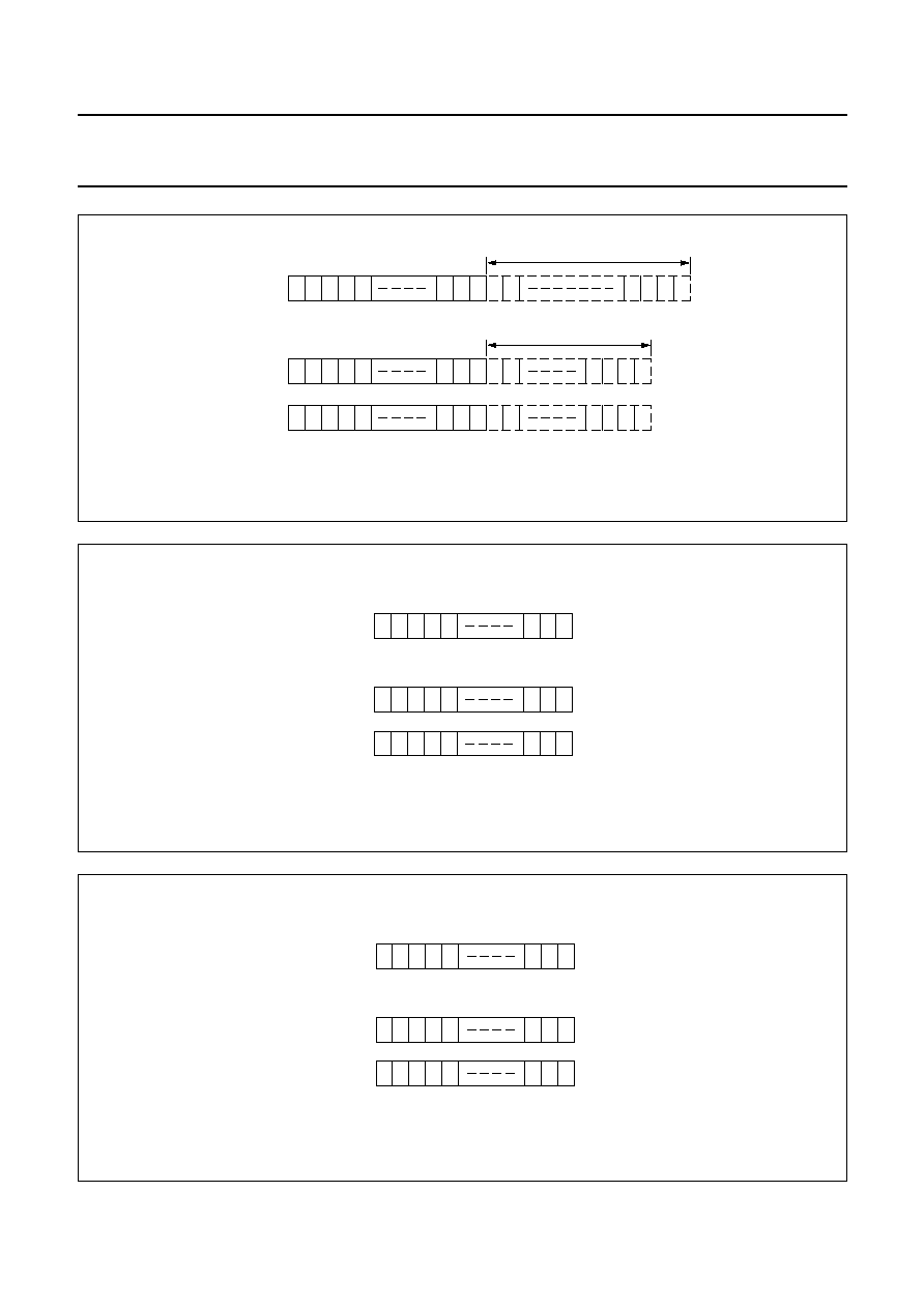
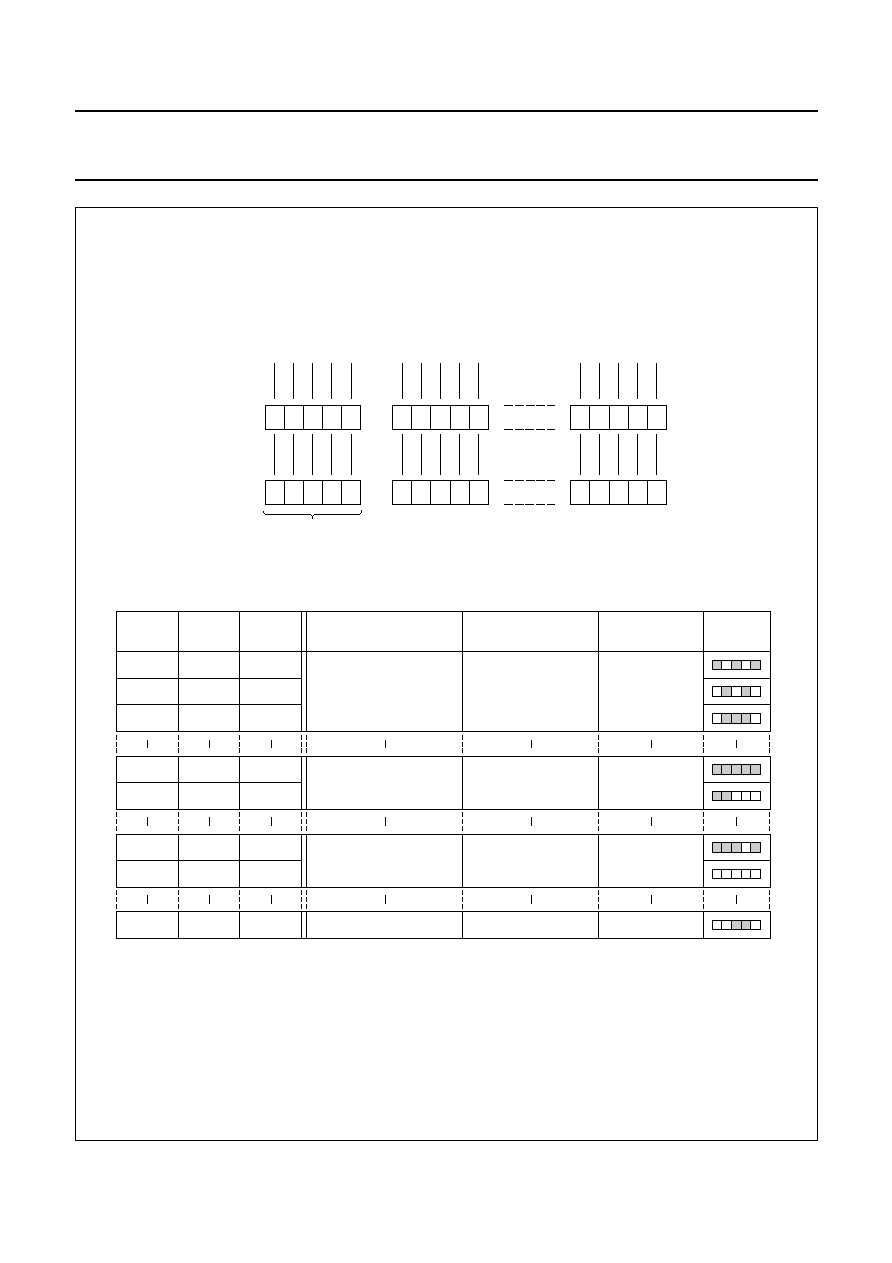
Display Data RAM (DDRAM)
The DDRAM stores up to 80 characters of display data
represented by 8-bit character codes. RAM locations
which are not used for storing display data can be used as
general purpose RAM. The basic RAM to display
addressing scheme is shown in Fig.3. With no display shift
the characters represented by the codes in the first
24 RAM locations starting at address 00H in line 1 are
displayed. Figures 4 and 5 show the display mapping for
right and left shift respectively.
When data is written to or read from the DDRAM,
wrap-around occurs from the end of one line to the start of
the next line. When the display is shifted each line wraps
around within itself, independently of the others. Thus all
lines are shifted and wrapped around together.
The address ranges and wrap-around operations for the
various modes are shown in Table 2.
f
frame
f
OSC
3 072
-------------
=
Table 2
Address space and wrap-around operation
MODE
1
◊
24
2
◊
12
1
◊
12
Address space
00 to 4F
00 to 27; 40 to 67
00 to 27
Read/write wrap-around (moves to next line)
4F to 00
27 to 40; 67 to 00
27 to 00
Display shift wrap-around (stays within line)
4F to 00
27 to 00; 67 to 40
27 to 00
2001 Dec 19
11
Philips Semiconductors
Product specification
LCD controllers/drivers
PCF2113x
handbook, full pagewidth
00 01 02 03 04
15 16 17 18 19
4C 4D 4E 4F
non-displayed DDRAM addresses
64 65 66 67
40 41 42 43 44
49 4A 4B 4C 4D
00 01 02 03 04
09 0A 0B 0C 0D
24 25 26 27
non-displayed DDRAM address
line 1
line 2
MGE991
DDRAM
address
2-line display
1
2
3
4
5
22 23 24
1
2
3
4
5
10 11 12
1
2
3
4
5
10 11 12
display
position
DDRAM
address
1-line display
Fig.3 DDRAM to display mapping; no shift.
handbook, halfpage
MGE992
27 00 01 02 03
67 40 41 42 43
08 09 0A
48 49 4A
DDRAM
address
line 1
line 2
2-line display
1
2
3
4
5
22 23 24
1
2
3
4
5
10 11 12
1
2
3
4
5
10 11 12
4F 00 01 02 03
14 15 16
display
position
DDRAM
address
1-line display
Fig.4 DDRAM to display mapping; right shift.
handbook, halfpage
01
04 05
41 42 43 44 45
0A 0B 0C
4A 4B 4C
DDRAM
address
line 1
line 2
2-line display
1
2
3
4
5
22 23 24
1
2
3
4
5
10 11 12
1
2
3
4
5
10 11 12
01
04 05
02 03
02 03
16 17 18
display
position
DDRAM
address
1-line display
MGE993
Fig.5 DDRAM to display mapping; left shift.
2001 Dec 19
12
Philips Semiconductors
Product specification
LCD controllers/drivers
PCF2113x
7.11
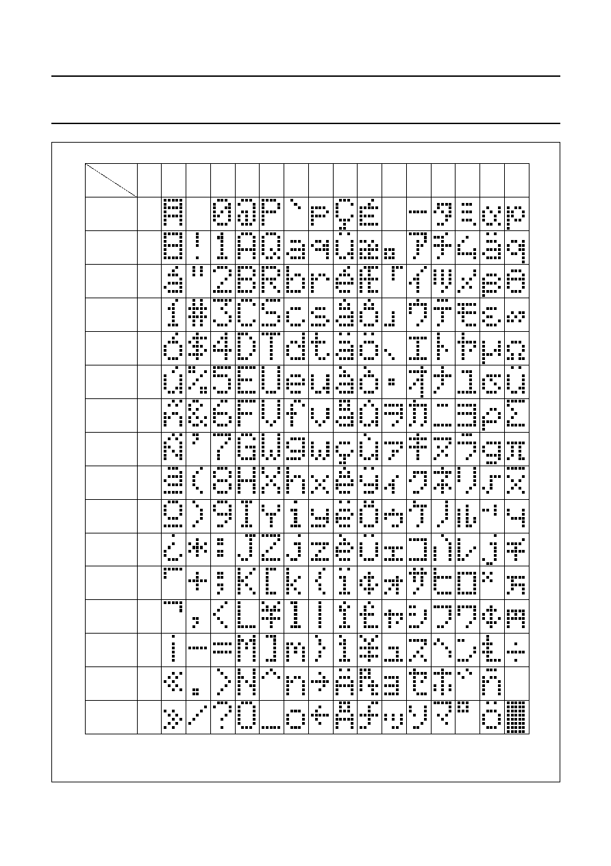
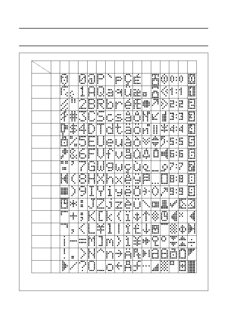
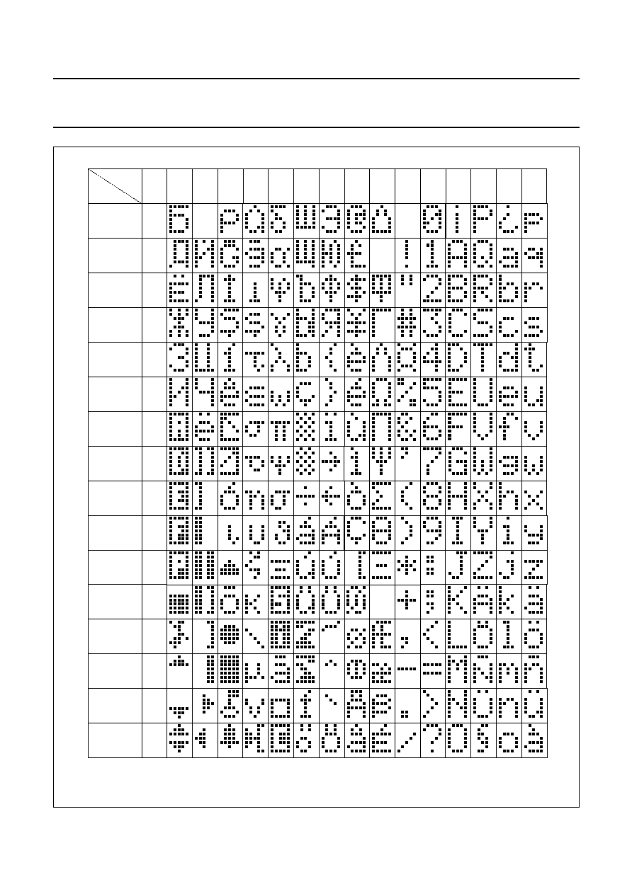
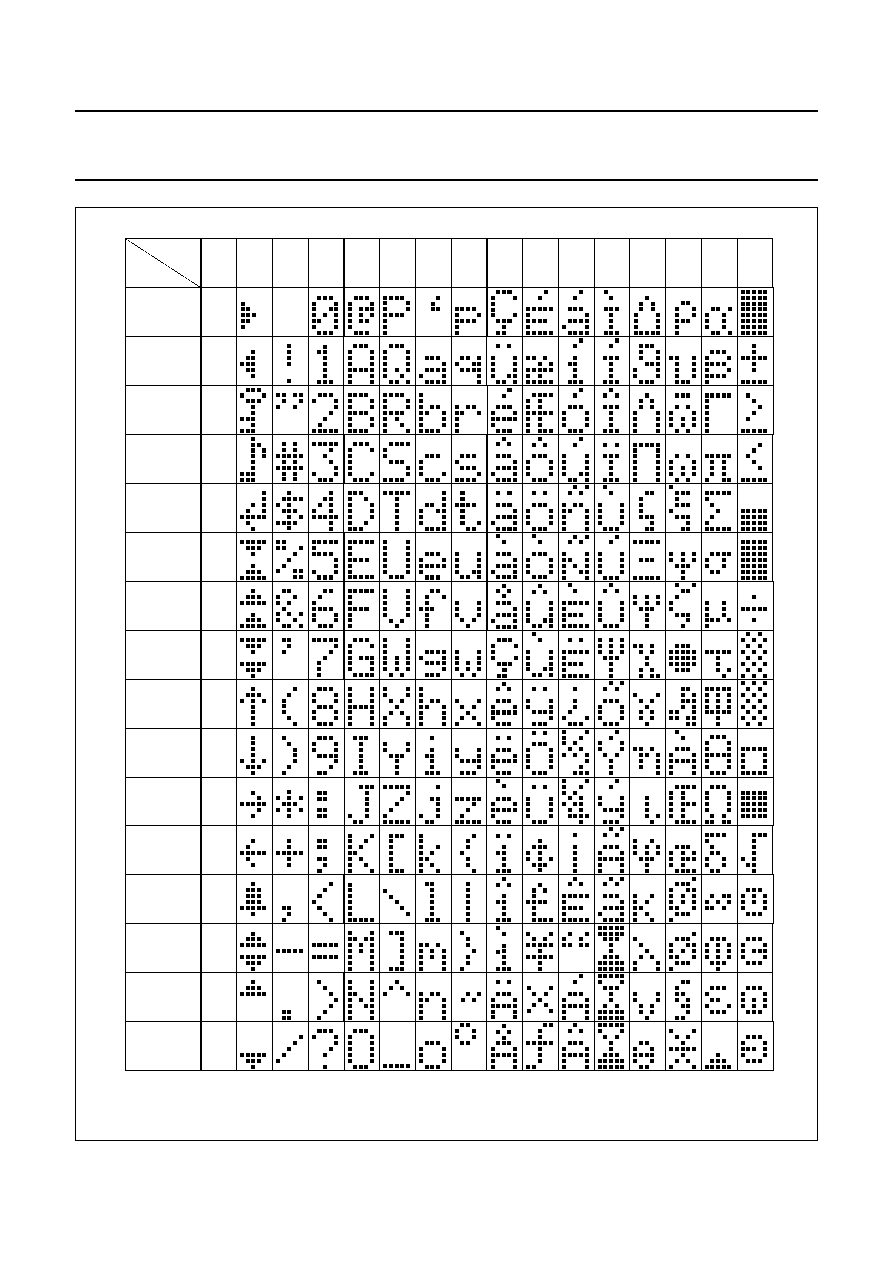
Character Generator ROM (CGROM)
The CGROM generates 240 character patterns in a
5
◊
8 dot format from 8-bit character codes.
Figures 7, 8, 9 and 10 show the character sets that are
currently implemented.
7.12
Character Generator RAM (CGRAM)
Up to 16 user defined characters may be stored in the
CGRAM. Some CGRAM characters (see Fig.16) are also
used to drive icons (6 if icons blink and both icon rows are
used in the application; 3 if no blink but both icon rows are
used in the application; 0 if no icons are driven by the icon
rows). The CGROM and CGRAM use a common address
space, of which the first column is reserved for the
CGRAM (see Fig.7). Figure 11 shows the addressing
principle for the CGRAM.
7.13
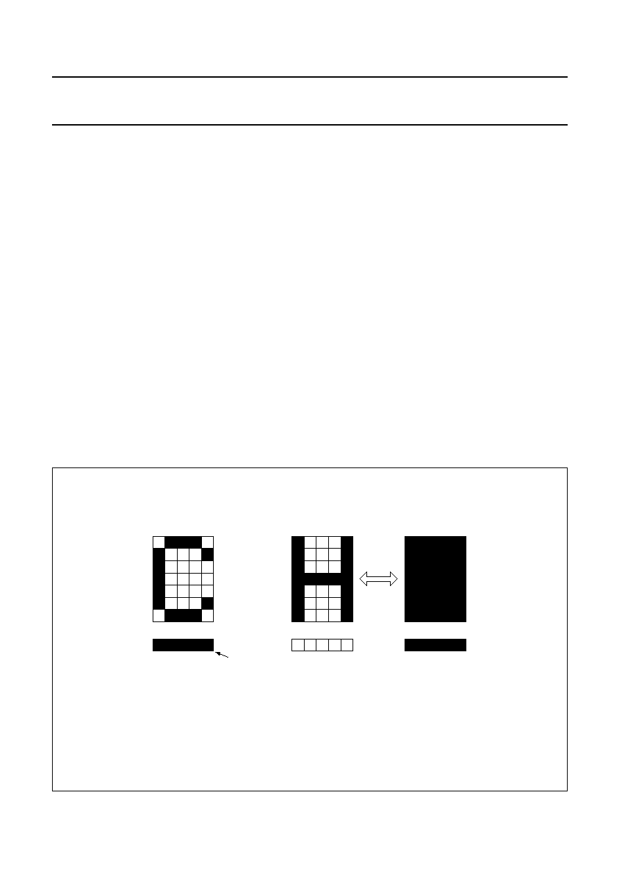
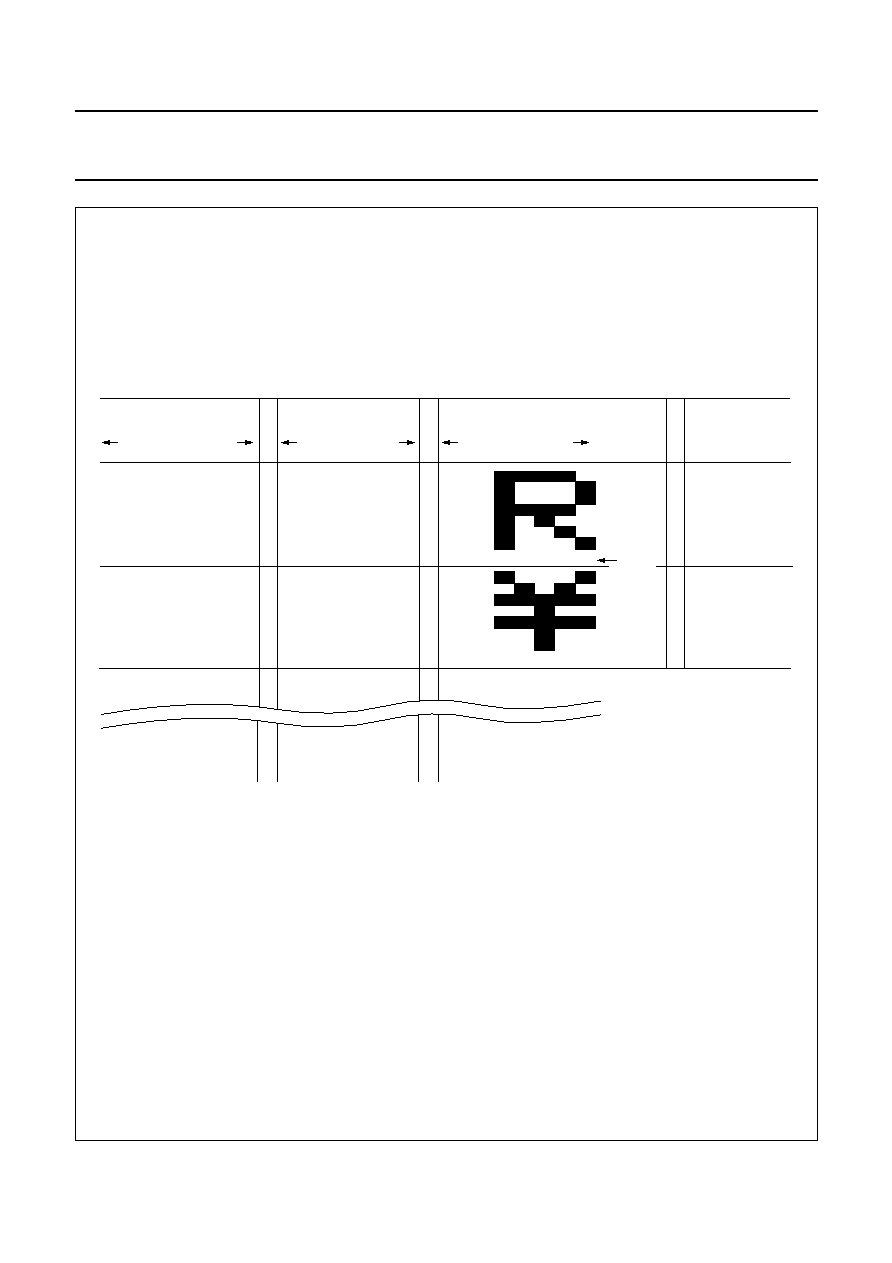
Cursor control circuit
The cursor control circuit generates the cursor underline
and/or cursor blink as shown in Fig.6 at the DDRAM
address contained in the address counter.
When the address counter contains the CGRAM address
the cursor will be inhibited.
7.14
Timing generator
The timing generator produces the various signals
required to drive the internal circuitry. Internal chip
operation is not disturbed by operations on the data buses.
7.15
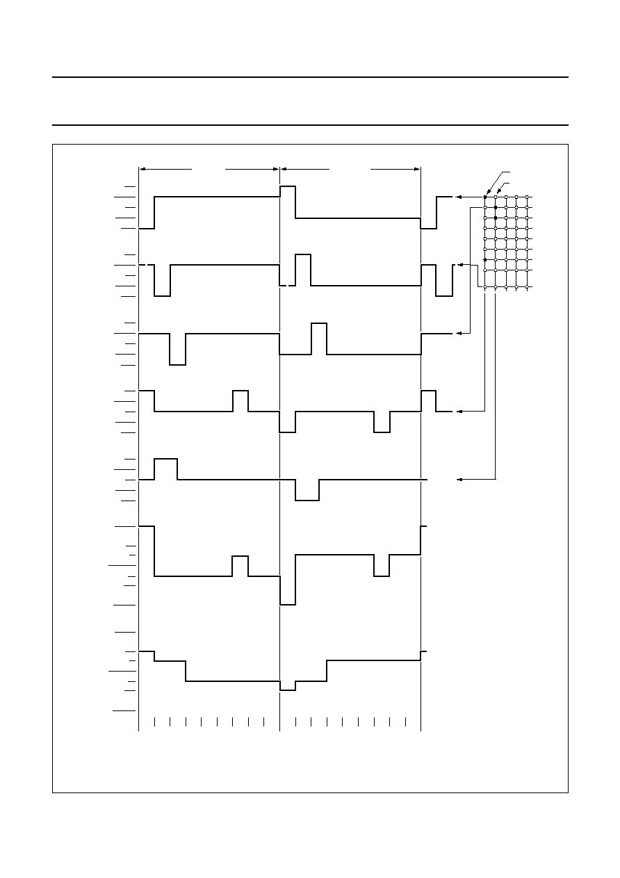
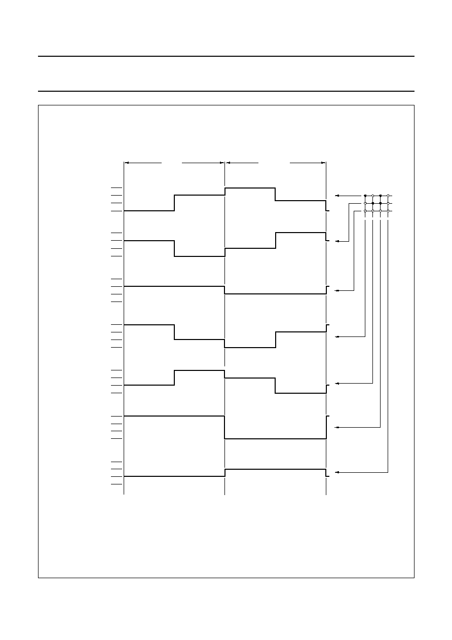
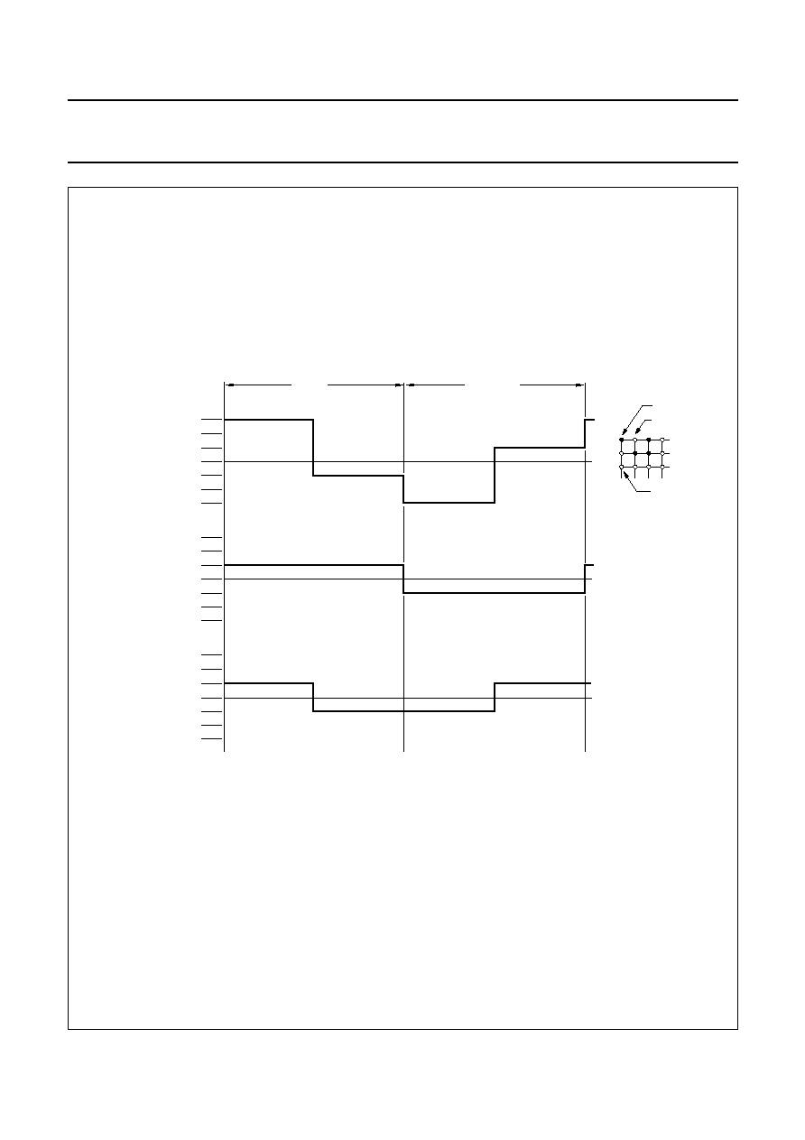
LCD row and column drivers
The PCF2113x contains 18 row and 60 column drivers,
which connect the appropriate LCD bias voltages in
sequence to the display in accordance with the data to be
displayed. R17 and R18 drive the icon rows.
The bias voltages and the timing are selected
automatically when the number of lines in the display is
selected. Figures 12, 13, 14 and 15 show typical
waveforms. Unused outputs should be left unconnected.
MGA801
cursor
5 x 7 dot character font
alternating display
cursor display example
blink display example
Fig.6 Cursor and blink display examples.
2001 Dec 19
13
Philips Semiconductors
Product specification
LCD controllers/drivers
PCF2113x
handbook, full pagewidth
MGE994
0000
0001
0010
0011
0100
0101
0110
0111
1000
1001
1010
1011
1100
1101
1110
1111
upper
4 bits
lower
4 bits
xxxx 0000
xxxx 0001
xxxx 0010
xxxx 0011
xxxx 0100
xxxx 0101
xxxx 0110
xxxx 0111
xxxx 1000
xxxx 1001
xxxx 1010
xxxx 1011
xxxx 1100
xxxx 1101
xxxx 1110
xxxx 1111
16
15
14
13
12
11
10
9
8
7
6
5
4
3
2
1
Fig.7 Character set `A' in CGROM.
2001 Dec 19
14
Philips Semiconductors
Product specification
LCD controllers/drivers
PCF2113x
handbook, full pagewidth
MGD688
0000
0001
0010
0011
0100
0101
0110
0111
1000
1001
1010
1011
1100
1101
1110
1111
upper
4 bits
lower
4 bits
xxxx 0000
xxxx 0001
xxxx 0010
xxxx 0011
xxxx 0100
xxxx 0101
xxxx 0110
xxxx 0111
xxxx 1000
xxxx 1001
xxxx 1010
xxxx 1011
xxxx 1100
xxxx 1101
xxxx 1110
xxxx 1111
16
15
14
13
12
11
10
9
8
7
6
5
4
3
2
1
Fig.8 Character set `D' in CGROM.
2001 Dec 19
15
Philips Semiconductors
Product specification
LCD controllers/drivers
PCF2113x
handbook, full pagewidth
MGD689
0000
0001
0010
0011
0100
0101
0110
0111
1000
1001
1010
1011
1100
1101
1110
1111
upper
4 bits
lower
4 bits
xxxx 0000
xxxx 0001
xxxx 0010
xxxx 0011
xxxx 0100
xxxx 0101
xxxx 0110
xxxx 0111
xxxx 1000
xxxx 1001
xxxx 1010
xxxx 1011
xxxx 1100
xxxx 1101
xxxx 1110
xxxx 1111
16
15
14
13
12
11
10
9
8
7
6
5
4
3
2
1
Fig.9 Character set `E' in CGROM.
2001 Dec 19
16
Philips Semiconductors
Product specification
LCD controllers/drivers
PCF2113x
handbook, full pagewidth
MGU204
0000
0001
0010
0011
0100
0101
0110
0111
1000
1001
1010
1011
1100
1101
1110
1111
upper
4 bits
lower
4 bits
xxxx 0000
xxxx 0001
xxxx 0010
xxxx 0011
xxxx 0100
xxxx 0101
xxxx 0110
xxxx 0111
xxxx 1000
xxxx 1001
xxxx 1010
xxxx 1011
xxxx 1100
xxxx 1101
xxxx 1110
xxxx 1111
16
15
14
13
12
11
10
9
8
7
6
5
4
3
2
1
Fig.10 Character set `W' in CGROM.
2001 Dec 19
17
Philips Semiconductors
Product specification
LCD controllers/drivers
PCF2113x
handbook, full pagewidth
MGE995
7
6
5
4
3
2
1
0
6
5
4
3
2
1
0
4
3
2
1
0
higher
order
bits
lower
order
bits
lower
order
bits
higher
order
bits
lower
order
bits
higher
order
bits
0
0
0
0
0
0
0
0
0
0
0
0
0
0
0
0
0
0
1
0
0
0
0
1
0
0
0
0
0
1
1
0
1
0
0
0
0
0
1
0
1
0
0
0
1
1
0
0
0
0
1
1
1
0
0
0
0
0
0
0
0
0
0
0
0
0
1
0
0
0
0
1
0
0
0
0
0
0
1
1
1
0
0
1
0
1
0
0
0
0
1
1
0
0
0
0
0
1
1
1
0
0
0
0
0
0
0
1
0
0
0
0
0
0
0
1
0
0
0
1
0
0
0
0
0
0
1
0
0
0
0
0
1
1
1
1
0
0
0
0
1
1
1
1
0
0
0
0
1
1
1
1
0
0
0
0
1
1
1
1
0
1
0
0
0
0
0
1
0
0
1
0
1
1
1
0
1
1
1
1
1
1
1
1
1
1
1
1
1
1
1
1
1
1
1
character codes
(DDRAM data)
CGRAM
address
character patterns
(CGRAM data)
4
3
2
1
0
0
0
0
0
1
1
1
0
0
0
0
0
0
1
0
0
0
0
1
0
0
0
1
1
1
0
0
1
1
1
1
1
1
1
1
1
1
0
0
0
1
1
0
1
0
0
0
1
1
1
0
1
1
1
1
0
1
0
0
0
1
0
0
1
0
0
0
0
1
1
0
1
0
0
1
0
0
0
0
0
character code
(CGRAM data)
character
pattern
example 1
cursor
position
character
pattern
example 2
Character code bits 0 to 3 correspond to CGRAM address bits 3 to 6.
CGRAM address bits 0 to 2 designate the character pattern line position. The 8th line is the cursor position and display is performed by logical OR with
the cursor. Data in the 8th position will appear in the cursor position.
Character pattern column positions correspond to CGRAM data bits 0 to 4, as shown in this figure.
As shown in Figs 7 and 8, CGRAM character patterns are selected when character code bits 4 to 7 are all logic 0. CGRAM data = logic 1 corresponds
to selection for display.
Only bits 0 to 5 of the CGRAM address are set by the `set CGRAM address' command. Bit 6 can be set using the `set DDRAM address' command in
the valid address range or by using the auto-increment feature during CGRAM write. All bits 0 to 6 can be read using the `read busy flag' and `address
counter' command.
Fig.11 Relationship between CGRAM addresses, data and display patterns.
2001 Dec 19
18
Philips Semiconductors
Product specification
LCD controllers/drivers
PCF2113x
handbook, full pagewidth
MGE996
state 1 (ON)
state 2 (OFF)
frame n + 1
frame n
1 2 3
18 1 2 3
18
ROW 1
VLCD
V2
V3/V4
V5
VSS
ROW 9
VLCD
V2
V3/V4
V5
VSS
ROW 2
VLCD
V2
V3/V4
V5
VSS
COL1
VLCD
V2
V3/V4
V5
VSS
COL2
VLCD
V2
V3/V4
V5
VSS
0 V
state 1
VOP
0.5VOP
0.25VOP
-
0.25VOP
-
0.5VOP
-
VOP
0 V
state 2
VOP
0.5VOP
0.25VOP
-
0.25VOP
-
0.5VOP
-
VOP
R1
R2
R3
R4
R5
R6
R7
R8
R9
Fig.12 MUX 1 : 18 LCD waveforms; character mode.
2001 Dec 19
19
Philips Semiconductors
Product specification
LCD controllers/drivers
PCF2113x
handbook, full pagewidth
MGU217
state 1 (ON)
state 2 (OFF)
frame n
+
1
frame n
1
2
3
9
1
2
3
9
ROW 1
VLCD
V2
V3/V4
V5
VSS
ROW 2
VLCD
V2
V3/V4
V5
VSS
ROW 3
VLCD
V2
V3/V4
V5
VSS
COL1
VLCD
V2
V3/V4
V5
VSS
COL2
VLCD
V2
V3/V4
V5
VSS
0 V
state 1
VOP
0.5VOP
0.25VOP
-
0.25VOP
-
0.5VOP
-
VOP
0 V
state 2
VOP
0.5VOP
0.25VOP
-
0.25VOP
-
0.5VOP
-
VOP
R1
R2
R3
R4
R5
R6
R7
R8
R9
Fig.13 MUX 1 : 9 LCD waveforms; character mode.
R10 to R18 to be left open.
2001 Dec 19
20
Philips Semiconductors
Product specification
LCD controllers/drivers
PCF2113x
handbook, full pagewidth
MGE997
frame n
+
1
frame n
VLCD
2/3
1/3
VSS
VLCD
2/3
1/3
VSS
VLCD
2/3
1/3
VSS
VLCD
2/3
1/3
VSS
VLCD
2/3
1/3
VSS
VLCD
2/3
1/3
VSS
VLCD
2/3
1/3
VSS
COL 4 OFF/OFF
COL 3 ON/ON
COL 2 OFF/ON
COL 1 ON/OFF
ROW 1 to 16
ROW 18
ROW 17
only icons are
driven (MUX 1 : 2)
Fig.14 MUX 1 : 2 LCD waveforms; icon mode.
2001 Dec 19
21
Philips Semiconductors
Product specification
LCD controllers/drivers
PCF2113x
handbook, full pagewidth
MGE998
frame n
+
1
frame n
VOP
2/3 VOP
1/3 VOP
0
-
1/3 VOP
-
2/3 VOP
-
VOP
VOP
2/3 VOP
1/3 VOP
0
-
1/3 VOP
-
2/3 VOP
-
VOP
VOP
2/3 VOP
1/3 VOP
0
-
1/3 VOP
-
2/3 VOP
-
VOP
state 3
COL 1 -
ROW 1 to 16
state 2
COL 2 -
ROW 17
state 1
COL 1 -
ROW 17
state 3 (OFF)
R17
R18
R1-16
VPIXEL
state 1 (ON)
state 2 (OFF)
Fig.15 MUX 1 : 2 LCD waveforms; icon mode.
V
ON(rms)
= 0.745V
OP
V
OFF(rms)
= 0.333V
OP
D
V
ON
V
OFF
-------------
2.23
=
=
2001 Dec 19
22
Philips Semiconductors
Product specification
LCD controllers/drivers
PCF2113x
7.16
Reset function
The PCF2113x automatically initializes (resets) when power is turned on. The chip executes a reset sequence, including
a `clear display', requiring 165 oscillator cycles. After the reset the chip has the state shown in Table 3.
Table 3
State after reset
STEP
FUNCTION
CONTROL BIT STATE
CONDITIONS
1
clear display
2
entry mode set
I/D = 1
+1 (increment)
S = 0
no shift
3
display control
D = 0
display off
C = 0
cursor off
B = 0
cursor character blink off
4
function set
DL = 1
8-bit interface
M = 0
1-line display
H = 0
normal instruction set
SL = 0
MUX 1 : 18 mode
5
default address pointer to DDRAM; the Busy Flag (BF) indicates the busy state (BF = 1) until
initialization ends; the busy state lasts 2 ms; the chip may also be initialized by software;
see Tables 17 and 18
6
icon control
IM = 0; IB = 0; DM = 0
icons, icon blink and direct
mode disabled
7
display/screen configuration
L = 0; P = 0; Q = 0
default configurations
8
V
LCD
temperature coefficient
TC1 = 0; TC2 = 0
default temperature coefficient
9
set V
LCD
V
A
= 0; V
B
= 0
V
LCD
generator off
10
I
2
C-bus interface reset
11
Set HVgen stages
S1 = 1; S0 = 0
V
LCD
generator voltage
multiplier set at factor 4
2001 Dec 19
23
Philips Semiconductors
Product specification
LCD controllers/drivers
PCF2113x
8
INSTRUCTIONS
Only two PCF2113x registers, the Instruction Register (IR)
and the Data Register (DR) can be directly controlled by
the microcontroller. Before internal operation, control
information is stored temporarily in these registers, to
allow interfacing to various types of microcontrollers which
operate at different speeds or to allow interface to
peripheral control ICs.
The instruction set for I
2
C-bus commands is given in
Table 4.
The PCF2113x operation is controlled by the instructions
shown in Table 5 together with their execution time.
Details are explained in subsequent sections.
Instructions are of 4 types, those that:
1. Designate PCF2113x functions such as display
format, data length, etcetera.
2. Set internal RAM addresses
3. Perform data transfer with internal RAM
4. Others.
In normal use, category 3 instructions are used most
frequently. However, automatic incrementing by 1
(or decrementing by 1) of internal RAM addresses after
each data write lessens the microcontroller program load.
The display shift in particular can be performed
concurrently with display data write, enabling the designer
to develop systems in minimum time with maximum
programming efficiency.
During internal operation, no instructions other than the
`read busy flag' and `read address' instructions will be
executed. Because the busy flag is set to a logic 1 while an
instruction is being executed, check to ensure it is a logic 0
before sending the next instruction or wait for the
maximum instruction execution time, as given in Table 5.
An instruction sent while the busy flag is logic 1 will not be
executed.
Table 4
Instruction set for I
2
C-bus commands
Note
1. R/W is set together with the slave address.
CONTROL BYTE
COMMAND BYTE
I
2
C-BUS COMMANDS
Co
RS 0
0
0
0
0
0
DB7
DB6
DB5
DB4
DB3
DB2
DB1
DB0
note 1
2001
Dec
19
24
Philips Semiconductors
Product specification
LCD controllers/dr
iv
ers
PCF2113x
This text is here in white to force landscape pages to be rotated correctly when browsing through the pdf in the Acrobat reader.This text is here in
_
white to force landscape pages to be rotated correctly when browsing through the pdf in the Acrobat reader.This text is here inThis text is here in
white to force landscape pages to be rotated correctly when browsing through the pdf in the Acrobat reader. white to force landscape pages to be ...
Table 5
Instruction set with parallel bus commands
INSTRUCTION
RS
R/W DB7 DB6 DB5 DB4 DB3 DB2 DB1 DB0
DESCRIPTION
REQUIRE
CLOCK
CYCLES
H = 0 or 1
NOP
0
0
0
0
0
0
0
0
0
0
no operation
3
Function set
0
0
0
0
1
DL
0
M
SL
H
sets interface Data Length (DL), number of display
lines (M), single line/MUX 1 : 9 (SL) and extended
instruction set control (H)
3
Read busy flag
and address
counter
0
1
BF
A
C
reads the Busy Flag (BF) indicating internal
operating is being performed and reads Address
counter (A
C
) contents
0
Read data
1
1
read data
reads data from CGRAM or DDRAM
3
Write data
1
0
write data
writes data from CGRAM or DDRAM
3
H = 0
Clear display
0
0
0
0
0
0
0
0
0
1
clears entire display and sets DDRAM address 0 in
address counter
165
Return home
0
0
0
0
0
0
0
0
1
0
sets DDRAM address 0 in address counter; also
returns shifted display to original position; DDRAM
contents remain unchanged
3
Entry mode set
0
0
0
0
0
0
0
1
I/D
S
sets cursor move direction (I/D) and specifies shift
of display (S); these operations are performed
during data write and read
3
Display control
0
0
0
0
0
0
1
D
C
B
sets entire display on/off (D), cursor on/off (C) and
blink of cursor position character (B); D = 0 (display
off) puts chip into the Power-down mode
3
Cursor/display
shift
0
0
0
0
0
1
S/C
R/L
0
0
moves cursor or shifts display (S/C) to right or left
(R/L) without changing DDRAM contents
3
Set CGRAM
address
0
0
0
1
A
CG
sets CGRAM address; bit DB6 is to be set by the
command `set DDRAM address'; look at the
description of the commands
3
Set DDRAM
address
0
0
1
A
DD
sets DDRAM address
3
2001
Dec
19
25
Philips Semiconductors
Product specification
LCD controllers/dr
iv
ers
PCF2113x
This text is here in white to force landscape pages to be rotated correctly when browsing through the pdf in the Acrobat reader.This text is here in
_
white to force landscape pages to be rotated correctly when browsing through the pdf in the Acrobat reader.This text is here inThis text is here in
white to force landscape pages to be rotated correctly when browsing through the pdf in the Acrobat reader. white to force landscape pages to be ...
H = 1
Reserved
0
0
0
0
0
0
0
0
0
1
do not use
-
Screen
configuration
0
0
0
0
0
0
0
0
1
L
set screen configuration (L)
3
Display
configuration
0
0
0
0
0
0
0
1
P
Q
set display configuration, columns (P) and rows (Q)
3
Icon control
0
0
0
0
0
0
1
IM
IB
DM
set Icon Mode (IM), Icon Blink (IB),
Direct Mode (DM)
3
Temperature
control
0
0
0
0
0
1
0
0
TC1 TC2 set Temperature Coefficient (TCx)
3
Set HVgen stages
0
0
0
1
0
0
0
0
S1
S0
set internal V
LCD
generator voltage multiplier stages
(S1 = 1 and S0 = 1 not allowed)
3
Set V
LCD
0
0
1
V
voltage
store V
LCD
in register V
A
or V
B
(V)
3
INSTRUCTION
RS
R/W DB7 DB6 DB5 DB4 DB3 DB2 DB1 DB0
DESCRIPTION
REQUIRE
CLOCK
CYCLES

2001 Dec 19
26
Philips Semiconductors
Product specification
LCD controllers/drivers
PCF2113x
Table 6
Explanations of symbols used in Tables 4 and 5.
BIT
LOGIC STATE 0
LOGIC STATE 1
Co
last control byte; see Table 4
another control byte follows after data/command
DL
4 bits
8 bits
M (no impact,
if SL = 1)
1-line by 24 display
2-line by 12 display
SL
MUX 1 : 18 (1
◊
24 or 2
◊
12 character display)
MUX 1 : 9 (1
◊
12 character display)
H
use basic instruction set
use extended instruction set
I/D
decrement
increment
S
display freeze
display shift
D
display off
display on
C
cursor off
cursor on
B
cursor character blink off; character at cursor
position does not blink
cursor character blink on; character at cursor
position blinks
S/C
cursor move
display shift
R/L
left shift
right shift
L (no impact,
if M = 1 or
SL = 1)
left/right screen: standard connection
left/right screen; mirrored connection
1st 12 characters of 24; columns are from 1 to 60
1st 12 characters of 24; columns are from 1 to 60
2nd 12 characters of 24; columns are from 1 to 60 2nd 12 characters of 24; columns are from 60 to 1
P
column data: left to right; column data is displayed
from 1 to 60
column data; right to left; column data is displayed
from 60 to 1
Q
row data; top to bottom; row data is displayed from
1 to 16 and icon row data is in 17 and 18
row data; bottom to top; row data is displayed
from 16 to 1 and icon row data is in 18 and 17
IM
character mode; full display
icon mode; only icons displayed
IB
icon blink disabled
icon blink enabled
DM
direct mode disabled
direct mode enabled
V
set V
A
set V
B
8.1
Clear display
`Clear display' writes character code 20H into all DDRAM
addresses (the character pattern for character code 20H
must be a blank pattern), sets the DDRAM address
counter to logic 0 and returns the display to its original
position, if it was shifted. Thus, the display disappears and
the cursor or blink position goes to the left edge of the
display. Sets entry mode I/D = 1 (increment mode). S of
entry mode does not change.
The instruction `clear display' requires extra execution
time. This may be allowed by checking the Busy Flag (BF)
or by waiting until the 165 clock cycles have elapsed.
The latter must be applied where no read-back options are
foreseen, as in some Chip-On-Glass (COG) applications.
8.2
Return home
`Return home' sets the DDRAM address counter to logic 0
and returns the display to its original position if it was
shifted. DDRAM contents do not change. The cursor or
blink position goes to the left of the first display line.
I/D and S of entry mode do not change.

2001 Dec 19
27
Philips Semiconductors
Product specification
LCD controllers/drivers
PCF2113x
8.3
Entry mode set
8.3.1
B
IT
I/D
When I/D = 1 (0) the DDRAM or CGRAM address
increments (decrements) by 1 when data is written into or
read from the DDRAM or CGRAM. The cursor or blink
position moves to the right when incremented and to the
left when decremented. The cursor underline and cursor
character blink are inhibited when the CGRAM is
accessed.
8.3.2
B
IT
S
When S = 1, the entire display shifts either to the right
(I/D = 0) or to the left (I/D = 1) during a DDRAM write. Thus
it appears as if the cursor stands still and the display
moves. The display does not shift when reading from the
DDRAM, or when writing to or reading from the CGRAM.
When S = 0, the display does not shift.
8.4
Display control (and partial Power-down mode)
8.4.1
B
IT
D
The display is on when D = 1 and off when D = 0. Display
data in the DDRAM is not affected and can be displayed
immediately by setting D = 1.
When the display is off (D = 0) the chip is in partial
Power-down mode:
∑
The LCD outputs are connected to V
SS
∑
The LCD generator and bias generator are turned off.
Three oscillator cycles are required after sending the
`display off' instruction to ensure all outputs are at V
SS
,
afterwards the oscillator can be stopped. If the oscillator is
running during partial Power-down mode (`display off') the
chip can still execute instructions. Even lower current
consumption is obtained by inhibiting the oscillator
(OSC = V
SS
).
To ensure I
DD
< 1
µ
A, the parallel bus pins DB7 to DB0
should be connected to V
DD
; pins RS and R/W to V
DD
or
left open-circuit and pin PD to V
DD
. Recovery from
Power-down mode: PD back to V
SS
, if necessary pin OSC
back to V
DD
and send a `display control' instruction with
D = 1.
8.4.2
B
IT
C
The cursor is displayed when C = 1 and inhibited when
C = 0. Even if the cursor disappears, the display functions
I/D, etcetera, remain in operation during display data write.
The cursor is displayed using 5 dots in the 8th line (see
Fig.6).
8.4.3
B
IT
B
The character indicated by the cursor blinks when B = 1.
The cursor character blink is displayed by switching
between display characters and all dots on with a period of
approximately 1 second, with
The cursor underline and the cursor character blink can be
set to display simultaneously.
8.5
Cursor or display shift
`Cursor/display shift' moves the cursor position or the
display to the right or left without writing or reading display
data. This function is used to correct a character or move
the cursor through the display. In 2-line displays, the
cursor moves to the next line when it passes the last
position (40) of the line. When the displayed data is shifted
repeatedly all lines shift at the same time; displayed
characters do not shift into the next line.
The Address Counter (AC) content does not change if the
only action performed is shift display, but increments or
decrements with the `cursor display shift'.
8.6
Function set
8.6.1
B
IT
DL (
PARALLEL MODE ONLY
)
Sets interface data width. Data is sent or received in bytes
(DB7 to DB0) when DL = 1 or in two nibbles (DB7 to DB4)
when DL = 0. When 4-bit width is selected, data is
transmitted in two cycles using the parallel bus. In a 4-bit
application DB3 to DB0 should be left open-circuit (internal
pull-ups). Hence in the first `function set' instruction after
power-on M, SL and H are set to logic 1. A second
`function set' must then be sent (2 nibbles) to set M,
SL and H to their required values.
`Function set' from the I
2
C-bus interface sets the DL bit to
logic 1.
8.6.2
B
IT
M
Selects either 1-line by 24 display (M = 0) or 2-line by
12 display (M = 1).
8.6.3
B
IT
SL
Selects MUX 1 : 9, 1-line by 12 display (independent of
M and L). Only rows 1 to 8 and 17 are to be used. All other
rows must be left open-circuit. The DDRAM map is the
same as in the 2-line by 12 display mode, however, the
second line cannot be displayed.
f
blink
f
OSC
52 224
-----------------
=

2001 Dec 19
28
Philips Semiconductors
Product specification
LCD controllers/drivers
PCF2113x
8.6.4
B
IT
H
When H = 0 the chip can be programmed via the standard
11 instruction codes used in the PCF2116 and other LCD
controllers.
When H = 1 the extended range of instructions will be
used. These are mainly for controlling the display
configuration and the icons.
8.7
Set CGRAM address
`Set CGRAM address' sets bits DB5 to 0 of the CGRAM
address A
CG
into the address counter (binary A5 to A0).
Data can then be written to or read from the CGRAM.
Attention: the CGRAM address uses the same address
register as the DDRAM address and consists of 7 bits
(binary A6 to A0). With the `set CGRAM address'
command, only bits DB5 to DB0 are set. Bit DB6 can be
set using the `set DDRAM address' command first, or by
using the auto-increment feature during CGRAM write. All
bits DB6 to DB0 can be read using the `read busy flag' and
`read address' command.
When writing to the lower part of the CGRAM, ensure that
bit DB6 of the address is not set (e.g. by an earlier DDRAM
write or read action).
8.8
Set DDRAM address
`Set DDRAM address' sets the DDRAM address A
DD
into
the address counter (binary A6 to A0). Data can then be
written to or read from the DDRAM.
8.9
Read busy flag and read address
`Read busy flag and address counter' read the Busy Flag
(BF) and Address Counter (AC). BF = 1 indicates that an
internal operation is in progress. The next instruction will
not be executed until BF = 0. It is recommended that the
BF status is checked before the next write operation is
executed.
At the same time, the value of the address counter
expressed in binary A6 to A0 is read out. The address
counter is used by both CGRAM and DDRAM, and its
value is determined by the previous instruction.
8.10
Write data to CGRAM or DDRAM
`Write data' writes binary 8-bit data DB7 to DB0 to the
CGRAM or the DDRAM.
Whether the CGRAM or DDRAM is to be written into is
determined by the previous `set CGRAM address' or `set
DDRAM address' command. After writing, the address
automatically increments or decrements by 1, in
accordance with the entry mode. Only bits DB4 to DB0 of
CGRAM data are valid, bits DB7 to DB5 are `don't care'.
8.11
Read data from CGRAM or DDRAM
`Read data' reads binary 8-bit data DB7 to DB0 from the
CGRAM or DDRAM.
The most recent `set address' command determines
whether the CGRAM or DDRAM is to be read.
The `read data' instruction gates the content of the Data
Register (DR) to the bus while pin E is HIGH. After pin E
goes LOW again, internal operation increments (or
decrements) the AC and stores RAM data corresponding
to the new AC into the DR.
There are only three instructions that update the data
register:
∑
`Set CGRAM address'
∑
`Set DDRAM address'
∑
`Read data' from CGRAM or DDRAM.
Other instructions (e.g. `write data', `cursor/display shift',
`clear display' and `return home') do not modify the data
register content.
9
EXTENDED FUNCTION SET INSTRUCTIONS AND
FEATURES
9.1
New instructions
H = 1 sets the chip into alternate instruction set mode.
9.2
Icon control
The PCF2113x can drive up to 120 icons. See Fig.16 for
CGRAM to icon mapping.
2001 Dec 19
29
Philips Semiconductors
Product specification
LCD controllers/drivers
PCF2113x
handbook, full pagewidth
COL 1 to 5
1
2
3
4
5
61
62
63
64
65
display:
ROW 17 ≠
ROW 18 ≠
block of 5 columns
COL 6 to 10
6
7
8
9
10
66
67
68
69
70
COL 56 to 60
56
57
58
59
60
116 117 118 119 120
MGE999
handbook, full pagewidth
MGG001
116-120
odd (blink)
18/56-60
0 0 0 0 0 1 1 0
icon view
0 1 1 0 0 1 1
0 0 1 1 0
1-5
odd (blink)
17/1-5
0 0 0 0 0 1 0 0
0 1 0 0 0 0 0
0 0 0 0 0
116-120
even
18/56-60
0 0 0 0 0 0 1 0
0 0 1 0 1 1 1
1 1 1 0 1
61-65
even
18/1-5
0 0 0 0 0 0 0 1
0 0 0 1 1 0 0
1 1 0 0 0
56-60
even
17/56-60
0 0 0 0 0 0 0 1
0 0 0 1 0 1 1
1 1 1 1 1
11-15
even
17/11-15
0 0 0 0 0 0 0 0
0 0 0 0 0 1 0
0 1 1 1 0
6-10
even
17/6-10
0 0 0 0 0 0 0 0
0 0 0 0 0 0 1
0 1 0 1 0
1-5
even
17/1-5
0 0 0 0 0 0 0 0
0 0 0 0 0 0 0
1 0 1 0 1
7 6 5 4 3 2 1 0
MSB
LSB
LSB
MSB
MSB
LSB
6 5 4 3 2 1 0
4 3 2 1 0
icon no.
phase
ROW/COL
character codes
CGRAM address
CGRAM data
Fig.16 CGRAM to icon mapping.
CGRAM data bit = logic 1 turns the icon on, data bit = logic 0 turns the icon off.
Data in character codes 0 to 3 define the icon state when icon blink is disabled or during the even phase when icon blink is enabled.
Data in character codes 4 to 7 define the icon state during the odd phase when icon blink is enabled (not used for icons when icon blink is disabled).
2001 Dec 19
30
Philips Semiconductors
Product specification
LCD controllers/drivers
PCF2113x
9.3
Bit IM
When IM = 0, the chip is in character mode. In the
character mode characters and icons are driven
(MUX 1 : 18). The V
LCD
generator, if used, produces the
V
LCD
voltage programmed in register V
A
.
When IM = 1, the chip is in icon mode. In the icon mode
only the icons are driven (MUX 1 : 2) and the V
LCD
generator, if used, produces the V
LCD
voltage as
programmed in register V
B
.
Table 7
Normal/icon mode operation
9.4
Bit IB
Icon blink control is independent of the cursor/character
blink function.
When IB = 0, the icon blink is disabled. Icon data is stored
in CGRAM character 0 to 2 (3
◊
8
◊
5 = 120 bits for
120 icons).
When IB = 1, the icon blink is enabled. In this case each
icon is controlled by two bits. Blink consists of two half
phases (corresponding to the cursor on and off phases
called even and odd phases hereafter).
Icon states for the even phase are stored in CGRAM
characters 0 to 2 (3
◊
8
◊
5 = 120 bits for 120 icons).
These bits also define icon state when icon blink is not
used (see Table 9).
Icon states for the odd phase are stored in CGRAM
character 4 to 6 (another 120 bits for the 120 icons). When
icon blink is disabled CGRAM characters 4 to 6 may be
used as normal CGRAM characters.
9.5
Direct mode
When DM = 0, the chip is not in the direct mode. Either the
internal V
LCD
generator or an external voltage may be
used to achieve V
LCD
.
When DM = 1, the chip is in direct mode. The internal V
LCD
generator is turned off and the V
LCD2
output is directly
connected to the V
LCD
generator supply voltage V
DD2
.
The direct mode can be used to reduce the current
consumption when the required V
LCD2
output voltage is
close to the V
DD2
supply voltage. This can be the case in
icon mode or in Mux 1:9 (depending on LCD liquid
properties).
9.6
Voltage multiplier control
Bits S1 and S0
A software configurable voltage multiplier is incorporated
in the V
LCD
generator and can be set via the `Set HVgen
stages' command.
The voltage multiplier control can be used to reduce
current consumption by disconnecting internal voltage
multiplier stages, depending on the required V
LCD
output
voltage (see Table 8).
Table 8
S1 and S0 control of voltage multiplier
9.7
Screen configuration
Bit L
L = 0: the two halves of a split screen are connected in a
standard way i.e. column 1/61, 2/62 to 60/120; default.
L = 1: the two halves of a split screen are connected in a
mirrored way i.e. column 1/120, 2/119 to 60/61. This
allows single layer PCB or glass layout.
IM
MODE
V
LCD
0
character mode
generates V
A
1
icon mode
generates V
B
S1
S0
DESCRIPTION
0
0
set V
LCD
generator stages to 1
(2 x voltage multiplier)
0
1
set V
LCD
generator stages to 2
(3 x voltage multiplier)
1
0
set V
LCD
generator stages to 3
(4 x voltage multiplier)
1
1
do not use
Table 9
Blink effect for icons and cursor character blink
PARAMETER
EVEN PHASE
ODD PHASE
Cursor character blink
block (all on)
normal (display character)
Icons
state 1; CGRAM character 0 to 2
state 2; CGRAM character 4 to 6
2001 Dec 19
31
Philips Semiconductors
Product specification
LCD controllers/drivers
PCF2113x
9.8
Display configuration
Bit P
P = 0: default.
P = 1: mirrors the column data.
Bit Q
Q = 0: default.
Q = 1: mirrors the row data.
9.9
Temperature control
Default is TC1 = 0 and TC2 = 0. Selects the default
temperature coefficient for the internally generated V
LCD
(see Table 10).
The ranges for TC are given in Chapter 13.
Table 10 TC1 and TC2 selection of V
LCD
temperature
coefficient
9.10
Set V
LCD
The V
LCD
value is programmed by instruction. Two on-chip
registers, V
A
and V
B
hold V
LCD
values for the character
mode and the icon mode respectively. The generated
V
LCD
value is independent of V
DD
, allowing battery
operation of the chip.
V
LCD
programming:
1. Send `function set' instruction with H = 1
2. Send `set V
LCD
' instruction to write to voltage register:
a) DB7, DB6 = 10: DB5 to DB0 are V
LCD
of character
mode (V
A
)
b) DB7, DB6 = 11: DB5 to DB0 are V
LCD
of icon
mode (V
B
)
c) DB5 to DB0 = 000000 switches V
LCD
generator off
(when selected)
d) During `display off' and power-down the V
LCD
generator is also disabled.
3. Send `function set' instruction with H = 0 to resume
normal programming.
9.11
Reducing current consumption
Reducing current consumption can be achieved by one of
the options given in Table 11.
When V
LCD
lies outside the V
DD
range and must be
generated, it is usually more efficient to use the on-chip
generator than an external regulator.
Table 11 Reducing current consumption
TC1
TC2
DESCRIPTION
0
0
V
LCD
temperature coefficient 0
1
0
V
LCD
temperature coefficient 1
0
1
V
LCD
temperature coefficient 2
1
1
V
LCD
temperature coefficient 3
ORIGINAL MODE
ALTERNATIVE MODE
Character mode
Icon mode (control bit IM)
Display on
Display off (control bit D)
V
LCD
generator operating
Direct mode
Any mode
power-down (PD pin)
2001 Dec 19
32
Philips Semiconductors
Product specification
LCD controllers/drivers
PCF2113x
10 INTERFACES TO MICROCONTROLLER
10.1
Parallel interface
The PCF2113x can send data in either two 4-bit operations
or one 8-bit operation and can thus interface to 4-bit or
8-bit microcontrollers.
In 8-bit mode data is transferred as 8-bit bytes using the
8 data lines DB7 to DB0. Three further control lines E,
RS and R/W are required (see Chapter 6).
In 4-bit mode data is transferred in two cycles of 4 bits
each using pins DB7 to DB4 for the transaction.
The higher order bits (corresponding to DB7 to DB4 in
8-bit mode) are sent in the first cycle and the lower order
bits (DB3 to DB0 in 8-bit mode) in the second cycle. Data
transfer is complete after two 4-bit data transfers. It should
be noted that two cycles are also required for the busy flag
check. 4-bit operation is selected by instruction, see
Figs 17 to 19 for examples of bus protocol.
In 4-bit mode, pins DB3 to DB0 must be left open-circuit.
They are pulled up to V
DD
internally.
10.2
I
2
C-bus interface
The I
2
C-bus is for bidirectional, two-line communication
between different ICs or modules. The two lines are the
Serial Data line (SDA) and the Serial Clock Line (SCL).
Both lines must be connected to a positive supply via
pull-up resistors. Data transfer may be initiated only when
the bus is not busy.
Each byte of eight bits is followed by an acknowledge bit.
The acknowledge bit is a HIGH level signal put on the bus
by the transmitter during which time the master generates
an extra acknowledge related clock pulse. A slave receiver
which is addressed must generate an acknowledge after
the reception of each byte.
Also a master receiver must generate an acknowledge
after the reception of each byte that has been clocked out
of the slave transmitter.
The device that acknowledges must pull-down the SDA
line during the acknowledge clock pulse, so that the SDA
line is stable LOW during the HIGH period of the
acknowledge related clock pulse (set-up and hold times
must be taken into consideration).
MGA804
RS
E
DB7
R/W
DB6
DB5
DB4
instruction
write
busy flag and
address counter read
data register
read
IR7
IR3
BF
AC3
DR7
DR3
IR6
IR2
AC6
AC2
DR6
DR2
IR5
IR1
AC5
AC1
DR5
DR1
IR4
IR0
AC4
AC0
DR4
DR0
Fig.17 4-bit transfer example.
2001 Dec 19
33
Philips Semiconductors
Product specification
LCD controllers/drivers
PCF2113x
MGA805
RS
E
internal
DB7
R/W
internal operation
IR7
IR3
AC3
D7
D3
not
busy
AC3
busy
instruction
write
busy flag
check
busy flag
check
instruction
write
Fig.18 An example of 4-bit data transfer timing sequence.
IR7, IR3: instruction 7th, 3rd bit.
AC3: address counter 3rd bit.
D7, D3: data 7th, 3rd bit.
MGA806
instruction
write
busy flag
check
busy flag
check
busy flag
check
instruction
write
internal operation
RS
E
internal
DB7
R/W
data
busy
busy
not
busy
data
Fig.19 Example of busy flag checking timing sequence.
2001 Dec 19
34
Philips Semiconductors
Product specification
LCD controllers/drivers
PCF2113x
A master receiver must signal an end of data to the
transmitter by not generating an acknowledge bit on the
last byte that has been clocked out of the slave. In this
event the transmitter must leave the data line HIGH to
enable the master to generate a STOP condition.
10.2.1
I
2
C-
BUS PROTOCOL
Before any data is transmitted on the I
2
C-bus, the device
which should respond is addressed first. The addressing is
always carried out with the first byte transmitted after the
START procedure. The I
2
C-bus configuration for the
different PCF2113x read and write cycles is shown in
Figs 24 to 26. The slow down feature of the I
2
C-bus
protocol (receiver holds SCL LOW during internal
operations) is not used in the PCF2113x.
10.2.2
D
EFINITIONS
∑
Transmitter: the device which sends the data to the bus
∑
Receiver: the device which receives the data from the
bus
∑
Master: the device which initiates a transfer generates
clock signals and terminates a transfer
∑
Slave: the device addressed by a master
∑
Multi-master: more than one master can attempt to
control the bus at the same time without corrupting the
message
∑
Arbitration: procedure to ensure that if more than one
master simultaneously tries to control the bus, only one
is allowed to do so and the message is not corrupted
∑
Synchronization: procedure to synchronize the clock
signals of two or more devices.
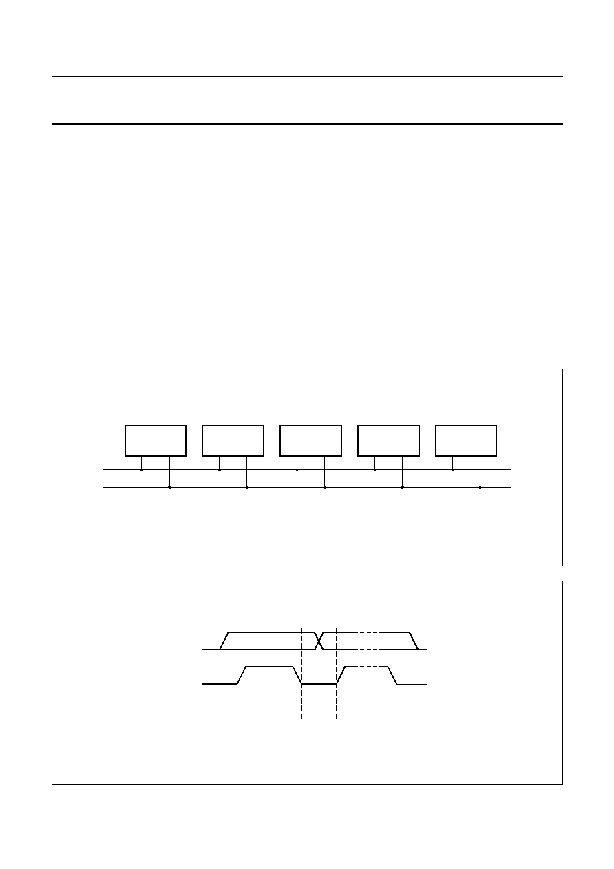
MGA807
SDA
SCL
MASTER
TRANSMITTER/
RECEIVER
MASTER
TRANSMITTER
SLAVE
TRANSMITTER/
RECEIVER
SLAVE
RECEIVER
MASTER
TRANSMITTER/
RECEIVER
Fig.20 System configuration.
handbook, full pagewidth
MBC621
data line
stable;
data valid
change
of data
allowed
SDA
SCL
Fig.21 Bit transfer.
2001 Dec 19
35
Philips Semiconductors
Product specification
LCD controllers/drivers
PCF2113x
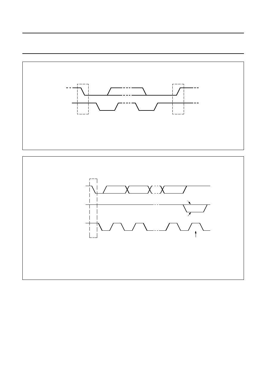
handbook, full pagewidth
MBC622
SDA
SCL
P
STOP condition
SDA
SCL
S
START condition
Fig.22 Definition of START and STOP conditions.
handbook, full pagewidth
MBC602
S
START
condition
9
8
2
1
clock pulse for
acknowledgement
not acknowledge
acknowledge
DATA OUTPUT
BY TRANSMITTER
DATA OUTPUT
BY RECEIVER
SCL FROM
MASTER
Fig.23 Acknowledgement on the I
2
C-bus.
2001
Dec
19
36
Philips Semiconductors
Product specification
LCD controllers/dr
iv
ers
PCF2113x
This text is here in white to force landscape pages to be rotated correctly when browsing through the pdf in the Acrobat reader.This text is here in
_
white to force landscape pages to be rotated correctly when browsing through the pdf in the Acrobat reader.This text is here inThis text is here in
white to force landscape pages to be rotated correctly when browsing through the pdf in the Acrobat reader. white to force landscape pages to be ...
handbook, full pagewidth
MGG002
S
A
0
S
P
0 1 1 1 0 1
0 A
slave address
CONTROL BYTE A
1
Co
DATA BYTE
A
CONTROL BYTE A
R/W
0
Co
update
data pointer
1 byte
n
0 bytes
2n
0 bytes
DATA BYTE
A
acknowledgement
from PCF2113x
RS
RS
S
A
0
0 1 1 1 0 1
0
PCF2113x
slave address
R/W
Fig.24 Master transmits to slave receiver; write mode.
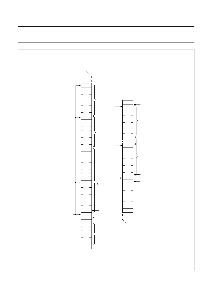
2001
Dec
19
37
Philips Semiconductors
Product specification
LCD controllers/dr
iv
ers
PCF2113x
This text is here in white to force landscape pages to be rotated correctly when browsing through the pdf in the Acrobat reader.This text is here in
_
white to force landscape pages to be rotated correctly when browsing through the pdf in the Acrobat reader.This text is here inThis text is here in
white to force landscape pages to be rotated correctly when browsing through the pdf in the Acrobat reader. white to force landscape pages to be ...
handbook, full pagewidth
MGG003
S
A
0
S
0 1 1 1 0 1
0 A
slave address
CONTROL BYTE A
1
Co
DATA BYTE
A
CONTROL BYTE A
R/W
0
Co
Co
update
data pointer
update
data pointer
1 byte
n
0 bytes
n bytes
last byte
2n 0 bytes
DATA BYTE
(1)
A
acknowledgement
S
A
0
S
1 A
DATA BYTE
A
1
P
SLAVE
ADDRESS
DATA BYTE
acknowledgement
acknowledgement
no acknowledgement
R/W
RS
RS
Fig.25 Master reads after setting word address; writes word address, set RS; `read data'.
Last data byte is a dummy byte (may be omitted).
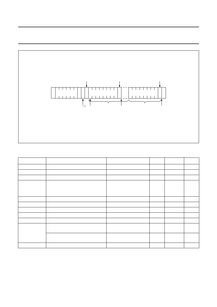
2001 Dec 19
38
Philips Semiconductors
Product specification
LCD controllers/drivers
PCF2113x
handbook, full pagewidth
MGG004
Co
update
data pointer
update
data pointer
n bytes
last byte
S
A
0
S
1 A
DATA BYTE
A
1
P
SLAVE
ADDRESS
DATA BYTE
acknowledgement
from PCF2113x
acknowledgement
from master
no acknowledgement
from master
R/W
Fig.26 Master reads slave immediately after first byte; read mode (RS previously defined).
11 LIMITING VALUES
In accordance with the Absolute Maximum Rating System (IEC 60134).
12 HANDLING INSTRUCTIONS
Inputs and outputs are protected against electrostatic discharge in normal handling. However, to be totally safe, it is
desirable to take normal precautions appropriate to handling MOS devices (see
"Handling MOS Devices").
SYMBOL
PARAMETER
CONDITIONS
MIN.
MAX.
UNIT
V
DD1
logic supply voltage
-
0.5
+5.5
V
V
DD2
, V
DD3
V
LCD
generator supply voltages
-
0.5
+4
V
V
LCD
LCD supply voltage
-
0.5
+6.5
V
V
i/o(n)
voltage on
any V
DD
related input or output
-
0.5
V
DD
+ 0.5
V
any V
LCD
related input or output
-
0.5
V
LCD
+ 0.5
V
I
I
DC input current
-
10
+10
mA
I
O
DC output current
-
10
+10
mA
I
DD
, I
SS
and I
LCD
V
DD
, V
SS
or V
LCD
supply current
-
50
+50
mA
P
tot
total power dissipation
-
400
mW
P
O
power dissipation per output
-
100
mW
V
es
electrostatic handling voltage
human body model;
C = 100 pF; R = 1.5 k
-
2000
V
electrostatic handling voltage
machine model;
C = 200 pF; L = 0.75
µ
H
-
150
V
T
stg
storage temperature
-
65
+150
∞
C
2001 Dec 19
39
Philips Semiconductors
Product specification
LCD controllers/drivers
PCF2113x
13 DC CHARACTERISTICS
V
DD1
= 1.8 to 5.5 V; V
DD2
= V
DD3
= 2.2 to 4.0 V; V
SS
= 0 V; V
LCD
= 2.2 to 6.5 V; T
amb
=
-
40 to +85
∞
C; unless otherwise
specified.
SYMBOL
PARAMETER
CONDITIONS
MIN.
TYP.
MAX.
UNIT
Supplies
V
DD1
logic supply voltage
note 1
1.8
-
5.5
V
V
DD2
, V
DD3
V
LCD
generator supply
voltages
internal V
LCD
generation
(V
DD2
and V
DD3
< V
LCD
)
2.2
-
4.0
V
V
LCD
LCD supply voltage
2.2
-
6.5
V
V
POR
Power-on reset voltage
note 1 and 2
0.9
-
1.6
V
G
ROUND SUPPLY CURRENT
;
EXTERNAL
V
LCD
; note 3
I
SS1
ground supply current 1
-
70
120
µ
A
I
SS3
ground supply current 3
V
DD
= 3 V; V
LCD
= 5 V; note 4
-
45
80
µ
A
I
SS4
ground supply current 4
icon mode; V
DD
= 3 V;
V
LCD
= 2.5 V; note 4
-
25
45
µ
A
I
SS5
ground supply current 5
Power-down mode;
V
DD
= 3 V; V
LCD
= 2.5 V;
DB7 to DB0, RS and R/W = 1;
OSC = 0; PD = 1
-
2
5
µ
A
G
ROUND SUPPLY CURRENT
;
INTERNAL
V
LCD
; notes 3 and 5
I
SS6
ground supply current 6
-
190
400
µ
A
I
SS8
ground supply current 8
V
DD
= 3 V; V
LCD
= 5 V; note 4
-
160
400
µ
A
I
SS9
ground supply current 9
icon mode; V
DD
= 2.5 V;
V
LCD
= 2.5 V; note 4
-
120
-
µ
A
Logic
V
IL
LOW-level input voltage
V
SS1
-
0.3V
DD1
V
V
IH
HIGH-level input voltage
0.7V
DD1
-
V
DD1
V
V
IL(OSC)
LOW-level input voltage on
pin OSC
V
SS1
-
V
DD1
-
1.2
V
V
IH(OSC)
HIGH-level voltage pin OSC
V
DD1
-
0.1
-
V
DD1
V
I
OL(DB)
LOW-level output current on
pins DB7 to DB0
V
OL
= 0.4 V; V
DD1
= 5 V
1.6
4
-
mA
I
OH(DB)
HIGH-level output current on
pins DB7 to DB0
V
OH
= 4 V; V
DD1
= 5 V
-
1
-
8
-
mA
I
pu
pull-up current at
pins DB7 to DB0
V
I
= V
SS1
0.04
0.15
1
µ
A
I
L
leakage current
V
I
= V
DD1
or V
SS1
-
1
-
+1
µ
A
2001 Dec 19
40
Philips Semiconductors
Product specification
LCD controllers/drivers
PCF2113x
Notes
1. Spikes on V
DD1
or V
SS1
which cause V
DD1
-
V
SS1
1.6 V can cause a Power-on reset.
2. Resets all logic when V
DD1
< V
POR
; 3 OSC cycles required.
3. LCD outputs are open-circuit; inputs at V
DD1
or V
SS1
; bus inactive.
4. T
amb
= 25
∞
C; f
OSC
= 200 kHz.
5. LCD outputs are open-circuit; V
LCD
generator is on; load current I
VLCD
= 5
µ
A (at V
LCD
).
6. Tested on sample basis.
7. Resistance of output pins (R1 to R18 and C1 to C60) with a load current of 10
µ
A; outputs measured one at a time;
external V
LCD
= 3 V, V
DD1, 2, 3
= 3 V.
8. LCD outputs open-circuit; external V
LCD
.
I
2
C-bus; pins SDA and SCL
V
IL
LOW-level input voltage
0
-
0.3V
DD1
V
V
IH
HIGH-level input voltage
0.7V
DD1
-
5.5
V
I
LI
input leakage current
V
I
= V
DD1
or V
SS1
-
1
-
+1
µ
A
C
i
input capacitance
note 6
-
5
-
pF
I
OL (SDA)
LOW-level output current on
pin SDA
V
OL
= 0.4 V; V
DD1
> 2 V
3
-
-
mA
V
OL
= 0.2 V
DD1
; V
DD1
< 2 V
2
-
-
mA
LCD outputs
R
O(ROW)
row output resistance of
pins R1 to R18
note 7
-
10
30
k
R
O(COL)
column output resistance of
pins C1 to C60
note 7
-
15
40
k
V
bias(tol)
bias voltage tolerance on
pins R1 to R18 and C1 to C60
note 8
-
20
130
mV
V
LCD2(tol)
V
LCD
voltage tolerance
T
amb
= 25
∞
C; note 5
V
LCD
< 3 V
-
-
160
mV
V
LCD
< 4 V
-
-
200
mV
V
LCD
< 5 V
-
-
260
mV
V
LCD
< 6 V
-
-
340
mV
TC0
V
LCD
temperature coefficient 0
-
-
0.16
-
%/K
TC1
V
LCD
temperature coefficient 1
-
-
0.18
-
%/K
TC2
V
LCD
temperature coefficient 2
-
-
0.21
-
%/K
TC3
V
LCD
temperature coefficient 3
-
-
0.24
-
%/K
SYMBOL
PARAMETER
CONDITIONS
MIN.
TYP.
MAX.
UNIT
2001 Dec 19
41
Philips Semiconductors
Product specification
LCD controllers/drivers
PCF2113x
14 AC CHARACTERISTICS
V
DD1
= 1.8 to 5.5 V; V
DD2
= V
DD3
= 2.2 to 4.0 V; V
SS
= 0 V; V
LCD
= 2.2 to 6.5 V; T
amb
=
-
40 to +85
∞
C; unless otherwise
specified.
SYMBOL
PARAMETER
CONDITIONS
MIN.
TYP.
MAX.
UNIT
f
FR
LCD frame frequency (internal clock)
V
DD
= 5.0 V
45
95
147
Hz
f
osc
oscillator frequency (not available at any pin)
140
250
450
kHz
f
OSC(ext)
external clock frequency
140
-
450
kHz
t
osc(st)
oscillator start-up time after power-down
note 1
-
200
300
µ
s
t
W(PD)
power-down HIGH-level pulse width
1
-
-
µ
s
t
SW(PD)
tolerable spike width on PD pin
note 1
-
-
90
ns
Timing characteristics of parallel interface; note 2
W
RITE OPERATION
(
WRITING DATA FROM MICROCONTROLLER TO
PCF2113
X
); see Fig.27
T
cy(en)
enable cycle time
500
-
-
ns
t
W(en)
enable pulse width
220
-
-
ns
t
su(A)
address set-up time
50
-
-
ns
t
h(A)
address hold time
25
-
-
ns
t
su(D)
data set-up time
60
-
-
ns
t
h(D)
data hold time
25
-
-
ns
R
EAD OPERATION
(
READING DATA FROM
PCF2113
X TO MICROCONTROLLER
); see Fig.28
T
cy(en)
enable cycle time
500
-
-
ns
t
W(en)
enable pulse width
220
-
-
ns
t
su(A)
address set-up time
50
-
-
ns
t
h(A)
address hold time
25
-
-
ns
t
d(D)
data delay time
V
DD1
> 2.2 V
-
-
150
ns
V
DD1
> 1.5 V
-
-
250
ns
t
h(D)
data hold time
5
-
100
ns
Timing characteristics of I
2
C-bus interface; see Fig.29; note 2
f
SCL
SCL clock frequency
-
-
400
kHz
t
LOW
SCL clock LOW period
1.3
-
-
µ
s
t
HIGH
SCL clock HIGH period
0.6
-
-
µ
s
t
SU;DAT
data set-up time
100
-
-
ns
t
HD;DAT
data hold time
0
-
-
ns
t
r
SCL and SDA rise time
note 1 and 3
15 + 0.1 C
b
-
300
ns
t
f
SCL and SDA fall time
note 1 and 3
15 + 0.1 C
b
-
300
ns
C
b
capacitive bus line load
-
-
400
pF
t
SU;STA
set-up time for a repeated START condition
0.6
-
-
µ
s
t
HD;STA
START condition hold time
0.6
-
-
µ
s
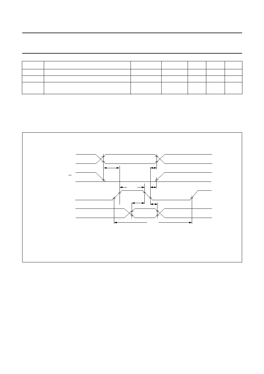
2001 Dec 19
42
Philips Semiconductors
Product specification
LCD controllers/drivers
PCF2113x
Notes
1. Tested on sample base.
2. All timing values are valid within the operating supply voltage and ambient temperature range and are referenced to
V
IL
and V
IH
with an input voltage swing of V
SS
to V
DD
.
3. C
b
= total capacitance of one bus line in pF.
t
SU;STO
set-up time for STOP condition
0.6
-
-
µ
s
t
SW
tolerable spike width on bus
-
-
50
ns
t
BUF
bus free time between STOP and START
condition
1.3
-
-
µ
s
SYMBOL
PARAMETER
CONDITIONS
MIN.
TYP.
MAX.
UNIT
handbook, full pagewidth
RS
E
DB0 to DB7
V
V
V
V
V
V
V
V
V
V
V
V
V
T
IH1
IL1
IH1
IL1
IH1
IL1
IL1
IL1
IH1
IL1
IH1
IL1
VIL1
VIH1
IL1
cy(en)
t su(D)
h(D)
t
tW(en)
th(A)
th(A)
t su(A)
valid data
MBK474
R/W
Fig.27 Parallel bus write operation sequence; writing data from microcontroller to PCF2113x.
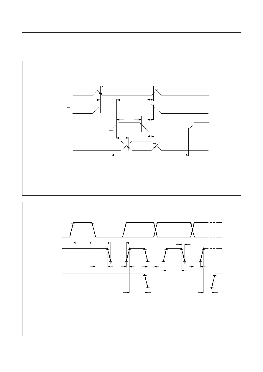
2001 Dec 19
43
Philips Semiconductors
Product specification
LCD controllers/drivers
PCF2113x
handbook, full pagewidth
RS
R/W
E
DB0 to DB7
V
V
V
V
V
V
V
V
V
V
IH1
IL1
IH1
IL1
IH1
IL1
IH1
IL1
VOL1
VOH1
IL1
Tcy(en)
h(D)
t
tW(en)
t h(A)
th(A)
tsu(A)
IH1
VOL1
VOH1
t d(D)
VIH1
MBK475
Fig.28 Parallel bus read operation sequence; writing data from PCF2113x to microcontroller.
handbook, full pagewidth
SDA
MGA728
SDA
SCL
t SU;STA
t
SU;STO
t
HD;STA
t BUF
t LOW
t HD;DAT
t HIGH
t r
t f
t SU;DAT
Fig.29 I
2
C-bus timing diagram.
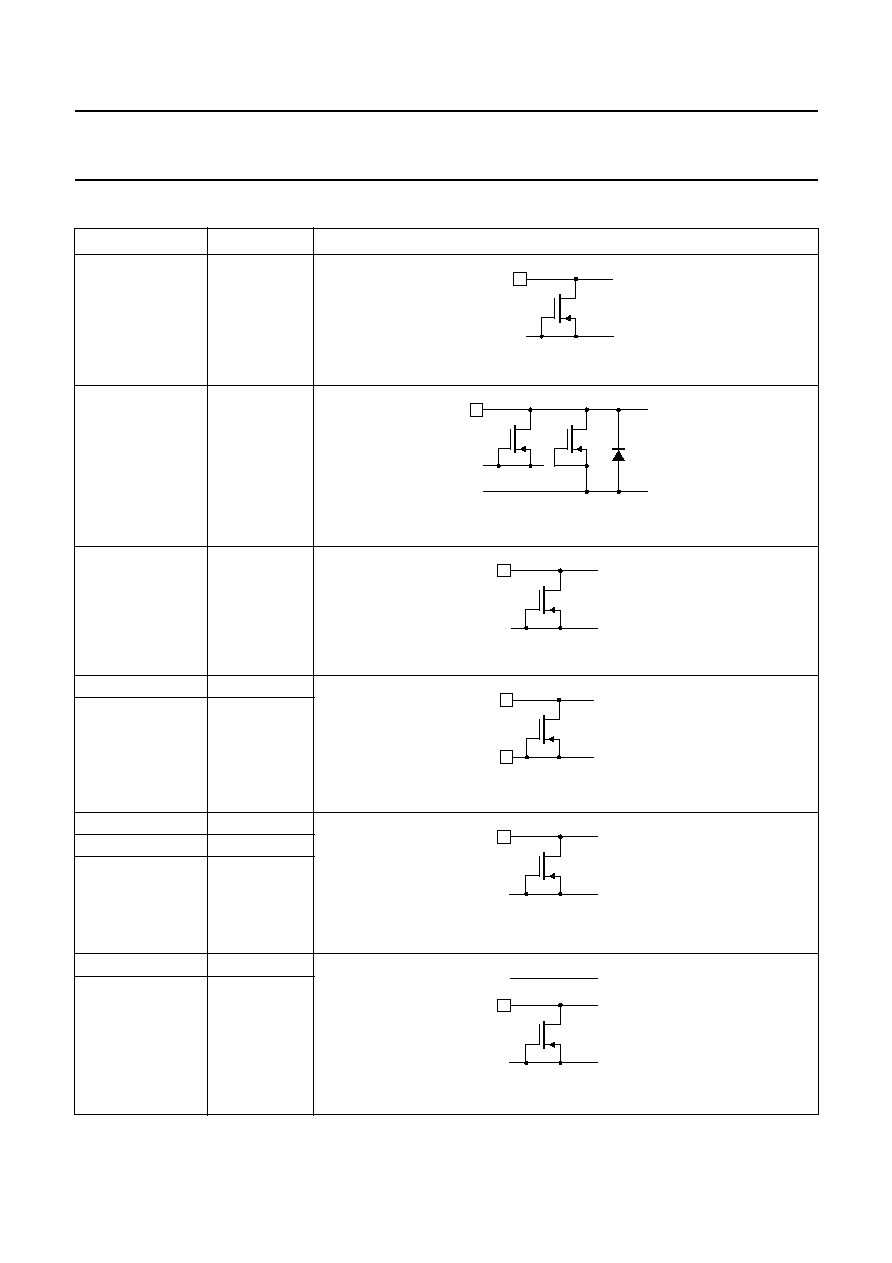
2001 Dec 19
44
Philips Semiconductors
Product specification
LCD controllers/drivers
PCF2113x
15 DEVICE PROTECTION CIRCUITS
SYMBOL
PAD
INTERNAL CIRCUIT
V
DD1
1
V
DD2
109
V
DD3
110
V
SS1
7
V
SS2
8
V
LCDSENSE
10
V
LCD1
11
V
LCD2
9
SCL
96
SDA
97
VSS1
VDD1
MGU200
VSS2
VSS1
VDD2
MGU201
VSS1
VDD3
MGU202
VSS1
VSS2
8
7
MGU203
VSS1
MGU196
VSS1
VDD1
MGU198
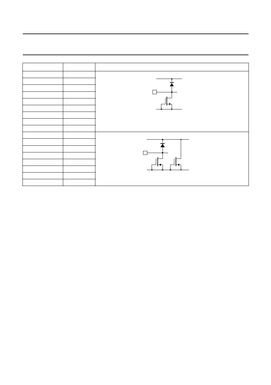
2001 Dec 19
45
Philips Semiconductors
Product specification
LCD controllers/drivers
PCF2113x
OSC
2
PD
3
T1
5
T2
6
T3
4
E
98
RS
99
R/W
100
DB0 to DB7
108 to 101
R1 to R8
94 to 87
R9 to R16
12 to 19
R17
95
R18
20
C1 to C2
86 to 85
C3 to 27
82 to 58
C28 to C52
55 to 31
C53 to C60
28 to 21
SYMBOL
PAD
INTERNAL CIRCUIT
VSS1
MGU199
VDD1
VSS1
MGU197
VLCD2
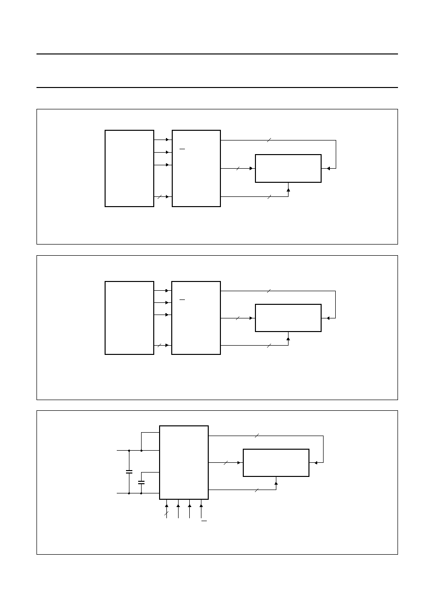
2001 Dec 19
46
Philips Semiconductors
Product specification
LCD controllers/drivers
PCF2113x
16 APPLICATION INFORMATION
handbook, full pagewidth
PCF2113x
MGG006
P80CL51
2
◊
12 CHARACTER
LCD DISPLAY
PLUS 120 ICONS
16
4
C1 to C60
60
2
RS
P10
P11
E
P12
DB7 to DB4
P17 to P14
R17, R18
R1 to R16
R/W
Fig.30 Direct connection to 8-bit microcontroller; 4-bit bus.
handbook, full pagewidth
PCF2113x
MGG005
P80CL51
2
◊
12 CHARACTER
LCD DISPLAY
PLUS 120 ICONS
16
8
C1 to C60
60
2
RS
P20
P21
E
P22
DB7 to DB0
P17 to P10
R17, R18
R1 to R16
R/W
Fig.31 Direct connection to 8-bit microcontroller; 8-bit bus.
handbook, full pagewidth
MGG007
PCF2113x
2
◊
12 CHARACTER
LCD DISPLAY
PLUS 120 ICONS
16
8
C1 to C60
60
2
OSC
RS
DB7 to DB0 E
100
nF
100
nF
R17, R18
R1 to R16
VDD
VSS
VDD
VLCD
VSS
R/W
Fig.32 Typical application using parallel interface.
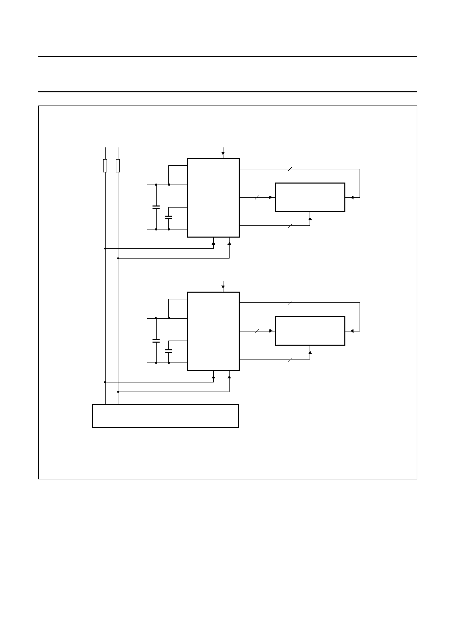
2001 Dec 19
47
Philips Semiconductors
Product specification
LCD controllers/drivers
PCF2113x
handbook, full pagewidth
VDD
VDD
SCL SDA
MASTER TRANSMITTER
PCF84C81A; P80CL410
PCF2113x
2
◊
12 CHARACTER
LCD DISPLAY
PLUS 120 ICONS
16
C1 to C60
60
2
OSC
SCL SDA
DB3/SAO
100
nF
100
nF
R17, R18
R1 to R16
VDD
VDD
VSS
VDD
VLCD
VSS
PCF2113x
1
◊
24 CHARACTER
LCD DISPLAY
PLUS 120 ICONS
16
C1 to C60
60
2
OSC
SCL SDA
DB3/SAO
470
nF
100
nF
R17, R18
R1 to R16
VSS
VDD
VSS
VDD
VLCD
VSS
MGG008
Fig.33 Application using I
2
C-bus interface.
16.1
General application information
The required minimum value for the external capacitors in
an application with the PCF2113x are: C
Ext
for
V
LCD
/V
SS
= 100 nF min., for V
DD
/V
SS
= 470 nF. Higher
capacitor values are recommended for ripple reduction.
For COG applications the recommended ITO track
resistance is to be minimized for the I/O and supply
connections.
Optimized values for these tracks are below 50
for the
supply and below 100
for the I/O connections. Higher
track resistance reduce performance and increase current
consumption.
To avoid accidental triggering of Power-on reset
(especially in COG applications), the supplies must be
adequately decoupled. Depending on power supply
quality, V
DD1
may have to be risen above the specified
minimum.
2001 Dec 19
48
Philips Semiconductors
Product specification
LCD controllers/drivers
PCF2113x
16.2
4-bit operation, 1-line display using internal
reset
The program must set functions prior to a 4-bit operation
(see Table 12). When power is turned on, 8-bit operation
is automatically selected and the PCF2113x attempts to
perform the first write as an 8-bit operation. Since nothing
is connected to DB0 to DB3, a rewrite is then required.
However, since one operation is completed in two
accesses of 4-bit operation, a rewrite is required to set the
functions (see Table 12 step 3). Thus, DB4 to DB7 of the
`function set' are written twice.
16.3
8-bit operation, 1-line display using internal
reset
Tables 13 and 14 show an example of a 1-line display in
8-bit operation. The PCF2113x functions must be set by
the `function set' instruction prior to display. Since the
DDRAM can store data for 80 characters, the RAM can be
used for advertising displays when combined with display
shift operation. Since the display shift operation changes
display position only and the DDRAM contents remain
unchanged, display data entered first can be displayed
when the `return home' operation is performed.
16.4
8-bit operation, 2-line display
For a 2-line display the cursor automatically moves from
the first to the second line after the 40th digit of the first line
has been written. Thus, if there are only 8 characters in the
first line, the DDRAM address must be set after the 8th
character is completed (see Table 15). It should be noted
that both lines of the display are always shifted together;
data does not shift from one line to the other.
16.5
I
2
C-bus operation, 1-line display
A control byte is required with most commands
(see Table 16).
Table 12 4-bit operation, 1-line display example using internal reset
STEP
INSTRUCTION
DISPLAY
OPERATION
1
power supply on (PCF2113x is initialized by
the internal reset)
initialized; no display appears
2
function set
RS
R/W
DB7
DB6
DB5
DB4
sets to 4-bit operation; in this instance operation
is handled as 8-bits by initialization and only this
instruction completes with one write
0
0
0
0
1
0
3
function set
0
0
0
0
1
0
sets to 4-bit operation, selects 1-line display and
V
LCD
= V
0
; 4-bit operation starts from this point
and resetting is needed
0
0
0
0
0
0
4
display control
0
0
0
0
0
0
_
turns on display and cursor; entire display is
blank after initialization
0
0
1
1
1
0
5
entry mode set
0
0
0
0
0
0
_
sets mode to increment the address by 1 and to
shift the cursor to the right at the time of write to
the DD/CGRAM; display is not shifted
0
0
0
1
1
0
6
`write data' to CGRAM/DDRAM
1
0
0
1
0
1
P_
writes `P'; the DDRAM has already been selected
by initialization at power-on; the cursor is
incremented by 1 and shifted to the right
1
0
0
0
0
0

2001
Dec
19
49
Philips Semiconductors
Product specification
LCD controllers/dr
iv
ers
PCF2113x
This text is here in white to force landscape pages to be rotated correctly when browsing through the pdf in the Acrobat reader.This text is here in
_
white to force landscape pages to be rotated correctly when browsing through the pdf in the Acrobat reader.This text is here inThis text is here in
white to force landscape pages to be rotated correctly when browsing through the pdf in the Acrobat reader. white to force landscape pages to be ...
Table 13 8-bit operation, 1-line display example; using internal reset (character set `A')
STEP
INSTRUCTION
DISPLAY
OPERATION
1
power supply on (PCF2113x is initialized by the internal
reset)
initialized; no display appears
2
function set
RS
R/W DB7 DB6 DB5 DB4 DB3 DB2 DB1 DB0
sets to 8-bit operation, selects 1-line display and
V
LCD
= V
0
0
0
0
0
1
1
0
0
0
0
3
display control
0
0
0
0
0
0
1
1
1
0
_
turns on display and cursor; entire display is blank after
initialization
4
entry mode set
0
0
0
0
0
0
0
1
1
0
_
sets mode to increment the address by 1 and to shift the
cursor to the right at the time of the write to the
DD/CGRAM; display is not shifted
5
`write data' to CGRAM/DDRAM
1
0
0
1
0
1
0
0
0
0
P_
writes `P'; the DDRAM has already been selected by
initialization at power-on; the cursor is incremented by 1
and shifted to the right
6
`write data' to CGRAM/DDRAM
1
0
0
1
0
0
1
0
0
0
PH_
writes `H'
7 to 10
|
|
writes `ILIP'
11
`write data' to CGRAM/DDRAM
1
0
0
1
0
1
0
0
1
1
PHILIPS_
writes `S'
12
entry mode set
0
0
0
0
0
0
0
1
1
1
PHILIPS_
sets mode for display shift at the time of write
13
`write data' to CGRAM/DDRAM
1
0
0
0
1
0
0
0
0
0
HILIPS _
writes space
14
`write data' to CGRAM/DDRAM
1
0
0
1
0
0
1
1
0
1
ILIPS
M_
writes `M'
15 to 19
|
|
writes `ICROK'
20
`write data' to CGRAM/DDRAM
1
0
0
1
0
0
1
1
1
1
MICROKO_
writes `O'
2001
Dec
19
50
Philips Semiconductors
Product specification
LCD controllers/dr
iv
ers
PCF2113x
This text is here in white to force landscape pages to be rotated correctly when browsing through the pdf in the Acrobat reader.This text is here in
_
white to force landscape pages to be rotated correctly when browsing through the pdf in the Acrobat reader.This text is here inThis text is here in
white to force landscape pages to be rotated correctly when browsing through the pdf in the Acrobat reader. white to force landscape pages to be ...
21
cursor/display shift
0
0
0
0
0
1
0
0
0
0
MICROKO
shifts only the cursor position to the left
22
cursor/display shift
0
0
0
0
0
1
0
0
0
0
MICROKO
shifts only the cursor position to the left
23
`write data' to CGRAM/DDRAM
1
0
0
1
0
0
0
0
1
1
ICROCO
writes `C' correction; the display moves to the left
24
cursor/display shift
0
0
0
0
0
1
1
1
0
0
MICROCO
shifts the display and cursor to the right
25
cursor/display shift
0
0
0
0
0
1
0
1
0
0
MICROCO_
shifts only the cursor to the right
26
`write data' to CGRAM/DDRAM
1
0
0
1
0
0
1
1
0
1
ICROCOM_
writes `M'
27
return home
0
0
0
0
0
0
0
0
1
0
PHILIPS M
returns both display and cursor to the original position
(address 0)
STEP
INSTRUCTION
DISPLAY
OPERATION
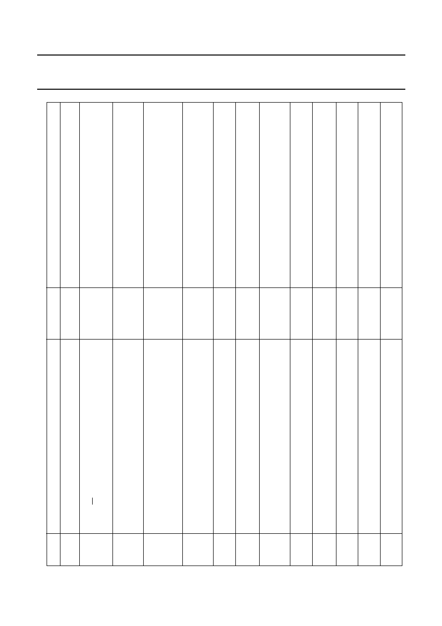
2001
Dec
19
51
Philips Semiconductors
Product specification
LCD controllers/dr
iv
ers
PCF2113x
This text is here in white to force landscape pages to be rotated correctly when browsing through the pdf in the Acrobat reader.This text is here in
_
white to force landscape pages to be rotated correctly when browsing through the pdf in the Acrobat reader.This text is here inThis text is here in
white to force landscape pages to be rotated correctly when browsing through the pdf in the Acrobat reader. white to force landscape pages to be ...
Table 14 8-bit operation, 1-line display and icon example; using internal reset (character set `A')
STEP
INSTRUCTION
DISPLAY
OPERATION
1
power supply on (PCF2113x is initialized by the internal
reset)
initialized; no display appears
2
function set
RS
R/W DB7 DB6 DB5 DB4 DB3 DB2 DB1 DB0
sets to 8-bit operation, selects 1-line display and
V
LCD
= V
0
0
0
0
0
1
1
0
0
0
0
3
display mode on/off control
0
0
0
0
0
0
1
1
1
0
_
turns on display and cursor; entire display is blank after
initialization
4
entry mode set
0
0
0
0
0
0
0
1
1
0
_
sets mode to increment the address by 1 and to shift the
cursor to the right at the time of the write to the
DD/CGRAM; display is not shifted
5
set CGRAM address
0
0
0
1
0
0
0
0
0
0
_
sets the CGRAM address to position of character 0;
the CGRAM is selected
6
`write data' to CGRAM/DDRAM
1
0
0
0
0
0
1
0
1
0
_
writes data to CGRAM for icon even phase; icons appears
7
|
|
8
set CGRAM address
0
0
0
1
1
1
0
0
0
0
_
sets the CGRAM address to position of character 4;
the CGRAM is selected
9
`write data' to CGRAM/DDRAM
1
0
0
0
0
0
1
0
1
0
_
writes data to CGRAM for icon odd phase
10
|
|
11
function set
0
0
0
0
1
1
0
0
0
1
_
sets H = 1
12
icon control
0
0
0
0
0
0
1
0
1
0
_
icons blink
13
function set
0
0
0
0
1
1
0
0
0
1
_
sets H = 0
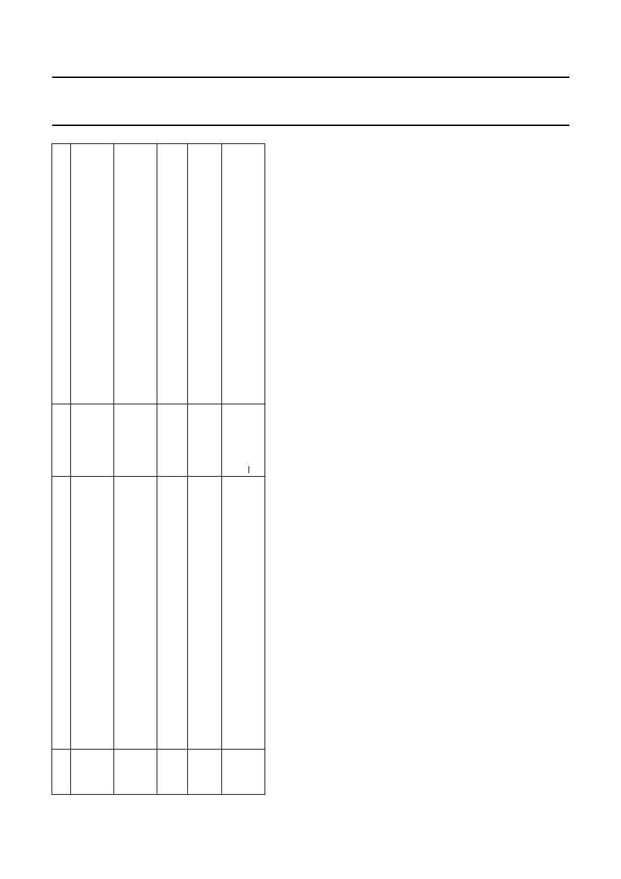
2001
Dec
19
52
Philips Semiconductors
Product specification
LCD controllers/dr
iv
ers
PCF2113x
This text is here in white to force landscape pages to be rotated correctly when browsing through the pdf in the Acrobat reader.This text is here in
_
white to force landscape pages to be rotated correctly when browsing through the pdf in the Acrobat reader.This text is here inThis text is here in
white to force landscape pages to be rotated correctly when browsing through the pdf in the Acrobat reader. white to force landscape pages to be ...
14
set DDRAM address
0
0
1
0
0
0
0
0
0
0
sets the DDRAM address to the first position; DDRAM is
selected
15
`write data' to CGRAM/DDRAM
1
0
0
1
0
1
0
0
0
0
P_
writes `P'; the cursor is incremented by 1 and shifted to
the right
16
`write data' to CGRAM/DDRAM
1
0
0
1
0
0
1
0
0
0
PH_
writes `H'
17 to 21
|
|
writes `ILIPS'
22
return home
0
0
0
0
0
0
0
0
1
0
PHILIPS
returns both display and cursor to the original position
(address 0)
STEP
INSTRUCTION
DISPLAY
OPERATION

2001
Dec
19
53
Philips Semiconductors
Product specification
LCD controllers/dr
iv
ers
PCF2113x
This text is here in white to force landscape pages to be rotated correctly when browsing through the pdf in the Acrobat reader.This text is here in
_
white to force landscape pages to be rotated correctly when browsing through the pdf in the Acrobat reader.This text is here inThis text is here in
white to force landscape pages to be rotated correctly when browsing through the pdf in the Acrobat reader. white to force landscape pages to be ...
Table 15 8-bit operation, 2-line display example; using internal reset
STEP
INSTRUCTION
DISPLAY
OPERATION
1
power supply on (PCF2113x is initialized by the internal
reset)
initialized; no display appears
2
function set
RS
R/W DB7 DB6 DB5 DB4 DB3 DB2 DB1 DB0
sets to 8-bit operation; selects 2-line display and V
LCD
generator off
0
0
0
0
1
1
0
1
0
0
3
display on/off control
0
0
0
0
0
0
1
1
1
0
_
turns on display and cursor; entire display is blank after
initialization
4
entry mode set
0
0
0
0
0
0
0
1
1
0
_
sets mode to increment the address by 1 and to shift the
cursor to the right at the time of write to the CG/DDRAM;
display is not shifted
5
`write data' to CGRAM/DDRAM
1
0
0
1
0
1
0
0
0
0
P_
writes `P'; the DDRAM has already been selected by
initialization at power-on; the cursor is incremented by 1
and shifted to the right
6 to 10
|
|
writes `HILIP'
11
`write data' to CGRAM/DDRAM
1
0
0
1
0
1
0
0
1
1
PHILIPS_
writes `S'
12
set DDRAM address
0
0
1
1
0
0
0
0
0
0
PHILIPS
_
sets DDRAM address to position the cursor at the head of
the 2nd line
13
`write data' to CGRAM/ DDRAM
1
0
0
1
0
0
1
1
0
1
PHILIPS
M_
writes `M'
14 to 18
|
|
writes `ICROC'
19
`write data' to CGRAM/DDRAM
1
0
0
1
0
0
1
1
1
1
PHILIPS
MICROCO_
writes `O'
2001
Dec
19
54
Philips Semiconductors
Product specification
LCD controllers/dr
iv
ers
PCF2113x
This text is here in white to force landscape pages to be rotated correctly when browsing through the pdf in the Acrobat reader.This text is here in
_
white to force landscape pages to be rotated correctly when browsing through the pdf in the Acrobat reader.This text is here inThis text is here in
white to force landscape pages to be rotated correctly when browsing through the pdf in the Acrobat reader. white to force landscape pages to be ...
20
`write data' to CGRAM/DDRAM
0
0
0
0
0
0
0
1
1
1
PHILIPS
MICROCO_
sets mode for display shift at the time of write
21
`write data' to CGRAM/DDRAM
1
0
0
1
0
0
1
1
0
1
HILIPS
ICROCOM_
writes `M'; display is shifted to the left; the first and second
lines shift together
23
return home
0
0
0
0
0
0
0
0
1
0
PHILIPS
MICROCOM
returns both display and cursor to the original position
(address 0)
STEP
INSTRUCTION
DISPLAY
OPERATION
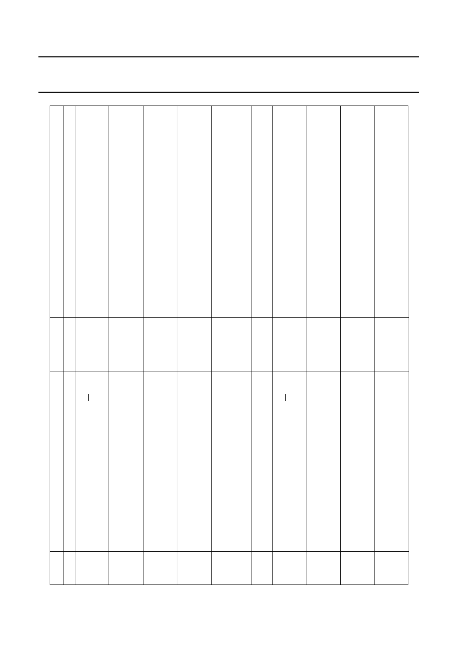
2001
Dec
19
55
Philips Semiconductors
Product specification
LCD controllers/dr
iv
ers
PCF2113x
This text is here in white to force landscape pages to be rotated correctly when browsing through the pdf in the Acrobat reader.This text is here in
_
white to force landscape pages to be rotated correctly when browsing through the pdf in the Acrobat reader.This text is here inThis text is here in
white to force landscape pages to be rotated correctly when browsing through the pdf in the Acrobat reader. white to force landscape pages to be ...
Table 16 Example of I
2
C-bus operation; 1-line display (using internal reset, assuming SA0 = V
SS
; note 1)
STEP
I
2
C-BUS BYTE
DISPLAY
OPERATION
1
I
2
C-bus start
initialized; no display appears
2
slave address for write
SA6 SA5 SA4 SA3 SA2 SA1 SA0 R/W Ack
during the acknowledge cycle SDA will be pulled-down by the
PCF2113x
0
1
1
1
0
1
0
0
1
3
send a control byte for `function set'
Co
RS
0
0
0
0
0
0
Ack
control byte sets RS for following data bytes
0
0
0
0
0
0
0
0
1
4
function set
DB7 DB6 DB5 DB4 DB3 DB2 DB1 DB0 Ack
selects 1-line display and V
LCD
= V
0
; SCL pulse during
acknowledge cycle starts execution of instruction
0
0
1
X
0
0
0
0
1
5
display on/off control
DB7 DB6 DB5 DB4 DB3 DB2 DB1 DB0 Ack
_
turns on display and cursor; entire display shows character 20H
(blank in ASCII-like character sets)
0
0
0
0
1
1
1
0
1
6
entry mode set
DB7 DB6 DB5 DB4 DB3 DB2 DB1 DB0 Ack
_
sets mode to increment the address by 1 and to shift the cursor
to the right at the time of write to the DDRAM or CGRAM; display
is not shifted
0
0
0
0
0
1
1
0
1
7
I
2
C-bus start
_
for writing data to DDRAM, RS must be set to 1; therefore a
control byte is needed
8
slave address for write
SA6 SA5 SA4 SA3 SA2 SA1 SA0 R/W Ack
_
0
1
1
1
0
1
0
0
1
9
send a control byte for `write data'
Co
RS
0
0
0
0
0
0
Ack
_
0
1
0
0
0
0
0
0
1
10
`write data' to DDRAM
DB7 DB6 DB5 DB4 DB3 DB2 DB1 DB0 Ack
P_
writes `P'; the DDRAM has been selected at power-up; the
cursor is incremented by 1 and shifted to the right
0
1
0
1
0
0
0
0
1
11
`write data' to DDRAM
DB7 DB6 DB5 DB4 DB3 DB2 DB1 DB0 Ack
PH_
writes `H'
0
1
0
0
1
0
0
0
1
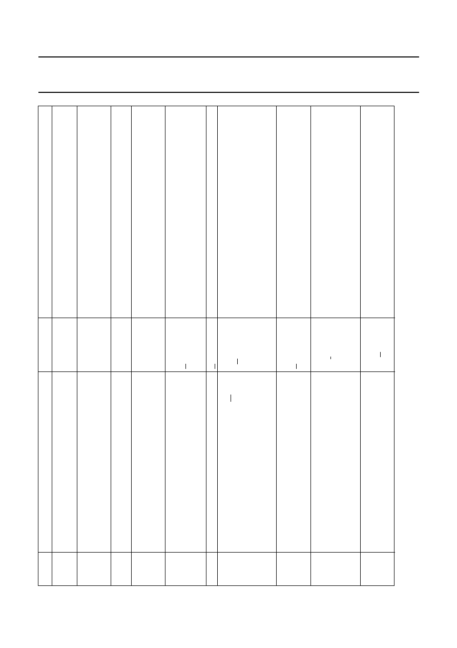
2001
Dec
19
56
Philips Semiconductors
Product specification
LCD controllers/dr
iv
ers
PCF2113x
This text is here in white to force landscape pages to be rotated correctly when browsing through the pdf in the Acrobat reader.This text is here in
_
white to force landscape pages to be rotated correctly when browsing through the pdf in the Acrobat reader.This text is here inThis text is here in
white to force landscape pages to be rotated correctly when browsing through the pdf in the Acrobat reader. white to force landscape pages to be ...
12 to 15
|
|
16
`write data' to DDRAM
DB7 DB6 DB5 DB4 DB3 DB2 DB1 DB0 Ack
PHILIPS_
writes `S'
0
1
0
1
0
0
1
1
1
17
(optional I
2
C-bus stop) I
2
C-bus start start + slave
address for write (as step 8)
PHILIPS_
18
control byte
Co
RS
0
0
0
0
0
0
Ack
PHILIPS_
1
0
0
0
0
0
0
0
1
19
return home
DB7 DB6 DB5 DB4 DB3 DB2 DB1 DB0 Ack
PHILIPS
sets DDRAM address 0 in address counter (also returns shifted
display to original position; DDRAM contents unchanged); this
instruction does not update the Data Register (DR)
0
0
0
0
0
0
1
0
1
20
I
2
C-bus start
PHILIPS
21
slave address for read
SA6 SA5 SA4 SA3 SA2 SA1 SA0 R/W Ack
PHILIPS
during the acknowledge cycle the content of the DR is loaded
into the internal I
2
C-bus interface to be shifted out; in the
previous instruction neither a `set address' nor a `read data' has
been performed; therefore the content of the DR was unknown;
the R/W has to be set to 1 while still in I
2
C-write mode
0
1
1
1
0
1
0
1
1
22
control byte for read
Co
RS
0
0
0
0
0
0
Ack
PHILIPS
DDRAM content will be read from following instructions
0
1
1
0
0
0
0
0
1
23
`read data': 8
◊
SCL + master acknowledge; note 2
DB7 DB6 DB5 DB4 DB3 DB2 DB1 DB0 Ack
PHILIPS
8
◊
SCL; content loaded into interface during previous
acknowledge cycle is shifted out over SDA; MSB is DB7; during
master acknowledge content of DDRAM address 01 is loaded
into the I
2
C-bus interface
X
X
X
X
X
X
X
X
0
24
`read data': 8
◊
SCL + master acknowledge; note 2
DB7 DB6 DB5 DB4 DB3 DB2 DB1 DB0 Ack
PHILIPS
8
◊
SCL; code of letter `H' is read first; during master
acknowledge code of `I' is loaded into the I
2
C-bus interface
0
1
0
0
1
0
0
0
0
STEP
I
2
C-BUS BYTE
DISPLAY
OPERATION
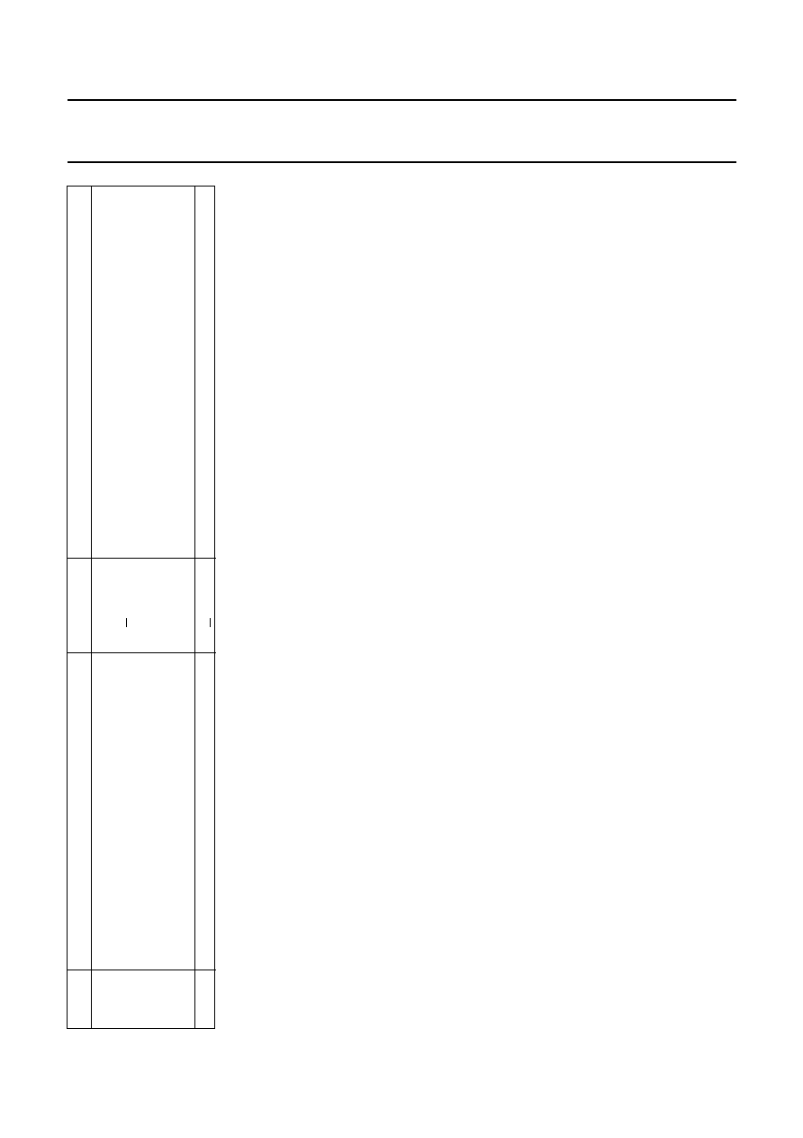
2001
Dec
19
57
Philips Semiconductors
Product specification
LCD controllers/dr
iv
ers
PCF2113x
This text is here in white to force landscape pages to be rotated correctly when browsing through the pdf in the Acrobat reader.This text is here in
_
white to force landscape pages to be rotated correctly when browsing through the pdf in the Acrobat reader.This text is here inThis text is here in
white to force landscape pages to be rotated correctly when browsing through the pdf in the Acrobat reader. white to force landscape pages to be ...
Notes
1. X = don't care.
2. SDA is left at high-impedance by the microcontroller during the read acknowledge.
25
`read data': 8
◊
SCL + no master acknowledge; note 2
DB7 DB6 DB5 DB4 DB3 DB2 DB1 DB0 Ack
PHILIPS
no master acknowledge; after the content of the I
2
C-bus
interface register is shifted out no internal action is performed;
no new data is loaded to the interface register, data register is
not updated, address counter is not incremented and cursor is
not shifted
0
1
0
0
1
0
0
1
1
26
I
2
C-bus stop
PHILIPS
STEP
I
2
C-BUS BYTE
DISPLAY
OPERATION
2001
Dec
19
58
Philips Semiconductors
Product specification
LCD controllers/dr
iv
ers
PCF2113x
This text is here in white to force landscape pages to be rotated correctly when browsing through the pdf in the Acrobat reader.This text is here in
_
white to force landscape pages to be rotated correctly when browsing through the pdf in the Acrobat reader.This text is here inThis text is here in
white to force landscape pages to be rotated correctly when browsing through the pdf in the Acrobat reader. white to force landscape pages to be ...
Table 17 Initialization by instruction, 8-bit interface (note 1)
Note
1. X = don't care.
STEP
DESCRIPTION
power-on or unknown state
|
wait 2 ms after internal reset has been applied
|
RS
R/W
DB7
DB6
DB5
DB4
DB3
DB2
DB1
DB0
BF cannot be checked before this instruction
0
0
0
0
1
1
X
X
X
X
function set (interface is 8 bits long)
|
wait 2 ms
|
RS
R/W
DB7
DB6
DB5
DB4
DB3
DB2
DB1
DB0
BF cannot be checked before this instruction
0
0
0
0
1
1
X
X
X
X
function set (interface is 8 bits long)
|
wait more than 40
µ
s
|
RS
R/W
DB7
DB6
DB5
DB4
DB3
DB2
DB1
DB0
BF cannot be checked before this instruction
0
0
0
0
1
1
X
X
X
X
function set (interface is 8 bits long)
|
|
BF can be checked after the following instructions; when BF is not checked,
the waiting time between instructions is the specified instruction time
(see Table 3)
RS
R/W
DB7
DB6
DB5
DB4
DB3
DB2
DB1
DB0
function set (interface is 8 bits long); specify the number of display lines
0
0
0
0
1
1
0
M
0
H
0
0
0
0
0
0
1
0
0
0
display off
0
0
0
0
0
0
0
0
0
1
clear display
0
0
0
0
0
0
0
1
I/D
S
entry mode set
|
Initialization ends
2001
Dec
19
59
Philips Semiconductors
Product specification
LCD controllers/dr
iv
ers
PCF2113x
This text is here in white to force landscape pages to be rotated correctly when browsing through the pdf in the Acrobat reader.This text is here in
_
white to force landscape pages to be rotated correctly when browsing through the pdf in the Acrobat reader.This text is here inThis text is here in
white to force landscape pages to be rotated correctly when browsing through the pdf in the Acrobat reader. white to force landscape pages to be ...
Table 18 Initialization by instruction, 4-bit interface; not applicable for I
2
C-bus operation
STEP
DESCRIPTION
power-on or unknown state
|
Wait 2 ms after internal reset has been applied
|
RS
R/W
DB7
DB6
DB5
DB4
BF cannot be checked before this instruction
0
0
0
0
1
1
function set (interface is 8 bits long)
|
Wait 2 ms
|
RS
R/W
DB7
DB6
DB5
DB4
BF cannot be checked before this instruction
0
0
0
0
1
1
function set (interface is 8 bits long)
|
Wait 40
µ
s
|
RS
R/W
DB7
DB6
DB5
DB4
BF cannot be checked before this instruction
0
0
0
0
1
1
function set (interface is 8 bits long)
|
BF can be checked after the following instructions; when BF is not checked, the waiting time
between instructions is the specified instruction time (see Table 3)
RS
R/W
DB7
DB6
DB5
DB4
function set (set interface to 4 bits long)
0
0
0
0
1
0
interface is 8 bits long
0
0
0
0
1
0
function set (interface is 4 bits long)
0
0
0
M
0
H
specify number of display lines
0
0
0
0
0
0
0
0
1
0
0
0
display off
0
0
0
0
0
0
clear display
0
0
0
0
0
1
0
0
0
0
0
0
entry mode set
0
0
0
1
I/D
S
|
Initialization ends
2001 Dec 19
60
Philips Semiconductors
Product specification
LCD controllers/drivers
PCF2113x
17 BONDING PAD INFORMATION
SYMBOL
PAD
COORDINATES
(1)
X
Y
V
DD1
1
-
1345
-
1550
OSC
2
-
1155
-
1550
PD
3
-
1 055
-
1550
T3
4
-
845
-
1550
T1
5
-
765
-
1550
T2
6
-
665
-
1550
V
SS1
7
-
525
-
1550
V
SS2
8
-
455
-
1550
V
LCD2
9
-
295
-
1550
V
LCDSENSE
10
-
145
-
1550
V
LCD1
11
+15
-
1550
R9
12
+175
-
1550
R10
13
+245
-
1550
R11
14
+315
-
1550
R12
15
+385
-
1550
R13
16
+455
-
1550
R14
17
+525
-
1550
R15
18
+595
-
1550
R16
19
+665
-
1550
R18
20
+735
-
1550
C60
21
+805
-
1550
C59
22
+875
-
1550
C58
23
+995
-
1550
C57
24
+1065
-
1550
C56
25
+1135
-
1550
C55
26
+1205
-
1550
C54
27
+1275
-
1550
C53
28
+1345
-
1550
dummy pad 1
29
+1435
-
1550
dummy pad 2
30
+1630
-
1395
C52
31
+1630
-
1255
C51
32
+1630
-
1155
C50
33
+1630
-
1055
C49
34
+1630
-
955
C48
35
+1630
-
735
C47
36
+1630
-
635
C46
37
+1630
-
535
C45
38
+1630
-
435
C44
39
+1630
-
335
C43
40
+1630
-
235
C42
41
+1630
-
135
C41
42
+1630
-
35
C40
43
+1630
+65
C39
44
+1630
+165
C38
45
+1630
+265
C37
46
+1630
+365
C36
47
+1630
+465
C35
48
+1630
+565
C34
49
+1630
+665
C33
50
+1630
+765
C32
51
+1630
+865
C31
52
+1630
+965
C30
53
+1630
+1065
C29
54
+1630
+1165
C28
55
+1630
+1265
dummy pad 3
56
+1630
+1335
dummy pad 4
57
+1435
+1550
C27
58
+1335
+1550
C26
59
+1225
+1550
C25
60
+1115
+1550
C24
61
+1005
+1550
C23
62
+765
+1550
C22
63
+665
+1550
C21
64
+565
+1550
C20
65
+465
+1550
C19
66
+365
+1550
C18
67
+265
+1550
C17
68
+165
+1550
C16
69
+65
+1550
C15
70
-
35
+1550
C14
71
-
135
+1550
C13
72
-
235
+1550
C12
73
-
335
+1550
C11
74
-
435
+1550
C10
75
-
535
+1550
C9
76
-
635
+1550
C8
77
-
735
+1550
C7
78
-
835
+1550
C6
79
-
965
+1550
C5
80
-
1065
+1550
C4
81
-
1165
+1550
C3
82
-
1265
+1550
dummy pad 5
83
-
1465
+1550
dummy pad 6
84
-
1630
+1355
C2
85
-
1630
+1255
SYMBOL
PAD
COORDINATES
(1)
X
Y
2001 Dec 19
61
Philips Semiconductors
Product specification
LCD controllers/drivers
PCF2113x
Note
1. All x and y coordinates are referenced to centre of chip
and dimensions are in
µ
m (see Fig.34).
C1
86
-
1630
+1185
R8
87
-
1630
+1115
R7
88
-
1630
+1045
R6
89
-
1630
+975
R5
90
-
1630
+905
R4
91
-
1630
+835
R3
92
-
1630
+765
R2
93
-
1630
+695
R1
94
-
1630
+625
R17
95
-
1630
+555
SCL
96
-
1630
+375
SDA
97
-
1630
+305
E
98
-
1630
+85
RS
99
-
1630
-
15
R/W
100
-
1630
-
115
SYMBOL
PAD
COORDINATES
(1)
X
Y
DB7
101
-
1630
-
215
DB6
102
-
1630
-
315
DB5
103
-
1630
-
415
DB4
104
-
1630
-
515
DB3
105
-
1630
-
615
DB2
106
-
1630
-
715
DB1
107
-
1630
-
815
DB0
108
-
1630
-
915
V
DD2
109
-
1630
-
1015
V
DD3
110
-
1630
-
1235
dummy pad 7
111
-
1630
-
1395
dummy pad 8
112
-
1465
-
1550
SYMBOL
PAD
COORDINATES
(1)
X
Y
2001 Dec 19
62
Philips Semiconductors
Product specification
LCD controllers/drivers
PCF2113x
handbook, full pagewidth
MGU205
dummy pad 6
C2
109
108
107
106
105
104
103
102
101
100
99
98
97
96
95
94
93
92
91
90
89
88
87
86
85
84
30
31
32
33
34
35
36
37
38
39
40
41
42
43
44
45
46
47
48
49
50
51
52
53
54
55
56
57
58
59
60
62
63
64
65
66
67
68
69
70
71
72
73
74
75
76
77
78
79
80
81
82
83
61
110
111
112
1
2
3
4
5
6
7
8
9
10
11
12
13
14
15
16
17
18
19
20
21
22
23
24
25
26
27
28
29
C1
R8
R7
R6
R5
R4
R3
R2
R1
R17
E
RS
RW
DB7
DB6
DB5
DB4
DB3
DB2
DB1
DB0
dummy pad 8
V
DD1
OSC
PD
T3
T1
T2
R9
R10
R11
R12
R13
R14
R15
R16
R18
C60
C59
C58
C57
C56
C55
C54
C53
dummy pad 1
V
SS1
V
SS2
V
LCD2
V
LCD1
V
LCDSENSE
VDD2
VDD3
dummy pad 7
SCL
SDA
dummy pad 2
dummy pad 3
C52
C51
C50
C49
C48
C47
C46
C45
C44
C43
C42
C41
C40
C39
C38
C37
C36
C35
C34
C33
C32
C31
C30
C29
C28
dummy pad 4
C27
C26
C25
C24
C23
C22
C21
C20
C19
C18
C17
C16
C15
C14
C13
C12
C11
C10
C9
C8
C7
C6
C5
C4
C3
dummy pad 5
PC2113x
x
y
0
0
3.36
mm
3.52 mm
Fig.34 Bonding pad locations.
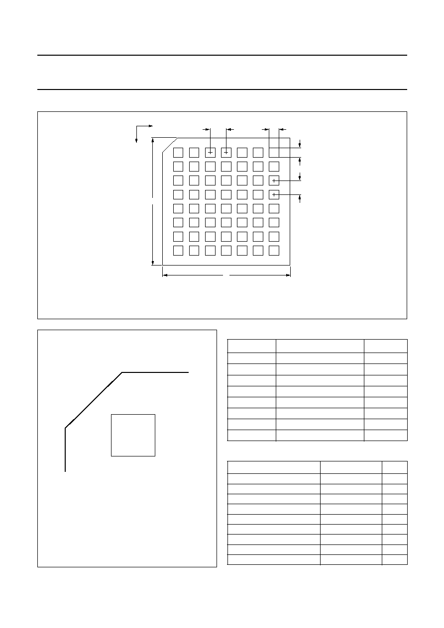
2001 Dec 19
63
Philips Semiconductors
Product specification
LCD controllers/drivers
PCF2113x
18 TRAY INFORMATION
Fig.35 Tray details.
handbook, full pagewidth
MGU206
D
C
A
x
y
F
E
B
For dimensions see Table 19.
Table 19 Tray dimensions
Table 20 Bump size
handbook, halfpage
MGU207
PC2113x
Fig.36 Tray alignment.
The orientation of the IC in a pocket is indicated by the position of the
IC type name on the die surface with respect to the chamfer on the
upper left corner of the tray. Refer to the bonding pad location
diagram for the orientating and position of the type name on the die
surface.
DIMENSION
DESCRIPTION
VALUE
A
pocket pitch x direction
6.35 mm
B
pocket pitch y direction
5.59 mm
C
pocket width x direction
3.82 mm
D
pocket width y direction
3.66 mm
E
tray width x direction
50.8 mm
F
tray width y direction
50.8 mm
x
pockets in x direction
7
y
pockets in y direction
8
PARAMETER
VALUE
UNIT
Type
galvanic pure Au
-
Bump width
50
±
6
µ
m
Bump length
90
±
6
µ
m
Bump height
17.5
±
5
µ
m
Height difference in one die
<2
µ
m
Convex deformation
<5
µ
m
Pad size, aluminium
62
◊
100
µ
m
Passivation opening CBB
36
◊
76
µ
m
Wafer thickness
380
±
25
µ
m
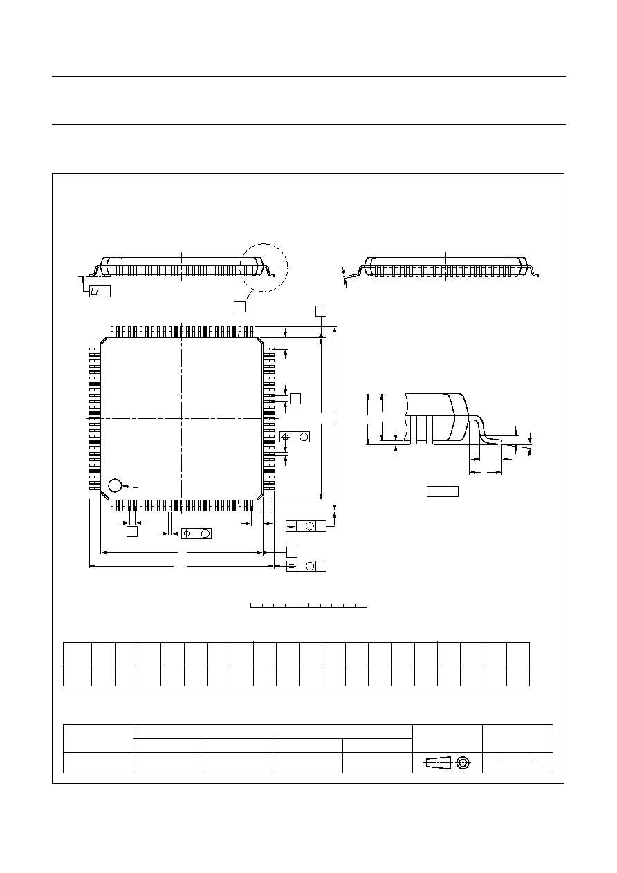
2001 Dec 19
64
Philips Semiconductors
Product specification
LCD controllers/drivers
PCF2113x
19 PACKAGE OUTLINE
UNIT
A
max.
A
1
A
2
A
3
b
p
c
E
(1)
e
H
E
L
L
p
Z
y
w
v
REFERENCES
OUTLINE
VERSION
EUROPEAN
PROJECTION
ISSUE DATE
IEC
JEDEC
EIAJ
mm
1.6
0.15
0.05
1.45
1.35
0.25
0.27
0.17
0.20
0.09
14.1
13.9
0.5
16.25
15.75
1.15
0.85
7
0
o
o
0.08
0.08
0.2
1.0
DIMENSIONS (mm are the original dimensions)
Note
1. Plastic or metal protrusions of 0.25 mm maximum per side are not included.
0.75
0.45
SOT407-1
136E20
MS-026
00-01-19
00-02-01
D
(1)
(1)
(1)
14.1
13.9
H
D
16.25
15.75
E
Z
1.15
0.85
D
b
p
e
E
A
1
A
L
p
detail X
L
(A )
3
B
25
c
D
H
b
p
E
H
A
2
v
M
B
D
ZD
A
Z E
e
v
M
A
X
1
100
76
75
51
50
26
y
pin 1 index
w
M
w
M
0
5
10 mm
scale
LQFP100: plastic low profile quad flat package; 100 leads; body 14 x 14 x 1.4 mm
SOT407-1

2001 Dec 19
65
Philips Semiconductors
Product specification
LCD controllers/drivers
PCF2113x
20 SOLDERING
20.1
Introduction to soldering surface mount
packages
This text gives a very brief insight to a complex technology.
A more in-depth account of soldering ICs can be found in
our
"Data Handbook IC26; Integrated Circuit Packages"
(document order number 9398 652 90011).
There is no soldering method that is ideal for all surface
mount IC packages. Wave soldering can still be used for
certain surface mount ICs, but it is not suitable for fine pitch
SMDs. In these situations reflow soldering is
recommended.
20.2
Reflow soldering
Reflow soldering requires solder paste (a suspension of
fine solder particles, flux and binding agent) to be applied
to the printed-circuit board by screen printing, stencilling or
pressure-syringe dispensing before package placement.
Several methods exist for reflowing; for example,
convection or convection/infrared heating in a conveyor
type oven. Throughput times (preheating, soldering and
cooling) vary between 100 and 200 seconds depending
on heating method.
Typical reflow peak temperatures range from
215 to 250
∞
C. The top-surface temperature of the
packages should preferable be kept below 220
∞
C for
thick/large packages, and below 235
∞
C for small/thin
packages.
20.3
Wave soldering
Conventional single wave soldering is not recommended
for surface mount devices (SMDs) or printed-circuit boards
with a high component density, as solder bridging and
non-wetting can present major problems.
To overcome these problems the double-wave soldering
method was specifically developed.
If wave soldering is used the following conditions must be
observed for optimal results:
∑
Use a double-wave soldering method comprising a
turbulent wave with high upward pressure followed by a
smooth laminar wave.
∑
For packages with leads on two sides and a pitch (e):
≠ larger than or equal to 1.27 mm, the footprint
longitudinal axis is preferred to be parallel to the
transport direction of the printed-circuit board;
≠ smaller than 1.27 mm, the footprint longitudinal axis
must be parallel to the transport direction of the
printed-circuit board.
The footprint must incorporate solder thieves at the
downstream end.
∑
For packages with leads on four sides, the footprint must
be placed at a 45
∞
angle to the transport direction of the
printed-circuit board. The footprint must incorporate
solder thieves downstream and at the side corners.
During placement and before soldering, the package must
be fixed with a droplet of adhesive. The adhesive can be
applied by screen printing, pin transfer or syringe
dispensing. The package can be soldered after the
adhesive is cured.
Typical dwell time is 4 seconds at 250
∞
C.
A mildly-activated flux will eliminate the need for removal
of corrosive residues in most applications.
20.4
Manual soldering
Fix the component by first soldering two
diagonally-opposite end leads. Use a low voltage (24 V or
less) soldering iron applied to the flat part of the lead.
Contact time must be limited to 10 seconds at up to
300
∞
C.
When using a dedicated tool, all other leads can be
soldered in one operation within 2 to 5 seconds between
270 and 320
∞
C.

2001 Dec 19
66
Philips Semiconductors
Product specification
LCD controllers/drivers
PCF2113x
20.5
Suitability of surface mount IC packages for wave and reflow soldering methods
Notes
1. All surface mount (SMD) packages are moisture sensitive. Depending upon the moisture content, the maximum
temperature (with respect to time) and body size of the package, there is a risk that internal or external package
cracks may occur due to vaporization of the moisture in them (the so called popcorn effect). For details, refer to the
Drypack information in the
"Data Handbook IC26; Integrated Circuit Packages; Section: Packing Methods".
2. These packages are not suitable for wave soldering as a solder joint between the printed-circuit board and heatsink
(at bottom version) can not be achieved, and as solder may stick to the heatsink (on top version).
3. If wave soldering is considered, then the package must be placed at a 45
∞
angle to the solder wave direction.
The package footprint must incorporate solder thieves downstream and at the side corners.
4. Wave soldering is only suitable for LQFP, TQFP and QFP packages with a pitch (e) equal to or larger than 0.8 mm;
it is definitely not suitable for packages with a pitch (e) equal to or smaller than 0.65 mm.
5. Wave soldering is only suitable for SSOP and TSSOP packages with a pitch (e) equal to or larger than 0.65 mm; it is
definitely not suitable for packages with a pitch (e) equal to or smaller than 0.5 mm.
PACKAGE
SOLDERING METHOD
WAVE
REFLOW
(1)
BGA, LFBGA, SQFP, TFBGA
not suitable
suitable
HBCC, HLQFP, HSQFP, HSOP, HTQFP, HTSSOP, SMS
not suitable
(2)
suitable
PLCC
(3)
, SO, SOJ
suitable
suitable
LQFP, QFP, TQFP
not recommended
(3)(4)
suitable
SSOP, TSSOP, VSO
not recommended
(5)
suitable

2001 Dec 19
67
Philips Semiconductors
Product specification
LCD controllers/drivers
PCF2113x
21 DATA SHEET STATUS
Note
1. Please consult the most recently issued data sheet before initiating or completing a design.
DATA SHEET STATUS
PRODUCT
STATUS
DEFINITIONS
(1)
Objective specification
Development
This data sheet contains the design target or goal specifications for
product development. Specification may change in any manner without
notice.
Preliminary specification
Qualification
This data sheet contains preliminary data, and supplementary data will be
published at a later date. Philips Semiconductors reserves the right to
make changes at any time without notice in order to improve design and
supply the best possible product.
Product specification
Production
This data sheet contains final specifications. Philips Semiconductors
reserves the right to make changes at any time without notice in order to
improve design and supply the best possible product.
22 DEFINITIONS
Short-form specification
The data in a short-form
specification is extracted from a full data sheet with the
same type number and title. For detailed information see
the relevant data sheet or data handbook.
Limiting values definition
Limiting values given are in
accordance with the Absolute Maximum Rating System
(IEC 60134). Stress above one or more of the limiting
values may cause permanent damage to the device.
These are stress ratings only and operation of the device
at these or at any other conditions above those given in the
Characteristics sections of the specification is not implied.
Exposure to limiting values for extended periods may
affect device reliability.
Application information
Applications that are
described herein for any of these products are for
illustrative purposes only. Philips Semiconductors make
no representation or warranty that such applications will be
suitable for the specified use without further testing or
modification.
23 DISCLAIMERS
Life support applications
These products are not
designed for use in life support appliances, devices, or
systems where malfunction of these products can
reasonably be expected to result in personal injury. Philips
Semiconductors customers using or selling these products
for use in such applications do so at their own risk and
agree to fully indemnify Philips Semiconductors for any
damages resulting from such application.
Right to make changes
Philips Semiconductors
reserves the right to make changes, without notice, in the
products, including circuits, standard cells, and/or
software, described or contained herein in order to
improve design and/or performance. Philips
Semiconductors assumes no responsibility or liability for
the use of any of these products, conveys no licence or title
under any patent, copyright, or mask work right to these
products, and makes no representations or warranties that
these products are free from patent, copyright, or mask
work right infringement, unless otherwise specified.
24 BARE DIE DISCLAIMER
All die are tested and are guaranteed to comply with all data sheet limits up to the point of wafer sawing for a period of
ninety (90) days from the date of Philips' delivery. If there are data sheet limits not guaranteed, these will be separately
indicated in the data sheet. There are no post packing tests performed on individual die or wafer. Philips Semiconductors
has no control of third party procedures in the sawing, handling, packing or assembly of the die. Accordingly, Philips
Semiconductors assumes no liability for device functionality or performance of the die or systems after third party sawing,
handling, packing or assembly of the die. It is the responsibility of the customer to test and qualify their application in
which the die is used.

2001 Dec 19
68
Philips Semiconductors
Product specification
LCD controllers/drivers
PCF2113x
25 PURCHASE OF PHILIPS I
2
C COMPONENTS
Purchase of Philips I
2
C components conveys a license under the Philips' I
2
C patent to use the
components in the I
2
C system provided the system conforms to the I
2
C specification defined by
Philips. This specification can be ordered using the code 9398 393 40011.

2001 Dec 19
69
Philips Semiconductors
Product specification
LCD controllers/drivers
PCF2113x
NOTES

2001 Dec 19
70
Philips Semiconductors
Product specification
LCD controllers/drivers
PCF2113x
NOTES

2001 Dec 19
71
Philips Semiconductors
Product specification
LCD controllers/drivers
PCF2113x
NOTES

© Koninklijke Philips Electronics N.V. 2001
SCA73
All rights are reserved. Reproduction in whole or in part is prohibited without the prior written consent of the copyright owner.
The information presented in this document does not form part of any quotation or contract, is believed to be accurate and reliable and may be changed
without notice. No liability will be accepted by the publisher for any consequence of its use. Publication thereof does not convey nor imply any license
under patent- or other industrial or intellectual property rights.
Philips Semiconductors ≠ a worldwide company
Contact information
For additional information please visit http://www.semiconductors.philips.com.
Fax: +31 40 27 24825
For sales offices addresses send e-mail to: sales.addresses@www.semiconductors.philips.com.
Printed in The Netherlands
403502/03/pp
72
Date of release:
2001 Dec 19
Document order number:
9397 750 06995