 | –≠–ª–µ–∫—Ç—Ä–æ–Ω–Ω—ã–π –∫–æ–º–ø–æ–Ω–µ–Ω—Ç: PCF8577CU | –°–∫–∞—á–∞—Ç—å:  PDF PDF  ZIP ZIP |
Document Outline
- CONTENTS
- 1 FEATURES
- 2 GENERAL DESCRIPTION
- 3 ORDERING INFORMATION
- 4 BLOCK DIAGRAM
- 5 PINNING
- 6 FUNCTIONAL DESCRIPTION
- 6.1 Hardware subaddress A0, A1, A2
- 6.2 Oscillator A0/OSC
- 6.3 User-accessible registers
- 6.4 Auto-incremented loading
- 6.5 Direct drive mode
- 6.6 Duplex mode
- 6.7 Power-on reset BANK
- 6.8 Slave address
- 6.9 I 2 C-bus protocol
- 6.10 Display memory mapping
- 7 CHARACTERISTICS OF THE I 2 C-BUS
- 7.1 Bit transfer
- 7.2 Start and stop conditions
- 7.3 System configuration
- 7.4 Acknowledge
- 8 LIMITING VALUES
- 9 HANDLING
- 10 DC CHARACTERISTICS
- 11 AC CHARACTERISTICS
- 12 APPLICATION INFORMATION
- 13 CHIP DIMENSIONS AND BONDING PAD LOCATIONS
- 14 PACKAGE OUTLINES
- 15 SOLDERING
- 16 DEFINITIONS
- 17 LIFE SUPPORT APPLICATIONS
- 18 PURCHASE OF PHILIPS I 2 C COMPONENTS
DATA SHEET
Product specification
Supersedes data of 1997 Mar 28
File under Integrated Circuits, IC12
1998 Jul 30
INTEGRATED CIRCUITS
PCF8577C
LCD direct/duplex driver with
I
2
C-bus interface

1998 Jul 30
2
Philips Semiconductors
Product specification
LCD direct/duplex driver with
I
2
C-bus interface
PCF8577C
CONTENTS
1
FEATURES
2
GENERAL DESCRIPTION
3
ORDERING INFORMATION
4
BLOCK DIAGRAM
5
PINNING
6
FUNCTIONAL DESCRIPTION
6.1
Hardware subaddress A0, A1, A2
6.2
Oscillator A0/OSC
6.3
User-accessible registers
6.4
Auto-incremented loading
6.5
Direct drive mode
6.6
Duplex mode
6.7
Power-on reset
6.8
Slave address
6.9
I
2
C-bus protocol
6.10
Display memory mapping
7
CHARACTERISTICS OF THE I
2
C-BUS
7.1
Bit transfer
7.2
Start and stop conditions
7.3
System configuration
7.4
Acknowledge
8
LIMITING VALUES
9
HANDLING
10
DC CHARACTERISTICS
11
AC CHARACTERISTICS
12
APPLICATION INFORMATION
13
CHIP DIMENSIONS AND BONDING PAD
LOCATIONS
14
PACKAGE OUTLINES
15
SOLDERING
15.1
Plastic dual in-line packages
15.1.1
By dip or wave
15.1.2
Repairing soldered joints
15.2
Plastic small outline packages
15.2.1
By wave
15.2.2
By solder paste reflow
15.2.3
Repairing soldered joints (by hand-held
soldering iron or pulse-heated solder tool)
16
DEFINITIONS
17
LIFE SUPPORT APPLICATIONS
18
PURCHASE OF PHILIPS I
2
C COMPONENTS
1998 Jul 30
3
Philips Semiconductors
Product specification
LCD direct/duplex driver with
I
2
C-bus interface
PCF8577C
1
FEATURES
∑
Direct/duplex drive modes with up to
32/64 LCD-segment drive capability per device
∑
Operating supply voltage: 2.5 to 6 V
∑
Low power consumption
∑
I
2
C-bus interface
∑
Optimized pinning for single plane wiring
∑
Single-pin built-in oscillator
∑
Auto-incremented loading across device subaddress
boundaries
∑
Display memory switching in direct drive mode
∑
May be used as I
2
C-bus output expander
∑
System expansion up to 256 segments
∑
Power-on reset blanks display
∑
I
2
C-bus address: 0111 0100.
2
GENERAL DESCRIPTION
The PCF8577C is a single chip, silicon gate CMOS circuit.
It is designed to drive liquid crystal displays with up to
32 segments directly, or 64 segments in a duplex
configuration.
The two-line I
2
C-bus interface substantially reduces wiring
overheads in remote display applications. I
2
C-bus traffic is
minimized in multiple IC applications by automatic address
incrementing, hardware subaddressing and display
memory switching (direct drive mode).To allow partial V
DD
shutdown the ESD protection system of the SCL and SDA
pins does not use a diode connected to V
DD
.
3
ORDERING INFORMATION
4
BLOCK DIAGRAM
TYPE NUMBER
PACKAGE
NAME
DESCRIPTION
VERSION
PCF8577CP
DIP40
plastic dual in-line package; 40 leads (600 mil)
SOT129-1
PCF8577CT
VSO40
plastic very small outline package; 40 leads
SOT158A
PCF8577CT
-
VS040 in blister tape
-
PCF8577CU/10
-
chip on film-frame-carrier (FFC)
-
Fig.1 Block diagram.
MGA727
VDD
VSS
SDA
SCL
A0/OSC
A1
A2/BP2
BP1
S32
S1
PCF8577C
2
I C - BUS
CONTROLLER
INPUT
FILTERS
SEGMENT BYTE
REGISTERS
AND
MULTIPLEX
LOGIC
BACKPLANE
AND
SEGMENT
DRIVERS
CONTROL REGISTER
AND
COMPARATOR
OSCILLATOR
AND
DIVIDER
POWER -
ON
RESET
33
32
1
34
36
37
2
I C - BUS
40
39
35
38
1998 Jul 30
4
Philips Semiconductors
Product specification
LCD direct/duplex driver with
I
2
C-bus interface
PCF8577C
5
PINNING
SYMBOL
PIN
DESCRIPTION
S32 to S1
1 to 32
segments outputs
BP1
33
cascade sync input/backplane
output
A2/BP2
34
hardware address line and
cascade sync input/backplane
output
V
DD
35
positive supply voltage
A1
36
hardware address line input
A0/OSC
37
hardware address line and
oscillator pin input
V
SS
38
negative supply voltage
SCL
39
I
2
C-bus clock line input
SDA
40
I
2
C-bus data line input/output
Fig.2 Pin configuration.
1
2
3
4
5
6
7
8
9
10
11
12
13
40
39
38
37
36
35
34
33
32
31
30
29
28
27
14
15
16
17
18
19
20
21
22
23
24
25
26
MGA725
VDD
VSS
SDA
SCL
A0/OSC
A1
A2/BP2
BP1
S32
S31
S30
S29
S28
S27
S26
S25
S24
S23
S22
S21
S20
S19
S18
S17
S16
S15
S14
S13
S1
S2
S3
S4
S5
S6
S7
S8
S9
S10
S11
S12
PCF8577C

1998 Jul 30
5
Philips Semiconductors
Product specification
LCD direct/duplex driver with
I
2
C-bus interface
PCF8577C
6
FUNCTIONAL DESCRIPTION
6.1
Hardware subaddress A0, A1, A2
The hardware subaddress lines A0, A1 and A2 are used to
program the device subaddress for each PCF8577C
connected to the I
2
C-bus. Lines A0 and A2 are shared with
OSC and BP2 respectively to reduce pin-out
requirements.
1. Line A0 is defined as LOW (logic 0) when this pin is
used for the local oscillator or when connected to V
SS
.
Line A0 is defined as HIGH (logic 1) when connected
to V
DD
.
2. Line A1 must be defined as LOW (logic 0) or as HIGH
(logic 1) by connection to V
SS
or V
DD
respectively.
3. In the direct drive mode the second backplane signal
BP2 is not used and the A2/BP2 pin is exclusively the
A2 input. Line A2 is defined as LOW (logic 0) when
connected to V
SS
or, if this is not possible, by leaving
it unconnected (internal pull-down). Line A2 is defined
as HIGH (logic 1) when connected to V
DD
.
4. In the duplex drive mode the second backplane signal
BP2 is required and the A2 signal is undefined. In this
mode device selection is made exclusively from
lines A0 and A1.
6.2
Oscillator A0/OSC
The PCF8577C has a single-pin built-in oscillator which
provides the modulation for the LCD segment driver
outputs. One external resistor and one external capacitor
are connected to the A0/OSC pin to form the oscillator (see
Figs 15 and 16). For correct start-up of the oscillator after
power on, the resistor and capacitor must be connected to
the same V
SS
/V
DD
as the chip. In an expanded system
containing more than one PCF8577C the backplane
signals are usually common to all devices and only one
oscillator is required. The devices which are not used for
the oscillator are put into the cascade mode by connecting
the A0/OSC pin to either V
DD
or V
SS
depending on the
required state for A0. In the cascade mode each
PCF8577C is synchronized from the backplane signal(s).
6.3
User-accessible registers
There are nine user-accessible 1-byte registers. The first
is a control register which is used to control the loading of
data into the segment byte registers and to select display
options. The other eight are segment byte registers, split
into two banks of storage, which store the segment data.
The set of even numbered segment byte registers is called
BANK A. Odd numbered segment byte registers are called
BANK B.
There is one slave address for the PCF8577C (see Fig.6).
All addressed devices load the second byte into the control
register and each device maintains an identical copy of the
control byte in the control register at all times (see I
2
C-bus
protocol, Fig.7), i.e. all addressed devices respond to
control commands sent on the I
2
C-bus.
The control register is shown in more detail in Fig.3.
The least-significant bits select which device and which
segment byte register is loaded next. This part of the
register is therefore called the Segment Byte Vector
(SBV).
The upper three bits of the SBV (V5 to V3) are compared
with the hardware subaddress input signals A2, A1
and A0. If they are the same then the device is enabled for
loading, if not the device ignores incoming data but
remains active.
The three least-significant bits of the SBV (V2 to V0)
address one of the segment byte registers within the
enabled chip for loading segment data.
The control register also has two display control bits.
These bits are named MODE and BANK. The MODE bit
selects whether the display outputs are configured for
direct or duplex drive displays. The BANK bit allows the
user to display BANK A or BANK B.
6.4
Auto-incremented loading
After each segment byte is loaded the SBV is incremented
automatically. Thus auto-incremented loading occurs if
more than one segment byte is received in a data transfer.
Since the SBV addresses both device and segment
registers in all addressed chips, auto-incremented loading
may proceed across device boundaries provided that the
hardware subaddresses are arranged contiguously.
1998 Jul 30
6
Philips Semiconductors
Product specification
LCD direct/duplex driver with
I
2
C-bus interface
PCF8577C
Fig.3 PCF8577C register organization.
MGA733
msb
lsb
msb
lsb
0
2
4
6
1
3
5
7
V5
V4
V3
V2
V1
V0
CONTROL REGISTER
SEGMENT BYTE REGISTERS
BANK 'A'
BANK 'B'
DISPLAY
CONTROL
SEGMENT BYTE VECTOR
(SBV)
segment byte
register
address
comparison
A2
A1
A0
device
subaddress
(1)
(1)
0
BANK 'A'
1
BANK 'B'
BANK
DISPLAY
MODE
0
DIRECT DRIVE
1
DUPLEX DRIVE
(1) Bits ignored in duplex mode.
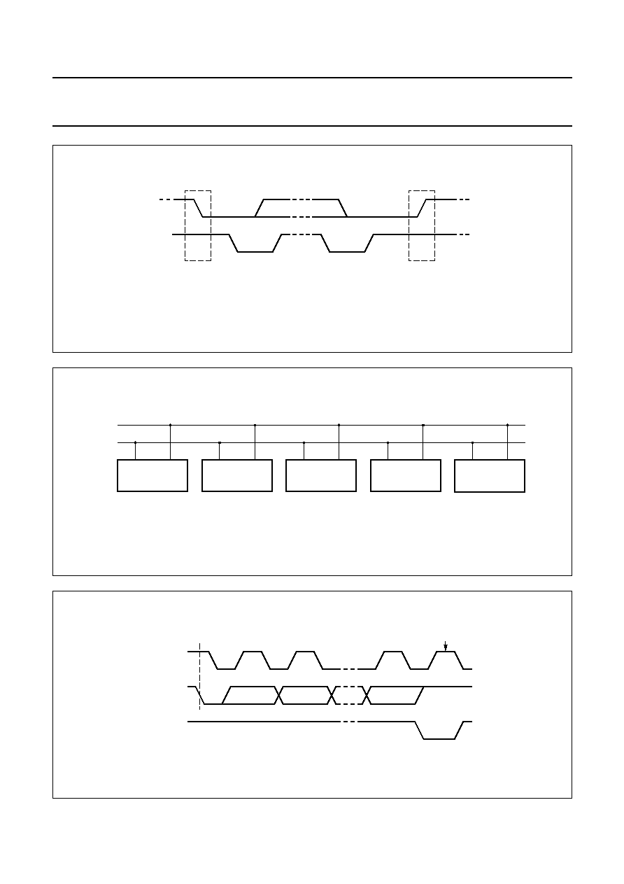
Fig.4 Direct drive mode display output waveforms.
V
on(rms)
= V
DD
-
V
SS
; V
off(rms)
= 0.
MGA737
VDD
VSS
VDD
VSS
SS
DD
V V
0
SS
DD
(V V )
BP1 Sx
Segment x
(Sx)
BP1
1
f
LCD
OFF
ON
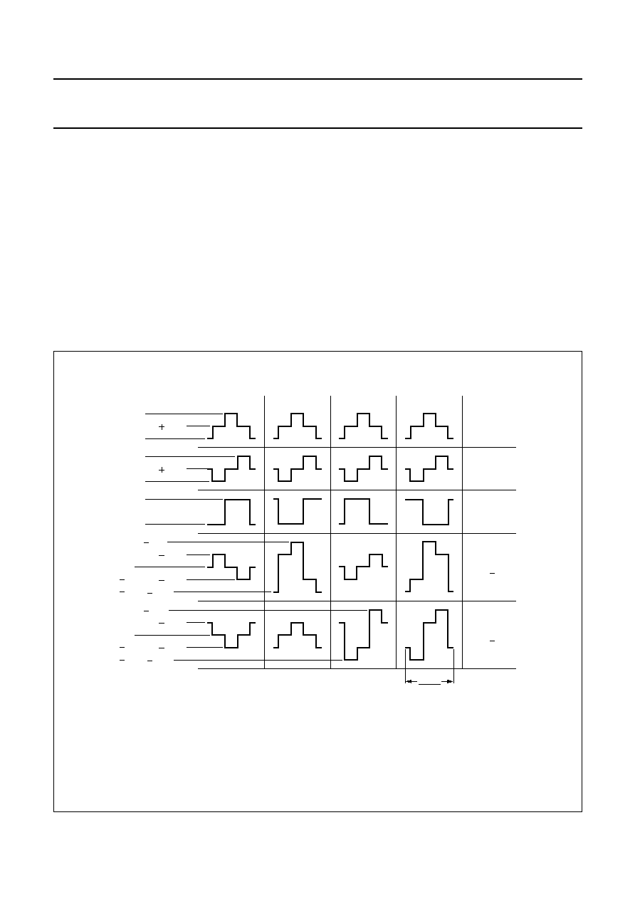
1998 Jul 30
7
Philips Semiconductors
Product specification
LCD direct/duplex driver with
I
2
C-bus interface
PCF8577C
6.5
Direct drive mode
The PCF8577C is set to the direct drive mode by loading
the MODE control bit with logic 0. In this mode only four
bytes are required to store the data for the 32 segment
drivers. Setting the BANK bit to logic 0 selects even bytes
(BANK A), setting the BANK bit to logic 1 selects odd bytes
(BANK B).
In the direct drive mode the SBV is auto-incremented by
two after the loading of each segment byte register. This
means that auto-incremented loading of BANK A or
BANK B is possible. Either bank may be completely or
partially loaded irrespective of which bank is being
displayed. Direct drive output waveforms are shown in
Fig.4.
6.6
Duplex mode
The PCF8577C is set to the duplex mode by loading the
MODE bit with logic 1. In this mode a second backplane
signal (BP2) is needed and pin A2/BP2 is used for this;
therefore A2 and its equivalent SBV bit V5 are undefined.
The SBV auto-increments by one between loaded bytes.
All of the segment bytes are required to store data for the
32 segment drivers and the BANK bit is ignored.
Duplex mode output waveforms are shown in Fig.5.
Fig.5 Duplex mode display output waveforms.
V
on(rms)
= 0.791 (V
DD
-
V
SS
); V
off(rms)
= 0.354 (V
DD
-
V
SS
).
V
on rms
(
)
V
off rms
(
)
-----------------------
2.236
=
MGA738
VDD
VSS
SS
DD
0.5 (V V )
SS
DD
0.5 (V V )
VDD
VSS
SS
DD
0.5 (V V )
VDD
VSS
SS
DD
V V
0
SS
DD
0.5 (V V )
SS
DD
(V V )
SS
DD
0.5 (V V )
SS
DD
V V
0
SS
DD
0.5 (V V )
SS
DD
(V V )
BP2 Sx
BP1 Sx
Segment x
(Sx)
BP1
BP2
1
f
LCD
OFF / OFF
ON / OFF
OFF / ON
ON / ON
1998 Jul 30
8
Philips Semiconductors
Product specification
LCD direct/duplex driver with
I
2
C-bus interface
PCF8577C
6.7
Power-on reset
At power-on reset the PCF8577C resets to a defined
starting condition as follows:
1. Both backplane outputs are set to V
SS
in master mode;
to 3-state in cascade mode
2. All segment outputs are set to V
SS
3. The segment byte registers and control register are
cleared
4. The I
2
C-bus interface is initialized.
6.8
Slave address
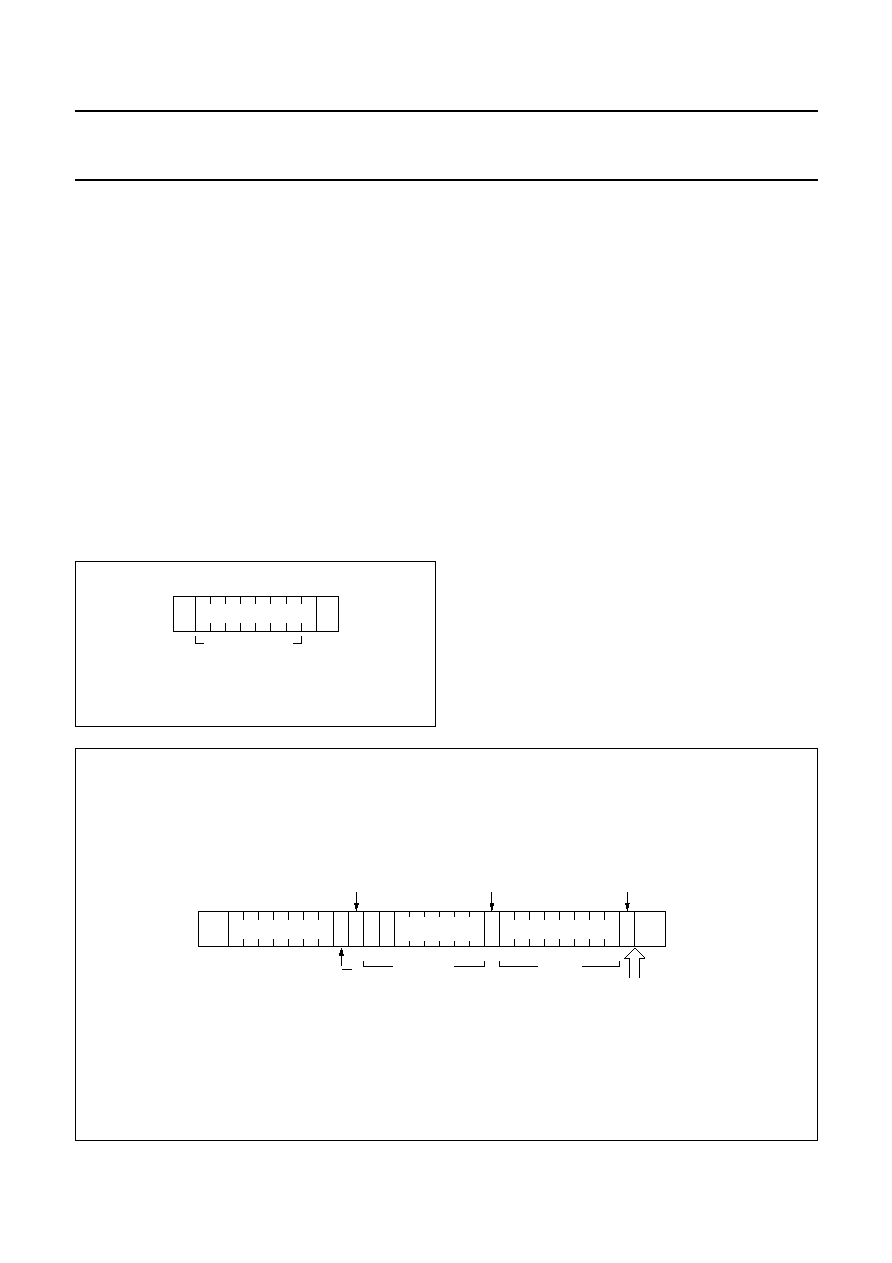
The PCF8577C slave address is shown in Fig.6.
Before any data is transmitted on the I
2
C-bus, the device
which should respond is addressed first. The addressing is
always done with the first byte transmitted after the start
procedure.
Fig.6 PCF8577C slave address.
0 1 1 1 0 1 0 0
S
A
SLAVE ADDRESS
MGA731
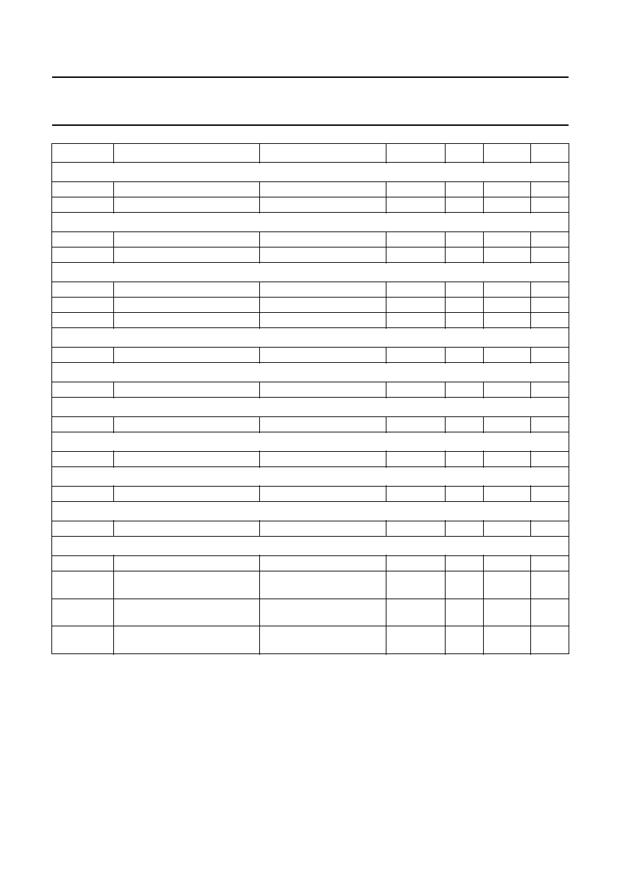
6.9
I
2
C-bus protocol
The PCF8577C I
2
C-bus protocol is shown in Fig.7.
The PCF8577C is a slave receiver and has a fixed slave
address (see Fig.6). All PCF8577Cs with the same slave
address acknowledge the slave address in parallel.
The second byte is always the control byte and is loaded
into the control register of each PCF8577C connected to
the I
2
C-bus. All addressed devices acknowledge the
control byte. Subsequent data bytes are loaded into the
segment registers of the selected device. Any number of
data bytes may be loaded in one transfer and in an
expanded system rollover of the SBV from 111 111 to
000 000 is allowed. If a stop (P) condition is given after the
control byte acknowledge the segment data will remain
unchanged. This allows the BANK bit to be toggled without
changing the segment register contents. During loading of
segment data only the selected PCF8577C gives an
acknowledge. Loading is terminated by generating a stop
(P) condition.
Fig.7 I
2
C-bus protocol.
S
A
SLAVE ADDRESS
A
A
SEGMENT DATA
P
acknowledge by
all PCF8577C
R/W
auto increment
segment byte vector
MGA732
0
MODE
BANK
SEGMENT
BYTE VECTOR
acknowledge by
all PCF8577C
acknowledge by
selected PCF8577C only
msb
lsb
n bytes
control byte
1998 Jul 30
9
Philips Semiconductors
Product specification
LCD direct/duplex driver with
I
2
C-bus interface
PCF8577C
6.10
Display memory mapping
The mapping between the eight segment registers and the segment outputs S1 to S32 is given in Tables 1 and 2.
Since only one register bit per segment is needed in the direct drive mode, the BANK bit allows swapping of display
information. If BANK is set to logic 0 even bytes (BANK A) are displayed; if BANK is set to logic 1 odd bytes (BANK B)
are displayed. BP1 is always used for the backplane output in the direct drive mode. In duplex mode even bytes
(BANK A) correspond to backplane 1 (BP1) and odd bytes (BANK B) correspond to backplane 2 (BP2).
Table 1
Segment byte-segment driver mapping in direct drive mode
Mapping example: bit 0 of register 7 controls the LCD segment S25 if BANK bit is a logic 1.
Table 2
Segment byte-segment driver mapping in duplex mode
Note
1. Where X = don't care.
Mapping example: bit 7 of register 5 controls the LCD segment S24/BP2.
MODE
BANK
V
2
V
1
V
0
SEGMENT/
BIT/
REGISTER
MSB
7
6
5
4
3
2
1
LSB
0
BACK-
PLANE
0
0
0
0
0
0
S8
S7
S6
S5
S4
S3
S2
S1
BP1
0
1
0
0
1
1
S8
S7
S6
S5
S4
S3
S2
S1
BP1
0
0
0
1
0
2
S16
S15
S14
S13
S12
S11
S10
S9
BP1
0
1
0
1
1
3
S16
S15
S14
S13
S12
S11
S10
S9
BP1
0
0
1
0
0
4
S24
S23
S22
S21
S20
S19
S18
S17
BP1
0
1
1
0
1
5
S24
S23
S22
S21
S20
S19
S18
S17
BP1
0
0
1
1
0
6
S32
S31
S30
S29
S28
S27
S26
S25
BP1
0
1
1
1
1
7
S32
S31
S30
S29
S28
S27
S26
S25
BP1
MODE
BANK
(1)
V
2
V
1
V
0
SEGMENT/
BIT/
REGISTER
MSB
7
6
5
4
3
2
1
LSB
0
BACK-
PLANE
1
X
0
0
0
0
S8
S7
S6
S5
S4
S3
S2
S1
BP1
1
X
0
0
1
1
S8
S7
S6
S5
S4
S3
S2
S1
BP2
1
X
0
1
0
2
S16
S15
S14
S13
S12
S11
S10
S9
BP1
1
X
0
1
1
3
S16
S15
S14
S13
S12
S11
S10
S9
BP2
1
X
1
0
0
4
S24
S23
S22
S21
S20
S19
S18
S17
BP1
1
X
1
0
1
5
S24
S23
S22
S21
S20
S19
S18
S17
BP2
1
X
1
1
0
6
S32
S31
S30
S29
S28
S27
S26
S25
BP1
1
X
1
1
1
7
S32
S31
S30
S29
S28
S27
S26
S25
BP2
1998 Jul 30
10
Philips Semiconductors
Product specification
LCD direct/duplex driver with
I
2
C-bus interface
PCF8577C
7
CHARACTERISTICS OF THE I
2
C-BUS
The I
2
C-bus is for 2-way, 2-line communication between
different ICs or modules. The two lines are a serial data
line (SDA) and a serial clock line (SCL). Both lines must be
connected to a positive supply via a pull-up resistor when
connected to the output stages of a device. Data transfer
may be initiated only when the I
2
C-bus is not busy.
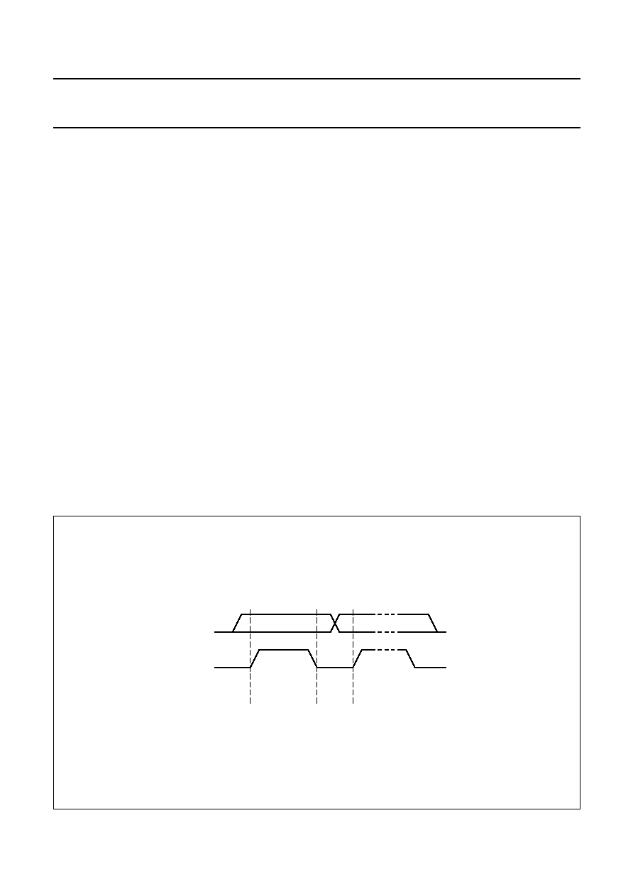
7.1
Bit transfer
One data bit is transferred during each clock pulse.
The data on the SDA line must remain stable during the
HIGH period of the clock pulse as changes in the data line
at this time will be interpreted as control signals.
7.2
Start and stop conditions
Both data and clock lines remain HIGH when the I
2
C-bus
is not busy. A HIGH-to-LOW transition of the data line,
while the clock is HIGH is defined as the start condition (S).
A LOW-to-HIGH transition of the data line while the clock
is HIGH is defined as the stop condition (P).
7.3
System configuration
A device generating a message is a `transmitter', a device
receiving a message is the `receiver'. The device that
controls the message is the `master' and the devices which
are controlled by the master are the `slaves'.
7.4
Acknowledge
The number of data bytes transferred between the start
and stop conditions from transmitter to receiver is not
limited. Each byte is followed by one acknowledge bit.
The acknowledge bit is a HIGH level put on the I
2
C-bus by
the transmitter whereas the master generates an extra
acknowledge related clock pulse. A slave receiver which is
addressed must generate an acknowledge after the
reception of each byte. Also a master must generate an
acknowledge after the reception of each byte that has
been clocked out of the slave transmitter. The device that
acknowledges has to pull down the SDA line during the
acknowledge clock pulse, set-up and hold times must be
taken into account. A master receiver must signal an end
of data to the transmitter by not generating an
acknowledge on the last byte that has been clocked out of
the slave. In this event the transmitter must leave the data
line HIGH to enable the master to generate a stop
condition.
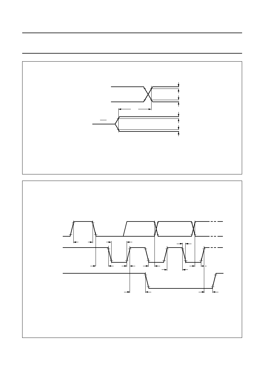
Fig.8 Bit transfer.
MBA607
data line
stable;
data valid
change
of data
allowed
SDA
SCL
1998 Jul 30
11
Philips Semiconductors
Product specification
LCD direct/duplex driver with
I
2
C-bus interface
PCF8577C
Fig.9 Definition of the start and stop conditions.
MBA608
SDA
SCL
P
STOP condition
SDA
SCL
S
START condition
Fig.10 System configuration.
MBA605
MASTER
TRANSMITTER /
RECEIVER
SLAVE
RECEIVER
SLAVE
TRANSMITTER /
RECEIVER
MASTER
TRANSMITTER
MASTER
TRANSMITTER /
RECEIVER
SDA
SCL
Fig.11 Acknowledgement on the I
2
C-bus.
handbook, full pagewidth
MBA606 - 1
START
condition
S
SCL FROM
MASTER
DATA OUTPUT
BY TRANSMITTER
DATA OUTPUT
BY RECEIVER
clock pulse for
acknowledgement
1
2
8
9
1998 Jul 30
12
Philips Semiconductors
Product specification
LCD direct/duplex driver with
I
2
C-bus interface
PCF8577C
8
LIMITING VALUES
In accordance with the Absolute Maximum Rating System (IEC 134).
Note
1. Reduce by 7.7 mW/K when T
amb
> 60
∞
C.
9
HANDLING
Inputs and outputs are protected against electrostatic discharge in normal handling. However, to be totally safe it is
desirable to take normal precautions appropriate to handling MOS devices. Advice can be found in Data Handbook IC12
under
"Handling MOS Devices".
10 DC CHARACTERISTICS
V
DD
= 2.5 to 6 V; V
SS
= 0 V; T
amb
=
-
40 to 85
∞
C; unless otherwise specified.
SYMBOL
PARAMETER
CONDITIONS
MIN.
MAX.
UNIT
V
DD
supply voltage
-
0.5
+8.0
V
V
I
input voltage on pin
-
0.5
V
DD
+ 0.5
V
I
DD
; I
SS
V
DD
or V
SS
current
-
50
+50
mA
I
I
DC input current
-
20
+20
mA
I
O
DC output current
-
25
+25
mA
P
tot
power dissipation per package
note 1
-
500
mW
P
O
power dissipation per output
-
100
mW
T
stg
storage temperature
-
65
+150
∞
C
SYMBOL
PARAMETER
CONDITIONS
MIN.
TYP.
(1)
MAX.
UNIT
Supply
V
DD
supply voltage
2.5
-
6
V
I
DD
supply current for
non-specified inputs at V
DD
or
V
SS
no load; f
SCL
= 100 kHz;
R
osc
= 1 M
;
C
osc
= 680 pF
50
125
µ
A
no load; f
SCL
= 0;
R
osc
= 1 M
;
C
osc
= 680 pF
-
25
75
µ
A
no load; f
SCL
= 0;
R
osc
= 1 M
;
C
osc
= 680 pF; V
DD
= 5 V;
T
amb
= 25
∞
C
-
25
40
µ
A
no load; f
SCL
= 0; direct
mode; A0/OSC = V
DD
;
V
DD
= 5 V; T
amb
= 25
∞
C
-
10
20
µ
A
V
POR
power-on reset level
note 2
-
1.1
2.0
V
Input A0
V
IL(A0)
LOW-level input voltage
0
-
0.05
V
V
IH(A0)
HIGH-level input voltage
V
DD
-
0.05
-
V
DD
V
1998 Jul 30
13
Philips Semiconductors
Product specification
LCD direct/duplex driver with
I
2
C-bus interface
PCF8577C
Notes
1. Typical conditions: V
DD
= 5 V; T
amb
= 25
∞
C.
2. Resets all logic when V
DD
<
V
POR
.
3. Periodically sampled, not 100% tested.
4. Outputs measured one at a time.
5. Outputs measured one at a time; V
DD
= 5 V; I
load
= 100
µ
A.
Input A1
V
IL(A1)
LOW-level input voltage
0
-
0.3V
DD
V
V
IH(A1)
HIGH-level input voltage
0.7V
DD
-
V
DD
V
Input A2
V
IL(A2)
LOW-level input voltage
0
-
0.10
V
V
IH(A2)
HIGH-level input voltage
V
DD
-
0.10
-
V
DD
V
Input SCL; SDA
V
IL(SCL; SDA)
LOW-level input voltage
0
-
0.3V
DD
V
V
IH(SCL; SDA)
HIGH-level input voltage
0.7V
DD
-
6
V
C
i
input capacitance
note 3
-
-
7
pF
Output SDA
I
OL
LOW-level output current
V
OL
= 0.4 V; V
DD
= 5 V
3
-
-
mA
A1; SCL; SDA
I
L1
leakage current
V
I
= V
DD
or V
SS
-
1
-
+1
µ
A
A2/BP2; BP1
I
L2
leakage current
V
I
= V
DD
or V
SS
-
5
-
+5
µ
A
A2/BP2
I
pd
pull-down current
V
I
= V
DD
-
5
-
1.5
-
µ
A
A0/OSC
I
L3
leakage current
V
I
= V
DD
-
1
-
-
µ
A
Oscillator
I
OSC
start-up current
V
I
= V
SS
-
1.2
5
µ
A
LCD outputs
V
DC
DC component of LCD driver
-
±
20
-
mV
I
OL1
LOW-level segment output
current
V
DD
= 5 V; V
OL
= 0.8 V;
note 4
0.3
-
-
mA
I
OH1
HIGH-level segment output
current
V
DD
= 5 V;
V
OH
= V
DD
-
0.8 V; note 4
-
-
-
0.3
mA
R
BP
backplane output resistance
(BP1; BP2)
V
O
= V
SS
or V
DD
or
1
/
2
(V
SS
+ V
DD
); note 5
-
0.4
5
k
SYMBOL
PARAMETER
CONDITIONS
MIN.
TYP.
(1)
MAX.
UNIT
1998 Jul 30
14
Philips Semiconductors
Product specification
LCD direct/duplex driver with
I
2
C-bus interface
PCF8577C
11 AC CHARACTERISTICS
V
DD
= 2.5 to 6 V; T
amb
=
-
40 to 85
∞
C; unless otherwise specified. All the timing values are valid within the operating
supply voltage and ambient temperature range and refer to V
IL
and V
IH
with an input voltage swing of V
SS
to V
DD
.
Note
1. Typical conditions: V
DD
= 5 V; T
amb
= 25
∞
C.
SYMBOL
PARAMETER
CONDITIONS
MIN.
TYP.
(1)
MAX.
UNIT
f
LCD
display frequency
C
osc
= 680 pF; R
osc
= 1 M
65
90
120
Hz
t
BS
driver delays with test loads
V
DD
= 5 V
-
20
100
µ
s
I
2
C-bus
f
SCL
SCL clock frequency
-
-
100
kHz
t
SW
tolerable spike width on I
2
C-bus T
amb
= 25
∞
C
-
-
100
ns
t
BUF
I
2
C-bus free time
4.7
-
-
µ
s
t
SU;STA
START condition set-up time
4.0
-
-
µ
s
t
HD;STA
START condition hold time
4.0
-
-
µ
s
t
LOW
SCL LOW time
4.7
-
-
µ
s
t
HIGH
SCL HIGH time
4.0
-
-
µ
s
t
r
SCL and SDA rise time
-
-
1.0
µ
s
t
f
SCL and SDA fall time
-
-
0.3
µ
s
t
SU;DAT
data set-up time
250
-
-
ns
t
HD;DAT
data hold time
0
-
-
ns
t
SU;STO
STOP condition set-up time
4.0
-
-
µ
s
Fig.12 Test loads.
MGA730
1.5 k
6.8 k
VDD
(V V ) / 2
DD
SS
S32 to S1
(pins 1 to 32)
SCL, SDA
(pins 39, 40)
1998 Jul 30
15
Philips Semiconductors
Product specification
LCD direct/duplex driver with
I
2
C-bus interface
PCF8577C
Fig.13 Driver timing waveforms.
MGA729
BP1, BP2
(V = 5 V)
DD
0.5 V
BS
t
Sx
VDD
2
0.5 V
0.5 V
0.5 V
(V = 5 V)
DD
Fig.14 I
2
C-bus timing diagram; rise and fall times refer to V
IL
and V
IH
.
handbook, full pagewidth
SDA
MGA728
SDA
SCL
t SU;STA
t
SU;STO
t
HD;STA
t BUF
t LOW
t HD;DAT
t HIGH
t r
t f
t SU;DAT
1998
Jul
30
16
Philips Semiconductors
Product specification
LCD direct/duplex driver with
I
2
C-bus interface
PCF8577C
This text is here in white to force landscape pages to be rotated correctly when browsing through the pdf in the Acrobat reader.This text is here in
_
white to force landscape pages to be rotated correctly when browsing through the pdf in the Acrobat reader.This text is here inThis text is here in
white to force landscape pages to be rotated correctly when browsing through the pdf in the Acrobat reader. white to force landscape pages to be ...
12
APPLICA
TION INFORMA
TION
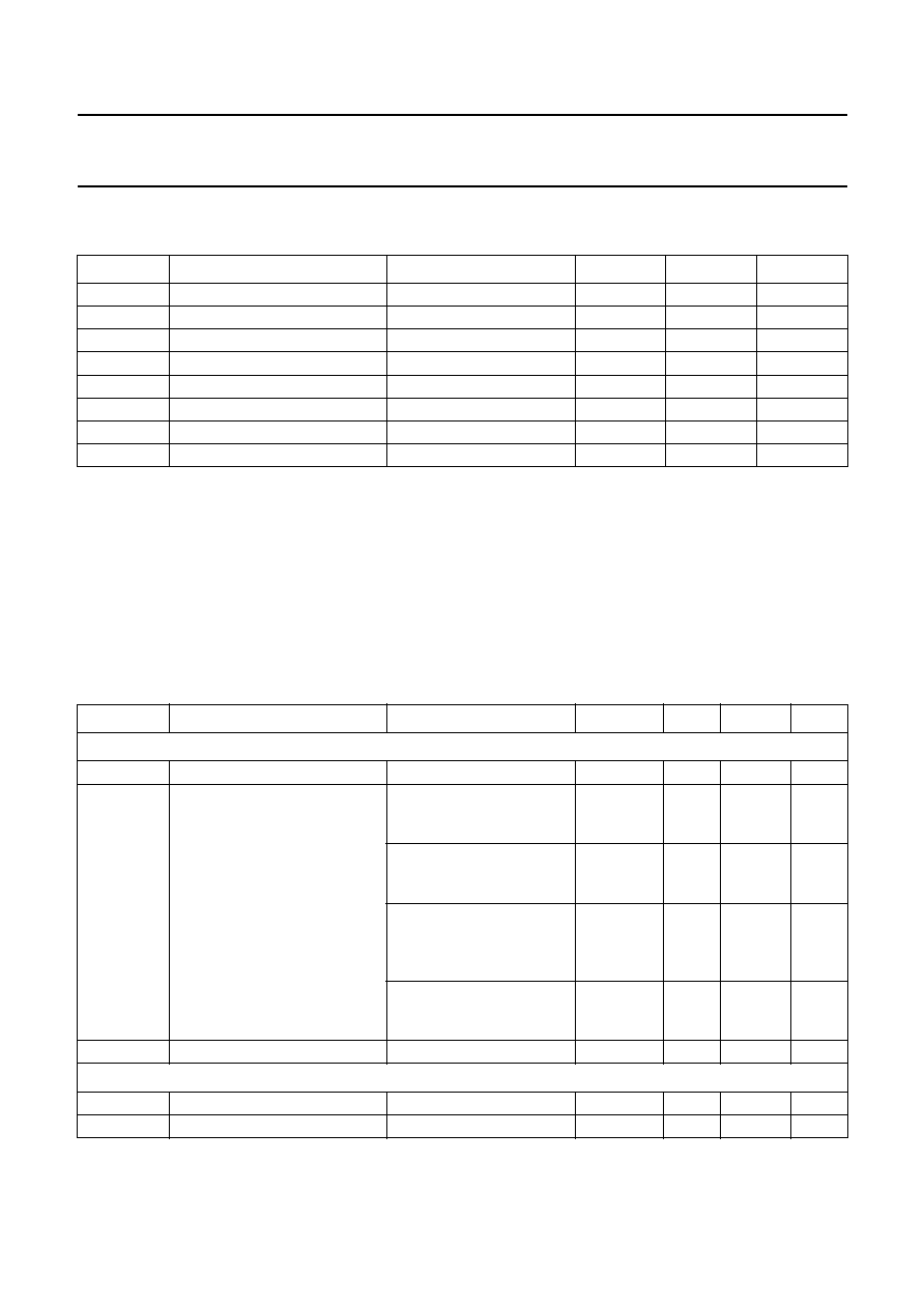
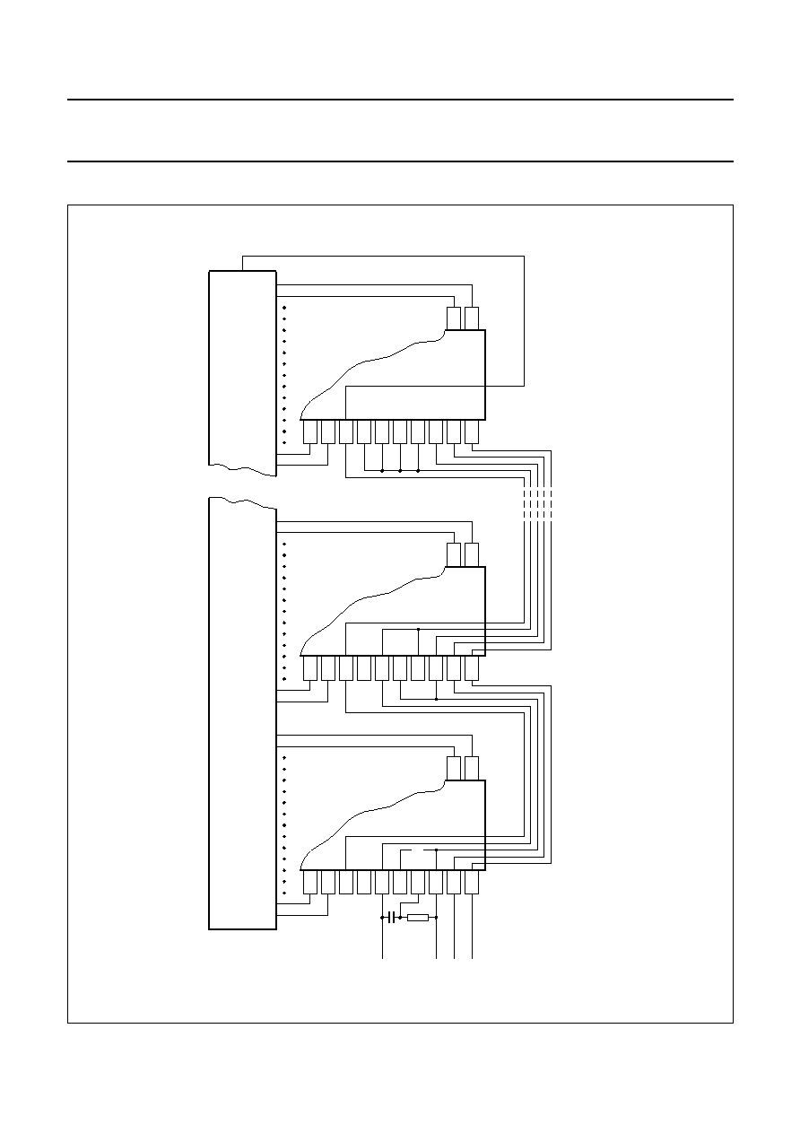
Fig.15 Direct display driver; expansion to 256 segments using eight PCF8577Cs.
MGA735
VDD
VSS
SDA
SCL
A0
A1
BP2
BP1
S32
S31
S1
S2
PCF8577C
OSC
A2
Cosc
Rosc
VDD
VSS
SDA
SCL
device subaddress
A2.A1.A0 = 000
VDD
VSS
SDA
SCL
A0
A1
BP2
BP1
S32
S31
S1
S2
PCF8577C
OSC
A2
device subaddress
A2.A1.A0 = 001
VDD
VSS
SDA
SCL
A0
A1
BP2
BP1
S32
S31
S1
S2
PCF8577C
OSC
A2
device subaddress
A2.A1.A0 = 111
256
64
33
32
1
backplane
DIRECT DRIVE LCD DISPLAY
1998
Jul
30
17
Philips Semiconductors
Product specification
LCD direct/duplex driver with
I
2
C-bus interface
PCF8577C
This text is here in white to force landscape pages to be rotated correctly when browsing through the pdf in the Acrobat reader.This text is here in
_
white to force landscape pages to be rotated correctly when browsing through the pdf in the Acrobat reader.This text is here inThis text is here in
white to force landscape pages to be rotated correctly when browsing through the pdf in the Acrobat reader. white to force landscape pages to be ...
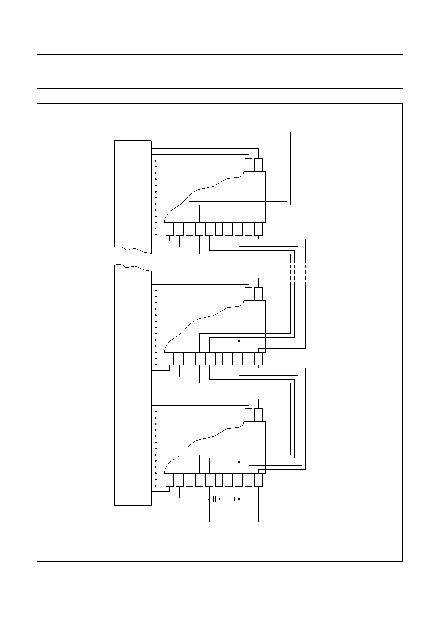
Fig.16 Duplex display; expansion to 2
◊
128 segments using four PCF8577Cs.
MGA736
VDD
VSS
SDA
SCL
A0
A1
BP2
BP1
S32
S31
S1
S2
PCF8577C
OSC
A2
Cosc
R
osc
VDD
VSS
SDA
SCL
device subaddress
A1.A0 = 00
VDD
VSS
SDA
SCL
A0
A1
BP2
BP1
S32
S31
S1
S2
PCF8577C
OSC
A2
device subaddress
A1.A0 = 01
VDD
VSS
SDA
SCL
A0
A1
BP2
BP1
S32
S31
S1
S2
PCF8577C
OSC
A2
device subaddress
A1.A0 = 11
128
64
33
32
1
DUPLEX LCD DISPLAY
BP2
BP1
1998 Jul 30
18
Philips Semiconductors
Product specification
LCD direct/duplex driver with
I
2
C-bus interface
PCF8577C
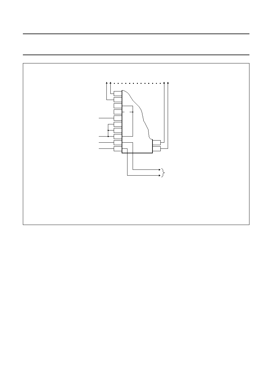
Fig.17 Use of PCF8577C as a 32-bit output expander in I
2
C-bus application.
MODE bit must always be set to logic 0 (direct drive).
BANK switching is permitted.
BP1 must always be connected to V
SS
and A0/OSC must be connected to either V
DD
or V
SS
(no LCD modulation).
MGA734
VDD
VSS
SDA
SCL
A0
A1
BP2
BP1
S32
S31
S1
S2
PCF8577C
OSC
A2
VDD
VSS
SDA
SCL
device subaddress
A2, A1, A0 = 000
expansion
32 output lines
1998 Jul 30
19
Philips Semiconductors
Product specification
LCD direct/duplex driver with
I
2
C-bus interface
PCF8577C
13 CHIP DIMENSIONS AND BONDING PAD LOCATIONS
Fig.18 Bonding pad locations.
Chip area = 4.62 mm
2
.
Thickness = 381
±
25
µ
m.
n-substrate (back) connected to V
DD
.
Bonding pad dimensions = 110
µ
m
◊
110
µ
m.
handbook, full pagewidth
MGA726
VDD
A2/BP2
BP1
V
SS
SDA
SCL
A0/OSC
A1
S32
S31
S30
S29
S28
S27
S26
S25
S24
S23
S22
S21
S20
S19
S18
S1
S2
S3
S4
S5
S6
S7
23
22
21
20
19
18
17
16
15
14
13
12
11
10
9
8
7
6
5
4
3
2
1
40
39
38
37
36
35
34
33
32
31
30
29
28
27
26
24
25
S17
S16
S15
S14
S13
S8
S9
S10
S1
1
S12
2.31
mm
2 mm
PCF8577C
x
y
0
0
handbook, halfpage
MBE924
Fig.19 Reference marks.
1998 Jul 30
20
Philips Semiconductors
Product specification
LCD direct/duplex driver with
I
2
C-bus interface
PCF8577C
Table 3
Bonding pad locations (dimensions in
µ
m)
All x and y co-ordinates are referenced to the centre of the chip, see Fig.18.
SIGNAL
PAD POSITION CENTRED
x
y
S32
-
86
941
S31
-
257
941
S30
-
428
941
S29
-
599
941
S28
-
836
941
S27
-
836
769
S26
-
836
598
S25
-
836
427
S24
-
836
256
S23
-
836
85
S22
-
836
-
86
S21
-
836
-
257
S20
-
836
-
428
S19
-
836
-
599
S18
-
836
-
770
S17
-
836
-
941
S16
-
599
-
941
S15
-
428
-
941
S14
-
257
-
941
S13
-
86
-
941
S12
85
-
941
S11
256
-
941
S10
427
-
941
S9
598
-
941
S8
836
-
941
S7
836
-
770
S6
836
-
599
S5
836
-
428
S4
836
-
257
S3
836
-
86
S2
836
85
S1
836
256
BP1
836
427
A2/BP2
836
598
V
DD
836
769
A1
836
941
A0/OSC
598
941
V
SS
427
941
SCL
256
941
SDA
85
941
Recpats
C
-
586
-
699
F
-
580
663
SIGNAL
PAD POSITION CENTRED
x
y
1998 Jul 30
21
Philips Semiconductors
Product specification
LCD direct/duplex driver with
I
2
C-bus interface
PCF8577C
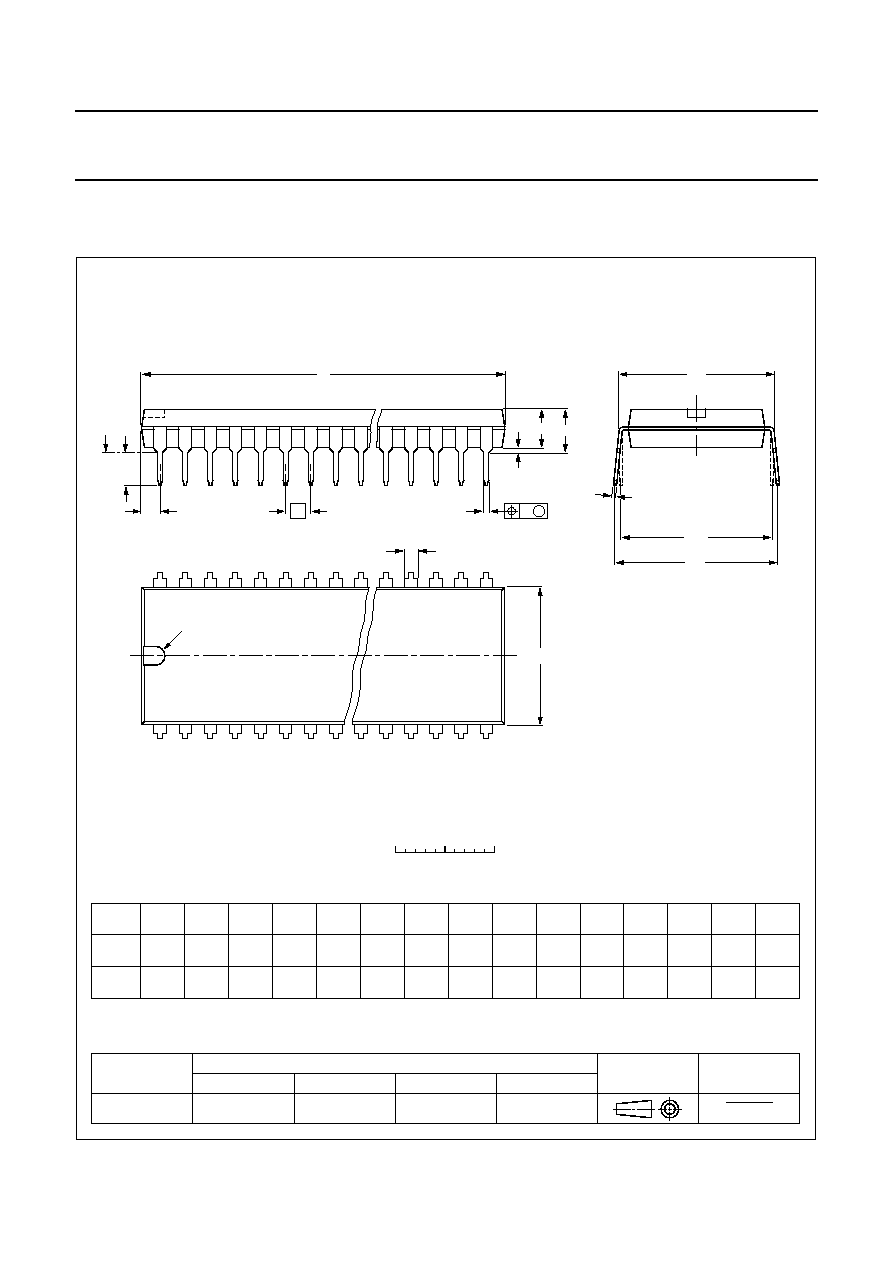
14 PACKAGE OUTLINES
UNIT
A
max.
1
2
b
1
c
D
E
e
M
H
L
REFERENCES
OUTLINE
VERSION
EUROPEAN
PROJECTION
ISSUE DATE
IEC
JEDEC
EIAJ
mm
inches
DIMENSIONS (inch dimensions are derived from the original mm dimensions)
SOT129-1
92-11-17
95-01-14
A
min.
A
max.
b
Z
max.
w
M
E
e
1
1.70
1.14
0.53
0.38
0.36
0.23
52.50
51.50
14.1
13.7
3.60
3.05
0.254
2.54
15.24
15.80
15.24
17.42
15.90
2.25
4.7
0.51
4.0
0.067
0.045
0.021
0.015
0.014
0.009
2.067
2.028
0.56
0.54
0.14
0.12
0.01
0.10
0.60
0.62
0.60
0.69
0.63
0.089
0.19
0.020
0.16
051G08
MO-015AJ
M
H
c
(e )
1
M
E
A
L
seating plane
A
1
w
M
b
1
e
D
A
2
Z
40
1
21
20
b
E
pin 1 index
0
5
10 mm
scale
Note
1. Plastic or metal protrusions of 0.25 mm maximum per side are not included.
(1)
(1)
(1)
DIP40: plastic dual in-line package; 40 leads (600 mil)
SOT129-1
1998 Jul 30
22
Philips Semiconductors
Product specification
LCD direct/duplex driver with
I
2
C-bus interface
PCF8577C
UNIT
A
1
A
2
A
3
b
p
c
D
(1)
E
(2)
Z
(1)
e
H
E
L
L
p
Q
y
w
v
REFERENCES
OUTLINE
VERSION
EUROPEAN
PROJECTION
ISSUE DATE
IEC
JEDEC
EIAJ
mm
inches
0.3
0.1
2.45
2.25
0.25
0.42
0.30
0.22
0.14
15.6
15.2
7.6
7.5
0.762
2.25
12.3
11.8
1.15
1.05
0.6
0.3
7
0
o
o
0.1
0.1
DIMENSIONS (inch dimensions are derived from the original mm dimensions)
Notes
1. Plastic or metal protrusions of 0.4 mm maximum per side are not included.
2. Plastic interlead protrusions of 0.25 mm maximum per side are not included.
1.7
1.5
SOT158-1
92-11-17
95-01-24
X
w
M
A
A
1
A
2
b
p
D
H
E
L
p
Q
detail X
E
Z
e
c
L
v
M
A
(A )
3
A
y
40
20
21
1
pin 1 index
0.012
0.004
0.096
0.089
0.017
0.012
0.0087
0.0055
0.61
0.60
0.30
0.29
0.03
0.089
0.48
0.46
0.045
0.041
0.024
0.012
0.004
0.2
0.008
0.004
0.067
0.059
0.010
0
5
10 mm
scale
VSO40: plastic very small outline package; 40 leads
SOT158-1
A
max.
2.70
0.11

1998 Jul 30
23
Philips Semiconductors
Product specification
LCD direct/duplex driver with
I
2
C-bus interface
PCF8577C
15 SOLDERING
15.1
Introduction
There is no soldering method that is ideal for all IC
packages. Wave soldering is often preferred when
through-hole and surface mounted components are mixed
on one printed-circuit board. However, wave soldering is
not always suitable for surface mounted ICs, or for
printed-circuits with high population densities. In these
situations reflow soldering is often used.
This text gives a very brief insight to a complex technology.
A more in-depth account of soldering ICs can be found in
our
"Data Handbook IC26; Integrated Circuit Packages"
(order code 9398 652 90011).
15.2
DIP
15.2.1
S
OLDERING BY DIPPING OR BY WAVE
The maximum permissible temperature of the solder is
260
∞
C; solder at this temperature must not be in contact
with the joint for more than 5 seconds. The total contact
time of successive solder waves must not exceed
5 seconds.
The device may be mounted up to the seating plane, but
the temperature of the plastic body must not exceed the
specified maximum storage temperature (T
stg max
). If the
printed-circuit board has been pre-heated, forced cooling
may be necessary immediately after soldering to keep the
temperature within the permissible limit.
15.2.2
R
EPAIRING SOLDERED JOINTS
Apply a low voltage soldering iron (less than 24 V) to the
lead(s) of the package, below the seating plane or not
more than 2 mm above it. If the temperature of the
soldering iron bit is less than 300
∞
C it may remain in
contact for up to 10 seconds. If the bit temperature is
between 300 and 400
∞
C, contact may be up to 5 seconds.
15.3
VSO
15.3.1
R
EFLOW SOLDERING
Reflow soldering techniques are suitable for all VSO
packages.
Reflow soldering requires solder paste (a suspension of
fine solder particles, flux and binding agent) to be applied
to the printed-circuit board by screen printing, stencilling or
pressure-syringe dispensing before package placement.
Several techniques exist for reflowing; for example,
thermal conduction by heated belt. Dwell times vary
between 50 and 300 seconds depending on heating
method. Typical reflow temperatures range from
215 to 250
∞
C.
Preheating is necessary to dry the paste and evaporate
the binding agent. Preheating duration: 45 minutes at
45
∞
C.
15.3.2
W
AVE SOLDERING
Wave soldering techniques can be used for all VSO
packages if the following conditions are observed:
∑
A double-wave (a turbulent wave with high upward
pressure followed by a smooth laminar wave) soldering
technique should be used.
∑
The longitudinal axis of the package footprint must be
parallel to the solder flow.
∑
The package footprint must incorporate solder thieves at
the downstream end.
During placement and before soldering, the package must
be fixed with a droplet of adhesive. The adhesive can be
applied by screen printing, pin transfer or syringe
dispensing. The package can be soldered after the
adhesive is cured.
Maximum permissible solder temperature is 260
∞
C, and
maximum duration of package immersion in solder is
10 seconds, if cooled to less than 150
∞
C within
6 seconds. Typical dwell time is 4 seconds at 250
∞
C.
A mildly-activated flux will eliminate the need for removal
of corrosive residues in most applications.
15.3.3
R
EPAIRING SOLDERED JOINTS
Fix the component by first soldering two diagonally-
opposite end leads. Use only a low voltage soldering iron
(less than 24 V) applied to the flat part of the lead. Contact
time must be limited to 10 seconds at up to 300
∞
C. When
using a dedicated tool, all other leads can be soldered in
one operation within 2 to 5 seconds between
270 and 320
∞
C.
1998 Jul 30
24
Philips Semiconductors
Product specification
LCD direct/duplex driver with
I
2
C-bus interface
PCF8577C
16 DEFINITIONS
17 LIFE SUPPORT APPLICATIONS
These products are not designed for use in life support appliances, devices, or systems where malfunction of these
products can reasonably be expected to result in personal injury. Philips customers using or selling these products for
use in such applications do so at their own risk and agree to fully indemnify Philips for any damages resulting from such
improper use or sale.
18 PURCHASE OF PHILIPS I
2
C COMPONENTS
Data sheet status
Objective specification
This data sheet contains target or goal specifications for product development.
Preliminary specification
This data sheet contains preliminary data; supplementary data may be published later.
Product specification
This data sheet contains final product specifications.
Limiting values
Limiting values given are in accordance with the Absolute Maximum Rating System (IEC 134). Stress above one or
more of the limiting values may cause permanent damage to the device. These are stress ratings only and operation
of the device at these or at any other conditions above those given in the Characteristics sections of the specification
is not implied. Exposure to limiting values for extended periods may affect device reliability.
Application information
Where application information is given, it is advisory and does not form part of the specification.
Purchase of Philips I
2
C components conveys a license under the Philips' I
2
C patent to use the
components in the I
2
C system provided the system conforms to the I
2
C specification defined by
Philips. This specification can be ordered using the code 9398 393 40011.

1998 Jul 30
25
Philips Semiconductors
Product specification
LCD direct/duplex driver with
I
2
C-bus interface
PCF8577C
NOTES

1998 Jul 30
26
Philips Semiconductors
Product specification
LCD direct/duplex driver with
I
2
C-bus interface
PCF8577C
NOTES

1998 Jul 30
27
Philips Semiconductors
Product specification
LCD direct/duplex driver with
I
2
C-bus interface
PCF8577C
NOTES

Internet: http://www.semiconductors.philips.com
Philips Semiconductors ≠ a worldwide company
© Philips Electronics N.V. 1998
SCA60
All rights are reserved. Reproduction in whole or in part is prohibited without the prior written consent of the copyright owner.
The information presented in this document does not form part of any quotation or contract, is believed to be accurate and reliable and may be changed
without notice. No liability will be accepted by the publisher for any consequence of its use. Publication thereof does not convey nor imply any license
under patent- or other industrial or intellectual property rights.
Middle East: see Italy
Netherlands: Postbus 90050, 5600 PB EINDHOVEN, Bldg. VB,
Tel. +31 40 27 82785, Fax. +31 40 27 88399
New Zealand: 2 Wagener Place, C.P.O. Box 1041, AUCKLAND,
Tel. +64 9 849 4160, Fax. +64 9 849 7811
Norway: Box 1, Manglerud 0612, OSLO,
Tel. +47 22 74 8000, Fax. +47 22 74 8341
Pakistan: see Singapore
Philippines: Philips Semiconductors Philippines Inc.,
106 Valero St. Salcedo Village, P.O. Box 2108 MCC, MAKATI,
Metro MANILA, Tel. +63 2 816 6380, Fax. +63 2 817 3474
Poland: Ul. Lukiska 10, PL 04-123 WARSZAWA,
Tel. +48 22 612 2831, Fax. +48 22 612 2327
Portugal: see Spain
Romania: see Italy
Russia: Philips Russia, Ul. Usatcheva 35A, 119048 MOSCOW,
Tel. +7 095 755 6918, Fax. +7 095 755 6919
Singapore: Lorong 1, Toa Payoh, SINGAPORE 319762,
Tel. +65 350 2538, Fax. +65 251 6500
Slovakia: see Austria
Slovenia: see Italy
South Africa: S.A. PHILIPS Pty Ltd., 195-215 Main Road Martindale,
2092 JOHANNESBURG, P.O. Box 7430 Johannesburg 2000,
Tel. +27 11 470 5911, Fax. +27 11 470 5494
South America: Al. Vicente Pinzon, 173, 6th floor,
04547-130 S√O PAULO, SP, Brazil,
Tel. +55 11 821 2333, Fax. +55 11 821 2382
Spain: Balmes 22, 08007 BARCELONA,
Tel. +34 93 301 6312, Fax. +34 93 301 4107
Sweden: Kottbygatan 7, Akalla, S-16485 STOCKHOLM,
Tel. +46 8 5985 2000, Fax. +46 8 5985 2745
Switzerland: Allmendstrasse 140, CH-8027 ZÐRICH,
Tel. +41 1 488 2741 Fax. +41 1 488 3263
Taiwan: Philips Semiconductors, 6F, No. 96, Chien Kuo N. Rd., Sec. 1,
TAIPEI, Taiwan Tel. +886 2 2134 2865, Fax. +886 2 2134 2874
Thailand: PHILIPS ELECTRONICS (THAILAND) Ltd.,
209/2 Sanpavuth-Bangna Road Prakanong, BANGKOK 10260,
Tel. +66 2 745 4090, Fax. +66 2 398 0793
Turkey: Talatpasa Cad. No. 5, 80640 GÐLTEPE/ISTANBUL,
Tel. +90 212 279 2770, Fax. +90 212 282 6707
Ukraine: PHILIPS UKRAINE, 4 Patrice Lumumba str., Building B, Floor 7,
252042 KIEV, Tel. +380 44 264 2776, Fax. +380 44 268 0461
United Kingdom: Philips Semiconductors Ltd., 276 Bath Road, Hayes,
MIDDLESEX UB3 5BX, Tel. +44 181 730 5000, Fax. +44 181 754 8421
United States: 811 East Arques Avenue, SUNNYVALE, CA 94088-3409,
Tel. +1 800 234 7381
Uruguay: see South America
Vietnam: see Singapore
Yugoslavia: PHILIPS, Trg N. Pasica 5/v, 11000 BEOGRAD,
Tel. +381 11 625 344, Fax.+381 11 635 777
For all other countries apply to: Philips Semiconductors,
International Marketing & Sales Communications, Building BE-p, P.O. Box 218,
5600 MD EINDHOVEN, The Netherlands, Fax. +31 40 27 24825
Argentina: see South America
Australia: 34 Waterloo Road, NORTH RYDE, NSW 2113,
Tel. +61 2 9805 4455, Fax. +61 2 9805 4466
Austria: Computerstr. 6, A-1101 WIEN, P.O. Box 213, Tel. +43 160 1010,
Fax. +43 160 101 1210
Belarus: Hotel Minsk Business Center, Bld. 3, r. 1211, Volodarski Str. 6,
220050 MINSK, Tel. +375 172 200 733, Fax. +375 172 200 773
Belgium: see The Netherlands
Brazil: see South America
Bulgaria: Philips Bulgaria Ltd., Energoproject, 15th floor,
51 James Bourchier Blvd., 1407 SOFIA,
Tel. +359 2 689 211, Fax. +359 2 689 102
Canada: PHILIPS SEMICONDUCTORS/COMPONENTS,
Tel. +1 800 234 7381
China/Hong Kong: 501 Hong Kong Industrial Technology Centre,
72 Tat Chee Avenue, Kowloon Tong, HONG KONG,
Tel. +852 2319 7888, Fax. +852 2319 7700
Colombia: see South America
Czech Republic: see Austria
Denmark: Prags Boulevard 80, PB 1919, DK-2300 COPENHAGEN S,
Tel. +45 32 88 2636, Fax. +45 31 57 0044
Finland: Sinikalliontie 3, FIN-02630 ESPOO,
Tel. +358 9 615800, Fax. +358 9 61580920
France: 51 Rue Carnot, BP317, 92156 SURESNES Cedex,
Tel. +33 1 40 99 6161, Fax. +33 1 40 99 6427
Germany: Hammerbrookstraþe 69, D-20097 HAMBURG,
Tel. +49 40 23 53 60, Fax. +49 40 23 536 300
Greece: No. 15, 25th March Street, GR 17778 TAVROS/ATHENS,
Tel. +30 1 4894 339/239, Fax. +30 1 4814 240
Hungary: see Austria
India: Philips INDIA Ltd, Band Box Building, 2nd floor,
254-D, Dr. Annie Besant Road, Worli, MUMBAI 400 025,
Tel. +91 22 493 8541, Fax. +91 22 493 0966
Indonesia: PT Philips Development Corporation, Semiconductors Division,
Gedung Philips, Jl. Buncit Raya Kav.99-100, JAKARTA 12510,
Tel. +62 21 794 0040 ext. 2501, Fax. +62 21 794 0080
Ireland: Newstead, Clonskeagh, DUBLIN 14,
Tel. +353 1 7640 000, Fax. +353 1 7640 200
Israel: RAPAC Electronics, 7 Kehilat Saloniki St, PO Box 18053,
TEL AVIV 61180, Tel. +972 3 645 0444, Fax. +972 3 649 1007
Italy: PHILIPS SEMICONDUCTORS, Piazza IV Novembre 3,
20124 MILANO, Tel. +39 2 6752 2531, Fax. +39 2 6752 2557
Japan: Philips Bldg 13-37, Kohnan 2-chome, Minato-ku,
TOKYO 108-8507, Tel. +81 3 3740 5130, Fax. +81 3 3740 5077
Korea: Philips House, 260-199 Itaewon-dong, Yongsan-ku, SEOUL,
Tel. +82 2 709 1412, Fax. +82 2 709 1415
Malaysia: No. 76 Jalan Universiti, 46200 PETALING JAYA, SELANGOR,
Tel. +60 3 750 5214, Fax. +60 3 757 4880
Mexico: 5900 Gateway East, Suite 200, EL PASO, TEXAS 79905,
Tel. +9-5 800 234 7381
Printed in The Netherlands
415106/1200/04/pp28
Date of release: 1998 Jul 30
Document order number:
9397 750 04197