
Philips Semiconductors
Product specification
87L51FA/87L51FB
CMOS single-chip 3.0V 8-bit microcontrollers
3-150
1996 Aug 16
853-1729 17200
DESCRIPTION
The 87L51FA and 87L51FB Single-Chip 3.0V 8-Bit Microcontrollers
are manufactured in an advanced CMOS process and are
derivatives of the 80C51 microcontroller family. The 87L51FA/B has
the same instruction set as the 80C51.
This device provides architectural enhancements that make it
applicable in a variety of applications for general control systems.
The 87L51FA contains 8k
◊
8 memory and the 87L51FB contains
16K
◊
8 memory, a volatile 256
◊
8 read/write data memory, four
8-bit I/O ports, three 16-bit timer/event counters, a Programmable
Counter Array (PCA), a multi-source, two-priority-level, nested
interrupt structure, an enhanced UART and on-chip oscillator and
timing circuits. For systems that require extra capability, the
87L51FA/B can be expanded using standard 3.3V TTL compatible
memories and logic.
Its added features make it an even more powerful microcontroller for
applications that require pulse width modulation, high-speed I/O and
up/down counting capabilities such as motor control. It also has a
more versatile serial channel that facilitates multiprocessor
communications.
FEATURES
∑
80C51 central processing unit
∑
3.0 to 4.5V V
CC
range
∑
8k
◊
8 EPROM (87L51FA)
16k
◊
8 EPROM (87L51FB)
≠ Expandable externally to 64k bytes
≠ Quick Pulse programming algorithm
≠ Two level program security system
∑
256
◊
8 RAM, expandable externally to 64k bytes
∑
Three 16-bit timer/counters
≠ T2 is an up/down counter
∑
Programmable Counter Array (PCA)
≠ High speed output
≠ Capture/compare
≠ Pulse Width Modulator
≠ Watchdog Timer
∑
Four 8-bit I/O ports
∑
Full-duplex enhanced UART
≠ Framing error detection
≠ Automatic address recognition
∑
Power control modes
≠ Idle mode
≠ Power-down mode
∑
Once (On Circuit Emulation) Mode
∑
Five package styles
∑
OTP package available
PIN CONFIGURATIONS
1
2
3
4
5
6
7
8
9
10
11
12
13
14
15
16
17
18
19
20
21
22
23
24
25
26
27
28
29
30
31
32
33
34
35
36
37
38
39
40
T2/P1.0
T2EX/P1.1
ECI/P1.2
CEX0/P1.3
CEX1/P1.4
CEX2/P1.5
CEX3/P1.6
RST
RxD/P3.0
TxD/P3.1
INT0/P3.2
INT1/P3.3
T0/P3.4
T1/P3.5
CEX4/P1.7
WR/P3.6
RD/P3.7
XTAL2
XTAL1
V
SS
P2.0/A8
P2.1/A9
P2.2/A10
P2.3/A11
P2.4/A12
P2.5/A13
P2.6/A14
P2.7/A15
PSEN
ALE/PROG
EA/V
PP
P0.7/AD7
P0.6/AD6
P0.5/AD5
P0.4/AD4
P0.3/AD3
P0.2/AD2
P0.1/AD1
P0.0/AD0
V
CC
DUAL
IN-LINE
PACKAGE
SU00021

Philips Semiconductors
Product specification
87L51FA/87L51FB
CMOS single-chip 3.0V 8-bit microcontrollers
1996 Aug 16
3-151
ORDERING INFORMATION
8k
◊
8
ROM
1
6k
◊
8
ROM
1
8k
◊
8
EPROM
2
16k
◊
8
EPROM
2
TEMPERATURE RANGE
∞
C
AND PACKAGE
FREQ.
(MHz)
DWG.
#
S83L51FA≠4N40
S83L51FB≠4N40
S87L51FA≠4N40
S87L51FB≠4N40
OTP
0 to +70,
40-Pin Plastic Dual In-line Package
3.5
to
16
SOT129-1
S87L51FA≠4F40
S87L51FB≠4F40
UV
0 to +70,
40-Pin Ceramic Dual In-line Package
w/Window
3.5
to
16
0590B
S83L51FA≠4A44
S83L51FB≠4A44
S87L51FA≠4A44
S87L51FB≠4A44
OTP
0 to +70,
44-Pin Plastic Leaded Chip Carrier
3.5
to
16
SOT187-2
S87L51FA≠4K44
S87L51FB≠4K44
UV
0 to +70,
44-Pin Ceramic Leaded Chip Carrier
w/Window
3.5
to
16
1472A
S83L51FA≠4B44
S83L51FB≠4B44
S87L51FA≠4B44
S87L51FB≠4B44
OTP
0 to +70,
44-Pin Plastic Quad Flat Pack
3.5
to
16
SOT307-2
S83L51FA≠5N40
S83L51FB≠5N40
S87L51FA≠5N40
S87L51FB≠5N40
OTP
≠40 to +85,
40-Pin Plastic Dual In-line Package
3.5
to
16
SOT129-1
S87L51FA≠5F40
S87L51FB≠5F40
UV
≠40 to +85,
40-Pin Ceramic Dual In-line Package
w/Window
3.5
to
16
0590B
S87L51FA≠5A44
S87L51FB≠5A44
S87L51FA≠5A44
S87L51FB≠5A44
OTP
≠40 to +85,
44-Pin Plastic Leaded Chip Carrier
3.5
to
16
SOT187-2
S83L51FA≠5B44
S83L51FB≠5B44
S87L51FA≠5B44
S87L51FB≠5B44
OTP
≠40 to +85,
44-Pin Plastic Quad Flat Pack
3.5
to
16
SOT307-2
S83L51FA≠7N40
S83L51FB≠7N40
S87L51FA≠7N40
S87L51FB≠7N40
OTP
0 to +70,
40-Pin Plastic Dual In-line Package
3.5
to
20
SOT129-1
S87L51FA≠7F40
S87L51FB≠7F40
UV
0 to +70,
40-Pin Ceramic Dual In-line Package
w/Window
3.5
to
20
0590B
S83L51FA≠7A44
S83L51FB≠7A44
S87L51FA≠7A44
S87L51FB≠7A44
OTP
0 to +70,
44-Pin Plastic Leaded Chip Carrier
3.5
to
20
SOT187-2
S87L51FA≠7K44
S87L51FB≠7K44
UV
0 to +70,
44-Pin Ceramic Leaded Chip Carrier
w/Window
3.5
to
20
1472A
S83L51FA≠8N40
S83L51FB≠8N40
S87L51FA≠8N40
S87L51FB≠8N40
OTP
≠40 to +85,
40-Pin Plastic Dual In-line Package
3.5
to
20
SOT129-1
S87L51FA≠8F40
S87L51FB≠8F40
UV
≠40 to +85,
40-Pin Ceramic Dual In-line Package
w/Window
3.5
to
20
0590B
S83L51FA≠8A44
S83L51FB≠8A44
S87L51FA≠8A44
S87L51FB≠8A44
OTP
≠40 to +85,
44-Pin Plastic Leaded Chip Carrier
3.5
to
20
SOT187-2
NOTES:
1. Contact Philips for information on low voltage Mask-ROM versions.
The 83C51FA and 83C51FB are specified for 2.7V≠5.5V operation @ 16MHz.
2. OTP = One Time Programmable EPROM. UV = Erasable EPROM.
Philips Semiconductors
Product specification
87L51FA/87L51FB
CMOS single-chip 3.0V 8-bit microcontrollers
1996 Aug 16
3-152
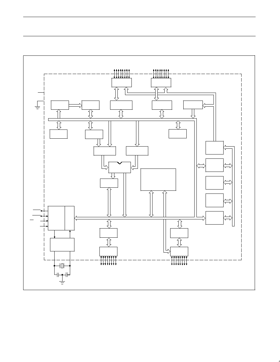
BLOCK DIAGRAM
PSEN
EA/VPP
ALE/PROG
RST
XTAL1
XTAL2
VCC
VSS
PORT 0
DRIVERS
PORT 2
DRIVERS
RAM ADDR
REGISTER
RAM
PORT 0
LATCH
PORT 2
LATCH
ROM/EPROM
REGISTER
B
ACC
STACK
POINTER
TMP2
TMP1
ALU
TIMING
AND
CONTROL
INSTRUCTION
REGISTER
PD
OSCILLATOR
PSW
PORT 1
LATCH
PORT 3
LATCH
PORT 1
DRIVERS
PORT 3
DRIVERS
PROGRAM
ADDRESS
REGISTER
BUFFER
PC
INCRE-
MENTER
PROGRAM
COUNTER
DPTR
P1.0≠P1.7
P3.0≠P3.7
P0.0≠P0.7
P2.0≠P2.7
SFRs
TIMERS
P.C.A
SU00022

Philips Semiconductors
Product specification
87L51FA/87L51FB
CMOS single-chip 3.0V 8-bit microcontrollers
1996 Aug 16
3-153
CERAMIC AND PLASTIC LEADED CHIP CARRIER
PIN FUNCTIONS
LCC
6
1
40
7
17
39
29
18
28
Pin
Function
1
NC*
2
P1.0/T2
3
P1.1/T2EX
4
P1.2/ECI
5
P1.3/CEX0
6
P1.4/CEX1
7
P1.5/CEX2
8
P1.6/CEX3
9
P1.7/CEX4
10
RST
11
P3.0/RxD
12
NC*
13
P3.1/TxD
14
P3.2/INT0
15
P3.3/INT1
Pin
Function
16
P3.4/T0
17
P3.5/T1
18
P3.6/WR
19
P3.7/RD
20
XTAL2
21
XTAL1
22
V
SS
23
NC*
24
P2.0/A8
25
P2.1/A9
26
P2.2/A10
27
P2.3/A11
28
P2.4/A12
29
P2.5/A13
30
P2.6/A14
Pin
Function
31
P2.7/A15
32
PSEN
33
ALE/PROG
34
NC*
35
EA/V
PP
36
P0.7/AD7
37
P0.6/AD6
38
P0.5/AD5
39
P0.4/AD4
40
P0.3/AD3
41
P0.2/AD2
42
P0.1/AD1
43
P0.0/AD0
44
V
CC
SU00023
* DO NOT CONNECT
PLASTIC QUAD FLAT PACK
PIN FUNCTIONS
PQFP
44
34
1
11
33
23
12
22
Pin
Function
1
P1.5/CEX2
2
P1.6/CEX3
3
P1.7/CEX4
4
RST
5
P3.0/RxD
6
NC*
7
P3.1/TxD
8
P3.2/INT0
9
P3.3/INT1
10
P3.4/T0
11
P3.5/T1
12
P3.6/WR
13
P3.7/RD
14
XTAL2
15
XTAL1
Pin
Function
16
V
SS
17
NC*
18
P2.0/A8
19
P2.1/A9
20
P2.2/A10
21
P2.3/A11
22
P2.4/A12
23
P2.5/A13
24
P2.6/A14
25
P2.7/A15
26
PSEN
27
ALE/PROG
28
NC*
29
EA/V
PP
30
P0.7/AD7
Pin
Function
31
P0.6/AD6
32
P0.5/AD5
33
P0.4/AD4
34
P0.3/AD3
35
P0.2/AD2
36
P0.1/AD1
37
P0.0/AD0
38
V
CC
39
NC*
40
P1.0/T2
41
P1.1/T2EX
42
P1.2/ECI
43
P1.3/CEX0
44
P1.4/CEX1
SU00024
* DO NOT CONNECT
PIN DESCRIPTIONS
PIN NUMBER
MNEMONIC
DIP
LCC
QFP
TYPE
NAME AND FUNCTION
V
SS
20
22
16
I
Ground: 0V reference.
V
CC
40
44
38
I
Power Supply: This is the power supply voltage for normal, idle, and power-down operation.
P0.0≠0.7
39≠32
43≠36
37≠30
I/O
Port 0: Port 0 is an open-drain, bidirectional I/O port. Port 0 pins that have 1s written to
them float and can be used as high-impedance inputs. Port 0 is also the multiplexed
low-order address and data bus during accesses to external program and data memory. In
this application, it uses strong internal pull-ups when emitting 1s. Port 0 also outputs the
code bytes during program verification and receives code bytes during EPROM
programming. External pull-ups are required during program verification.
P1.0≠P1.7
1≠8
2≠9
40≠44,
1≠3
I/O
Port 1: Port 1 is an 8-bit bidirectional I/O port with internal pull-ups. Port 1 pins that have 1s
written to them are pulled high by the internal pull-ups and can be used as inputs. As inputs,
port 1 pins that are externally pulled low will source current because of the internal pull-ups.
(See DC Electrical Characteristics: I
IL
). Port 1 also receives the low-order address byte
during program memory verification. Alternate functions include:
1
2
40
I
T2 (P1.0): Timer/Counter 2 external count input/Clockout
2
3
41
I
T2EX (P1.1): Timer/Counter 2 Reload/Capture/Direction Control
3
4
42
I
ECI (P1.2): External Clock Input to the PCA
4
5
43
I/O
CEX0 (P1.3): Capture/Compare External I/O for PCA module 0
5
6
44
I/O
CEX1 (P1.4): Capture/Compare External I/O for PCA module 1
6
7
1
I/O
CEX2 (P1.5): Capture/Compare External I/O for PCA module 2
7
8
2
I/O
CEX3 (P1.6): Capture/Compare External I/O for PCA module 3
8
9
3
I/O
CEX4 (P1.7): Capture/Compare External I/O for PCA module 4
P2.0≠P2.7
21≠28
24≠31
18≠25
I/O
Port 2: Port 2 is an 8-bit bidirectional I/O port with internal pull-ups. Port 2 pins that have 1s
written to them are pulled high by the internal pull-ups and can be used as inputs. As inputs,
port 2 pins that are externally being pulled low will source current because of the internal
pull-ups. (See DC Electrical Characteristics: I
IL
). Port 2 emits the high-order address byte
during fetches from external program memory and during accesses to external data memory
that use 16-bit addresses (MOVX @DPTR). In this application, it uses strong internal
pull-ups when emitting 1s. During accesses to external data memory that use 8-bit addresses
(MOV @Ri), port 2 emits the contents of the P2 special function register. Some Port 2 pins
receive the high order address bits during EPROM programming and verification.

Philips Semiconductors
Product specification
87L51FA/87L51FB
CMOS single-chip 3.0V 8-bit microcontrollers
1996 Aug 16
3-154
PIN DESCRIPTIONS (Continued)
PIN NUMBER
MNEMONIC
DIP
LCC
QFP
TYPE
NAME AND FUNCTION
P3.0≠P3.7
10≠17
11,
13≠19
5,
7≠13
I/O
Port 3: Port 3 is an 8-bit bidirectional I/O port with internal pull-ups. Port 3 pins that have 1s
written to them are pulled high by the internal pull-ups and can be used as inputs. As inputs,
port 3 pins that are externally being pulled low will source current because of the pull-ups.
(See DC Electrical Characteristics: I
IL
). Port 3 also serves the special features of the 80C51
family, as listed below:
10
11
5
I
RxD (P3.0): Serial input port
11
13
7
O
TxD (P3.1): Serial output port
12
14
8
I
INT0 (P3.2): External interrupt
13
15
9
I
INT1 (P3.3): External interrupt
14
16
10
I
T0 (P3.4): Timer 0 external input
15
17
11
I
T1 (P3.5): Timer 1 external input
16
18
12
O
WR (P3.6): External data memory write strobe
17
19
13
O
RD (P3.7): External data memory read strobe
RST
9
10
4
I
Reset: A high on this pin for two machine cycles while the oscillator is running, resets the
device. An internal diffused resistor to V
SS
permits a power-on reset using only an external
capacitor to V
CC
.
ALE/PROG
30
33
27
I/O
Address Latch Enable/Program Pulse: Output pulse for latching the low byte of the
address during an access to external memory. In normal operation, ALE is emitted at a
constant rate of 1/6 the oscillator frequency, and can be used for external timing or clocking.
Note that one ALE pulse is skipped during each access to external data memory. This pin is
also the program pulse input (PROG) during EPROM programming.
PSEN
29
32
26
O
Program Store Enable: The read strobe to external program memory. When the
87L51FA/FB is executing code from the external program memory, PSEN is activated twice
each machine cycle, except that two PSEN activations are skipped during each access to
external data memory. PSEN is not activated during fetches from internal program memory.
EA/V
PP
31
35
29
I
External Access Enable/Programming Supply Voltage: EA must be externally held low
to enable the device to fetch code from external program memory locations 0000H and
1FFFH. If EA is held high, the device executes from internal program memory unless the
program counter contains an address greater than 1FFFH. This pin also receives the
12.75V programming supply voltage (V
PP
) during EPROM programming. If security bit 1 is
programmed, EA will be internally latched on Reset.
XTAL1
19
21
15
I
Crystal 1: Input to the inverting oscillator amplifier and input to the internal clock generator
circuits.
XTAL2
18
20
14
O
Crystal 2: Output from the inverting oscillator amplifier.
NOTE:
To avoid "latch-up" effect at power-on, the voltage on any pin at any time must not be higher than V
CC
+ 0.5V or V
SS
≠ 0.5V, respectively.
TIMER 2
This is a 16-bit up or down counter, which can be operated as either
a timer or event counter. It can be operated in one of three different
modes (autoreload, capture or as the baud rate generator for the
UART).
In the autoreload mode the Timer can be set to count up or down by
setting or clearing the bit DCEN in the T2CON Special Function
Register. The SFR's RCAP2H and RCAP2L are used to reload the
Timer upon overflow or a 1-to-0 transition on the T2EX input (P1.1).
In the Capture mode Timer 2 can either set TF2 and generate an
interrupt or capture its value. To capture Timer 2 in response to a
1-to-0 transition on the T2EX input, the EXEN2 bit in the T2CON
must be set. Timer 2 is then captured in SFR's RCAP2H and
RCAP2L.
As the baud rate generator, Timer 2 is selected by setting TCLK
and/or RCLK in T2CON. As the baud rate generator Timer 2 is
incremented at
1
/
2
the oscillator frequency.
ENHANCED UART
The 87L51FA/FB UART has all of the capabilities of the standard
80C51 UART plus Framing Error Detection and Automatic Address
Recognition. As in the 80C51, all four modes of operation are
supported as well as the 9th bit in modes 2 and 3 that can be used
to facilitate multiprocessor communication.
The Framing Error Detection allows the UART to look for missing
stop bits. If a Stop bit is missing, the FE bit in the SCON SFR is set.
The FE bit can be checked after each transmission to detect
communication errors. The FE bit can only be cleared by software
and is not affected by a valid stop bit.
Automatic Address Recognition is used to reduce the CPU service
time for the serial port. The CPU only needs to service the UART
when it is addressed and, with this done by the on-chip circuitry, the
need for software overhead is greatly reduced. This mode works
similar to the 9-bit communication mode, except that it uses only 8
bits and the Stop bit is used to cause the RI bit to be set. There are
two SFRs associated with this mode. They are SADDR, which holds
the slave address and SADEN, which contains a mask that allows
selective masking of the slave address so that broadcast addresses
can be used.

Philips Semiconductors
Product specification
87L51FA/87L51FB
CMOS single-chip 3.0V 8-bit microcontrollers
1996 Aug 16
3-155
PROGRAMMABLE COUNTER ARRAY
The PCA is a sophisticated free-running 16 bit Timer/Counter that
drives 5 modules that can be individually configured as Capture
inputs, software timers, high speed outputs, or pulse width
modulated outputs. In addition, module 4 can be configured as a
software controlled watchdog timer.
The Timer portion of the PCA can be configured to run in one of four
different modes. The modes are:
1
/
2
the oscillator frequency,
1
/
4
the
oscillator frequency, Timer 0 overflows, or from the ECI input.
For the Capture/Compare mode each of the modules has a pair of
registers associated with it called CCAPnH and CCAPnL (where
n = 0, 1, 2, 3, 4 depending on the module). Both positive and
negative transitions can be captured. This means that the PCA has
the flexibility to measure phase differences, duty cycles, pulse
widths and a wide variety of other digital pulse characteristics.
In the 16-bit software timer mode each of the modules can generate
an interrupt upon a compare.
For applications that require accurate pulse widths and edges the
PCA modules can be used as High Speed Outputs (HSO). The PCA
toggles the appropriate CEXn pin when there is a match between
the PCA timer and the modules compare registers.
The pulse width modulator mode for the PCA allows the conversion
of digital information into analog signals. Each of the 5 modules can
be used in this mode. The frequency of the PWM depends on the
clock source for the PCA. The 8-bit PWM output is generated by
comparing the low byte of the PCA (CL) with the module's CCAPnL
SFR. When CL < CCAPnL, the output is high. When CL > CCAPnL,
the output is low.
POWER OFF FLAG
The Power Off Flag (POF) is set by on-chip circuitry when the V
CC
level on the 87L51FA/FB rises from 0 to 3.3V. The POF bit can be
set or cleared by software allowing a user to determine if the reset is
the result of a power-on or a warm start after powerdown. The V
CC
level must remain above 2.0V for the POF to remain unaffected by
the V
CC
level.
OSCILLATOR CHARACTERISTICS
XTAL1 and XTAL2 are the input and output, respectively, of an
inverting amplifier. The pins can be configured for use as an on-chip
oscillator.
To drive the device from an external clock source, XTAL1 should be
driven while XTAL2 is left unconnected. There are no requirements
on the duty cycle of the external clock signal, because the input to
the internal clock circuitry is through a divide-by-two flip-flop.
However, minimum and maximum high and low times specified in
the data sheet must be observed.
Reset
A reset is accomplished by holding the RST pin high for at least two
machine cycles (24 oscillator periods), while the oscillator is running.
To insure a good power-on reset, the RST pin must be high long
enough to allow the oscillator time to start up (normally a few
milliseconds) plus two machine cycles. At power-on, the voltage on
V
CC
and RST must come up at the same time for a proper start-up.
Idle Mode
In the idle mode, the CPU puts itself to sleep while all of the on-chip
peripherals stay active. The instruction to invoke the idle mode is the
last instruction executed in the normal operating mode before the
idle mode is activated. The CPU contents, the on-chip RAM, and all
of the special function registers remain intact during this mode. The
idle mode can be terminated either by any enabled interrupt (at
which time the process is picked up at the interrupt service routine
and continued), or by a hardware reset which starts the processor in
the same manner as a power-on reset.
Power-Down Mode
To save even more power, a Power Down mode can be invoked by
software. In this mode, the oscillator is stopped and the instruction
that invoked Power Down is the last instruction executed. The
on-chip RAM and Special Function Registers retain their values until
the Power Down mode is terminated.
On the 87L51FA/FB either a hardware reset or external interrupt can
use an exit from Power Down. Reset redefines all the SFRs but
does not change the on-chip RAM. An external interrupt allows both
the SFRs and the on-chip RAM to retain their values.
To properly terminate Power Down the reset or external interrupt
should not be executed before V
CC
is restored to its normal
operating level and must be held active long enough for the
oscillator to restart and stabilize (normally less than 10ms).
With an external interrupt, INT0 and INT1 must be enabled and
configured as level-sensitive. Holding the pin low restarts the
oscillator but bringing the pin back high completes the exit. Once the
interrupt is serviced, the next instruction to be executed after RETI
will be the one following the instruction that put the device into
Power Down.
Design Consideration
∑
When the idle mode is terminated by a hardware reset, the device
normally resumes program execution, from where it left off, up to
two machine cycles before the internal rest algorithm takes
control. On-chip hardware inhibits access to internal RAM in this
event, but access to the port pins is not inhibited. To eliminate the
possibility of an unexpected write when Idle is terminated by reset,
the instruction following the one that invokes Idle should not be
one that writes to a port pin or to external memory.
ONCE
TM
Mode
The ONCE ("On-Circuit Emulation") Mode facilitates testing and
debugging of systems using the 87L51FA/FB without the
87L51FA/FB having to be removed from the circuit. The ONCE
Mode is invoked by:
1. Pull ALE low while the device is in reset and PSEN is high;
2. Hold ALE low as RST is deactivated.
While the device is in ONCE Mode, the Port 0 pins go into a float
state, and the other port pins and ALE and PSEN are weakly pulled
high. The oscillator circuit remains active. While the 87L51FA/FB is
in this mode, an emulator or test CPU can be used to drive the
circuit. Normal operation is restored when a normal reset is applied.

Philips Semiconductors
Product specification
87L51FA/87L51FB
CMOS single-chip 3.0V 8-bit microcontrollers
1996 Aug 16
3-156
Table 1. External Pin Status During Idle and Power-Down Mode
MODE
PROGRAM
MEMORY
ALE
PSEN
PORT 0
PORT 1
PORT 2
PORT 3
Idle
Internal
1
1
Data
Data
Data
Data
Idle
External
1
1
Float
Data
Address
Data
Power-down
Internal
0
0
Data
Data
Data
Data
Power-down
External
0
0
Float
Data
Data
Data
ABSOLUTE MAXIMUM RATINGS
1, 2, 3
PARAMETER
RATING
UNIT
Operating temperature under bias
0 to +70 or ≠40 to +85
∞
C
Storage temperature range
≠65 to +150
∞
C
Voltage on EA/V
PP
pin to V
SS
0 to +13.0
V
Voltage on any other pin to V
SS
≠0.5 to +6.5
V
Maximum I
OL
per I/O pin
15
mA
Power dissipation (based on package heat transfer limitations, not
device power consumption)
1.5
W
NOTES:
1. Stresses above those listed under Absolute Maximum Ratings may cause permanent damage to the device. This is a stress rating only and
functional operation of the device at these or any conditions other than those described in the AC and DC Electrical Characteristics section
of this specification is not implied.
2. This product includes circuitry specifically designed for the protection of its internal devices from the damaging effects of excessive static
charge. Nonetheless, it is suggested that conventional precautions be taken to avoid applying greater than the rated maxima.
3. Parameters are valid over operating temperature range unless otherwise specified. All voltages are with respect to V
SS
unless otherwise
noted.
Electrical Deviations from Commercial Specifications for Extended Temperature Range
DC and AC parameters not included here are the same as in the commercial temperature range table.
Philips Semiconductors
Product specification
87L51FA/87L51FB
CMOS single-chip 3.0V 8-bit microcontrollers
1996 Aug 16
3-157
DC ELECTRICAL CHARACTERISTICS
T
amb
= 0
∞
C to +70
∞
C, ≠40 to +85
∞
C, V
CC
= 3.0V to 4.5V, V
SS
= 0V
TEST
LIMITS
SYMBOL
PARAMETER
CONDITIONS
MIN
TYP
1
MAX
UNIT
V
IL
Input low voltage, except EA
2,3
≠0.5
0.8
V
V
IL1
Input low voltage to EA
2,3
0
0.8
V
V
IH
Input high voltage, except XTAL1, RST
2,4
2.0
V
CC
+0.5
V
V
IH1
Input high voltage, XTAL1, RST
2,4
0.7V
CC
V
CC
+0.5
V
V
OL
Output low voltage, ports 1, 2, 3
5
I
OL
= 1.6mA
6
0.45
V
V
OL1
Output low voltage, port 0, ALE, PSEN
5
I
OL
= 3.2mA
6
0.45
V
V
OH
Output high voltage, ports 1, 2, 3, ALE, PSEN
7
I
OH
= ≠20
µ
A
V
CC
≠ 0.5
V
V
OH1
Output high voltage (port 0 in external bus mode),
ALE
8
, PSEN
7
I
OH
= ≠3.2mA
V
CC
≠ 0.7
V
I
IL
Logical 0 input current, ports 1, 2, 3
2
V
IN
= 0.4V
≠50
µ
A
I
TL
Logical 1-to-0 transition current, ports 1, 2, 3
2
See note 9
≠650
µ
A
I
LI
Input leakage current, port 0
0.45 V
IN
< V
CC
≠ 0.3
±
10
µ
A
I
CC
Power supply current:2
Active mode @ 20MHz
10
Idle mode @ 20MHz
Power-down mode
See note 11
9
2
10
22
6
75
mA
mA
µ
A
R
RST
Internal reset pull-down resistor
40
225
k
C
IO
Pin capacitance
12
(except EA)
15
pF
NOTES:
1. Typical ratings are not guaranteed. The values listed are at room temperature, 3.3V.
2. These values apply only to T
amb
= 0
∞
C to +70
∞
C.
3. For V
CC
voltages above 3.6V and less than 5.5V, V
IL
= 0.3V
CC
≠ 0.1
4. For V
CC
voltages above 3.6V and less than 5.5V, V
IH
= 0.3V
CC
+ 0.92
5. Under steady state (non-transient) conditions, I
OL
must be externally limited as follows:
Maximum I
OL
per port pin:
15mA (*NOTE: This is 85
∞
C specification.)
Maximum I
OL
per 8-bit port:
26mA
Maximum total I
OL
for all outputs:
71mA
If I
OL
exceeds the test condition, V
OL
may exceed the related specification. Pins are not guaranteed to sink current greater than the listed
test conditions.
6. Capacitive loading on ports 0 and 2 may cause spurious noise to be superimposed on the V
OL
s of ALE and ports 1 and 3. The noise is due
to external bus capacitance discharging into the port 0 and port 2 pins when these pins make 1-to-0 transitions during bus operations. In the
worst cases (capacitive loading > 100pF), the noise pulse on the ALE pin may exceed 0.8V. In such cases, it may be desirable to qualify
ALE with a Schmitt Trigger, or use an address latch with a Schmitt Trigger STROBE input. I
OL
can exceed these conditions provided that no
single output sinks more than 5mA and no more than two outputs exceed the test conditions.
7. Capacitive loading on ports 0 and 2 may cause the V
OH
on ALE and PSEN to momentarily fall below the 0.9V
CC
specification when the
address bits are stabilizing.
8. ALE is tested to V
OH1
, except when ALE is off then V
OH
is the voltage specification.
9. Pins of ports 1, 2 and 3 source a transition current when they are being externally driven from 1 to 0. The transition current reaches its
maximum value when V
IN
is approximately 1.5V.
10. I
CCMAX
at other frequencies is given by: Active mode: I
CCMAX
= 0.8
◊
FREQ + 6: Idle mode: I
CCMAX
= 0.19
◊
FREQ +2.50,
where FREQ is the external oscillator frequency in MHz. I
CCMAX
is given in mA. See Figure 8.
11. See Figures 9 through 12 for I
CC
test conditions.
12. Pin capacitance is less than 25pF. Pin capacitance of ceramic package is less than 15pF (except EA is 25pF). These values are
guaranteed by design and are not tested.
Philips Semiconductors
Product specification
87L51FA/87L51FB
CMOS single-chip 3.0V 8-bit microcontrollers
1996 Aug 16
3-158
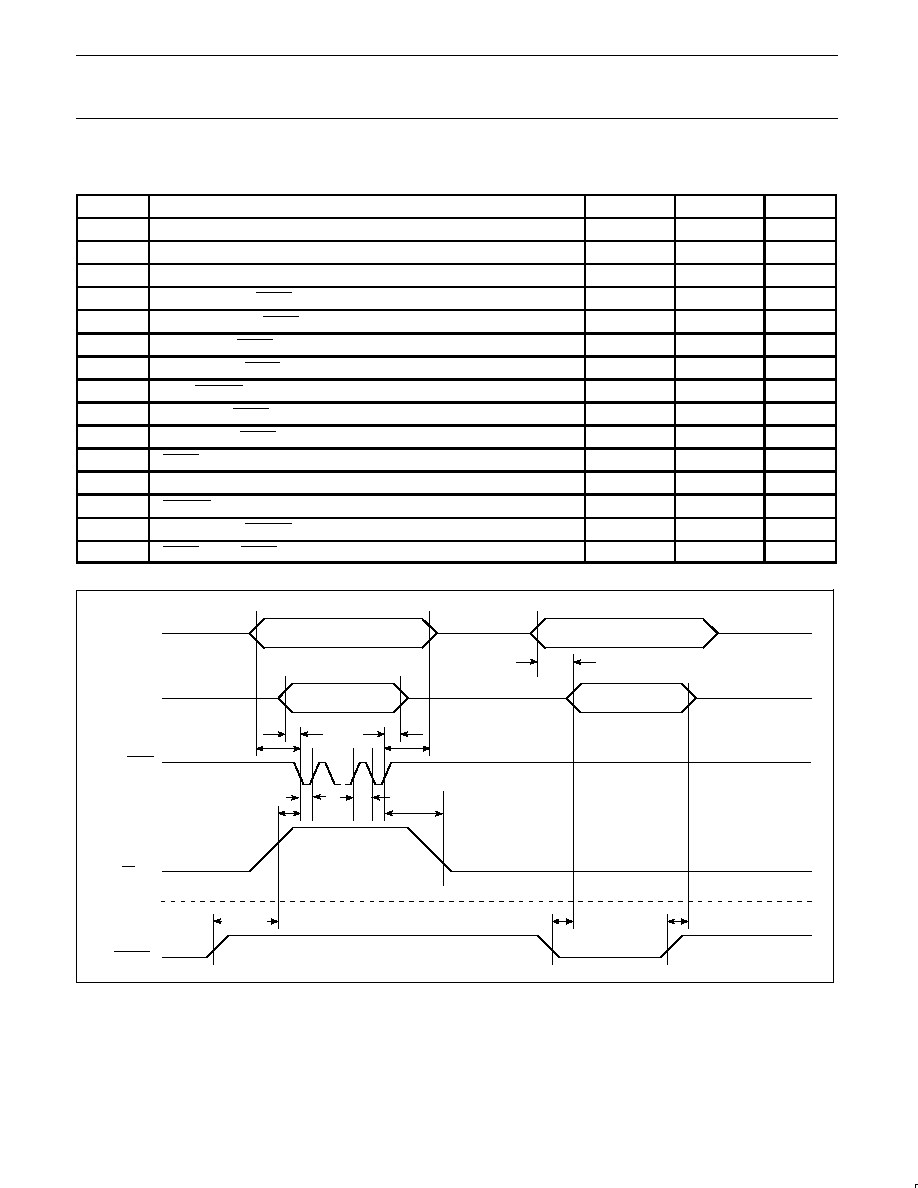
AC ELECTRICAL CHARACTERISTICS
T
amb
= 0
∞
C to +70
∞
C, ≠40 to +85
∞
C, V
CC
= 3.0V to 4.5V, V
SS
= 0V
1, 2, 3
16MHz CLOCK
VARIABLE CLOCK
SYMBOL
FIGURE
PARAMETER
MIN
MAX
MIN
MAX
UNIT
1/t
CLCL
1
Oscillator frequency
≠4, ≠5
3.5
16
MHz
≠7, ≠8
3.5
20
MHz
t
LHLL
1
ALE pulse width
85
2t
CLCL
≠40
ns
t
AVLL
1
Address valid to ALE low
22
t
CLCL
≠40
ns
t
LLAX
1
Address hold after ALE low
32
t
CLCL
≠30
ns
t
LLIV
1
ALE low to valid instruction in
150
4t
CLCL
≠100
ns
t
LLPL
1
ALE low to PSEN low
32
t
CLCL
≠30
ns
t
PLPH
1
PSEN pulse width
142
3t
CLCL
≠45
ns
t
PLIV
1
PSEN low to valid instruction in
82
3t
CLCL
≠105
ns
t
PXIX
1
Input instruction hold after PSEN
0
0
ns
t
PXIZ
1
Input instruction float after PSEN
37
t
CLCL
≠25
ns
t
AVIV
1
Address to valid instruction in
207
5t
CLCL
≠105
ns
t
PLAZ
1
PSEN low to address float
10
10
ns
Data Memory
t
RLRH
2, 3
RD pulse width
275
6t
CLCL
≠100
ns
t
WLWH
2, 3
WR pulse width
275
6t
CLCL
≠100
ns
t
RLDV
2, 3
RD low to valid data in
147
5t
CLCL
≠165
ns
t
RHDX
2, 3
Data hold after RD
0
0
ns
t
RHDZ
2, 3
Data float after RD
65
2t
CLCL
≠60
ns
t
LLDV
2, 3
ALE low to valid data in
350
8t
CLCL
≠150
ns
t
AVDV
2, 3
Address to valid data in
397
9t
CLCL
≠165
ns
t
LLWL
2, 3
ALE low to RD or WR low
137
237
3t
CLCL
≠50
3t
CLCL
+50
ns
t
AVWL
2, 3
Address valid to WR low or RD low
122
4t
CLCL
≠130
ns
t
QVWX
2, 3
Data valid to WR transition
13
t
CLCL
≠50
ns
t
WHQX
2, 3
Data hold after WR
13
t
CLCL
≠50
ns
t
QVWH
3
Data valid to WR high
287
7t
CLCL
≠150
ns
t
RLAZ
2, 3
RD low to address float
0
0
ns
t
WHLH
2, 3
RD or WR high to ALE high
23
103
t
CLCL
≠40
t
CLCL
+40
ns
External Clock
t
CHCX
5
High time
12
20
ns
t
CLCX
5
Low time
12
20
ns
t
CLCH
5
Rise time
20
20
ns
t
CHCL
5
Fall time
20
20
ns
Shift Register
t
XLXL
4
Serial port clock cycle time
1
12t
CLCL
µ
s
t
QVXH
4
Output data setup to clock rising edge
492
10t
CLCL
≠133
ns
t
XHQX
4
Output data hold after clock rising edge
8
2t
CLCL
≠117
ns
t
XHDX
4
Input data hold after clock rising edge
0
0
ns
t
XHDV
4
Clock rising edge to input data valid
492
10t
CLCL
≠133
ns
NOTES:
1. Parameters are valid over operating temperature range unless otherwise specified.
2. Load capacitance for port 0, ALE, and PSEN = 100pF, load capacitance for all other outputs = 80pF.
3. Interfacing the 87L51FA/FB to devices with float times up to 45ns is permitted. This limited bus contention will not cause damage to Port 0
drivers.
Philips Semiconductors
Product specification
87L51FA/87L51FB
CMOS single-chip 3.0V 8-bit microcontrollers
1996 Aug 16
3-159
EXPLANATION OF THE AC SYMBOLS
Each timing symbol has five characters. The first character is always
`t' (= time). The other characters, depending on their positions,
indicate the name of a signal or the logical status of that signal. The
designations are:
A ≠ Address
C ≠ Clock
D ≠ Input data
H ≠ Logic level high
I ≠ Instruction (program memory contents)
L ≠ Logic level low, or ALE
P ≠ PSEN
Q ≠ Output data
R ≠ RD signal
t ≠ Time
V ≠ Valid
W ≠ WR signal
X ≠ No longer a valid logic level
Z ≠ Float
Examples: t
AVLL
= Time for address valid to ALE low.
t
LLPL
= Time for ALE low to PSEN low.
t
PXIZ
ALE
PSEN
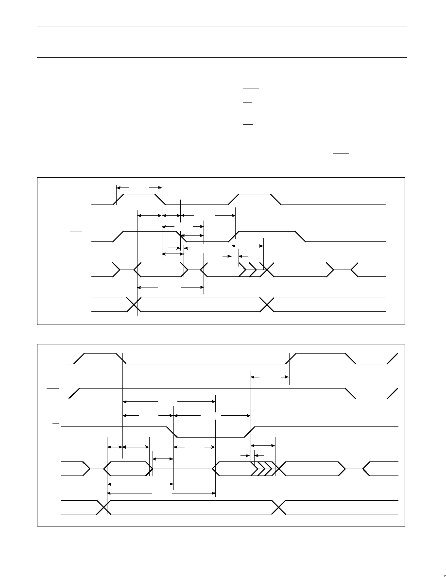
PORT 0
PORT 2
A0≠A15
A8≠A15
A0≠A7
A0≠A7
t
AVLL
t
PXIX
t
LLAX
INSTR IN
t
PLIV
t
LHLL
t
PLPH
t
LLIV
t
PLAZ
t
LLPL
t
AVIV
SU00056
Figure 1. External Program Memory Read Cycle
ALE
PSEN
PORT 0
PORT 2
RD
A0≠A7
FROM RI OR DPL
DATA IN
A0≠A7 FROM PCL
INSTR IN
P2.0≠P2.7 OR A8≠A15 FROM DPF
A0≠A15 FROM PCH
t
WHLH
t
LLDV
t
LLWL
t
RLRH
t
LLAX
t
RLAZ
t
AVLL
t
RHDX
t
RHDZ
t
AVWL
t
AVDV
t
RLDV
SU00025
Figure 2. External Data Memory Read Cycle

Philips Semiconductors
Product specification
87L51FA/87L51FB
CMOS single-chip 3.0V 8-bit microcontrollers
1996 Aug 16
3-160
t
LLAX
ALE
PSEN
PORT 0
PORT 2
WR
A0≠A7
FROM RI OR DPL
DATA OUT
A0≠A7 FROM PCL
INSTR IN
P2.0≠P2.7 OR A8≠A15 FROM DPF
A0≠A15 FROM PCH
t
WHLH
t
LLWL
t
WLWH
t
AVLL
t
AVWL
t
QVWX
t
WHQX
t
QVWH
SU00026
Figure 3. External Data Memory Write Cycle
0
1
2
3
4
5
6
7
8
INSTRUCTION
ALE
CLOCK
OUTPUT DATA
WRITE TO SBUF
INPUT DATA
CLEAR RI
VALID
VALID
VALID
VALID
VALID
VALID
VALID
VALID
SET TI
SET RI
t
XLXL
t
QVXH
t
XHQX
t
XHDX
t
XHDV
SU00027
1
2
3
0
4
5
6
7
Figure 4. Shift Register Mode Timing
VCC≠0.5
0.45V
0.7VCC
0.2VCC≠0.1
t
CHCL
t
CLCL
t
CLCH
t
CLCX
t
CHCX
SU00009
Figure 5. External Clock Drive
Philips Semiconductors
Product specification
87L51FA/87L51FB
CMOS single-chip 3.0V 8-bit microcontrollers
1996 Aug 16
3-161
VCC≠0.3
0.3V
0.3VCC+0.92
0.3VCC≠0.1
NOTE:
AC inputs during testing are driven at V
CC
≠0.3 for a logic `1' and 0.3V for a logic `0'.
Timing measurements are made at V
IH
min for a logic `1' and V
IL
for a logic `0'.
SU00051
Figure 6. AC Testing Input/Output
VLOAD
VLOAD+0.1V
VLOAD≠0.1V
VOH≠0.1V
VOL+0.1V
NOTE:
TIMING
REFERENCE
POINTS
For timing purposes, a port is no longer floating when a 100mV change from load voltage occurs,
and begins to float when a 100mV change from the loaded V
OH
/V
OL
level occurs. I
OH
/I
OL
±
20mA.
SU00011
Figure 7. Float Waveform
25
20
15
10
5
4MHz
8MHz
12MHz
16MHz
FREQ AT XTAL1
MAX ACTIVE MODE
TYP ACTIVE MODE
MAX IDLE MODE
TYP IDLE MODE
ICC mA
IDDMAX = 0.8 X FREQ. + 6.0
Note: 3.3V operation will reduce I
CC
vs. XTAL frequency. This curve will
change as characterization data be-
comes available.
20MHz
IDDIDLE = 0.19 X FREQ. + 2.5
SU00052
Figure 8. I
CC
vs. FREQ Valid only within frequency specifications of the device under test
Philips Semiconductors
Product specification
87L51FA/87L51FB
CMOS single-chip 3.0V 8-bit microcontrollers
1996 Aug 16
3-162
V
CC
P0
EA
RST
XTAL1
XTAL2
V
SS
V
CC
V
CC
V
CC
I
CC
(NC)
CLOCK SIGNAL
SU00719
Figure 9. I
CC
Test Condition, Active Mode
All other pins are disconnected
V
CC
P0
EA
RST
XTAL1
XTAL2
V
SS
V
CC
V
CC
I
CC
(NC)
CLOCK SIGNAL
SU00720
Figure 10. I
CC
Test Condition, Idle Mode
All other pins are disconnected
VCC≠0.5
0.45V
0.7VCC
0.2VCC≠0.1
t
CHCL
t
CLCL
t
CLCH
t
CLCX
t
CHCX
SU00009
Figure 11. Clock Signal Waveform for I
CC
Tests in Active and Idle Modes
t
CLCH
= t
CHCL
= 5ns
V
CC
P0
EA
RST
XTAL1
XTAL2
VSS
V
CC
V
CC
I
CC
(NC)
SU00016
Figure 12. I
CC
Test Condition, Power Down Mode
All other pins are disconnected. V
CC
= 2V to 4.5V
Philips Semiconductors
Product specification
87L51FA/87L51FB
CMOS single-chip 3.0V 8-bit microcontrollers
1996 Aug 16
3-163
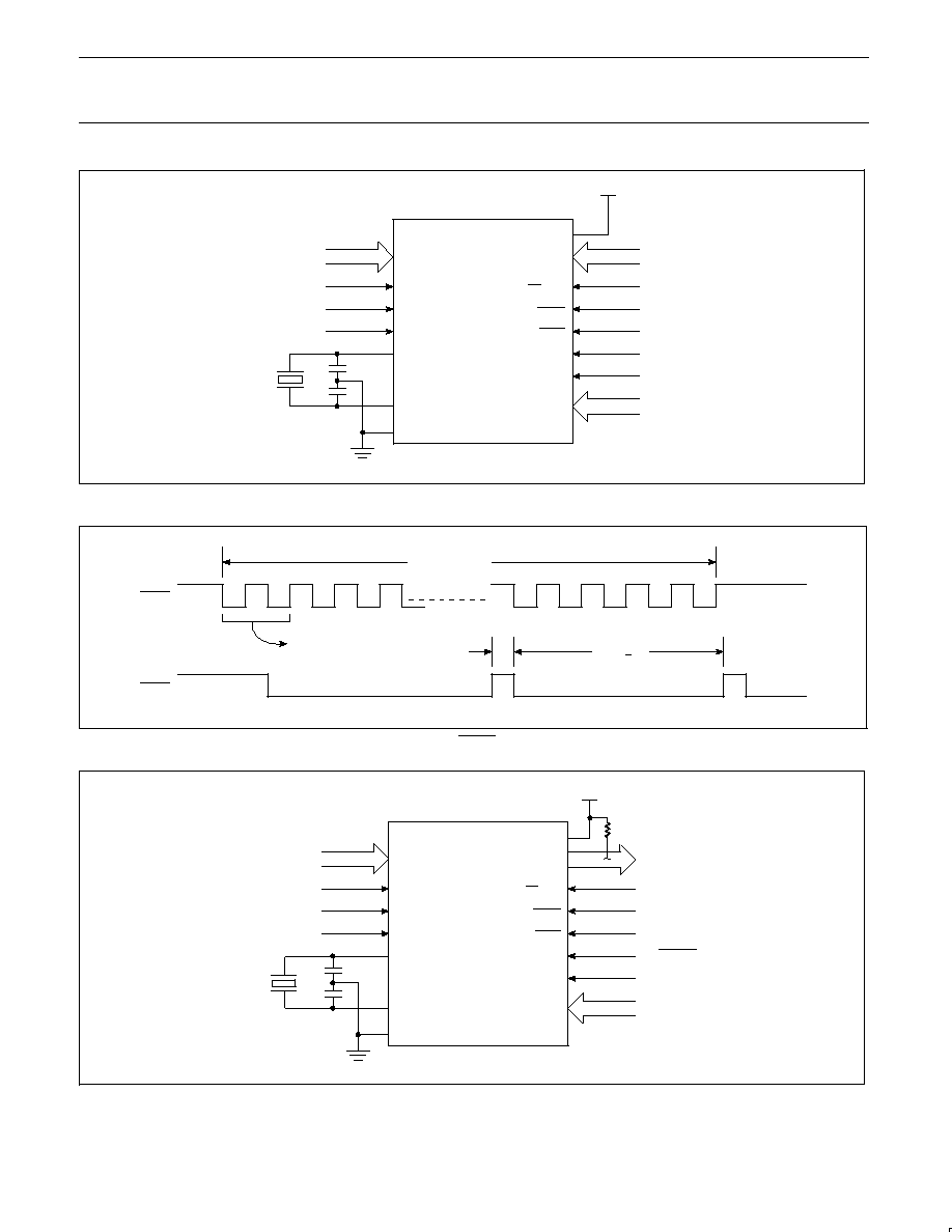
EPROM CHARACTERISTICS
The 87L51FA/FB is programmed by using a modified Quick-Pulse
Programming
TM
algorithm. It differs from older methods in the value
used for V
PP
(programming supply voltage) and in the width and
number of the ALE/PROG pulses.
The 87L51FA/FB contains two signature bytes that can be read and
used by an EPROM programming system to identify the device. The
signature bytes identify the device as an 87L51FA/FB manufactured
by Philips.
Table 2 shows the logic levels for reading the signature byte, and for
programming the program memory, the encryption table, and the
security bits. The circuit configuration and waveforms for quick-pulse
programming are shown in Figures 13 and 14. Figure 15 shows the
circuit configuration for normal program memory verification.
Quick-Pulse Programming
The setup for microcontroller quick-pulse programming is shown in
Figure 13. Note that the 87L51FA/FB is running with a 4 to 6MHz
oscillator. The reason the oscillator needs to be running is that the
device is executing internal address and program data transfers.
The address of the EPROM location to be programmed is applied to
ports 1 and 2, as shown in Figure 13. The code byte to be
programmed into that location is applied to port 0. RST, PSEN and
pins of ports 2 and 3 specified in Table 2 are held at the `Program
Code Data' levels indicated in Table 2. The ALE/PROG is pulsed
low from 5 to 25 times as shown in Figure 14.
To program the encryption table, repeat the 5 to 25 pulse
programming sequence for addresses 0 through 1FH, using the
`Pgm Encryption Table' levels. Do not forget that after the encryption
table is programmed, verification cycles will produce only encrypted
data.
To program the security bits, repeat the 5 to 25 pulse programming
sequence using the `Pgm Security Bit' levels. After one security bit is
programmed, further programming of the code memory and
encryption table is disabled. However, the other security bit can still
be programmed.
Note that the EA/V
PP
pin must not be allowed to go above the
maximum specified V
PP
level for any amount of time. Even a narrow
glitch above that voltage can cause permanent damage to the
device. The V
PP
source should be well regulated and free of glitches
and overshoot.
Program Verification
If security bit 2 has not been programmed, the on-chip program
memory can be read out for program verification. The address of the
program memory locations to be read is applied to ports 1 and 2 as
shown in Figure 15. The other pins are held at the `Verify Code Data'
levels indicated in Table 2. The contents of the address location will
be emitted on port 0. External pull-ups are required on port 0 for this
operation.
If the encryption table has been programmed, the data presented at
port 0 will be the exclusive NOR of the program byte with one of the
encryption bytes. The user will have to know the encryption table
contents in order to correctly decode the verification data. The
encryption table itself cannot be read out.
Reading the Signature Bytes
The signature bytes are read by the same procedure as a normal
verification of locations 030H and 031H, except that P3.6 and P3.7
need to be pulled to a logic low. The values are:
(030H) = 15H indicates manufactured by Philips
(031H) = B1H indicates 87L51FA
= B2H indicates 87L51FB
Program/Verify Algorithms
Any algorithm in agreement with the conditions listed in Table 2, and
which satisfies the timing specifications, is suitable.
Erasure Characteristics
Erasure of the EPROM begins to occur when the chip is exposed to
light with wavelengths shorter than approximately 4,000 angstroms.
Since sunlight and fluorescent lighting have wavelengths in this
range, exposure to these light sources over an extended time (about
1 week in sunlight, or 3 years in room level fluorescent lighting)
could cause inadvertent erasure. For this and secondary effects,
it is recommended that an opaque label be placed over the
window. For elevated temperature or environments where solvents
are being used, apply Kapton tape Fluorglas part number 2345≠5, or
equivalent.
The recommended erasure procedure is exposure to ultraviolet light
(at 2537 angstroms) to an integrated dose of at least 15W-s/cm
2
.
Exposing the EPROM to an ultraviolet lamp of 12,000
µ
W/cm
2
rating
for 20 to 39 minutes, at a distance of about 1 inch, should be
sufficient.
Erasure leaves the array in an all 1s state.
Table 2. EPROM Programming Modes
1,2,3
MODE
RST
PSEN
ALE/PROG
EA/V
PP
P2.7
P2.6
P3.7
P3.6
Read signature
1
0
1
1
0
0
0
0
Program code data
1
0
0
4
V
PP
1
0
1
1
Verify code data
1
0
1
1
0
0
1
1
Pgm encryption table
1
0
0
4
V
PP
1
0
1
0
Pgm security bit 1
1
0
0
4
V
PP
1
1
1
1
Pgm security bit 2
1
0
0
4
V
PP
1
1
0
0
NOTES:
1. `0' = Valid low for that pin, `1' = valid high for that pin.
2. V
PP
= 12.75V
±
0.25V.
3. V
CC
= 5V
±
10% during programming and verification.
4. ALE/PROG receives 5 to 25 programming pulses while V
PP
is held at 12.75V. Each programming pulse is low for 100
µ
s (
±
10
µ
s) and high for
a minimum of 10
µ
s.
TM
Trademark phrase of Intel Corporation.
Philips Semiconductors
Product specification
87L51FA/87L51FB
CMOS single-chip 3.0V 8-bit microcontrollers
1996 Aug 16
3-164
A0≠A7
1
1
1
4≠6MHz
+5V
PGM DATA
+12.75V
25 100
µ
s PULSES TO GROUND
0
1
0
A8≠A13
P1
RST
P3.6
P3.7
XTAL2
XTAL1
VSS
VCC
P0
EA/VPP
ALE/PROG
PSEN
P2.7
P2.6
P2.0≠P2.5
87L51FA
87L51FB
SU00053A
Figure 13. Programming Configuration
ALE/PROG:
ALE/PROG:
1
0
1
0
5 to 25 PULSES
100
µ
s+10
10
µ
s MIN
SU00054
Figure 14. PROG Waveform
A0≠A7
1
1
1
4≠6MHz
+5V
PGM DATA
1
1
0
0 ENABLE
0
A8≠A12
P1
RST
P3.6
P3.7
XTAL2
XTAL1
VSS
VCC
P0
EA/VPP
ALE/PROG
PSEN
P2.7
P2.6
P2.0≠P2.4
87L51FA
87L51FB
SU00055A
Figure 15. Program Verification
Philips Semiconductors
Product specification
87L51FA/87L51FB
CMOS single-chip 3.0V 8-bit microcontrollers
1996 Aug 16
3-165
EPROM PROGRAMMING AND VERIFICATION CHARACTERISTICS
T
amb
= 21
∞
C to +27
∞
C, V
CC
= 5V
±
10%, V
SS
= 0V (See Figure 16)
SYMBOL
PARAMETER
MIN
MAX
UNIT
V
PP
Programming supply voltage
12.5
13.0
V
I
PP
Programming supply current
50
mA
1/t
CLCL
Oscillator frequency
4
6
MHz
t
AVGL
Address setup to PROG low
48t
CLCL
t
GHAX
Address hold after PROG
48t
CLCL
t
DVGL
Data setup to PROG low
48t
CLCL
t
GHDX
Data hold after PROG
48t
CLCL
t
EHSH
P2.7 (ENABLE) high to V
PP
48t
CLCL
t
SHGL
V
PP
setup to PROG low
10
µ
s
t
GHSL
V
PP
hold after PROG
10
µ
s
t
GLGH
PROG width
90
110
µ
s
t
AVQV
Address to data valid
48t
CLCL
t
ELQZ
ENABLE low to data valid
48t
CLCL
t
EHQZ
Data float after ENABLE
0
48t
CLCL
t
GHGL
PROG high to PROG low
10
µ
s
PROGRAMMING
*
VERIFICATION
*
ADDRESS
ADDRESS
DATA IN
DATA OUT
LOGIC 1
LOGIC 1
LOGIC 0
t
AVQV
t
EHQZ
t
ELQV
t
SHGL
t
GHSL
t
GLGH
t
GHGL
t
AVGL
t
GHAX
t
DVGL
t
GHDX
P1.0≠P1.7
P2.0≠P2.4
PORT 0
ALE/PROG
EA/V
PP
P2.7
ENABLE
SU00020
t
EHSH
NOTE:
*
FOR PROGRAMMING VERIFICATION SEE FIGURE 13.
FOR VERIFICATION CONDITIONS SEE FIGURE 15.
Figure 16. EPROM Programming and Verification