 | –≠–ª–µ–∫—Ç—Ä–æ–Ω–Ω—ã–π –∫–æ–º–ø–æ–Ω–µ–Ω—Ç: SA3601 | –°–∫–∞—á–∞—Ç—å:  PDF PDF  ZIP ZIP |

Philips
Semiconductors
SA3601
Low voltage dual-band RF front-end
Preliminary specification
1999 Nov 09
INTEGRATED CIRCUITS
Philips Semiconductors
Preliminary specification
SA3601
Low voltage dual-band RF front-end
2
1999 Nov 09
DESCRIPTION
The SA3601 is an integrated dual-band RF front-end that operates at
both cellular (AMPS and TDMA) and PCS (TDMA) frequencies, and
is designed in a 20 GHz f
T
BiCMOS process--QUBiC2. The
low-band (LB) receiver is a combined low-noise amplifier (LNA) and
mixer. The LNA has a 1.7 dB noise figure (NF) at 881 MHz with 17 dB
of gain and an IIP3 of ≠7 dBm. The wide-dynamic range mixer has a
9.5 dB NF at 881 MHz with 9.5 dB of gain and an IIP3 of +6 dBm.
The high-band (HB) receiver is a combined low-noise amplifier (LNA)
and mixer, with the low-band and high-band mixers sharing the same
mixer output. The LNA has a 2.2 dB NF at 1960 MHz with 16 dB of
gain and an IIP3 of ≠5 dBm. The wide-dynamic range mixer has a
8.5 dB NF at 1960 MHz with 8.5 dB of gain and an IIP3 of +5.5 dBm.
FEATURES
∑
Low current consumption: LB I
CC
= 14 mA; HB I
CC
= 15.5 mA
∑
Outstanding low- and high-band noise figure
∑
LNAs with gain control (30 dB gain step)
∑
LO input and output buffers
∑
Frequency doubler
∑
On chip logic for network selection and power down
∑
Very small outline package
APPLICATIONS
∑
800 to 1000 MHz analog and digital receivers
∑
1800 to 2000 MHz digital receivers
∑
Portable radios
∑
Mobile communications equipment
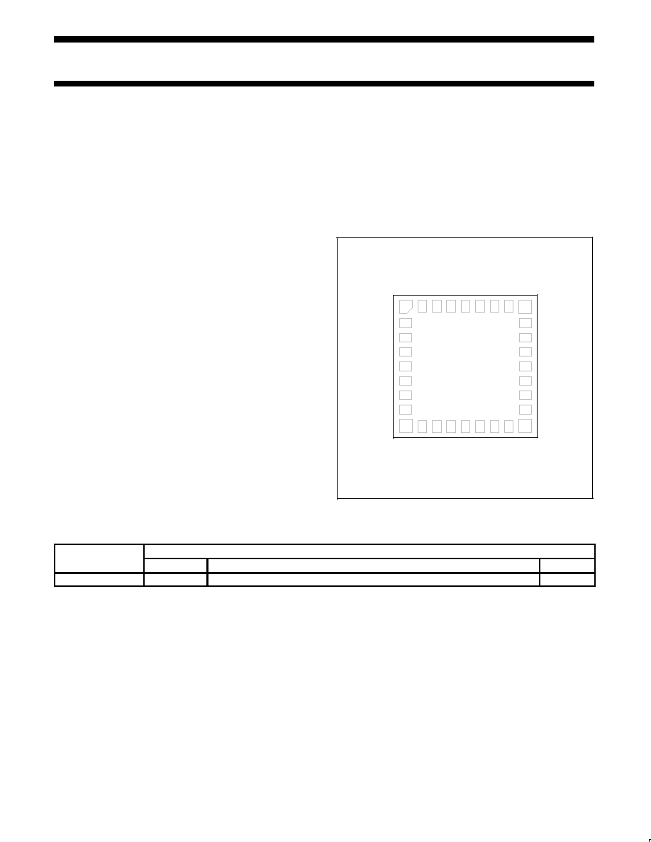
PIN CONFIGURATION
2
3
4
5
6
7
8
TOP VIEW
1
9
10
11
12
13
14
15
16
17
18
19
20
21
22
23
24
25
26
27
28
29
30
31
32
HBLNA_IN
GND
HBMXR+_IN
HBMXR≠_IN
PD1
GND
PD2
GND
GND
LBVCO_OUT
GND
HBVCO_IN
PD3
GND
LBLNA_IN
GND
LBMXR_IN
GND
MXR+_OUT
MXR≠_OUT
GND
LBVCO_IN
GND
GND
HBLNA_OUT
GND
LBLNA_OUT
GND
GND
V
CC
V
CC
V
CC
SR02237
ORDERING INFORMATION
TYPE NUMBER
PACKAGE
TYPE NUMBER
NAME
DESCRIPTION
VERSION
SA3601
BCC32++
HBCC32:
plastic, heatsink bottom chip carrier; 32 terminals; body 5 x 5 x 0.65 mm
SOT560-1

Philips Semiconductors
Preliminary specification
SA3601
Low voltage dual-band RF front-end
1999 Nov 09
3
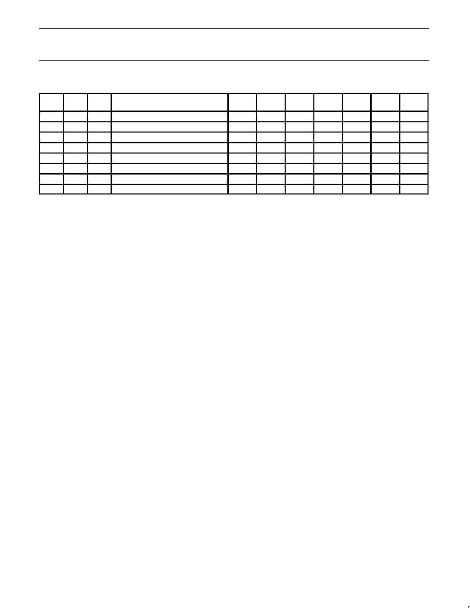
PIN DESCRIPTIONS
PIN
NO.
PIN NAME
DESCRIPTION
1
HBLNA_IN
Highband LNA input
2
GND
Ground
3
V
CC
Power supply
4
HBMXR+_IN
Highband mixer positive input
5
HBMXR≠_IN
Highband mixer negative input
6
PD1
Power down control 1
7
V
CC
Power supply
8
GND
Ground
9
PD2
Power down control 2
10
GND
Ground
11
GND
Ground
12
LBVCO_OUT
Lowband VCO buffered output
¡¡¡
¡¡¡
13
¡¡¡¡¡¡
¡¡¡¡¡¡
GND
¡¡¡¡¡¡¡¡¡¡
¡¡¡¡¡¡¡¡¡¡
Ground
¡¡¡
¡¡¡
14
¡¡¡¡¡¡
¡¡¡¡¡¡
HBVCO_IN
¡¡¡¡¡¡¡¡¡¡
¡¡¡¡¡¡¡¡¡¡
Highband VCO input
¡¡¡
¡¡¡
15
¡¡¡¡¡¡
¡¡¡¡¡¡
PD3
¡¡¡¡¡¡¡¡¡¡
¡¡¡¡¡¡¡¡¡¡
Power down control 3
¡¡¡
¡¡¡
16
¡¡¡¡¡¡
¡¡¡¡¡¡
GND
¡¡¡¡¡¡¡¡¡¡
¡¡¡¡¡¡¡¡¡¡
Ground
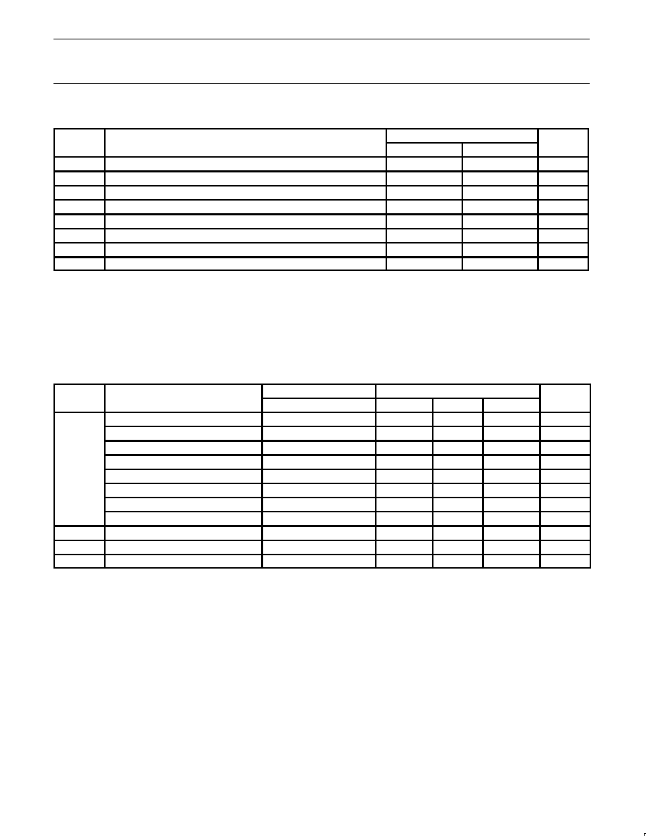
PIN
NO.
PIN NAME
DESCRIPTION
17
LBVCO_IN
Lowband VCO input
18
GND
Ground
19
MXR≠_OUT
Mixer negative output
20
MXR+_OUT
Mixer positive output
21
GND
Ground
22
LBMXR_IN
Lowband mixer input
23
V
CC
Power supply
24
GND
Ground
25
LBLNA_IN
Lowband LNA input
26
GND
Ground
27
GND
Ground
28
LBLNA_OUT
Lowband LNA output
¡¡¡
¡¡¡
29
¡¡¡¡¡¡
¡¡¡¡¡¡
GND
¡¡¡¡¡¡¡¡¡¡
¡¡¡¡¡¡¡¡¡¡
Ground
¡¡¡
¡¡¡
30
¡¡¡¡¡¡
¡¡¡¡¡¡
HBLNA_OUT
¡¡¡¡¡¡¡¡¡¡
¡¡¡¡¡¡¡¡¡¡
Highband LNA output
¡¡¡
¡¡¡
31
¡¡¡¡¡¡
¡¡¡¡¡¡
GND
¡¡¡¡¡¡¡¡¡¡
¡¡¡¡¡¡¡¡¡¡
Ground
¡¡¡
¡¡¡
32
¡¡¡¡¡¡
¡¡¡¡¡¡
GND
¡¡¡¡¡¡¡¡¡¡
¡¡¡¡¡¡¡¡¡¡
Ground
BLOCK DIAGRAM
2
3
4
5
6
7
8
TOP VIEW
1
9
10
11
12
13
14
15
16
17
18
19
20
21
22
23
24
25
26
27
28
29
30
31
32
HBLNA_IN
GND
HBMXR+_IN
HBMXR≠_IN
PD1
GND
PD2
GND
GND
LBVCO_OUT
GND
HBVCO_IN
PD3
GND
LBLNA_IN
GND
LBMXR_IN
GND
MXR+_OUT
MXR≠_OUT
GND
LBVCO_IN
GND
GND
HBLNA_OUT
GND
LBLNA_OUT
GND
GND
V
CC
V
CC
V
CC
SR02238
x2
Figure 1.
Block Diagram
Philips Semiconductors
Preliminary specification
SA3601
Low voltage dual-band RF front-end
1999 Nov 09
4
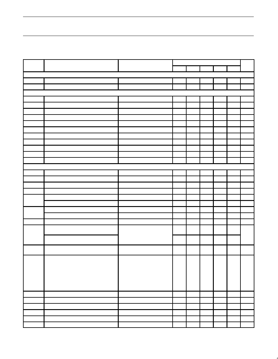
MODE SELECT LOGIC
PD1
PD2
PD3
OPERATING MODE
Cel
LNA
Cel
MXR
PCS
LNA
PCS
MXR
x2
DBL
LB LO
O/P
HB LO
O/P
0
0
0
Sleep mode
off
off
off
off
off
off
off
0
0
1
Tx mode, LO lowband buffer
off
off
off
off
off
on
off
0
1
0
Rx mode cellular, low gain
off
on
off
off
off
on
off
0
1
1
Rx mode cellular, high gain
on
on
off
off
off
on
off
1
0
0
Rx mode PCS, low gain, x2
off
off
off
on
on
on
off
1
0
1
Rx mode PCS, high gain, x2
off
off
on
on
on
on
off
1
1
0
Rx mode PCS, low gain, no x2
off
off
off
on
off
off
off
1
1
1
Rx mode PCS, high gain, no x2
off
off
on
on
off
off
off

Philips Semiconductors
Preliminary specification
SA3601
Low voltage dual-band RF front-end
1999 Nov 09
5
OPERATION
The SA3601 is a highly integrated dual-band radio frequency (RF)
front-end integrated circuit (IC) targeted for TDMA applications. This
IC is split into separate low-band (LB) and high-band (HB) receivers.
The LB receiver contains a low noise amplifier (LNA) and mixer that
are designed to operate in the cellular frequency range
(869≠894MHz). The HB receiver contains an LNA and mixer that
are designed to operate in the PCS frequency range
(1930≠1990 MHz). The SA3601 also contains a frequency doubler
that can drive the HB mixer local oscillator (LO) port, allowing a
single-band voltage controlled oscillator (VCO) to be used to drive
both mixers. Modes for bypassing the doubler are also provided, in
the case where a dual-band VCO is used.
The SA3601 has eight modes of operation that control the LNAs,
mixers, LO buffers and doubler. The select pins (PD1,2,3) are used
to change modes of operation. The internal select logic powers the
device down (0,0,0), turns on the LB LO buffer for use in transmit
mode (0,0,1), enables cellular receive mode for high and low gain
(0,1,X), enables PCS receive mode for high and low gain both
without doubler (1,1,X) and with doubler (1,0,X).
Low-Band Receive Section
The LB circuit contains a LNA followed by a wide dynamic range
active mixer. In a typical application circuit, the LNA output uses an
external pull-up inductor to VCC and is AC coupled. The mixer IF
outputs are differential and are combined with the high-band IF
mixer outputs thereby eliminating the need for extra output pins.
External inductors and capacitors can be used to convert the
differential mixer outputs to single-ended. Furthermore, the LNA
provides two gain settings: high gain (17dB) and low gain (≠15 dB).
The desired gain state can be selected by setting the logic pins
(PD1,PD2,PD3) appropriately.
High-Band Receive Section
The HB circuit contains a LNA followed by a Gilbert cell mixer with
differential inputs. The LNA output uses an internal pull-up inductor
to VCC , which eliminates the need for an external pull-up. The
mixer IF outputs are differential and are combined with the low-band
IF mixer outputs thereby eliminating the need for extra output pins.
Similar to the LB LNA, the HB LNA has two gain settings: high gain
(16 dB) and low gain (≠15 dB).
Control Logic Section
Pins PD1, PD2, and PD3, control the logic functions of the SA3601.
The PD1 selects between LB and HB operations. In LB receive
mode, the LB LNA is in high gain mode (or on) when PD1,2,3 are
(0,1,1). In all other modes, the LB LNA is off. The LB mixer is on
when PD1,2,3 are (0,1,X). In all other modes, the LB mixer is off.
During transmit mode when PD1,2,3 are (0,0,1), the LB LO buffer is
on, enabling use of the LO signal for the transmitter.
In HB receive mode, the HB LNA is in high gain mode (or on) when
PD1,2,3 are (1,X,1). In all other modes, the HB LNA is off. The HB
mixer is on when PD1,2,3 are (1,X,X), and is off in all other modes.
The on-chip frequency doubler (X2) is on in (1,0,X) modes. When
the frequency doubler is on, the input signal from the LB LO buffer is
doubled in frequency, which can then be used to drive the HB mixer
LO port. The frequency doubler can also be bypassed in modes
(1,1,X), in which case the HB mixer is driven directly by an external
2 GHz LO signal.
Philips Semiconductors
Preliminary specification
SA3601
Low voltage dual-band RF front-end
1999 Nov 09
6
ABSOLUTE MAXIMUM RATINGS
1
SYMBOL
PARAMETER
LIMITS
UNITS
SYMBOL
PARAMETER
MIN.
MAX.
UNITS
V
CC
Supply voltage
≠0.3
+4.5
V
V
IN
Voltage applied to any other pin
≠0.3
V
CC
+0.3
V
P
D
Power dissipation, T
amb
= +25
∞
C (still air)
TBD
mW
T
J MAX
Maximum junction temperature
150
∞
C
P
MAX
Power input/output
+20
dBm
I
MAX
DC current into any I/O pin
≠10
+10
mA
T
STG
Storage temperature range
≠65
+150
∞
C
T
O
Operating temperature
≠40
+85
∞
C
NOTES:
1. IC is protected for ESD voltages up to 500 V (human body model).
DC ELECTRICAL CHARACTERISTICS
Unless otherwise specified, all Input/Output ports are single-ended.
DC PARAMETERS
V
CC
= +3.0 V, T
amb
= +25
∞
C; unless otherwise specified
SYMBOL
PARAMETER
TEST CONDITIONS
TESTER LIMITS
UNIT
SYMBOL
PARAMETER
PD1
PD2
PD3
MIN
TYP
MAX
UNIT
Sleep mode
0
0
0
0.1
1
µ
A
Tx mode, LO lowband buffer
0
0
1
4.3
5.5
mA
Rx mode cellular, low gain
0
1
0
10.1
12
mA
I
CC
Rx mode cellular, high gain
0
1
1
14
16.5
mA
I
CC
Rx mode PCS, low gain, x2
1
0
0
17.5
21
mA
Rx mode PCS, high gain, x2
1
0
1
23.5
28
mA
Rx mode PCS, low gain, no x2
1
1
0
10
TBD
mA
Rx mode PCS, high gain, no x2
1
1
1
15.5
TBD
mA
V
IH
Input HIGH voltage
0.5xV
CC
V
CC
+0.3
V
V
IL
Input LOW voltage
≠0.3
0.2xV
CC
V
I
BIAS
Input bias current
Logic 1 or logic 0
≠5
+5
µ
A

Philips Semiconductors
Preliminary specification
SA3601
Low voltage dual-band RF front-end
1999 Nov 09
7
AC ELECTRICAL CHARACTERISTICS
V
CC
= +3.0 V, f
RF
= 881 MHz, f
LO
= 963 MHz, T
amb
= +25
∞
C, unless otherwise specified
SYMBOL
PARAMETER
TEST CONDITIONS
LIMITS
UNIT
SYMBOL
PARAMETER
TEST CONDITIONS
MIN.
≠3
TYP
+3
MAX.
UNIT
Cascaded Gain Section
G
SYS
LB LNA + Mixer, High Gain
Filter loss = 3 dB
20.5
23.5
26.5
dB
G
BYP
LB LNA + Mixer, Low Gain
Filter loss = 3 dB
≠11.5
≠8.5
≠5.5
dB
Low-band LNA Section
f
RF
RF input frequency range
869
894
MHz
G
ENA
Small signal gain ENABLED
17
dB
NF
ENA
Noise figure ENABLED
1.7
dB
IIP3
ENA
Input 3rd order Intercept Point
≠7
dBm
P1dB
ENA
Input 1 dB Compression Point
≠20
dBm
G
BYP
Small signal gain BYPASSED
≠15
dB
NF
BYP
Noise figure BYPASSED
15
dB
IIP3
BYP
Input 3rd order Intercept Point
15
dBm
Z
IN
Input return loss
50
system
10
dB
Z
OUT
Output return loss
50
system
10
dB
T
SW
ENABLE/DISABLE speed
1
20
µ
s
Low-band Mixer Section
f
RF
RF input frequency range
869
894
MHz
f
IF
IF output frequency range
70
200
MHz
f
LO
LO input range
939
1100
MHz
G
MXR
Small signal gain
P
LO
= ≠5 dBm
9.5
dB
NF
MXR
SSB Noise figure
P
LO
= ≠5 dBm
9.5
dB
IIP3
MXR
Input 3rd order Intercept Point
P
LO
= ≠5 dBm
6
dBm
P1dB
MXR
Input 1 dB Compression Point
P
LO
= ≠5 dBm
≠14
dBm
P
LO
LO input power range
≠7
≠5
≠3
dBm
Z
IN
Input return loss
50
system
10
dB
Z
OUT
Output return loss
50
system
10
dB
Two-tone spurious rejection:
P
LO
= ≠5 dBm
2-Tone
2(f
RF
≠f
Tx
), f
RF
≠f
Tx
=f
IF
/2
f
RF
=890.0 MHz @≠36 dBm
f
Tx
=848.9 MHz @≠20 dBm
≠110
dBm
3(f
RF
≠f
Tx
), f
RF
≠f
Tx
=f
IF
/3
f
RF
=876.3 MHz @≠36 dBm
f
Tx
=848.9 MHz @≠20 dBm
≠110
RF≠LO
RF to LO isolation
25
dB
LO≠RF
LO to RF isolation
40
dB
T
SW
ENABLE/DISABLE speed
1
20
µ
s
Low-band LO Buffer Section
P
LO
LO Input frequency range
939
1100
MHz
P
IN
LO Input power
50
matched LB_VCO_IN
≠7
≠5
≠3
dBm
P
OUT
LO Output power
50
matched LB_VCO_OUT
≠7.5
dBm
Z
IN
Input return loss
50
system
10
dB
Z
OUT
Output return loss
50
system
10
dB
Harmonic content
P
LO
= ≠5 dBm
≠20
dBc
T
SW
ENABLE/DISABLE speed
1
20
µ
s
Philips Semiconductors
Preliminary specification
SA3601
Low voltage dual-band RF front-end
1999 Nov 09
8
AC ELECTRICAL CHARACTERISTICS
V
CC
= +3.0 V, f
RF
= 1960 MHz, f
LO
= 2042 MHz, T
amb
= +25
∞
C, unless otherwise specified
SYMBOL
PARAMETER
TEST CONDITIONS
LIMITS
UNIT
SYMBOL
PARAMETER
TEST CONDITIONS
MIN.
≠3
TYP
+3
MAX.
UNIT
Cascaded Gain Section
G
SYS
HB LNA + Mixer, High Gain
Filter loss = 3 dB
18.5
21.5
24.5
dB
G
BYP
HB LNA + Mixer, Low Gain
Filter loss = 3 dB
≠12.5
≠9.5
≠6.5
dB
High-band LNA Section
f
RF
RF input frequency range
1930
1990
MHz
G
ENA
Small signal gain ENABLED
16
dB
NF
ENA
Noise figure ENABLED
2.2
dB
IIP3
ENA
Input 3rd order Intercept Point
≠5
dBm
P1dB
ENA
Input 1 dB Compression Point
≠14
dBm
G
BYP
Small signal gain BYPASSED
≠15
dB
NF
BYP
Noise figure BYPASSED
15
dB
IIP3
BYP
Input 3rd order Intercept Point
15
dBm
Z
IN
Input return loss
50
system, ENA and BYP
10
dB
Z
OUT
Output return loss
50
system, ENA and BYP
10
dB
T
SW
ENABLE/DISABLE speed
1
20
µ
s
High-band Mixer Section
f
RF
RF input frequency range
1930
1990
MHz
f
IF
IF output frequency range
70
200
MHz
f
LO
LO input range
2000
2190
MHz
G
MXR
Small signal gain
P
LO
= ≠5 dBm
8.5
dB
NF
SSB Noise figure, doubler off
P
LO
= ≠5 dBm
8.5
dB
NF
MXR
SSB Noise figure, doubler on
P
LO
= ≠5 dBm
9
dB
IIP3
Input 3rd order Intercept Point, doubler off
P
LO
= ≠5 dBm
5.5
dBm
IIP3
MXR
Input 3rd order Intercept Point, doubler on
P
LO
= ≠5 dBm
3
dBm
P1dB
MXR
Input 1 dB Compression Point
P
LO
= ≠5 dBm
≠14
dBm
IF/2 rej
Half-IF spurious rejection
2(f
RF
≠f
LO
), f
RF
≠f
LO
=f
IF
/2, doubler off
f
RF
=1972.0 MHz @≠36 dBm
≠90
dBm
IF/2 rej.
Half-IF spurious rejection
2(f
RF
≠f
LO
), f
RF
≠f
LO
=f
IF
/2, doubler on
RF
f
LO
=2013.1 MHz @≠5 dBm
≠85
dBm
IF/3 rej.
Third-IF spurious rejection
3(f
RF
≠f
LO
), f
RF
≠f
LO
=f
IF
/3
f
RF
=1985.7 MHz @≠36 dBm
f
LO
=2013.1 MHz @≠5 dBm
≠114
dBm
Two-tone spurious rejection:
P
LO
= ≠5 dBm,
f
RF
≠f
Tx
, f
RF
≠f
Tx
=f
IF
f
RF
=1933.0 MHz @≠36 dBm
f
Tx
=1850.8 MHz @≠20 dBm
≠70
2-Tone
2(f
RF
≠f
Tx
), f
RF
≠f
Tx
=f
IF
/2
f
RF
=1951.0 MHz @≠36 dBm
f
Tx
=1909.9 MHz @≠20 dBm
≠115
dBm
3(f
RF
≠f
Tx
), f
RF
≠f
Tx
=f
IF
/3
f
RF
=1937.3 MHz @≠36 dBm
f
Tx
=1909.9 MHz @≠20 dBm
≠125
P
LO
LO input power range
≠7
≠5
≠3
dBm
Z
IN
Input return loss
50
system
10
dB
Z
OUT
Output return loss
50
system
10
dB
RF≠LO
RF to LO isolation
40
dB
LO≠RF
LO to RF isolation
30
dB
T
SW
ENABLE/DISABLE speed
1
20
µ
s
Philips Semiconductors
Preliminary specification
SA3601
Low voltage dual-band RF front-end
1999 Nov 09
9
AC ELECTRICAL CHARACTERISTICS
V
CC
= +3.0 V, T
amb
= +25
∞
C, unless otherwise specified
SYMBOL
PARAMETER
TEST CONDITIONS
LIMITS
UNITS
SYMBOL
PARAMETER
TEST CONDITIONS
MIN.
≠3
TYP
+3
MAX.
UNITS
High-band LO Buffer Section
P
LO
LO Input frequency range
2000
2190
MHz
P
IN
LO Input power
50
matched HB_VCO_IN
≠7
≠5
≠3
dBm
P
OUT
LO Output power
50
matched HB_VCO_OUT
≠8
dBm
Z
IN
Input return loss
50
system
10
dB
Z
OUT
Output return loss
50
system
10
dB
Harmonic content
P
LO
= ≠5 dBm
≠20
dBc
T
SW
ENABLE/DISABLE speed
1
20
µ
s
x2 LO Doubler Section
f
LO
LO Input frequency
1000
1095
MHz
P
IN
LO Input power
50
matched LB_VCO_IN
≠7
≠5
≠3
dBm
Z
IN
Input return loss
50
system
10
dB
Z
OUT
Output return loss
50
system
10
dB
T
SW
ENABLE/DISABLE speed
1
20
µ
s
NOTES:
1. Dependent on external components.
Philips Semiconductors
Preliminary specification
SA3601
Low voltage dual-band RF front-end
1999 Nov 09
10
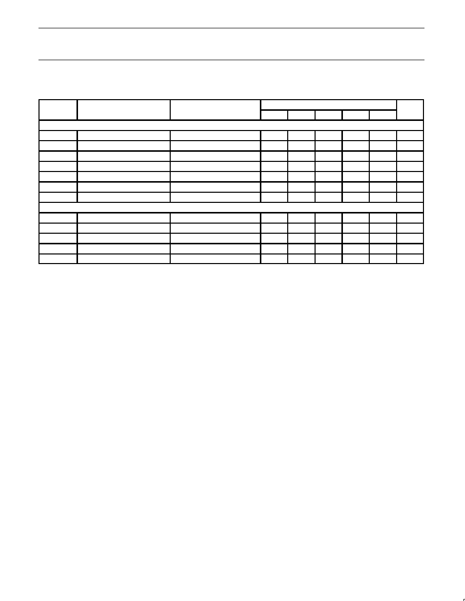
PIN NO
PIN MNEMONIC
DC V
EQUIVALENT CIRCUIT
1
HB LNA IN
0.8
SR01787
V
BIAS
5K
3, 7, 23
V
CC
V
CC
V
BIAS
4
HB MXR+ IN
1.2
5
HB MXR≠ IN
1.2
SR01788
6
PD1
9
PD2
Apply externally
15
PD3
SR01789
12
LB VCO OUT
V
CC
≠ 0.2 V
SR01791
V
CC
14
HB VCO IN
1.9
SR01792
V
BIAS
V
BIAS
V
CC

Philips Semiconductors
Preliminary specification
SA3601
Low voltage dual-band RF front-end
1999 Nov 09
11
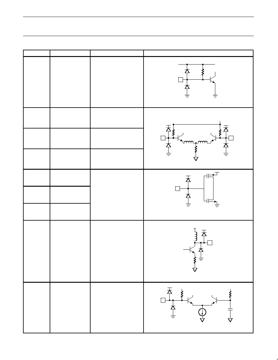
PIN NO
EQUIVALENT CIRCUIT
DC V
PIN MNEMONIC
17
LB VCO IN
1.0
SR01793
V
CC
19
MXR≠ OUT
Pull-up externally to V
CC
2 pF
V
CC
V
CC
20
MXR+ OUT
Pull-u externally to V
CC
SR01794
2 pF
22
LB MXR IN
1.2
SR01795
V
BIAS
V
CC
25
LB LNA IN
0.8
SR01796
V
BIAS
5K
V
CC
Philips Semiconductors
Preliminary specification
SA3601
Low voltage dual-band RF front-end
1999 Nov 09
12
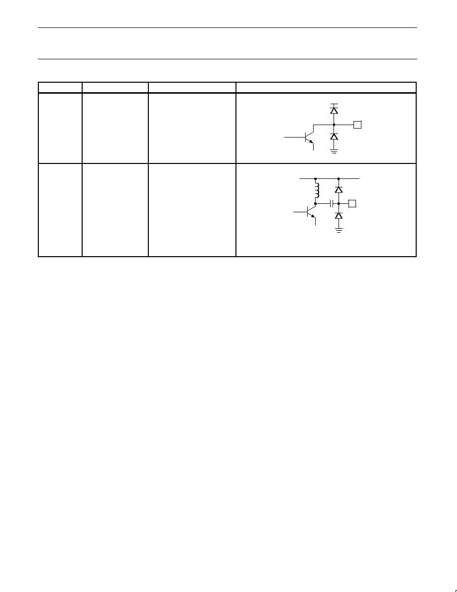
PIN NO
EQUIVALENT CIRCUIT
DC V
PIN MNEMONIC
28
LB LNA OUT
Pull-up externally to V
CC
SR01797
V
CC
30
HB LNA OUT
SR01786
V
CC

Philips Semiconductors
Preliminary specification
SA3601
Low voltage dual-band RF front-end
1999 Nov 09
13
HBCC32:
plastic, heatsink bottom chip carrier; 32 terminals; body 5 x 5 x 0.65 mm
SOT560-1

Philips Semiconductors
Preliminary specification
SA3601
Low voltage dual-band RF front-end
1999 Nov 09
14
Definitions
Short-form specification -- The data in a short-form specification is extracted from a full data sheet with the same type number and title. For
detailed information see the relevant data sheet or data handbook.
Limiting values definition -- Limiting values given are in accordance with the Absolute Maximum Rating System (IEC 134). Stress above one
or more of the limiting values may cause permanent damage to the device. These are stress ratings only and operation of the device at these or
at any other conditions above those given in the Characteristics sections of the specification is not implied. Exposure to limiting values for extended
periods may affect device reliability.
Application information -- Applications that are described herein for any of these products are for illustrative purposes only. Philips
Semiconductors make no representation or warranty that such applications will be suitable for the specified use without further testing or
modification.
Disclaimers
Life support -- These products are not designed for use in life support appliances, devices or systems where malfunction of these products can
reasonably be expected to result in personal injury. Philips Semiconductors customers using or selling these products for use in such applications
do so at their own risk and agree to fully indemnify Philips Semiconductors for any damages resulting from such application.
Right to make changes -- Philips Semiconductors reserves the right to make changes, without notice, in the products, including circuits, standard
cells, and/or software, described or contained herein in order to improve design and/or performance. Philips Semiconductors assumes no
responsibility or liability for the use of any of these products, conveys no license or title under any patent, copyright, or mask work right to these
products, and makes no representations or warranties that these products are free from patent, copyright, or mask work right infringement, unless
otherwise specified.
Philips Semiconductors
811 East Arques Avenue
P.O. Box 3409
Sunnyvale, California 94088≠3409
Telephone 800-234-7381
©
Copyright Philips Electronics North America Corporation 2000
All rights reserved. Printed in U.S.A.
Date of release: 04-00
Document order number:
9397 750 07037
Philips
Semiconductors
Data sheet
status
Objective
specification
Preliminary
specification
Product
specification
Product
status
Development
Qualification
Production
Definition
[1]
This data sheet contains the design target or goal specifications for product development.
Specification may change in any manner without notice.
This data sheet contains preliminary data, and supplementary data will be published at a later date.
Philips Semiconductors reserves the right to make changes at any time without notice in order to
improve design and supply the best possible product.
This data sheet contains final specifications. Philips Semiconductors reserves the right to make
changes at any time without notice in order to improve design and supply the best possible product.
Data sheet status
[1]
Please consult the most recently issued datasheet before initiating or completing a design.