 | –≠–ª–µ–∫—Ç—Ä–æ–Ω–Ω—ã–π –∫–æ–º–ø–æ–Ω–µ–Ω—Ç: SA5204AD | –°–∫–∞—á–∞—Ç—å:  PDF PDF  ZIP ZIP |

Philips Semiconductors
NE/SA5204A
Wide-band high-frequency amplifier
Product specification
1992 Feb 25
INTEGRATED CIRCUITS
RF Communications Handbook
Philips Semiconductors
Product specification
NE/SA5204A
Wide-band high-frequency amplifier
2
1992 Feb 25
853-1599 05790
DESCRIPTION
The NE/SA5204A family of wideband amplifiers replaces the
NE/SA5204 family. The `A' parts are fabricated on a rugged 2
µ
m
bipolar process featuring excellent statistical process control.
Electrical performance is nomically identical to the original parts.
The NE/SA5204A is a high-frequency amplifier with a fixed insertion
gain of 20dB. The gain is flat to
±
0.5dB from DC to 200MHz. The
-3dB bandwidth is greater than 350MHz. This performance makes
the amplifier ideal for cable TV applications. The NE/SA5204A
operates with a single supply of 6V, and only draws 25mA of supply
current, which is much less than comparable hybrid parts. The noise
figure is 4.8dB in a 75
system and 6dB in a 50
system.
The NE/SA5204A is a relaxed version of the NE5205. Minimum
guaranteed bandwidth is relaxed to 350MHz and the "S" parameter
Min/Max limits are specified as typicals only.
Until now, most RF or high-frequency designers had to settle for
discrete or hybrid solutions to their amplification problems. Most of
these solutions required trade-offs that the designer had to accept in
order to use high-frequency gain stages. These include high power
consumption, large component count, transformers, large packages
with heat sinks, and high part cost. The NE/SA5204A solves these
problems by incorporating a wideband amplifier on a single
monolithic chip.
The part is well matched to 50 or 75
input and output impedances.
The standing wave ratios in 50 and 75
systems do not exceed 1.5
on either the input or output over the entire DC to 350MHz operating
range.
Since the part is a small, monolithic IC die, problems such as stray
capacitance are minimized. The die size is small enough to fit into a
very cost-effective 8-pin small-outline (SO) package to further
reduce parasitic effects.
No external components are needed other than AC-coupling
capacitors because the NE/SA5204A is internally compensated and
matched to 50 and 75
. The amplifier has very good distortion
specifications, with second and third-order intermodulation
intercepts of +24dBm and +17dBm, respectively, at 100MHz.
The part is well matched for 50
test equipment such as signal
generators, oscilloscopes, frequency counters, and all kinds of
signal analyzers. Other applications at 50
include mobile radio, CB
radio, and data/video transmission in fiber optics, as well as
broadband LANs and telecom systems. A gain greater than 20dB
can be achieved by cascading additional NE/SA5204As in series as
required, without any degradation in amplifier stability.
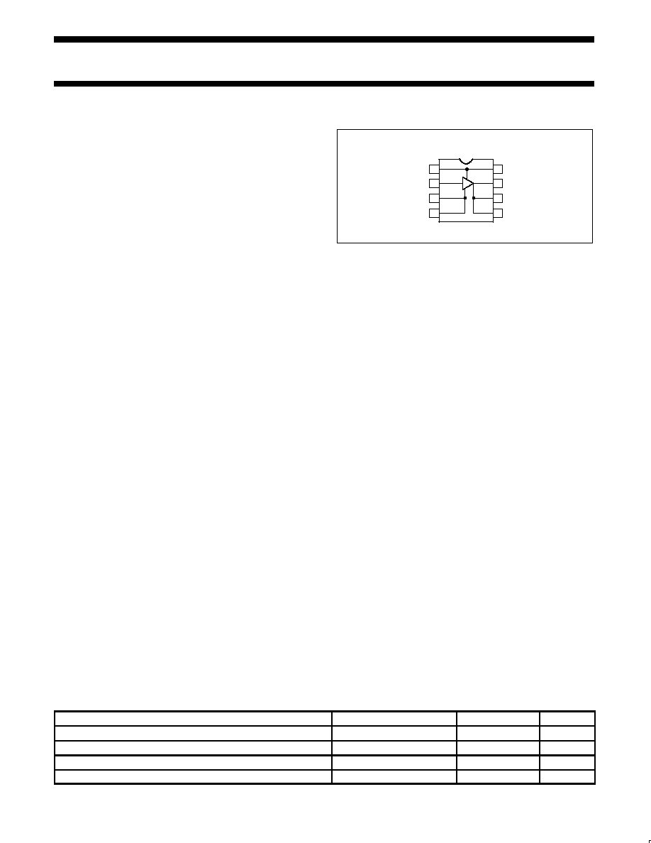
PIN CONFIGURATION
N, D Packages
8
7
6
5
4
3
2
1
VCC
VIN
GND
GND
VCC
VOUT
GND
GND
TOP VIEW
20dB
SR00193
Figure 1. Pin Configuration
FEATURES
∑
Bandwidth (min.)
200 MHz,
±
0.5dB
350 MHz, -3dB
∑
20dB insertion gain
∑
4.8dB (6dB) noise figure Z
O
=75
(Z
O
=50
)
∑
No external components required
∑
Input and output impedances matched to 50/75
systems
∑
Surface-mount package available
∑
Cascadable
∑
2000V ESD protection
APPLICATIONS
∑
Antenna amplifiers
∑
Amplified splitters
∑
Signal generators
∑
Frequency counters
∑
Oscilloscopes
∑
Signal analyzers
∑
Broadband LANs
∑
Networks
∑
Modems
∑
Mobile radio
∑
Security systems
∑
Telecommunications
ORDERING INFORMATION
DESCRIPTION
TEMPERATURE RANGE
ORDER CODE
DWG #
8-Pin Plastic Dual In-Line Package (DIP)
0 to +70
∞
C
NE5204AN
SOT97-1
8-Pin Plastic Small Outline (SO) package
0 to +70
∞
C
NE5204AD
SOT96-1
8-Pin Plastic Dual In-Line Package (DIP)
≠40 to +85
∞
C
SA5204AN
SOT97-1
8-Pin Plastic Small Outline (SO) package
≠40 to +85
∞
C
SA5204AD
SOT96-1
Philips Semiconductors
Product specification
NE/SA5204A
Wide-band high-frequency amplifier
1992 Feb 25
3
ABSOLUTE MAXIMUM RATINGS
SYMBOL
PARAMETER
RATING
UNIT
V
CC
Supply voltage
9
V
V
IN
AC input voltage
5
V
P≠P
T
A
Operating ambient temperature range
NE grade
0 to +70
∞
C
SA grade
≠40 to +85
∞
C
P
DMAX
Maximum power dissipation
1, 2
T
A
=25
∞
C(still≠air)
N package
1160
mW
D package
780
mW
T
J
Junction temperature
150
∞
C
T
STG
Storage temperature range
≠55 to +150
∞
C
T
SOLD
Lead temperature
(soldering 60s)
300
∞
C
NOTES:
1. Derate above 25
∞
C, at the following rates
N package at 9.3mW/
∞
C
D package at 6.2mW/
∞
C
2. See "Power Dissipation Considerations" section.
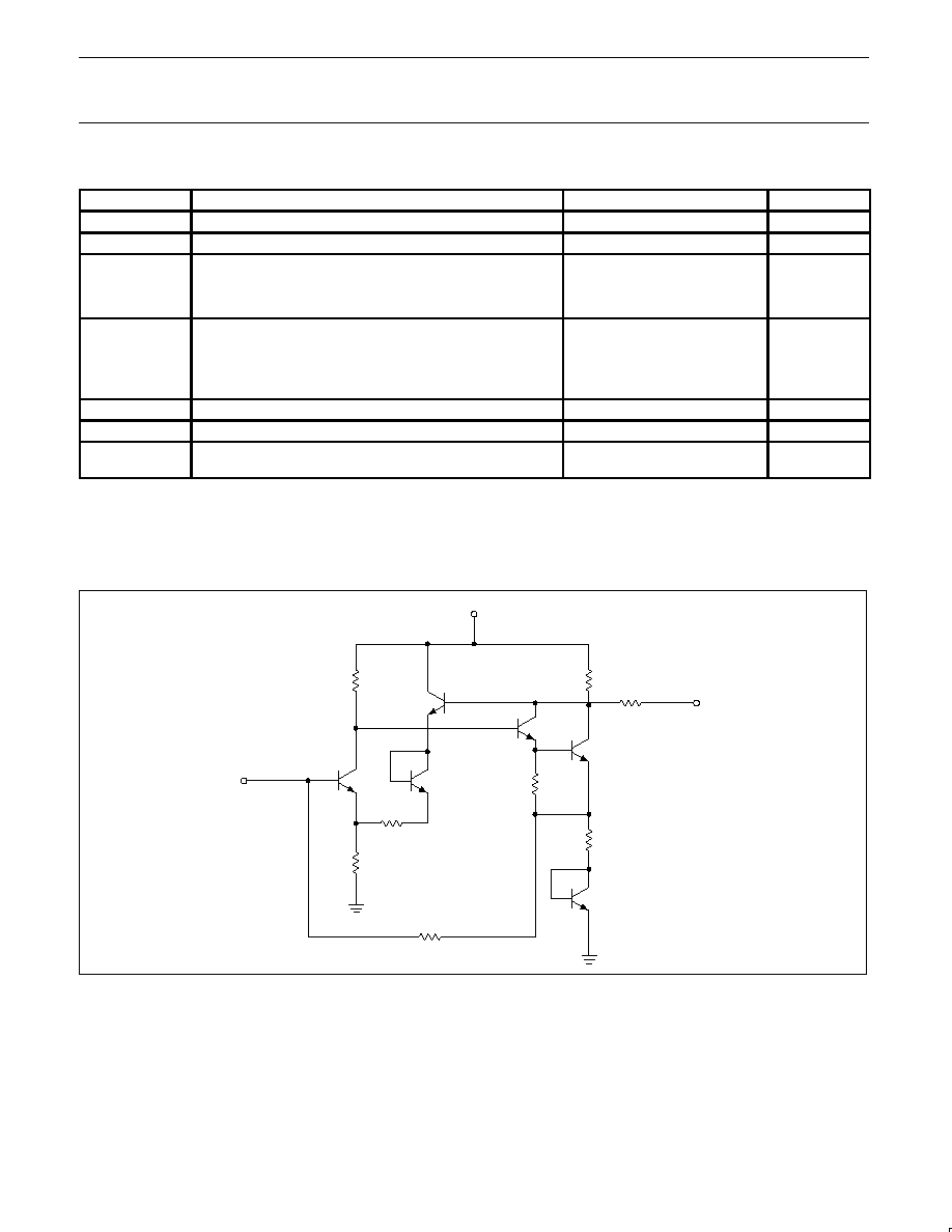
EQUIVALENT SCHEMATIC
VCC
VIN
R1
R2
R0
RF1
RE1
RF2
RE2
R3
Q3
Q4
Q6
Q1
Q2
Q5
VOUT
SR00194
Figure 2. Equivalent Schematic
Philips Semiconductors
Product specification
NE/SA5204A
Wide-band high-frequency amplifier
1992 Feb 25
4
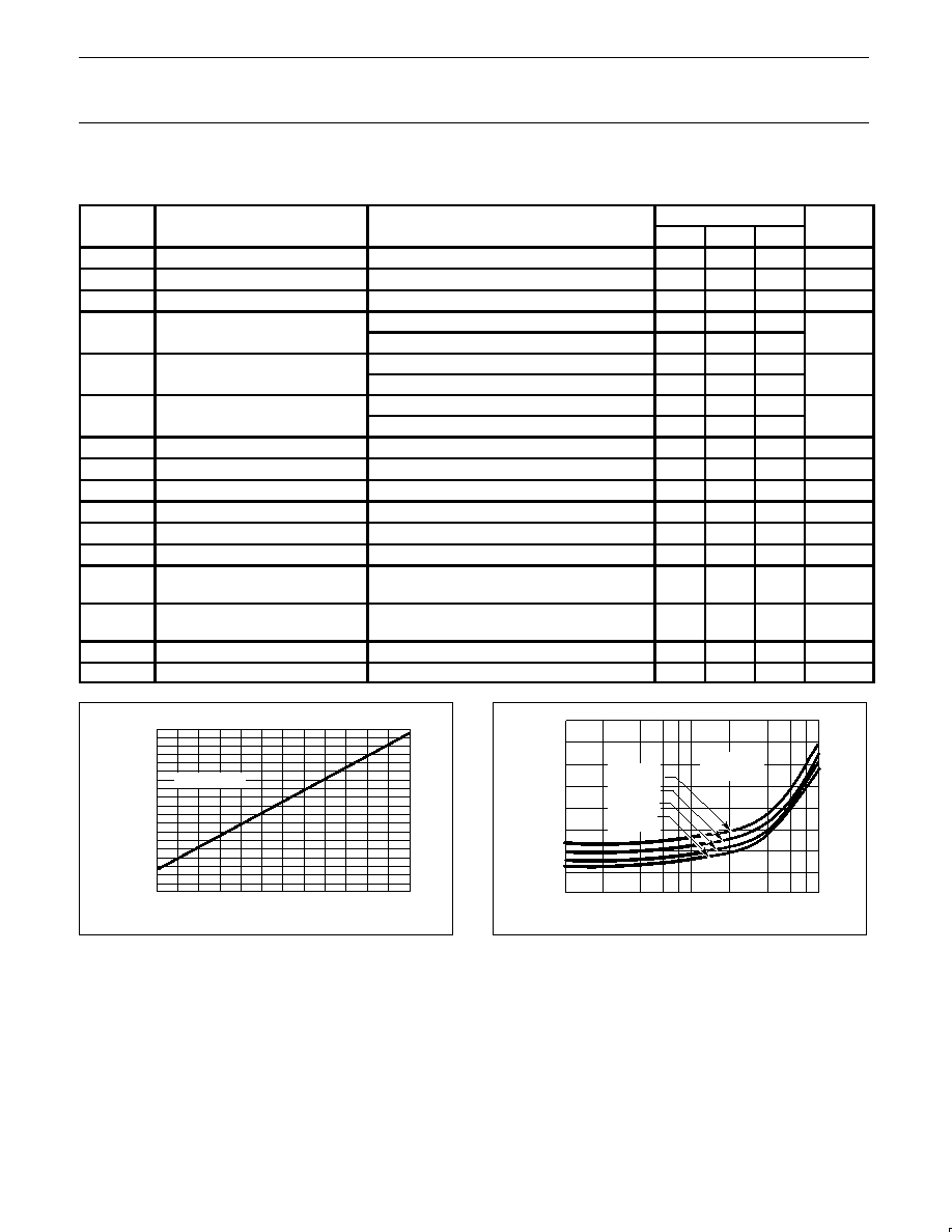
DC ELECTRICAL CHARACTERISTICS
V
CC
=6V, Z
S
=Z
L
=Z
O
=50
and T
A
=25
∞
C, in all packages, unless otherwise specified.
SYMBOL
PARAMETER
TEST CONDITIONS
LIMITS
UNIT
SYMBOL
PARAMETER
TEST CONDITIONS
Min
Typ
Max
UNIT
V
CC
Operating supply voltage range
Over temperature
5
8
V
I
CC
Supply current
Over temperature
19
25
33
mA
S21
Insertion gain
f=100MHz, over temperature
16
19
22
dB
S11
Input return loss
f=100MHz
25
dB
S11
Input return loss
DC ≠550MHz
12
dB
S22
Output return loss
f=100MHz
27
dB
S22
Output return loss
DC ≠550MHz
12
dB
S12
Isolation
f=100MHz
≠25
dB
S12
Isolation
DC ≠550MHz
≠18
dB
BW
Bandwidth
±
0.5dB
200
350
MHz
BW
Bandwidth
≠3dB
350
550
MHz
Noise figure (75
)
f=100MHz
4.8
dB
Noise figure (50
)
f=100MHz
6.0
dB
Saturated output power
f=100MHz
+7.0
dBm
1dB gain compression
f=100MHz
+4.0
dBm
Third≠order intermodulation inter-
cept (output)
f=100MHz
+17
dBm
Second≠order intermodulation inter-
cept (output)
f=100MHz
+24
dBm
t
R
Rise time
500
ps
t
P
Propagation delay
500
ps
SUPPL
Y
CURRENT--mA
35
34
32
30
28
26
24
22
20
18
16
5
5.5
6
6.5
7
7.5
8
SUPPLY VOLTAGE--V
TA = 25
o
C
SR00195
Figure 3. Supply Current vs Supply Voltage
NOISE FIGURE--dBm
vcc = 6v
vcc = 8v
vcc = 7v
vcc = 5v
9
8
7
6
5
ZO = 50
TA = 25
o
C
FREQUENCY--MHz
101
2
4
6
8
2
4
6
8
102
103
SR00196
Figure 4. Noise Figure vs Frequency
Philips Semiconductors
Product specification
NE/SA5204A
Wide-band high-frequency amplifier
1992 Feb 25
5
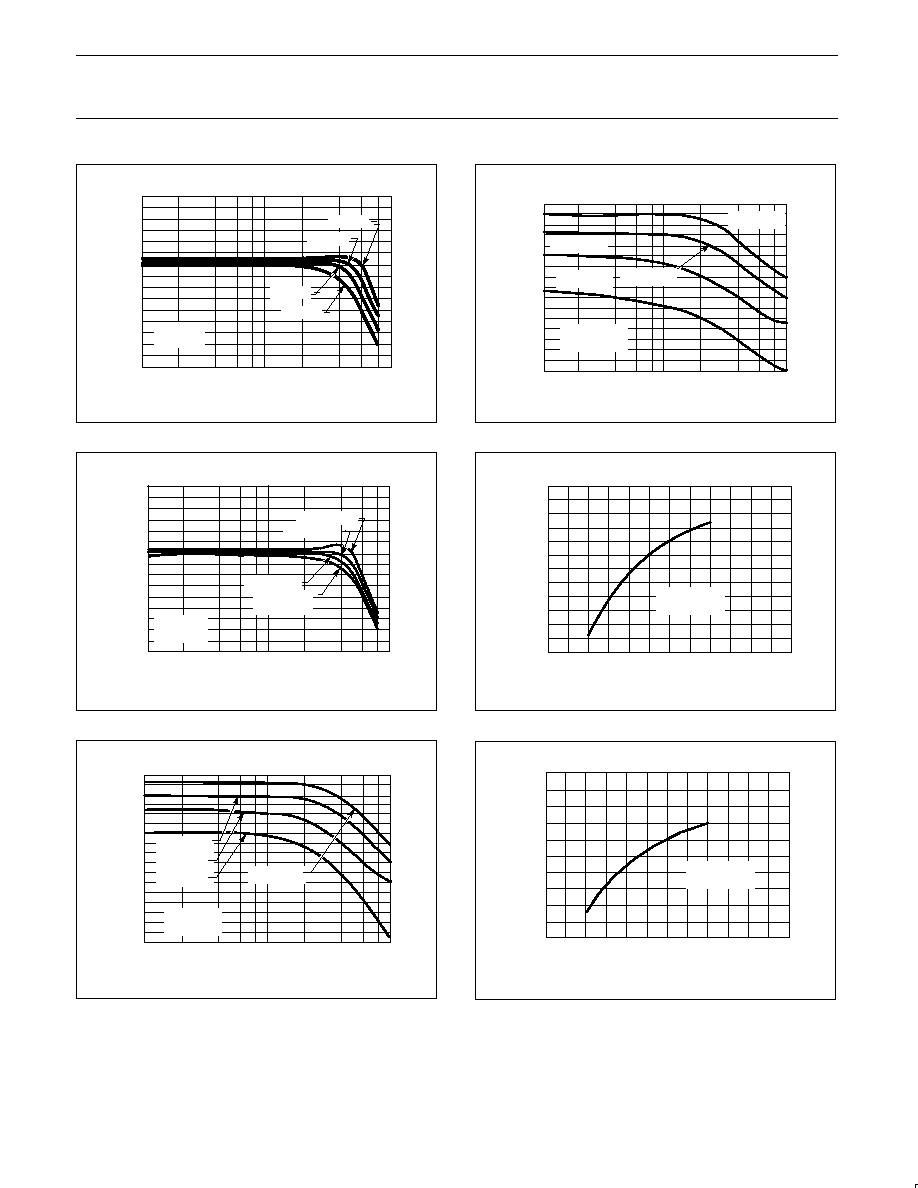
INSERTION GAIN--dB
25
20
15
10
101
2
4
6
8
2
4
6
8
102
103
FREQUENCY--MHz
ZO = 50
TA = 25
o
C
vcc = 5v
vcc = 8v
vcc = 7v
vcc = 6v
SR00197
Figure 5. Insertion Gain vs Frequency (S
21
)
TA = 55
o
C
TA = 25
o
C
TA = 85
o
C
TA =
125
o
C
VCC = 8V
ZO = 50
25
20
15
10
101
2
4
6
8
2
4
6
8
102
103
FREQUENCY--MHz
INSERTION GAIN--dB
SR00199
Figure 6. Insertion Gain vs Frequency (S
21
)
FREQUENCY--MHz
ZO = 50
TA = 25
o
C
VCC = 8V
VCC = 7V
VCC = 6V
VCC = 5V
OUTPUT LEVEL--dBm
2
3
4
5
6
7
8
9
10
11
1
0
≠1
≠2
≠3
≠4
≠5
≠6
101
2
4
6
8
2
4
6
8
102
103
SR00201
Figure 7. Saturated Output Power vs Frequency
OUTPUT LEVEL--dBm
VCC = 8V
VCC = 7V
VCC = 6V
VCC = 5V
ZO = 50
TA = 25
o
C
10
9
8
7
6
5
4
3
2
1
0
≠1
≠2
≠3
≠4
≠5
≠6
FREQUENCY--MHz
101
2
4
6
8
2
4
6
8
102
103
SR00198
Figure 8. 1dB Gain Compression vs Frequency
SECOND≠ORDER INTERCEPT--dBm
40
35
30
25
20
15
10
4
5
6
7
8
9
10
POWER SUPPLY VOLTAGE--V
ZO = 50
TA = 25
o
C
SR00200
Figure 9. Second-Order Output Intercept vs Supply Voltage
THIRD≠ORDER INTERCEPT--dBm
30
25
20
15
10
5
4
5
6
7
8
9
10
POWER SUPPLY VOLTAGE--V
ZO = 50
TA = 25
o
C
SR00202
Figure 10. Third-Order Intercept vs Supply Voltage
Philips Semiconductors
Product specification
NE/SA5204A
Wide-band high-frequency amplifier
1992 Feb 25
6
INPUT VSWR
1.0
1.1
1.2
1.3
1.4
1.5
1.6
1.7
1.8
1.9
2.0
FREQUENCY--MHz
TA = 25
o
C
VCC = 6V
ZO = 75
ZO = 50
.
101
2
4
6 8
2
4
6 8
102
103
SR00203
Figure 11. Input VSWR vs Frequency
INPUT VSWR
1.0
1.1
1.2
1.3
1.4
1.5
1.6
1.7
1.8
1.9
2.0
FREQUENCY--MHz
Tamb = 25
o
C
VCC = 6V
ZO = 75
ZO = 50
101
2
4
6 8
2
4
6
8
102
103
SR00205
Figure 12. Output VSWR vs Frequency
INPUT RETURN LOSS--dB
OUTPUT RETURN LOSS--dB
40
35
30
25
20
15
10
OUTPUT
INPUT
FREQUENCY--MHz
VCC = 6V
ZO = 50
TA = 25
o
C
101
2
4
6 8
2
4
6
8
102
103
SR00207
Figure 13. Input (S
11
) and Output (S
22
) Return Loss
vs Frequency
FREQUENCY--MHz
ISOLA
TION--dB
ZO = 50
TA = 25
o
C
VCC = 6V
10
≠15
≠20
≠25
≠30
101
2
4
6 8
2
4
6
8
102
103
SR00204
Figure 14. Isolation vs Frequency (S
12
)
ISOLA
TION GAIN--dB
15
10
25
20
ZO = 75
TA = 25
o
C
vcc = 8v
vcc = 7v
vcc = 6v
vcc = 5v
FREQUENCY--MHz
101
2
4
6 8
2
4
6
8
102
103
SR00206
Figure 15. Insertion Gain vs Frequency (S
21
)
INSERTION GAIN--dB
25
20
15
10
ZO = 75
VCC = 6V
TA = ≠55
o
C
TA = 25
o
C
TA = 85
o
C
TA =
125
o
C
FREQUENCY--MHz
101
2
4
6
8
2
4
6
8
102
103
SR00208
Figure 16. Insertion Gain vs Frequency (S
21
)
Philips Semiconductors
Product specification
NE/SA5204A
Wide-band high-frequency amplifier
1992 Feb 25
7
THEORY OF OPERATION
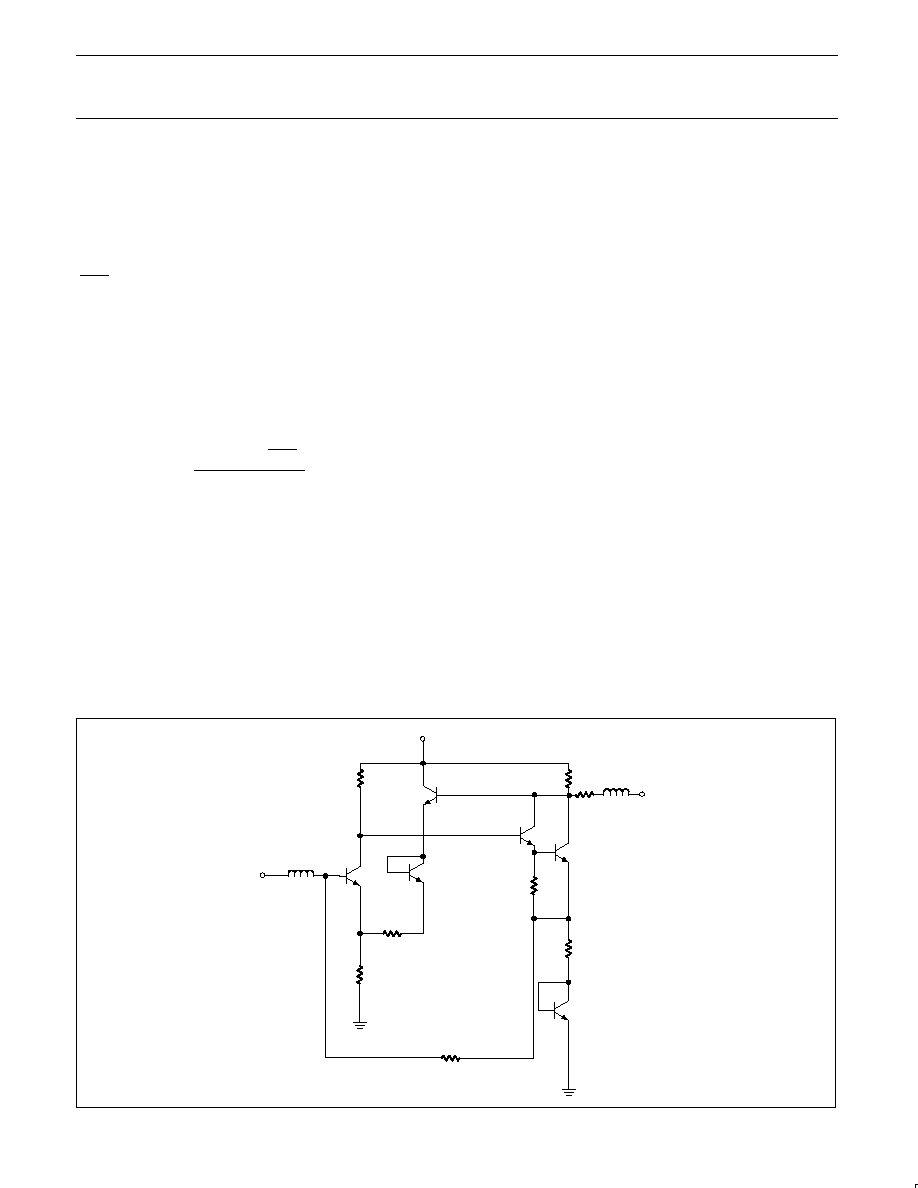
The design is based on the use of multiple feedback loops to
provide wide-band gain together with good noise figure and terminal
impedance matches. Referring to the circuit schematic in Figure 17,
the gain is set primarily by the equation:
V
OUT
V
IN
+
(R
F1
)
R
E1
)
R
E1
(1)
which is series-shunt feedback. There is also shunt-series feedback
due to R
F2
and R
E2
which aids in producing wide-band terminal
impedances without the need for low value input shunting resistors
that would degrade the noise figure. For optimum noise
performance, R
E1
and the base resistance of Q
1
are kept as low as
possible, while R
F2
is maximized.
The noise figure is given by the following equation:
NF
+
10Log
1
)
r
b
)
R
E1
)
KT
2ql
C1
R
O
dB
(2)
where I
C1
=5.5mA, R
E1
=12
, r
b
=130
, KT/q=26mV at 25
∞
C and
R
0
=50 for a 50
system and 75 for a 75
system.
The DC input voltage level V
IN
can be determined by the equation:
V
IN
=V
BE1
+(I
C1
+I
C3
) R
E1
(3)
where R
E1
=12
, V
BE
=0.8V, I
C1
=5mA and I
C3
=7mA (currents rated
at V
CC
=6V).
Under the above conditions, V
IN
is approximately equal to 1V.
Level shifting is achieved by emitter-follower Q
3
and diode Q
4
,
which provide shunt feedback to the emitter of Q
1
via R
F1
. The use
of an emitter-follower buffer in this feedback loop essentially
eliminates problems of shunt-feedback loading on the output. The
value of R
F1
=140
is chosen to give the desired nominal gain. The
DC output voltage V
OUT
can be determined by:
V
OUT
=V
CC
≠(I
C2
+I
C6
)R2,(4)
where V
CC
=6V, R
2
=225
, I
C2
=8mA and I
C6
=5mA.
From here, it can be seen that the output voltage is approximately
3.1V to give relatively equal positive and negative output swings.
Diode Q
5
is included for bias purposes to allow direct coupling of
R
F2
to the base of Q
1
. The dual feedback loops stabilize the DC
operating point of the amplifier.
The output stage is a Darlington pair (Q
6
and Q
2
) which increases
the DC bias voltage on the input stage (Q
1
) to a more desirable
value, and also increases the feedback loop gain. Resistor R
0
optimizes the output VSWR (Voltage Standing Wave Ratio).
Inductors L
1
and L
2
are bondwire and lead inductances which are
roughly 3nH. These improve the high-frequency impedance
matches at input and output by partially resonating with 0.5pF of pad
and package capacitance.
POWER DISSIPATION CONSIDERATIONS
When using the part at elevated temperature, the engineer should
consider the power dissipation capabilities of each package.
At the nominal supply voltage of 6V, the typical supply current is
25mA (32mA max). For operation at supply voltages other than 6V,
see Figure 3 for I
CC
versus V
CC
curves. The supply current is
inversely proportional to temperature and varies no more than 1mA
between 25
∞
C and either temperature extreme. The change is 0.1%
per
∞
C over the range.
The recommended operating temperature ranges are air-mount
specifications. Better heat-sinking benefits can be realized by
mounting the SO and N package bodies against the PC board
plane.
VIN
L1
3nH
Q1
Q4
RF1
140
RE1
12
RF2
200
Q5
RE2
12
R3
140
Q6
10
3nH
L2
VOUT
R2
225
VCC
R1
650
R0
Q3
Q2
SR00209
Figure 17. Schematic Diagram
Philips Semiconductors
Product specification
NE/SA5204A
Wide-band high-frequency amplifier
1992 Feb 25
8
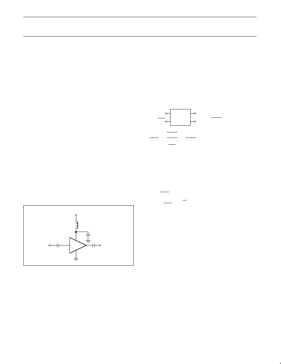
PC BOARD MOUNTING
In order to realize satisfactory mounting of the NE5204A to a PC
board, certain techniques need to be utilized. The board must be
double-sided with copper and all pins must be soldered to their
respective areas (i.e., all GND and V
CC
pins on the package). The
power supply should be decoupled with a capacitor as close to the
V
CC
pins as possible, and an RF choke should be inserted between
the supply and the device. Caution should be exercised in the
connection of input and output pins. Standard microstrip should be
observed wherever possible. There should be no solder bumps or
burrs or any obstructions in the signal path to cause launching
problems. The path should be as straight as possible and lead
lengths as short as possible from the part to the cable connection.
Another important consideration is that the input and output should
be AC-coupled. This is because at V
CC
=6V, the input is
approximately at 1V while the output is at 3.1V. The output must be
decoupled into a low-impedance system, or the DC bias on the
output of the amplifier will be loaded down, causing loss of output
power. The easiest way to decouple the entire amplifier is by
soldering a high-frequency chip capacitor directly to the input and
output pins of the device. This circuit is shown in Figure 18. Follow
these recommendations to get the best frequency response and
noise immunity. The board design is as important as the integrated
circuit design itself.
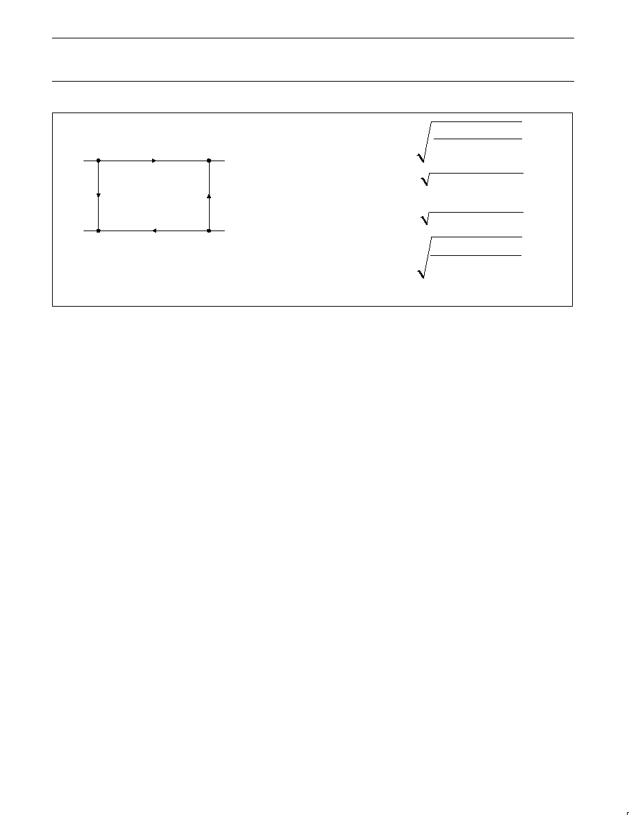
SCATTERING PARAMETERS
The primary specifications for the NE5204A are listed as
S-parameters. S-parameters are measurements of incident and
reflected currents and voltages between the source, amplifier, and
load as well as transmission losses. The parameters for a two-port
network are defined in Figure 19.
NE5204A
VOUT
VIN
VCC
AC
COUPLING
CAPACITOR
RF CHOKE
DECOUPLING
CAPACITOR
AC
COUPLING
CAPACITOR
SR00210
Figure 18. Circuit Schematic for
Coupling and Power Supply Decoupling
Actual S-parameter measurements using an HP network analyzer
(model 8505A) and an HP S-parameter tester (models 8503A/B) are
shown in Figure 20.
Values for the figures below are measured and specified in the data
sheet to ease adaptation and comparison of the NE/SA/SE5204A to
other high-frequency amplifiers.
The most important parameter is S
21
. It is defined as the square root
of the power gain, and, in decibels, is equal to voltage gain as
shown below:
Z
D
=Z
IN
=Z
OUT
for the NE/SA/SE5204A
P
IN
)
V
IN
2
Z
D
P
OUT
)
V
OUT
2
Z
D
N
P
OUT
P
IN
+
V
OUT
2
Z
D
V
IN
2
Z
D
+
V
OUT
2
V
IN
2
+
P
I
NE5204A
Z
D
P
I
=V
I
2
P
I
=Insertion Power Gain
V
I
=Insertion Voltage Gain
Measured value for the
NE/SA/SE5204A = |S
21
|
2
= 100
N
P
I
+
P
OUT
P
IN
+
| S
21
|
2
+
100
and V
I
+
V
OUT
V
IN
+
P
I
+
S
21
+
10
In decibels:
P
I(dB)
=10 Log | S
21
|
2
= 20dB
V
I(dB)
= 20 Log S
21
= 20dB
P
I(dB)
= V
I(dB)
= S
21(dB)
= 20dB
Also measured on the same system are the respective voltage
standing wave ratios. These are shown in Figure 21. The VSWR
can be seen to be below 1.5 across the entire operational frequency
range.
Relationships exist between the input and output return losses and
the voltage standing wave ratios. These relationships are as follows:
Philips Semiconductors
Product specification
NE/SA5204A
Wide-band high-frequency amplifier
1992 Feb 25
9
POWER REFLECTED
FROM OUTPUT PORT
POWER AVAILABLE FROM
GENERATOR AT OUTPUT PORT
S
22
=
POWER AVAILABLE FROM
GENERATOR AT INPUT PORT
REVERSE TRANSDUCER
POWER GAIN
S12 =
S11 -- INPUT RETURN LOSS
a. Two-Port Network Defined
b.
S21
S12
S22
S11
POWER REFLECTED
FROM INPUT PORT
S11 =
S12 -- REVERSE TRANSMISSION LOSS
OSOLATION
S21 -- FORWARD TRANSMISSION LOSS
OR INSERTION GAIN
S21
= TRANSDUCER POWER GAIN
S22
-- OUTPUT RETURN LOSS
SR00211
Figure 19.
Philips Semiconductors
Product specification
NE/SA5204A
Wide-band high-frequency amplifier
1992 Feb 25
10
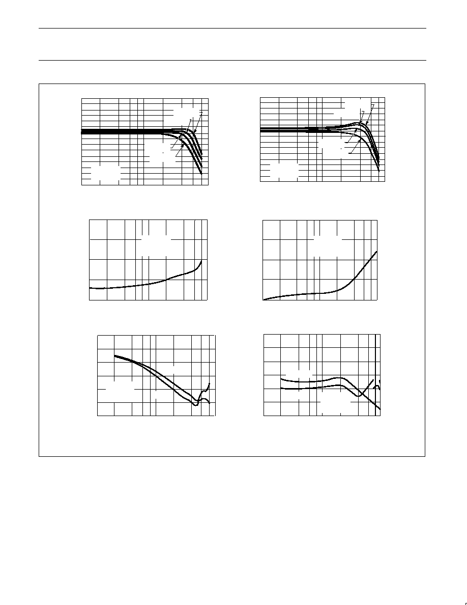
INSERTION GAIN--dB
25
20
15
10
101
2
4
6
8
2
4
6
8
102
103
vcc = 8v
vcc = 7v
vcc = 6v
vcc = 5v
FREQUENCY--MHz
50
System
75
System
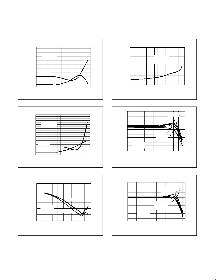
a. Insertion Gain vs Frequency (S
21
)
b. Insertion Gain vs Frequency (S
21
)
c. Isolation vs Frequency (S
12
)
d. S
12
Isolation vs Frequency
e. Input (S
11
) and Output (S
22
) Return Loss
vs Frequency
f. Input (S
11
) and Output (S
22
) Return Loss
vs Frequency
ISOLA
TION GAIN--dB
15
10
25
20
ZO = 75
TA = 25
o
C
vcc = 8v
vcc = 7v
vcc = 6v
vcc = 5v
FREQUENCY--MHz
ZO = 50
TA = 25
o
C
ISOLA
TION--dB
FREQUENCY--MHz
ZO = 50
TA = 25
o
C
VCC = 6V
10
≠15
≠20
≠25
≠30
INPUT RETURN LOSS--dB
OUTPUT RETURN LOSS--dB
40
35
30
25
20
15
10
INPUT
FREQUENCY--MHz
VCC = 6V
ZO = 50
TA = 25
o
C
ZO = 75
TA = 25
o
C
VCC = 6V
ISOLA
TION--dB
10
≠15
≠20
≠25
≠30
FREQUENCY--MHz
VCC = 6V
ZO = 75
TA = 25
o
C
OUTPUT
INPUT
INPUT RETURN LOSS--dB
OUTPUT RETURN LOSS--dB
40
35
30
25
20
15
10
FREQUENCY--MHz
OUTPUT
101
2
4
6
8
2
4
6
8
102
103
101
2
4
6
8
2
4
6 8
102
103
101
2
4
6
8
2
4
6 8
102
103
101
2
4
6
8
2
4
6 8
102
103
101
2
4
6
8
2
4
6 8
102
103
SR00212
Figure 20.
INPUT RETURN LOSS=S
11
dB
S
11
dB=20 Log | S
11
|
OUTPUT RETURN LOSS=S
22
dB
S
22
dB=20 Log | S
22
|
INPUT VSWR=
1.5
OUTPUT VSWR=
1.5
1DB GAIN COMPRESSION AND SATURATED
OUTPUT POWER
The 1dB gain compression is a measurement of the output power
level where the small-signal insertion gain magnitude decreases
1dB from its low power value. The decrease is due to nonlinearities
in the amplifier, an indication of the point of transition between
small-signal operation and the large signal mode.
The saturated output power is a measure of the amplifier's ability to
deliver power into an external load. It is the value of the amplifier's
output power when the input is heavily overdriven. This includes the
sum of the power in all harmonics.
INTERMODULATION INTERCEPT TESTS
The intermodulation intercept is an expression of the low level
linearity of the amplifier. The intermodulation ratio is the difference in
dB between the fundamental output signal level and the generated
distortion product level. The relationship between intercept and
Philips Semiconductors
Product specification
NE/SA5204A
Wide-band high-frequency amplifier
1992 Feb 25
11
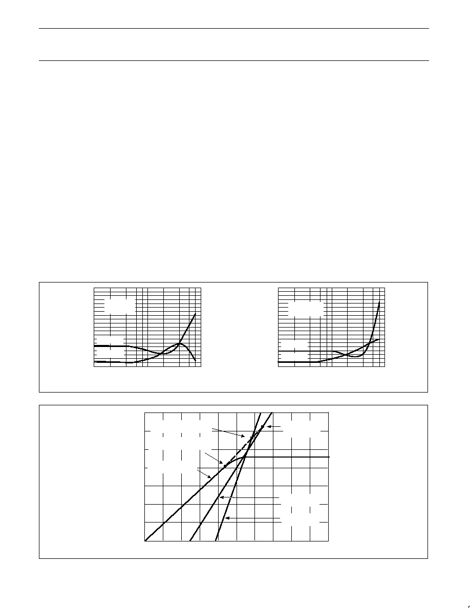
intermodulation ratio is illustrated in Figure 22, which shows product
output levels plotted versus the level of the fundamental output for
two equal strength output signals at different frequencies. The upper
line shows the fundamental output plotted against itself with a 1dB to
1dB slope. The second and third order products lie below the
fundamentals and exhibit a 2:1 and 3:1 slope, respectively.
The intercept point for either product is the intersection of the
extensions of the product curve with the fundamental output.
The intercept point is determined by measuring the intermodulation
ratio at a single output level and projecting along the appropriate
product slope to the point of intersection with the fundamental.
When the intercept point is known, the intermodulation ratio can be
determined by the reverse process. The second order IMR is equal
to the difference between the second order intercept and the
fundamental output level. The third order IMR is equal to twice the
difference between the third order intercept and the fundamental
output level. These are expressed as:
IP
2
=P
OUT
+IMR
2
IP
3
=P
OUT
+IMR
3
/2
where P
OUT
is the power level in dBm of each of a pair of equal
level fundamental output signals, IP
2
and IP
3
are the second and
third order output intercepts in dBm, and IMR
2
and IMR
3
are the
second and third order intermodulation ratios in dB. The
intermodulation intercept is an indicator of intermodulation
performance only in the small signal operating range of the amplifier.
Above some output level which is below the 1dB compression point,
the active device moves into large-signal operation. At this point the
intermodulation products no longer follow the straight line output
slopes, and the intercept description is no longer valid. It is therefore
important to measure IP
2
and IP
3
at output levels well below 1dB
compression. One must be careful, however, not to select too low
levels because the test equipment may not be able to recover the
signal from the noise. For the NE/SA5204A we have chosen an
output level of ≠10.5dBm with fundamental frequencies of 100.000
and 100.01MHz, respectively.
ADDITIONAL READING ON SCATTERING
PARAMETERS
For more information regarding S-parameters, please refer to
High-Frequency Amplifiers by Ralph S. Carson of the University of
Missouri, Rolla, Copyright 1985; published by John Wiley & Sons,
Inc.
"S-Parameter Techniques for Faster, More Accurate Network Design",
HP App Note 95-1, Richard W. Anderson, 1967, HP Journal.
"S-Parameter Design", HP App Note 154, 1972.
a. Input VSWR vs Frequency
b. Output VSWR vs Frequency
INPUT VSWR
INPUT VSWR
1.0
1.1
1.2
1.3
1.4
1.5
1.6
1.7
1.8
1.9
FREQUENCY--MHz
TA = 25
o
C
VCC = 6V
ZO = 75
ZO = 50
.
1.0
1.1
1.2
1.3
1.4
1.5
1.6
1.7
1.8
1.9
2.0
FREQUENCY--MHz
Tamb = 25
o
C
VCC = 6V
ZO = 75
ZO = 50
2.0
101
2
4
6 8
2
4
6 8
102
103
101
2
4
6 8
2
4
6 8
102
103
SR00213
Figure 21. Input/Output VSWR vs Frequency
-60
-50
-40
-30
-20
-10
0
+10
+20
+30
+40
+30
+20
+10
0
-10
-20
-30
-40
2ND ORDER
INTERCEPT
POINT
2ND ORDER
RESPONSE
3RD ORDER
RESPONSE
INPUT LEVEL dBm
THIRD ORDER
INTERCEPT POINT
1dB
COMPRESSION POINT
FUNDAMENTAL
RESPONSE
OUTPUT LEVEL
dBm
SR00214
Figure 22.
Philips Semiconductors
Product specification
NE/SA5204A
Wide-band high-frequency amplifier
1992 Feb 25
12
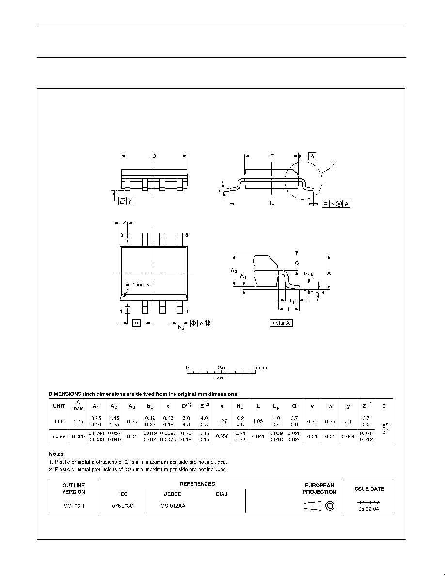
SO8:
plastic small outline package; 8 leads; body width 3.9mm
SOT96-1
Philips Semiconductors
Product specification
NE/SA5204A
Wide-band high-frequency amplifier
1992 Feb 25
13
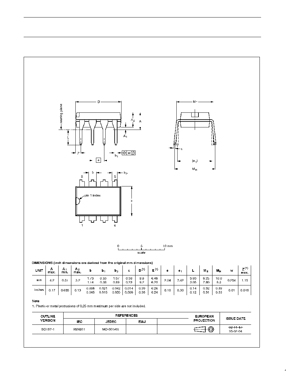
DIP8:
plastic dual in-line package; 8 leads (300 mil)
SOT97-1

Philips Semiconductors
Product specification
NE/SA5204A
Wide-band high-frequency amplifier
1992 Feb 25
14
Philips Semiconductors and Philips Electronics North America Corporation reserve the right to make changes, without notice, in the products,
including circuits, standard cells, and/or software, described or contained herein in order to improve design and/or performance. Philips
Semiconductors assumes no responsibility or liability for the use of any of these products, conveys no license or title under any patent, copyright,
or mask work right to these products, and makes no representations or warranties that these products are free from patent, copyright, or mask
work right infringement, unless otherwise specified. Applications that are described herein for any of these products are for illustrative purposes
only. Philips Semiconductors makes no representation or warranty that such applications will be suitable for the specified use without further testing
or modification.
LIFE SUPPORT APPLICATIONS
Philips Semiconductors and Philips Electronics North America Corporation Products are not designed for use in life support appliances, devices,
or systems where malfunction of a Philips Semiconductors and Philips Electronics North America Corporation Product can reasonably be expected
to result in a personal injury. Philips Semiconductors and Philips Electronics North America Corporation customers using or selling Philips
Semiconductors and Philips Electronics North America Corporation Products for use in such applications do so at their own risk and agree to fully
indemnify Philips Semiconductors and Philips Electronics North America Corporation for any damages resulting from such improper use or sale.
This data sheet contains preliminary data, and supplementary data will be published at a later date. Philips
Semiconductors reserves the right to make changes at any time without notice in order to improve design
and supply the best possible product.
Philips Semiconductors and Philips Electronics North America Corporation
register eligible circuits under the Semiconductor Chip Protection Act.
©
Copyright Philips Electronics North America Corporation 1993
All rights reserved. Printed in U.S.A.
Philips Semiconductors
811 East Arques Avenue
P.O. Box 3409
Sunnyvale, California 94088≠3409
Telephone 800-234-7381
DEFINITIONS
Data Sheet Identification
Product Status
Definition
Objective Specification
Preliminary Specification
Product Specification
Formative or in Design
Preproduction Product
Full Production
This data sheet contains the design target or goal specifications for product development. Specifications
may change in any manner without notice.
This data sheet contains Final Specifications. Philips Semiconductors reserves the right to make changes
at any time without notice, in order to improve design and supply the best possible product.