 | –≠–ª–µ–∫—Ç—Ä–æ–Ω–Ω—ã–π –∫–æ–º–ø–æ–Ω–µ–Ω—Ç: SA555 | –°–∫–∞—á–∞—Ç—å:  PDF PDF  ZIP ZIP |
Philips Semiconductors Linear Products
Product specification
NE/SA/SE555/SE555C
Timer
346
August 31, 1994
853-0036 13721
DESCRIPTION
The 555 monolithic timing circuit is a highly stable controller capable
of producing accurate time delays, or oscillation. In the time delay
mode of operation, the time is precisely controlled by one external
resistor and capacitor. For a stable operation as an oscillator, the
free running frequency and the duty cycle are both accurately
controlled with two external resistors and one capacitor. The circuit
may be triggered and reset on falling waveforms, and the output
structure can source or sink up to 200mA.
FEATURES
∑
Turn-off time less than 2
µ
s
∑
Max. operating frequency greater than 500kHz
∑
Timing from microseconds to hours
∑
Operates in both astable and monostable modes
∑
High output current
∑
Adjustable duty cycle
∑
TTL compatible
∑
Temperature stability of 0.005% per
∞
C
APPLICATIONS
∑
Precision timing
∑
Pulse generation
∑
Sequential timing
∑
Time delay generation
∑
Pulse width modulation
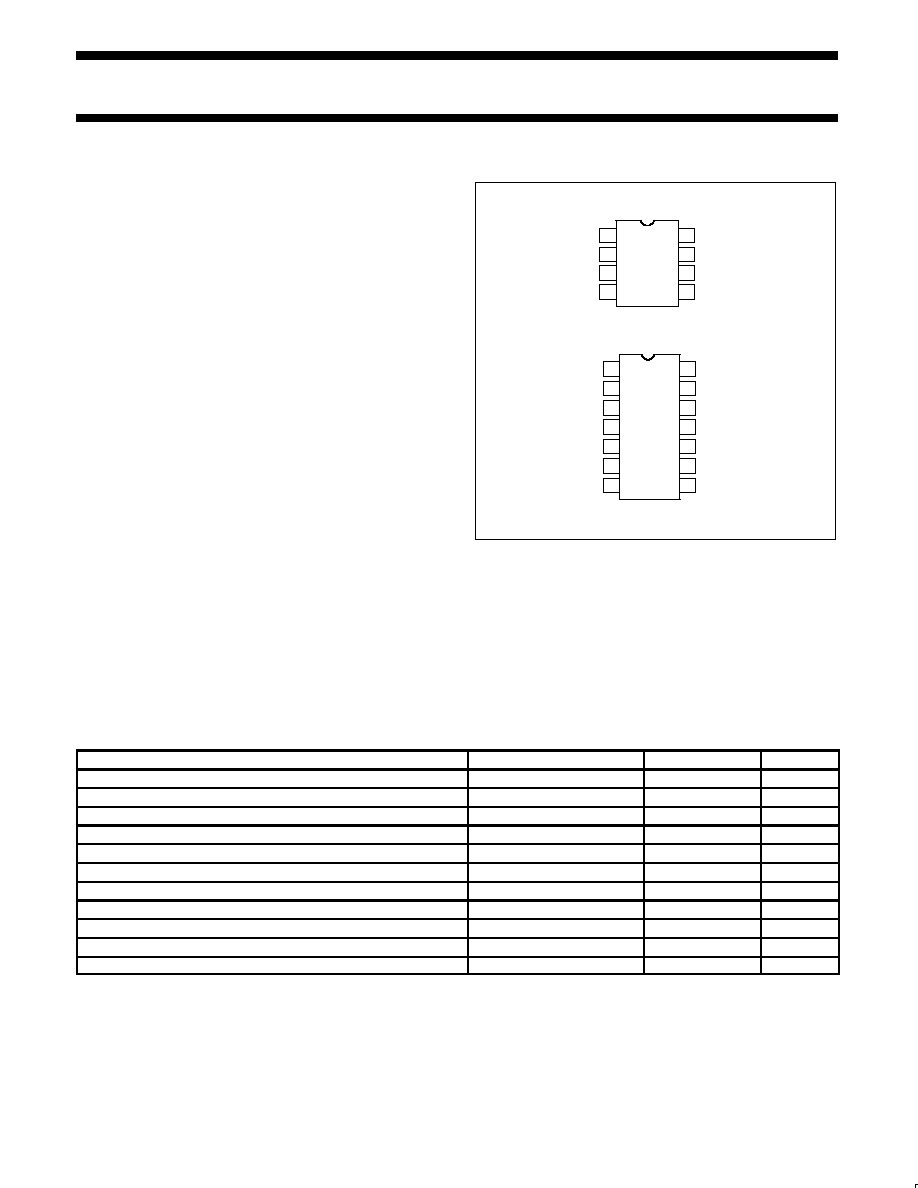
PIN CONFIGURATIONS
1
2
3
4
5
6
7
8
1
2
3
4
5
6
7
8
14
13
12
11
10
9
GND
TRIGGER
OUTPUT
RESET
GND
NC
TRIGGER
OUTPUT
NC
RESET
NC
DISCHARGE
THRESHOLD
CONTROL VOLTAGE
NC
DISCHARGE
NC
THRESHOLD
NC
CONTROL VOLTAGE
VCC
VCC
D, N, FE Packages
TOP VIEW
F Package
ORDERING INFORMATION
DESCRIPTION
TEMPERATURE RANGE
ORDER CODE
DWG #
8-Pin Plastic Small Outline (SO) Package
0 to +70
∞
C
NE555D
0174C
8-Pin Plastic Dual In-Line Package (DIP)
0 to +70
∞
C
NE555N
0404B
8-Pin Plastic Dual In-Line Package (DIP)
-40
∞
C to +85
∞
C
SA555N
0404B
8-Pin Plastic Small Outline (SO) Package
-40
∞
C to +85
∞
C
SA555D
0174C
8-Pin Hermetic Ceramic Dual In-Line Package (CERDIP)
-55
∞
C to +125
∞
C
SE555CFE
8-Pin Plastic Dual In-Line Package (DIP)
-55
∞
C to +125
∞
C
SE555CN
0404B
14-Pin Plastic Dual In-Line Package (DIP)
-55
∞
C to +125
∞
C
SE555N
0405B
8-Pin Hermetic Cerdip
-55
∞
C to +125
∞
C
SE555FE
14-Pin Ceramic Dual In-Line Package (CERDIP)
0 to +70
∞
C
NE555F
0581B
14-Pin Ceramic Dual In-Line Package (CERDIP)
-55
∞
C to +125
∞
C
SE555F
0581B
14-Pin Ceramic Dual In-Line Package (CERDIP)
-55
∞
C to +125
∞
C
SE555CF
0581B

Philips Semiconductors Linear Products
Product specification
NE/SA/SE555/SE555C
Timer
August 31, 1994
347
BLOCK DIAGRAM
COMPARATOR
COMPARATOR
FLIP FLOP
OUTPUT
STAGE
THRESH-
OLD
VCC
6
7
3
1
4
2
5
8
R
R
R
CONTROL
VOLTAGE
TRIGGER
RESET
DIS-
CHARGE
OUTPUT
GND
EQUIVALENT SCHEMATIC
NOTE:
Pin numbers are for 8-Pin package
CONTROL VOLTAGE
FM
VCC
R1
4.7K
R2
330
R3
4.7
K
R
4
1
K
R
7
5
K
R12
6.8K
Q21
Q9
Q8
Q7
Q6
Q5
Q1
Q2
Q3
Q4
Q19
Q22
R13
3.9K
OUTPUT
Q23
C
B
R1
0
82.
K
R5
10
K
Q10
Q11 Q12
Q13
Q20
R11
4.7K
CB
Q18
E
R8
5K
Q17
Q16
Q15
R6
100K
R16
100
Q14
Q25
R9
5K
R15
4.7K
Q24
R14
220
THRESHOLD
TRIGGER
RESET
DISCHARGE
GND
Philips Semiconductors Linear Products
Product specification
NE/SA/SE555/SE555C
Timer
August 31, 1994
348
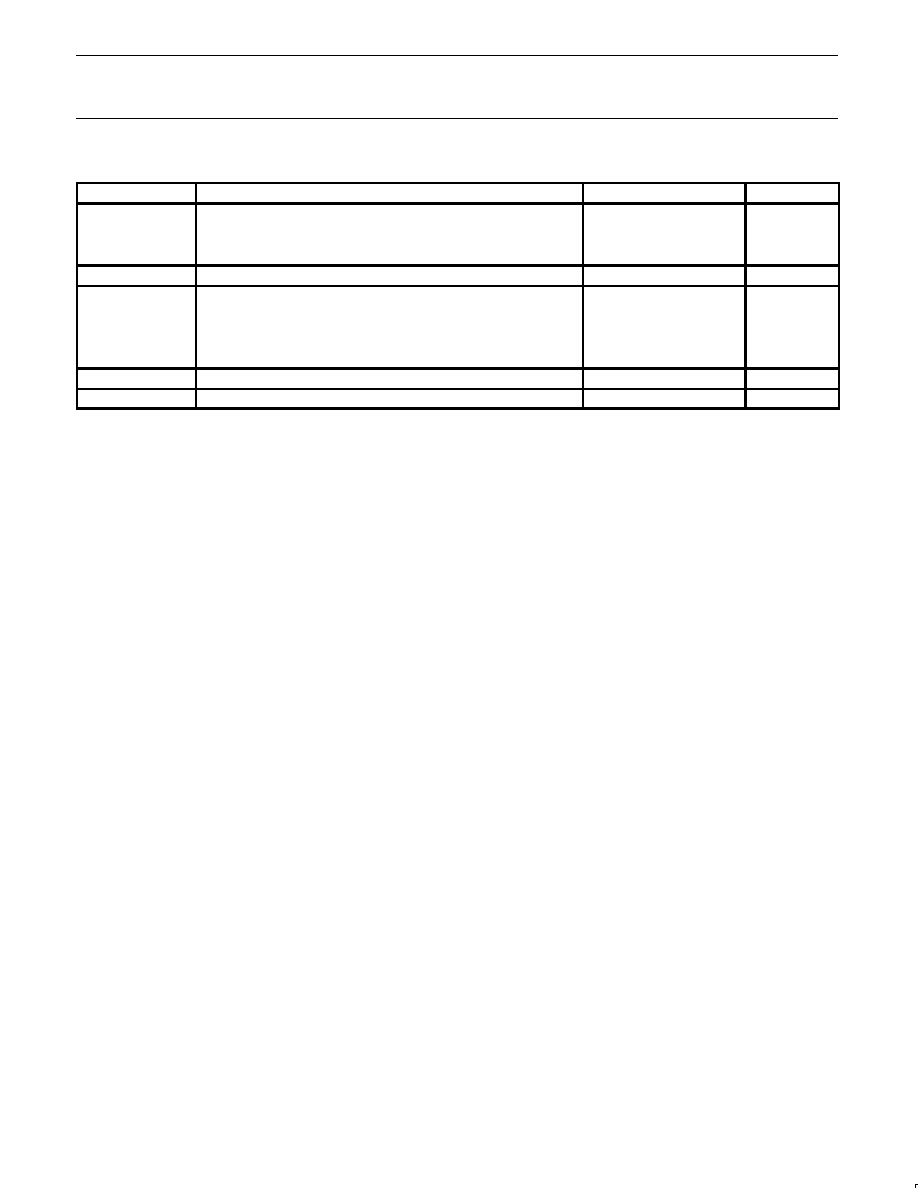
ABSOLUTE MAXIMUM RATINGS
SYMBOL
PARAMETER
RATING
UNIT
Supply voltage
V
CC
SE555
+18
V
NE555, SE555C, SA555
+16
V
P
D
Maximum allowable power dissipation
1
600
mW
T
A
Operating ambient temperature range
NE555
0 to +70
∞
C
SA555
-40 to +85
∞
C
SE555, SE555C
-55 to +125
∞
C
T
STG
Storage temperature range
-65 to +150
∞
C
T
SOLD
Lead soldering temperature (10sec max)
+300
∞
C
NOTES:
1. The junction temperature must be kept below 125
∞
C for the D package and below 150
∞
C for the FE, N and F packages. At ambient tempera-
tures above 25
∞
C, where this limit would be derated by the following factors:
D package 160
∞
C/W
FE package 150
∞
C/W
N package 100
∞
C/W
F package 105
∞
C/W
Philips Semiconductors Linear Products
Product specification
NE/SA/SE555/SE555C
Timer
August 31, 1994
349
DC AND AC ELECTRICAL CHARACTERISTICS
T
A
= 25
∞
C, V
CC
= +5V to +15 unless otherwise specified.
SYMBOL
PARAMETER
TEST CONDITIONS
SE555
NE555/SE555C
UNIT
SYMBOL
PARAMETER
TEST CONDITIONS
Min
Typ
Max
Min
Typ
Max
UNIT
V
CC
Supply voltage
4.5
18
4.5
16
V
I
CC
Supply current (low
V
CC
=5V, R
L
=
3
5
3
6
mA
state)
1
V
CC
=15V, R
L
=
10
12
10
15
mA
Timing error (monostable)
R
A
=2k
to 100k
t
M
Initial accuracy
2
C=0.1
µ
F
0.5
2.0
1.0
3.0
%
t
M
/
T
Drift with temperature
30
100
50
150
ppm/
∞
C
t
M
/
V
S
Drift with supply voltage
0.05
0.2
0.1
0.5
%/V
Timing error (astable)
R
A
, R
B
=1k
to 100k
t
A
Initial accuracy
2
C=0.1
µ
F
4
6
5
13
%
t
A
/
T
Drift with temperature
V
CC
=15V
500
500
ppm/
∞
C
t
A
/
V
S
Drift with supply voltage
0.15
0.6
0.3
1
%/V
V
C
Control voltage level
V
CC
=15V
9.6
10.0
10.4
9.0
10.0
11.0
V
V
CC
=5V
2.9
3.33
3.8
2.6
3.33
4.0
V
V
CC
=15V
9.4
10.0
10.6
8.8
10.0
11.2
V
V
TH
Threshold voltage
V
CC
=5V
2.7
3.33
4.0
2.4
3.33
4.2
V
I
TH
Threshold current
3
0.1
0.25
0.1
0.25
µ
A
V
TRIG
Trigger voltage
V
CC
=15V
4.8
5.0
5.2
4.5
5.0
5.6
V
V
CC
=5V
1.45
1.67
1.9
1.1
1.67
2.2
V
I
TRIG
Trigger current
V
TRIG
=0V
0.5
0.9
0.5
2.0
µ
A
V
RESET
Reset voltage
4
V
CC
=15V, V
TH
=10.5V
0.3
1.0
0.3
1.0
V
I
RESET
Reset current
V
RESET
=0.4V
0.1
0.4
0.1
0.4
mA
Reset current
V
RESET
=0V
0.4
1.0
0.4
1.5
mA
V
CC
=15V
I
SINK
=10mA
0.1
0.15
0.1
0.25
V
I
SINK
=50mA
0.4
0.5
0.4
0.75
V
V
OL
Output voltage (low)
I
SINK
=100mA
2.0
2.2
2.0
2.5
V
I
SINK
=200mA
2.5
2.5
V
V
CC
=5V
I
SINK
=8mA
0.1
0.25
0.3
0.4
V
I
SINK
=5mA
0.05
0.2
0.25
0.35
V
V
CC
=15V
I
SOURCE
=200mA
12.5
12.5
V
V
OH
Output voltage (high)
I
SOURCE
=100mA
13.0
13.3
12.75
13.3
V
V
CC
=5V
I
SOURCE
=100mA
3.0
3.3
2.75
3.3
V
t
OFF
Turn-off time
5
V
RESET
=V
CC
0.5
2.0
0.5
2.0
µ
s
t
R
Rise time of output
100
200
100
300
ns
t
F
Fall time of output
100
200
100
300
ns
Discharge leakage current
20
100
20
100
nA
NOTES:
1. Supply current when output high typically 1mA less.
2. Tested at V
CC
=5V and V
CC
=15V.
3. This will determine the max value of R
A
+R
B
, for 15V operation, the max total R=10M
, and for 5V operation, the max. total R=3.4M
.
4. Specified with trigger input high.
5. Time measured from a positive going input pulse from 0 to 0.8
◊
V
CC
into the threshold to the drop from high to low of the output. Trigger is
tied to threshold.
Philips Semiconductors Linear Products
Product specification
NE/SA/SE555/SE555C
Timer
August 31, 1994
350
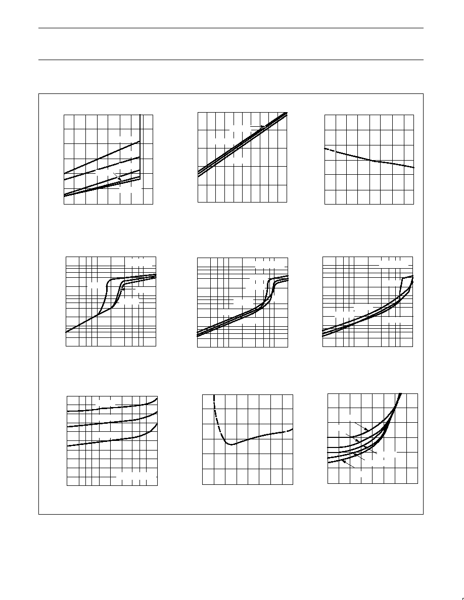
TYPICAL PERFORMANCE CHARACTERISTICS
Minimum Pulse Width
Required for Triggering
Supply Current
vs Supply Voltage
Low Output Voltage
vs Output Sink Current
Low Output Voltage
vs Output Sink Current
Low Output Voltage
vs Output Sink Current
Delay Time
vs Temperature
Delay Time
vs Supply Voltage
Propagation Delay vs Voltage
Level of Trigger Pulse
High Output Voltage Drop
vs Output Source Current
MINIMUM PULSE WIDTH (ns)
LOWEST VOLTAGE LEVEL OF TRIGGER PULSE
150
125
100
75
50
25
0
0
0.1
0.2
0.3
0.4 (XVCC)
-55
o
C
0
o
C
+25
o
C
+70
o
C
+125
o
C
10.0
8.0
6.0
4.0
2.0
0
5.0
10.0
15.0
SUPPLY VOLTAGE ≠ VOLTS
SUPPL
Y
CURRENT ≠ mA
1.015
1.010
1.005
1.000
0.995
0.990
0.985
-50
-25
0
+25 +50
+75 +100 +125
NORMALIZED DELA
Y
TIME
TEMPERATURE ≠
o
C
10
1.0
0.1
0.001
1.0
2.0
5.0
10
20
50
100
10
1.0
0.1
0.01
1.0
2.0
5.0
10
20
50
100
10
1.0
0.1
0.01
1.0
2.0
5.0
10
20
50
100
1.0
2.0
5.0
10
20
50
100
2.0
1.8
1.6
1.4
1.2
1.0
0.8
0.6
0.4
0.2
0
1.015
1.010
1.005
1.000
0.995
0.990
0.985
0
5
10
15
20
0
0.1
0.2
0.3
0.4
300
250
200
150
100
50
0
V ≠ VOL
TS
OUT
V ≠ VOL
TS
OUT
V ≠ VOL
TS
OUT
V ≠ VOL
TS
OUT
V
CC
NORMALIZED DELA
Y
TIME
PROP
AGA
TION DELA
Y
≠ ns
ISINK ≠ mA
ISINK ≠ mA
ISINK ≠ mA
ISOURCE ≠ mA
SUPPLY VOLTAGE ≠ V
LOWEST VOLTAGE LEVEL
OF TRIGGER PULSE ≠ XVCC
+125
o
C
+25
o
C
-55
o
C
VCC = 5V
VCC = 10V
VCC = 15V
-55
o
C
+25
o
C
+25
o
C
-55
o
C
+25
o
C
+25
o
C
+25
o
C
+25
o
C
-55
o
C
-55
o
C
55
o
C
+25
o
C
+25
o
C
≠55
o
C
+25
o
C
+125
o
C
5V
VCC
15V
-55
o
C
0
o
C
+25
o
C
+70
o
C
+25
o
C
Philips Semiconductors Linear Products
Product specification
NE/SA/SE555/SE555C
Timer
August 31, 1994
351
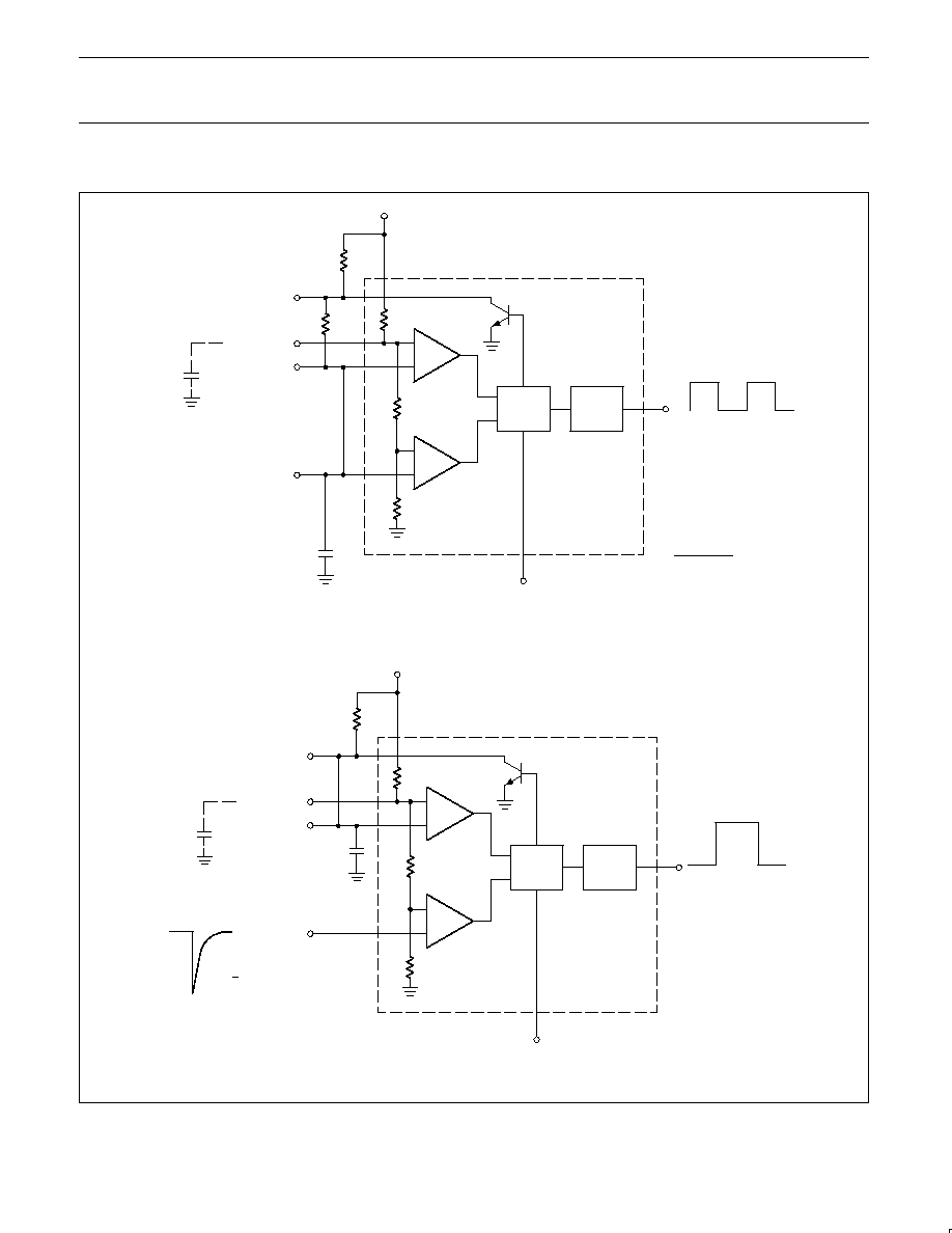
TYPICAL APPLICATIONS
OUTPUT
FLIP
FLOP
COMP
COMP
f
+
1.49
(R
A
)
2R
B
)C
555 OR 1/2 556
DISCHARGE
CONTROL
VOLTAGE
THRESHOLD
TRIGGER
RESET
OUTPUT
R
R
C
RB
RA
R
5
6
2
4
3
8
7
.01
µ
F
VCC
OUTPUT
FLIP
FLOP
COMP
COMP
555 OR 1/2 556
DISCHARGE
CONTROL
VOLTAGE
THRESHOLD
TRIGGER
RESET
OUTPUT
R
R
RA
R
5
6
2
4
3
8
7
.01
µ
F
VCC
T = 1.1RC
C
*
1
3
V
CC
|
t |
Astable Operation
Monostable Operation
Philips Semiconductors Linear Products
Product specification
NE/SA/SE555/SE555C
Timer
August 31, 1994
352
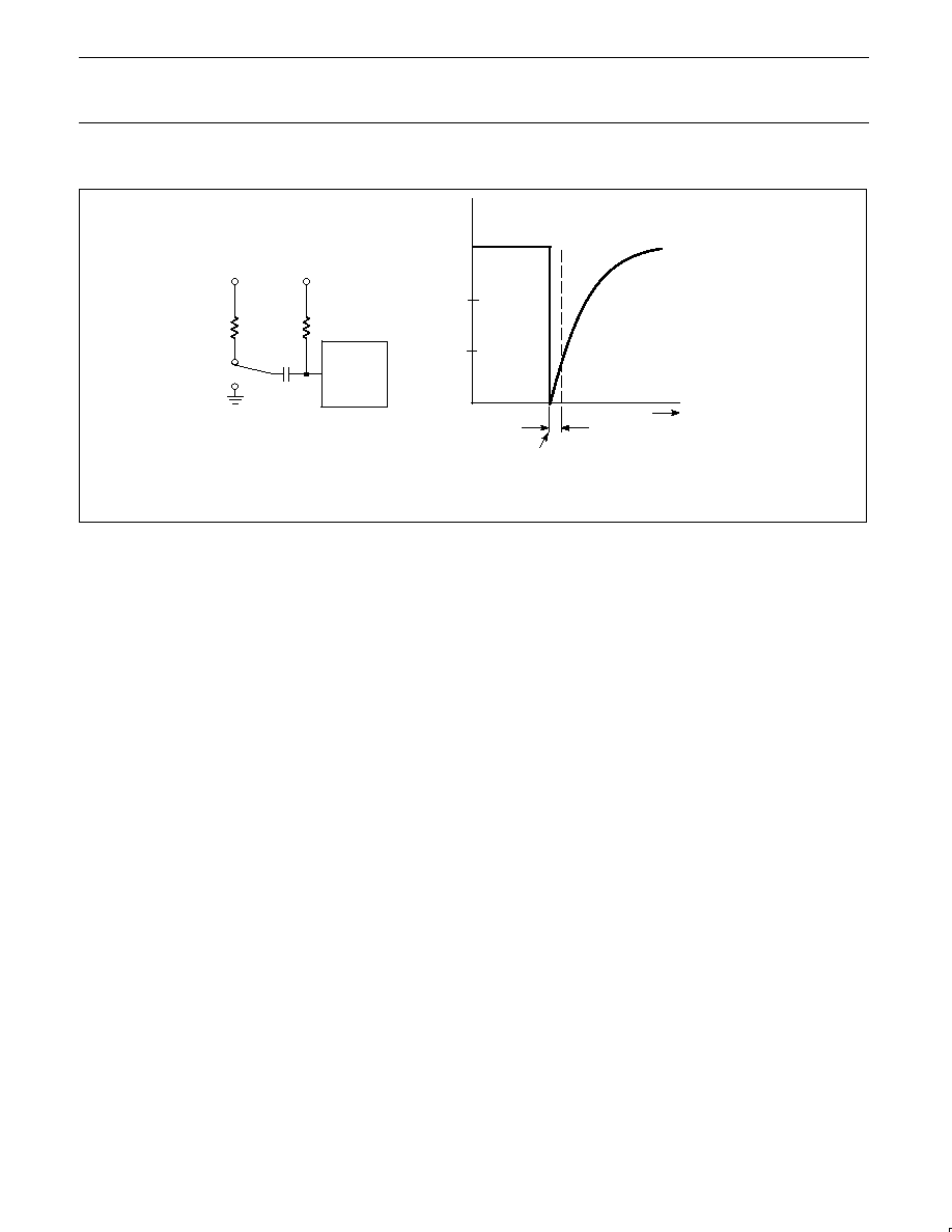
TYPICAL APPLICATIONS
DURATION OF
TRIGGER PULSE AS
SEEN BY THE TIMER
VCC
VCC
10k
2
555
.001
µ
F
NOTE: All resistor values are in
Figure 1. AC Coupling of the Trigger Pulse
1
SWITCH GROUNDED
AT THIS POINT
OVOLTS
1/3 VCC
VCC
Trigger Pulse Width Requirements and Time
Delays
Due to the nature of the trigger circuitry, the timer will trigger on the
negative going edge of the input pulse. For the device to time out
properly, it is necessary that the trigger voltage level be returned to
some voltage greater than one third of the supply before the time out
period. This can be achieved by making either the trigger pulse
sufficiently short or by AC coupling into the trigger. By AC coupling
the trigger, see Figure 1, a short negative going pulse is achieved
when the trigger signal goes to ground. AC coupling is most
frequently used in conjunction with a switch or a signal that goes to
ground which initiates the timing cycle. Should the trigger be held
low, without AC coupling, for a longer duration than the timing cycle
the output will remain in a high state for the duration of the low
trigger signal, without regard to the threshold comparator state. This
is due to the predominance of Q
15
on the base of Q
16
, controlling
the state of the bi-stable flip-flop. When the trigger signal then
returns to a high level, the output will fall immediately. Thus, the
output signal will follow the trigger signal in this case.
Another consideration is the "turn-off time". This is the measurement
of the amount of time required after the threshold reaches 2/3 V
CC
to turn the output low. To explain further, Q
1
at the threshold input
turns on after reaching 2/3 V
CC
, which then turns on Q
5
, which turns
on Q
6
. Current from Q
6
turns on Q
16
which turns Q
17
off. This
allows current from Q
19
to turn on Q
20
and Q
24
to given an output
low. These steps cause the 2
µ
s max. delay as stated in the data
sheet.
Also, a delay comparable to the turn-off time is the trigger release
time. When the trigger is low, Q
10
is on and turns on Q
11
which turns
on Q
15
. Q
15
turns off Q
16
and allows Q
17
to turn on. This turns off
current to Q
20
and Q
24
, which results in output high. When the
trigger is released, Q
10
and Q
11
shut off, Q
15
turns off, Q
16
turns on
and the circuit then follows the same path and time delay explained
as "turn off time". This trigger release time is very important in
designing the trigger pulse width so as not to interfere with the
output signal as explained previously.