
1.
General description
The SA56202 is a one-chip motor driver IC that is capable to drive all motors of CD or
DVD systems: spindle, sled and loading motors and actuators on the optical pick-up unit.
The driver intended for the 3-phase, brushless, Hall-commutated spindle motor uses
True-Silent PWM. This proprietary technology ensures that all 3-phase motor currents are
sinusoidal resulting in an optimally silent driver. Internal regeneration of the back-EMF of
the spindle motor enables the driver to operate in current-steering mode without using
external power-dissipating sense resistors. The driver intended for the 2-phase sled
stepper motor operates in current-steering PWM mode. In addition the IC contains four
full-bridge linear channels that can be used to drive a loading motor and 3D actuators
(focus, tracking and tilt).
The SA56202 is available in an exposed die pad HTSSOP56 package.
2.
Features
s
True-Silent PWM spindle motor driver
s
Low heat generation due to power-efficient direct full-bridge switching of spindle motor
driver
s
Controlled spindle motor current during acceleration and brake
s
Reverse torque brake function (full bridge)
s
Adjustable spindle motor current limiter
s
Internal regeneration for EMF of spindle motor
s
Current-steering PWM controlled stepper motor driver for sled
s
Four class-AB linear channels for loading motor and 3D actuators (focus, tracking and
tilt)
s
Low on-resistance D-MOSFET output power stages
s
Built-in thermal shutdown, thermal warning and temperature diode
s
Interfaces to 3 V and 5 V logic
s
Package with low thermal resistance to heatsink (reflowable die pad).
3.
Applications
s
DVD+RW, DVD-RW, DVD-ROM and DVD-RAM
s
Combi
s
CD-ROM and CD-RW
s
Other compact disk media.
SA56202
One-chip motor driver
Rev. 01 -- 19 July 2004
Preliminary data sheet

9397 750 12772
� Koninklijke Philips Electronics N.V. 2004. All rights reserved.
Preliminary data sheet
Rev. 01 -- 19 July 2004
2 of 24
Philips Semiconductors
SA56202
One-chip motor driver
4.
Ordering information
Table 1:
Ordering information
Type number
Package
Name
Description
Version
SA56202TW
HTSSOP56 plastic thermal enhanced thin shrink small outline package; 56 leads;
body width 6.1 mm; exposed die pad
SOT793-1

9397 750 12772
� Koninklijke Philips Electronics N.V. 2004. All rights reserved.
Preliminary data sheet
Rev. 01 -- 19 July 2004
3 of 24
Philips Semiconductors
SA56202
One-chip motor driver
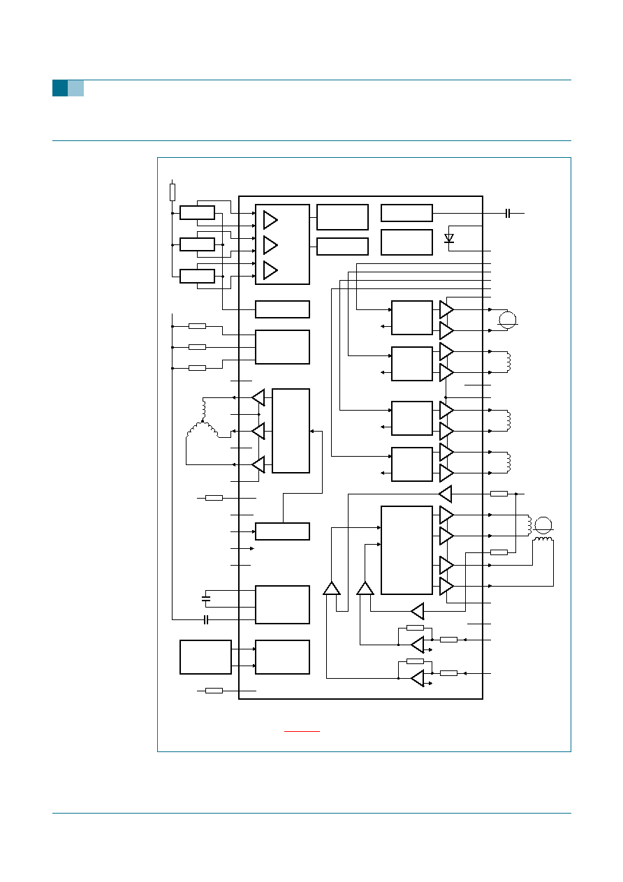
5.
Block diagram
Fig 1.
Block diagram.
001aaa429
REVERSE
DETECTION
LEVEL
SHIFT
LEVEL
SHIFT
LEVEL
SHIFT
LEVEL
SHIFT
SLED
LOGIC
CURRENT
REFERENCE
FG
OSCILLATOR
THERMAL
SHUTDOWN
FG
HALL BIAS
ADC
CHARGE
PUMP
MUTE/
STANDBY
FUNCTIONS
SPINDLE
LOGIC
HALL
AMP
1
2
3
4
5
6
7
8
9
10
11
12
13
15
14
16
17
18
28
19
20
21
22
23
24
25
26
27
DIODE
47 k
VINREF
VINREF
VINREF
VINREF
VINREF
VINREF
VINREF
SA56202
V
SS(DIO)
VINLD
COSC
HU
+
HU
-
HV
+
HV
-
HW
+
HW
-
HBIAS
RREF
REMF
RLIM
V
SS1(SPN)
U
V
DD1(SPN)
V
V
SS2(SPN)
W
V
DD2(SPN)
FG
V
SSD
VINSPN
VINREF
V
DDA
CP1
CP2
CP3
CTL1
CTL2
TEMP
VINFCS
VINTRK
VINTLT
V
DD(LD)
LDO
+
LDO
-
V
SS(LIN)
V
DD(ACT)
TLTO
-
TRKO
-
TRKO
+
FCSO
-
FCSO
+
TLTO
+
RSLD1
RSLD2
SLDO2
-
SLDO2
+
SLDO1
-
SLDO1
+
V
DD(SLD)
V
SSA
VINSLD1
VINSLD2
31
30
29
33
32
34
35
36
37
38
39
40
41
42
43
44
45
46
47
48
49
50
51
52
53
54
55
56
47 k
9397 750 12772
� Koninklijke Philips Electronics N.V. 2004. All rights reserved.
Preliminary data sheet
Rev. 01 -- 19 July 2004
4 of 24
Philips Semiconductors
SA56202
One-chip motor driver
6.
Pinning information
6.1 Pinning
6.2 Pin description
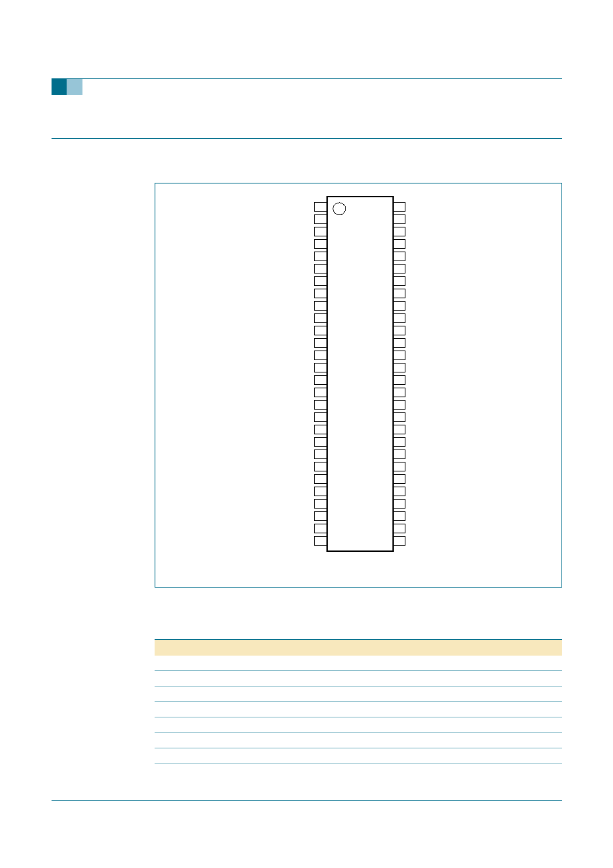
Fig 2.
Pin configuration.
SA56202TW
001aaa458
1
2
3
4
5
6
7
8
9
10
11
12
13
14
15
16
17
18
19
20
21
22
23
24
25
26
27
28
56
55
54
53
52
51
50
49
48
47
46
45
44
43
42
41
40
39
38
37
36
35
34
33
32
31
30
29
DIODE
V
SS(DIO)
VINLD
COSC
HU
+
HU
-
HV
+
HV
-
HW
+
HW
-
HBIAS
RREF
REMF
RLIM
V
SS1(SPN)
U
V
DD1(SPN)
V
V
SS2(SPN)
W
V
DD2(SPN)
FG
V
SSD
VINSPN
VINREF
V
DDA
CP1
CP2
CP3
CTL1
CTL2
TEMP
VINFCS
VINTRK
VINTLT
V
DD(LD)
LDO
+
LDO
-
V
SS(LIN)
V
DD(ACT)
TLTO
-
TRKO
-
TRKO
+
FCSO
-
FCSO
+
TLTO
+
RSLD1
RSLD2
SLDO2
-
SLDO2
+
SLDO1
-
SLDO1
+
V
DD(SLD)
V
SSA
VINSLD1
VINSLD2
Table 2:
Pin description
Symbol
Pin
Description
HU+
1
Hall input U positive
HU
-
2
Hall input U negative
HV+
3
Hall input V positive
HV
-
4
Hall input V negative
HW+
5
Hall input W positive
HW
-
6
Hall input W negative
HBIAS
7
Hall element bias
RREF
8
external resistor for current reference

9397 750 12772
� Koninklijke Philips Electronics N.V. 2004. All rights reserved.
Preliminary data sheet
Rev. 01 -- 19 July 2004
5 of 24
Philips Semiconductors
SA56202
One-chip motor driver
REMF
9
external resistor for EMF regeneration
RLIM
10
external resistor for current limit
V
SS1(SPN)
11
spindle driver ground 1
U
12
spindle driver output U
V
DD1(SPN)
13
spindle driver supply voltage 1
V
14
spindle driver output V
V
SS2(SPN)
15
spindle driver ground 2
W
16
spindle driver output W
V
DD2(SPN)
17
spindle driver supply voltage 2
FG
18
frequency generator output
V
SSD
19
digital ground
VINSPN
20
spindle driver input voltage for spindle motor current
VINREF
21
reference input voltage for all motor drivers
V
DDA
22
analog supply voltage
CP1
23
charge pump capacitor connection 1
CP2
24
charge pump capacitor connection 2
CP3
25
charge pump capacitor connection 3
CTL1
26
driver logic control input 1
CTL2
27
driver logic control input 2
TEMP
28
thermal warning
VINSLD1
29
sled driver 1 input voltage for sled motor current
VINSLD2
30
sled driver 2 input voltage for sled motor current
V
SSA
31
analog ground
V
DD(SLD)
32
sled driver supply voltage
SLD2O
-
33
sled driver output 2 negative
SLDO2+
34
sled driver output 2 positive
RSLD2
35
external sense resistor for sled driver 2 current sense
SLDO1
-
36
sled driver output 1 negative
SLDO1+
37
sled driver output 1 positive
RSLD1
38
external sense resistor for sled driver 1 current sense
TLTO
-
39
tilting driver output negative
TLTO+
40
tilting driver output positive
TRKO
-
41
tracking driver output negative
TRKO+
42
tracking driver output positive
V
DD(ACT)
43
actuator drivers supply voltage
V
SS(LIN)
44
linear drivers ground
FCSO
-
45
focus driver output negative
FCSO+
46
focus driver output positive
LDO
-
47
loading driver output negative
LDO+
48
loading driver output positive
V
DD(LD)
49
loading driver supply voltage
Table 2:
Pin description
...continued
Symbol
Pin
Description
9397 750 12772
� Koninklijke Philips Electronics N.V. 2004. All rights reserved.
Preliminary data sheet
Rev. 01 -- 19 July 2004
6 of 24
Philips Semiconductors
SA56202
One-chip motor driver
7.
Functional description
7.1 Spindle motor control
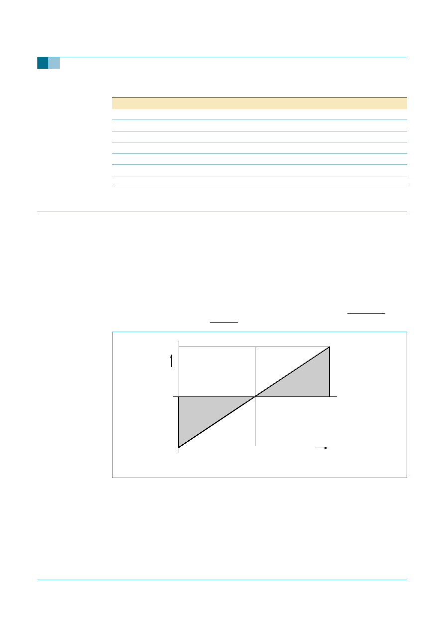
The control input voltage on pin VINSPN is converted into a digital value by the ADC
where the voltage on pin VINREF is the midpoint reference. The transconductance gain
from input voltage V
VINSPN
to output motor current I
MOT
is:
where I
LIM
can be programmed by means of external resistor R
LIM
; see
Section 7.4
. The
motor current is described by
Figure 3
.
For VINSPN voltages larger than V
VINREF
the motor will accelerate with forward torque
control. For VINSPN voltages smaller than V
VINREF
the motor will brake with reverse
torque control. Because the U, V and W half-bridges of the spindle motor driver use a
direct PWM full-bridge switching scheme, the motor current can also be controlled and
limited during brake. Note that because of this active brake mechanism energy of the
motor can be recuperated back to the supply. Especially at large speeds, this can result in
currents delivered back to the supply. If the supply and/or other circuits than the motor
VINTLT
50
tilting driver input for tilt actuator voltage
VINTRK
51
tracking driver input for tracking actuator voltage
VINFCS
52
focus driver input for focus actuator voltage
VINLD
53
loading driver input for loading motor voltage
V
SS(DIO)
54
temperature diode ground
DIODE
55
diode for temperature readout
COSC
56
external capacitor for internal oscillator
Table 2:
Pin description
...continued
Symbol
Pin
Description
Fig 3.
Spindle motor current as a function of control input voltage on pin VINSPN.
g
m(SP N
)
I
MOT
V
VINSPN
V
VINREF
�
-------------------------------------------------
I
LIM
V
VINREF
---------------------
=
=
001aaa431
I
LIM
I
MOT
V
VINSPN
-
I
LIM
reverse
torque
brake
0
V
VINREF
2V
VINREF
forward
torque
9397 750 12772
� Koninklijke Philips Electronics N.V. 2004. All rights reserved.
Preliminary data sheet
Rev. 01 -- 19 July 2004
7 of 24
Philips Semiconductors
SA56202
One-chip motor driver
driver do not use this recuperated current, than the supply voltage can possibly rise to
unacceptable values. In that case it is recommended to lower the spindle current during
brake by means of the VINSPN setting.
Upon detection of reverse detection all U, V and W driver outputs are connected to
V
DD(SPN)
. This short brake prevents the motor of spinning backwards.
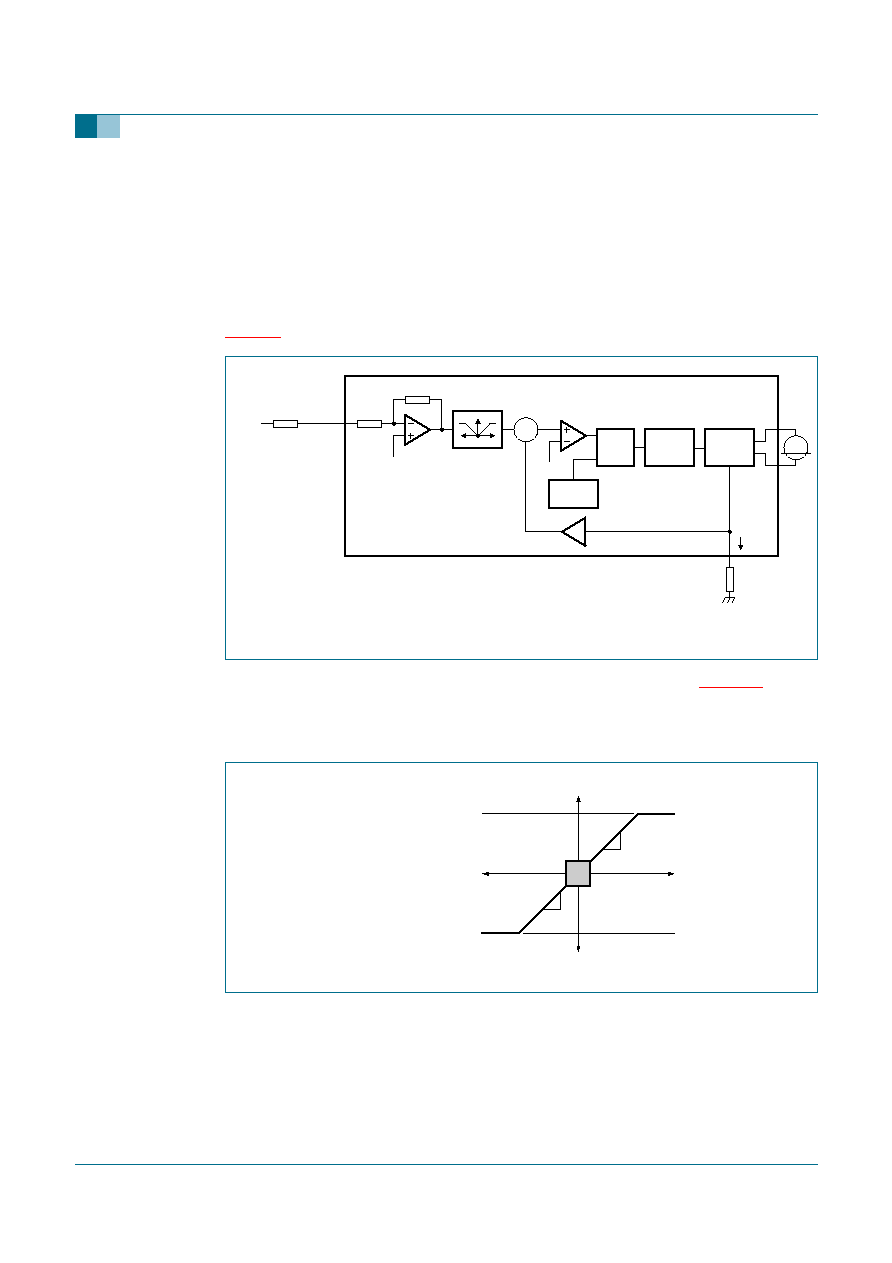
7.2 Internal regeneration of back-EMF spindle motor
The spindle motor driver uses the information from the Hall sensors to internally
regenerate the back-EMF of the motor. See
Figure 4
.
Rotational speed
is derived from the Hall event frequency. Multiplying
with the k-factor
of the motor gives the back-EMF voltage V
EMF
. This V
EMF
is added to the current-limit
scaled spindle input voltage V
VINSPN
. This sum V
MOT
steers the PWM outputs U, V and W.
The result is that the input voltage V
VINSPN
sets the current through the motor. This
explains how the SA56202 spindle motor driver exhibits a current control transfer function
without using external sense resistors.
The simplified motor schematic in
Figure 5
shows the series resistance and back-EMF
voltage of the motor.
Fig 4.
Regeneration of back-EMF voltage spindle motor.
Fig 5.
Simplified spindle motor schematic.
001aaa438
PWM
SPEED
U
V
W
Hall U
spindle
motor
V
MOT
= V
RI
+ V
EMF
V
RI
= R
m
�
I
m
V
EMF
=
�
k
Hall V
Hall W
DIGITAL DOMAIN
VINSPN
torque
control
signal
R
LIM
maximum
motor
current
R
EMF
motor
k-factor
ANALOG DOMAIN
A
D
A
D
A
D
001aaa450
V
M1
V
M2
V
RM
V
RM
V
EMF
2
V
EMF
2

9397 750 12772
� Koninklijke Philips Electronics N.V. 2004. All rights reserved.
Preliminary data sheet
Rev. 01 -- 19 July 2004
8 of 24
Philips Semiconductors
SA56202
One-chip motor driver
Figure 6
depicts the motor voltages V
M1
and V
M2
during accelerating and braking. The
back-EMF voltage is part of these motor voltages.
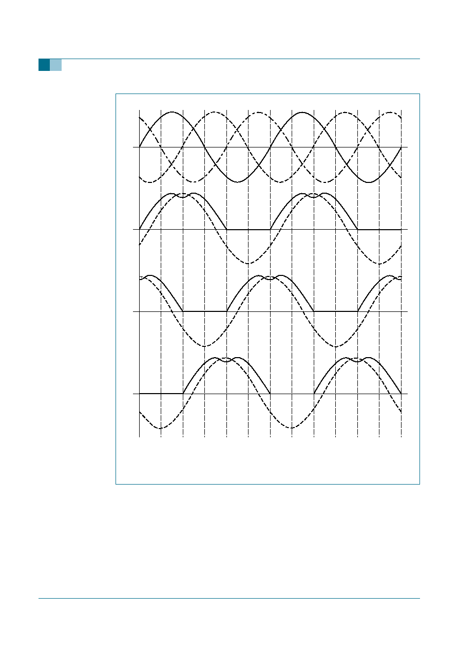
7.3 Sine generation using True-Silent signals
For the phase relation between the Hall inputs and the spindle outputs in forward rotation,
see
Figure 7
. These are the signal shapes in sine mode using our True-Silent PWM
technology. The particular shape of the 120
�
symmetrical U, V and W steering voltages
are because of improved drive strength and improved power efficiency. The drive strength
is improved because with this signal shape a 15 % larger sine can be fit within the supply
rails compared to direct-written sine signals. Also the power efficiency is improved
because this signal shape has 33 % less switching losses compared to a direct-written
sine.
The result is that the motor currents (and motor torques) are pure sine waves generated in
such a way that the motor is driven optimally silent, optimally power efficient and with
maximum driving strength.
Fig 6.
Motor voltages when accelerating and braking with constant motor current.
001aaa432
V
M2
accelerating
braking
V
RM
V
RM
V
M1
V
M1
V
M2
V
EMF
2
V
EMF
2
V
DD(SPN)
2
V
DD(SPN)
0
0
max
0
k
9397 750 12772
� Koninklijke Philips Electronics N.V. 2004. All rights reserved.
Preliminary data sheet
Rev. 01 -- 19 July 2004
9 of 24
Philips Semiconductors
SA56202
One-chip motor driver
7.4 Programming R
LIM
If the supply is connected between the terminals of a non-running spindle motor, then
usually a current will flow that is too large. The motor current can be limited to a value I
LIM
.
This I
LIM
can be programmed by means of R
LIM
. In order to calculate the required R
LIM
first a typical maximum motor current I
MAX
needs to be determined:
Fig 7.
Phase relation between Hall input signals and spindle motor driver output
voltages U(V), V(V), W(V) and motor currents U(I), V(I), W(I) in forward rotation
mode.
001aaa433
W
V
HALL U
U(V)
U(I)
V(V)
V(I)
W(V)
W(I)
HALL W
HALL V
U
I
MAX
V
DD SPN
(
)
R
motor
R
switches
+
--------------------------------------------
=
9397 750 12772
� Koninklijke Philips Electronics N.V. 2004. All rights reserved.
Preliminary data sheet
Rev. 01 -- 19 July 2004
10 of 24
Philips Semiconductors
SA56202
One-chip motor driver
I
LIM
can be chosen to be a fraction of this maximum current I
MAX
. By making the ratio
between R
LIM
(connected to pin 10) and R
REF
(connected to pin 8) this same fraction, I
LIM
is programmed as expressed in the following formula:
So by choosing I
LIM
, R
LIM
needs to be:
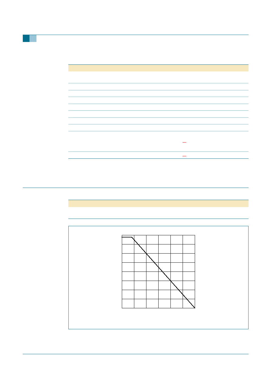
Figure 8
shows the limit current as a function of R
LIM
with R
REF
= 47 k
.
During accelerating and braking the motor current will not exceed I
LIM
. I
LIM
also sets the
transconductance gain I
LIM
/V
VINREF
of the spindle driver.
7.5 Programming R
EMF
The back-EMF voltage is internally regenerated. The ratio between R
EMF
and R
REF
is
used to scale the internal EMF regeneration. The value of external resistor R
EMF
depends
on the type of motor (k-factor and number of pole pairs N
PP
) and the motor supply voltage
V
DD(SPN)
. The following formula should be used to determine the R
EMF
resistor:
with k in units Nm/A.
7.6 FG generator
The raw zero-crossings of the Hall sensors are first filtered and debounced before being
passed to the FG generator. The FG generator toggles its output at every filtered Hall
zero-crossing. For three Hall sensors this means that the motor frequency is linked to the
FG frequency by:
Fig 8.
Limit current I
LIM
as a function of external resistor R
LIM
.
I
LIM
R
LIM
R
REF
-------------
I
MAX
�
=
R
LIM
I
LIM
I
MAX
------------
R
REF
�
=
R
LIM
(k
)
0
50
40
20
30
10
001aaa434
40
60
20
80
100
0
I
LIM
(% of I
MAX
)
R
EMF
k
2.6
�
10
3
�
R
REF
�
N
PP
V
DD SPN
(
)
�
--------------------------------------------------
=
f
motor
FG
3
N
PP
�
-------------------
=
9397 750 12772
� Koninklijke Philips Electronics N.V. 2004. All rights reserved.
Preliminary data sheet
Rev. 01 -- 19 July 2004
11 of 24
Philips Semiconductors
SA56202
One-chip motor driver
where N
PP
indicates the number of pole pairs of the motor. FG has an open-drain output
for easy interfacing to 3 V and 5 V logic.
7.7 Sled motor driver
Two current-steering PWM channels are available to drive a stepper motor. Per channel
an external sense resistor R
sense
is used that is connected to ground. A peak-current
control loop is implemented that modulates the duty cycle of the PWM signal. See
Figure 9
.
The clock generator has a nominal frequency of f
osc
/256 = 70 kHz. See
Figure 10
for the
transfer function from input voltage V
VINSLD
to output current at a typical R
sense
of 0.5
.
Input-to-output transconductance gain can be scaled down by connecting an external
resistor R
ext
in series with the input VINSLD.
Both limit current and transconductance gain are related to R
sense
in the following way:
Transconductance gain,
Limit current,
Fig 9.
Peak-current control architecture of stepper motor driver.
Fig 10. Transfer function of stepper motor driver.
001aaa435
M
R
S
Q
CLOCK
70 kHz
LOGIC
DRIVE
DRIVER
A
VINSLD
Rsense
IO
Rext
47 k
+
-
47 k
V
VINREF
input amplifier
V
VINREF
001aaa436
V
VINSLD
-
V
VINREF
(V)
-
1 A
+
1 A/V
+
1 A/V
1 A
I
OUT
(A)
dead zone
30 mV
-
30 mV
I
o
V
in
--------
1
2
R
sense
�
------------------------
=
I
LIM
1V
2
R
sense
�
------------------------
=
9397 750 12772
� Koninklijke Philips Electronics N.V. 2004. All rights reserved.
Preliminary data sheet
Rev. 01 -- 19 July 2004
12 of 24
Philips Semiconductors
SA56202
One-chip motor driver
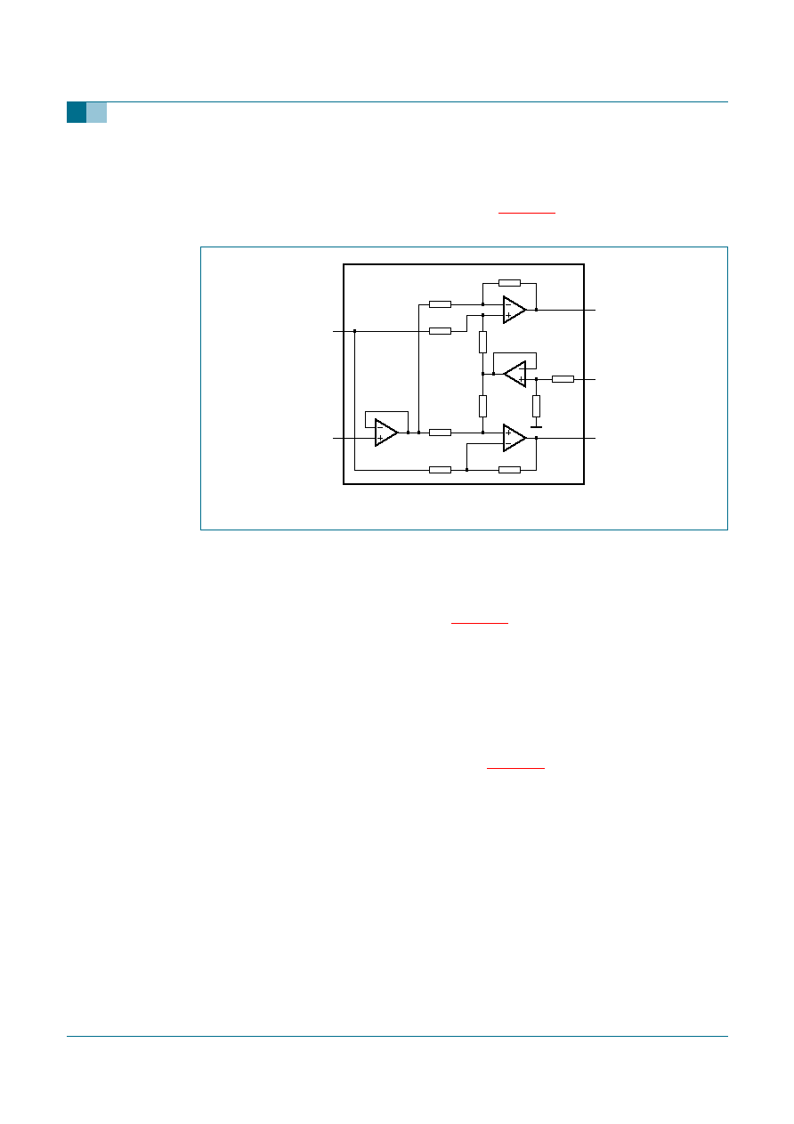
7.8 Loading motor driver
One of the linear channels is available to drive a DC loading motor. Pin V
DD(LD)
is used to
set the supply voltage for the loading motor driver.
Figure 11
depicts the voltage-steering
bridge topology of the SA56202.
7.9 Actuator motor drivers
Three linear channels are available to drive 3D actuators: focus, tracking and tilt. A pin
V
DD(ACT)
is used to set the supply voltage for these actuator drivers. The voltage-steering
bridge topology is the same as depicted in
Figure 11
. The mismatch of the voltage gain of
these 3 linear channels is guaranteed to be less than 5 %.
7.10 Charge pump
The on-board charge pump generates a regulated voltage of typically 18.2 V by using the
V
DD(SPN)
supply voltage. This boosted voltage is used to turn on the upper n-type DMOS
transistors of the output stages of the spindle driver, sled driver, loading driver and
actuator drivers. Recommended values for the pump-and-hold capacitor are 10 nF and
22 nF respectively (see also application diagram
Figure 13
). The charge pump should not
be loaded with other components or circuitry than these capacitors.
7.11 Thermal protection
If the junction temperature of the SA56202 exceeds 150
�
C, then a thermal warning signal
is given at pin TEMP. TEMP has an active-LOW open-drain output for easy interfacing to
3 V and 5 V logic. The temperature hysteresis for the thermal warning is 10
�
C. If the
junction temperature of the IC rises to 160
�
C, then a thermal shutdown is activated that
sets all power outputs in 3-state. The temperature hysteresis for the thermal shutdown is
30
�
C. As soon as the thermal shutdown deactivates at 130
�
C, all motor drivers continue
normal operation.
Fig 11. Voltage-steering bridge topology of linear driver.
001aaa437
47 k
47 k
47 k
47 k
188 k
188 k
R
R
LDO
+
LDO
-
V
DD(LD)
VINREF
VINLD
188 k
188 k

9397 750 12772
� Koninklijke Philips Electronics N.V. 2004. All rights reserved.
Preliminary data sheet
Rev. 01 -- 19 July 2004
13 of 24
Philips Semiconductors
SA56202
One-chip motor driver
7.12 Oscillator
The RC oscillator uses two external components (R
REF
and C
OSC
) to fix its frequency at
18 MHz. R
REF
is used to generate a reference current. This reference current is used to
charge and discharge C
OSC
. The nominal oscillation frequency f
osc
is 18 MHz with
R
REF
= 47 k
(2 % tolerance) and C
OSC
= 70 pF (5 % tolerance). These values are fixed.
The oscillator can be overruled by applying an 18 MHz clock to pin COSC. The reference
current derived from R
REF
is also used for R
LIM
and R
EMF
. R
REF
should always be
connected.
7.13 Muting functions
Pins CTL1 and CTL2 are used to mute certain parts of the IC. See
Table 3
. In this table off
means 3-state.
8.
Limiting values
Table 3:
Muting functions
CTL1
CTL2
Loading
motor
Sled motor Others
Spindle mode
L
L
off
off
off
off
L
H
on
on
off
FG and Hall bias on
H
L
off
on
on
block commutation
H
H
off
on
on
True-Silent commutation
Table 4:
Limiting values
In accordance with the Absolute Maximum Rating System (IEC 60134).
Symbol
Parameter
Conditions
Min
Max
Unit
Voltages
V
DD(SPN)
spindle driver supply voltage
-
0.5
+16
V
V
DD(SLD)
sled driver supply voltage
-
0.5
+16
V
V
DD(LD)
loading driver supply voltage
-
0.5
+16
V
V
DD(ACT)
actuator drivers supply
voltage
-
0.5
+16
V
V
DDA
system supply voltage
-
0.5
+6.5
V
Currents
I
DD(SPN)
current on pins 12, 14 and 16
-
2.1
A
I
DD(SLD)
current on pins 33, 34, 35, 36,
37 and 38
-
1.2
A
I
DD(ACT)
current on pins 39, 40, 41, 42,
45, 46, 47 and 48
-
2.0
A
I
HALL
current on pins 1, 2, 3, 4, 5
and 6
-
1
+1
mA
I
HBIAS
current on pin 7
-
1
+100
mA
I
RPROG
current on pins 8, 9 and 10
-
1
+1
mA
I
OD
current on pins 18 and 28
-
1
+10
mA
I
DIG
current on pins 26 and 27
-
1
+1
mA
I
CPUMP
current on pins 23, 24 and 25
-
20
+20
mA
9397 750 12772
� Koninklijke Philips Electronics N.V. 2004. All rights reserved.
Preliminary data sheet
Rev. 01 -- 19 July 2004
14 of 24
Philips Semiconductors
SA56202
One-chip motor driver
[1]
Class 1, equivalent to discharging a 100 pF capacitor through a 1.5 k
series resistor.
[2]
Class 1, equivalent to discharging a 200 pF capacitor through a 0.75
�
H coil and a 10
resistor.
9.
Thermal characteristics
I
STEER
current on pins 20, 21, 29, 30,
50, 51, 52 and 28
-
1
+1
mA
I
DIODE
current on pins 54 and 55
-
1
+1
mA
I
OSC
current on pin 56
-
20
+20
mA
General
T
stg
storage temperature
-
55
+150
�
C
T
amb
ambient temperature
-
40
+85
�
C
T
j
junction temperature
-
40
+160
�
C
Electrostatic discharge voltage
V
esd(HBM)
human body model
pins 1 to 6 and 8 to 56
[1]
-
1500
V
pin 7
-
1000
V
V
esd(MM)
machine model
[2]
-
150
V
Table 4:
Limiting values
...continued
In accordance with the Absolute Maximum Rating System (IEC 60134).
Symbol
Parameter
Conditions
Min
Max
Unit
Table 5:
Thermal characteristics
Symbol
Parameter
Conditions
Typ
Unit
R
th(j-a)
thermal resistance from junction to
ambient
multilayer PCB,
no airflow
33
K/W
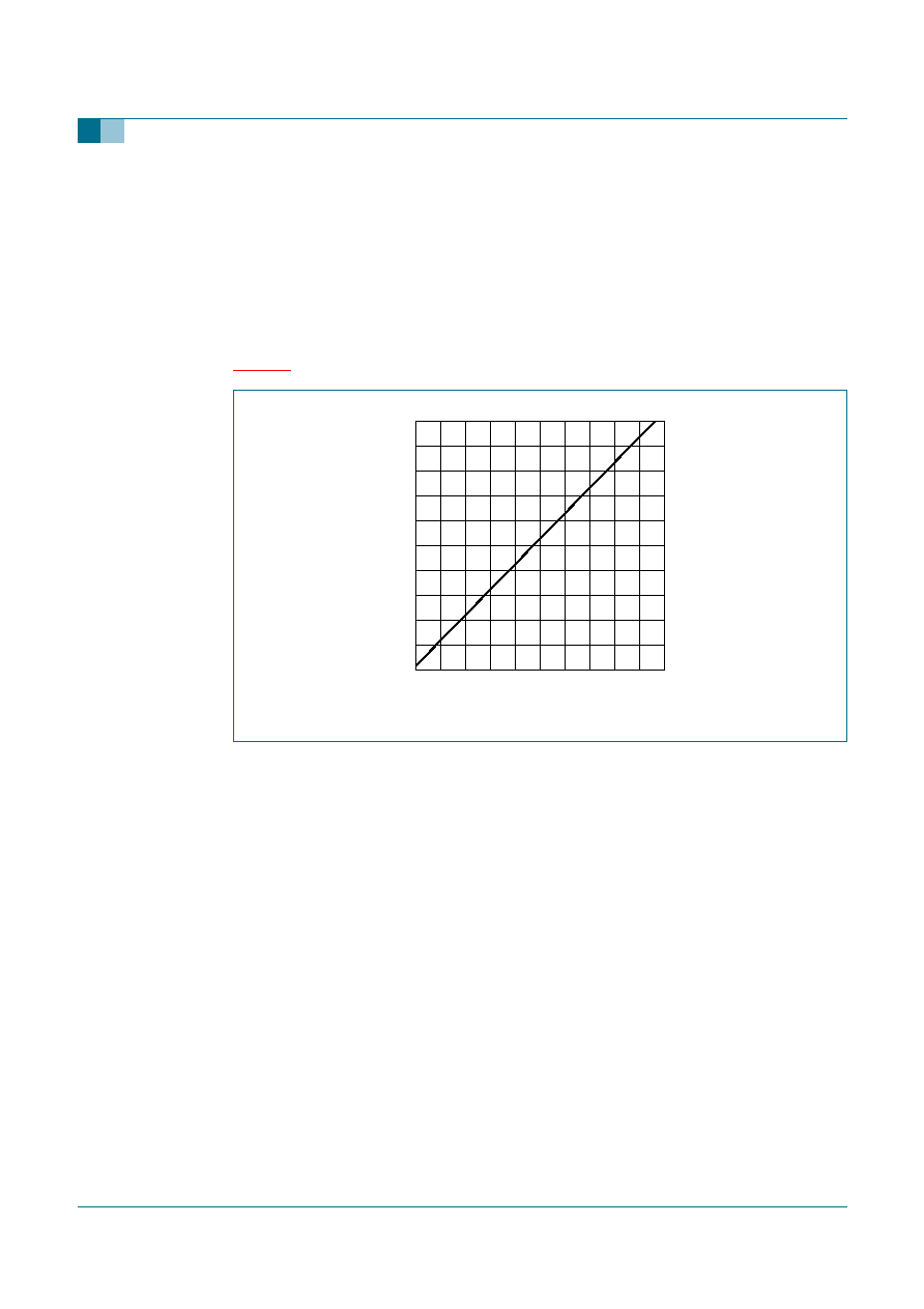
Fig 12. Maximum dissipation as a function of ambient temperature.
001aaa428
T
amb
(
�
C)
0
150
100
50
2
1
3
4
P
D
(W)
0

9397 750 12772
� Koninklijke Philips Electronics N.V. 2004. All rights reserved.
Preliminary data sheet
Rev. 01 -- 19 July 2004
15 of 24
Philips Semiconductors
SA56202
One-chip motor driver
10. Characteristics
Table 6:
Characteristics
T
amb
= 25
�
C; V
DDA
= 5 V; V
DD(SPN)
= 12 V; V
DD(SLD)
= 12 V; V
DD(ACT)
= 5 V; V
DD(LD)
= 12 V; unless otherwise specified.
Symbol
Parameter
Conditions
Min
Typ
Max
Unit
Spindle motor driver
V
DDA
system supply voltage
4.5
5.0
5.5
V
V
DD(SPN)
motor supply voltage
4.5
12
14
V
V
IO
input offset voltage Hall amplifier
-
3.5
-
+3.5
mV
V
i
input voltage range Hall amplifier
0
-
V
DDA
V
V
i(dif)(p-p)
Hall amplifier differential input
voltage (peak-to-peak value)
25
-
-
mV
V
HBIAS
voltage on pin HBIAS
I
HBIAS
= 32 mA
-
0.6
0.9
V
f
osc
oscillator frequency
R
REF
= 47 k
;
C
OSC
= 70 pF
-
18
-
MHz
f
PWM
PWM frequency
R
REF
= 47 k
;
C
OSC
= 70 pF
-
70
-
kHz
R
ds(on)
D-MOSFET on-resistance (high or
low)
-
0.35
0.50
V
VINREF
reference voltage on pin VINREF
1.2
1.65
2.5
V
V
VINSPN
torque control voltage on pin
VINSPN
0
-
V
DDA
V
Stepper motor driver
V
DDA
supply voltage
4.5
5.0
5.5
V
V
DD(SLD)
motor supply voltage
4.5
12
14
V
I
DD(SLD)
motor current limit
R
sense
= 0.5
0.85
1.0
1.15
A
f
PWM
PWM frequency
R
REF
= 47 k
;
C
OSC
= 70 pF
-
70
-
kHz
V
i(trip)
input dead-zone trip level
15
30
45
mV
g
m
transconductance gain
R
sense
= 0.5
0.85
1.0
1.15
A/V
R
ds(on)
D-MOSFET on-resistance (high or
low)
-
1.0
1.4
Loading motor driver
V
DD(LD)
motor supply voltage
4.5
12
14
V
I
DD(LD)
current limit (high or low)
0.9
1.2
2.0
A
V
OO
output offset voltage
-
100
0
+100
mV
G
v
voltage gain
16.8
17.6
18.4
dB
R
ds(on)
D-MOSFET on-resistance (high or
low)
-
0.6
0.9
Actuator driver (focus, tracking and tilt)
V
DD(ACT)
supply voltage
4.5
5
14
V
I
DD(ACT)
current limit (high or low)
0.9
1.2
2.0
A
V
OO
output offset voltage
-
55
0
+55
mV
G
v
voltage gain
16.8
17.6
18.4
dB
G
v(m)
gain mismatch between 3 channels
-
-
5
%

9397 750 12772
� Koninklijke Philips Electronics N.V. 2004. All rights reserved.
Preliminary data sheet
Rev. 01 -- 19 July 2004
16 of 24
Philips Semiconductors
SA56202
One-chip motor driver
R
ds(on)
D-MOSFET on-resistance (high or
low)
-
0.6
0.9
General
V
CP3
charge pump output voltage
-
18.2
-
V
V
IH
HIGH-level input voltage digital on
pins 26 and 27
2.0
-
-
V
V
IL
LOW-level input voltage digital on
pins 26 and 27
-
-
0.8
V
V
OL
LOW-level output voltage digital on
pins 18 and 28
I
OL
= 2 mA
-
-
0.5
V
I
DDA(q)
V
DDA
quiescent current
CTL1 = H; CTL2 = H
-
14
20
mA
I
DD(SPN)(q)
V
DD(SPN)
quiescent current
CTL1 = H; CTL2 = H
-
9
15
mA
I
DD(SLD)(q)
V
DD(SLD)
quiescent current
CTL1 = H; CTL2 = H
-
0
1
mA
I
DD(ACT)(q)
V
DD(ACT)
quiescent current
CTL1 = H; CTL2 = H
-
16
25
mA
I
STB(tot)
total standby current
CTL1 = L; CTL2 = L
-
4.5
8
mA
T
TEMP
thermal warning temperature
-
150
-
�
C
T
hys(TEMP)
thermal warning hysteresis
-
10
-
�
C
T
SD
thermal shutdown temperature
-
160
-
�
C
T
hys(SD)
thermal shutdown hysteresis
-
30
-
�
C
Table 6:
Characteristics
...continued
T
amb
= 25
�
C; V
DDA
= 5 V; V
DD(SPN)
= 12 V; V
DD(SLD)
= 12 V; V
DD(ACT)
= 5 V; V
DD(LD)
= 12 V; unless otherwise specified.
Symbol
Parameter
Conditions
Min
Typ
Max
Unit
9397 750 12772
� Koninklijke Philips Electronics N.V. 2004. All rights reserved.
Preliminary data sheet
Rev. 01 -- 19 July 2004
17 of 24
Philips Semiconductors
SA56202
One-chip motor driver
11. Application information
For R
EMF
and R
LIM
see
Section 7
.
Fig 13. Application diagram.
001aaa430
M
M
REVERSE
DETECTION
LEVEL
SHIFT
LEVEL
SHIFT
LEVEL
SHIFT
LEVEL
SHIFT
SLED
LOGIC
CURRENT
REFERENCE
FG
OSCILLATOR
THERMAL
SHUTDOWN
FG
0 V
12 V
12 V
0 V
HALL BIAS
ADC
HALL V
HALL U
HALL W
CHARGE
PUMP
MUTE/
STANDBY
FUNCTIONS
MUTE/
SELECT
SPINDLE
LOGIC
HALL
AMP
1
2
3
4
5
6
7
8
9
10
11
12
13
15
14
16
17
18
28
19
20
21
22
23
24
25
26
27
3.3 V
47 k
R
EMF
R
REF
R
LIM
47 k
3.3 V
22 nF
10 nF
5 V
1.65 V
spindle input
sled motor
spindle
motor
0 V
47 k
47 k
VINREF
VINREF
VINREF
VINREF
VINREF
VINREF
VINREF
5V
0V
150
31
30
29
33
32
34
35
36
37
38
39
40
41
42
43
44
45
46
47
48
49
50
51
52
53
54
0 V
0 V
tray motor in
focus in
tracking in
tilt in
tray
motor
focus
actuator
12 V
70 pF
12 V
0 V
sled in2
sled in1
55
56
47 k
tracking
actuator
tilt
actuator
0 V
5 V
0 V
0.5
0.5
SA56202
9397 750 12772
� Koninklijke Philips Electronics N.V. 2004. All rights reserved.
Preliminary data sheet
Rev. 01 -- 19 July 2004
18 of 24
Philips Semiconductors
SA56202
One-chip motor driver
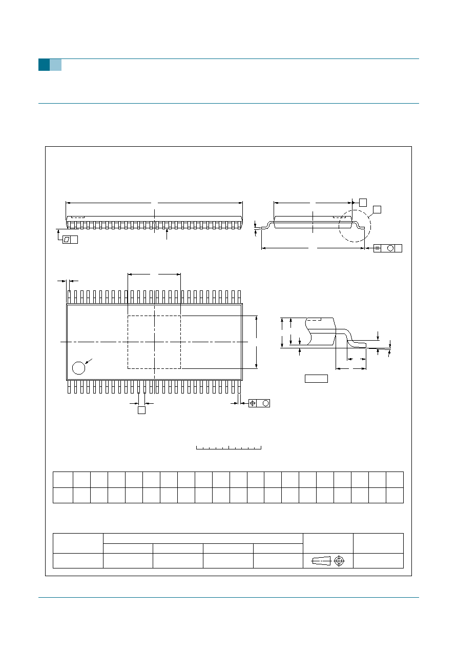
12. Package outline
Fig 14. Package outline.
UNIT
A
max.
A
1
A
2
A
3
b
p
c
e
H
E
L
L
p
y
w
v
REFERENCES
OUTLINE
VERSION
EUROPEAN
PROJECTION
ISSUE DATE
IEC
JEDEC
JEITA
mm
1.2
0.15
0.05
1.05
0.80
0.25
0.27
0.17
0.20
0.09
4.3
4.1
0.5
8.3
7.9
0.4
0.1
8
0
o
o
0.08
0.1
0.2
1
DIMENSIONS (mm are the original dimensions)
Notes
1. Plastic or metal protrusions of 0.15 mm maximum per side are not included.
2. Plastic or metal protrusions of 0.25 mm maximum per side are not included.
0.8
0.4
SOT793-1
143E36T
MO-153
03-03-04
D
(1)
14.1
13.9
E
(2)
6.2
6.0
E
h
D
h
Z
(1)
4.3
4.1
v
M
A
Eh
Dh
HE
D
E
c
X
A
Lp
detail X
L
(A3)
A2
A1
y
exposed die pad
pin 1 index
bp
w
M
HTSSOP56: plastic thermal enhanced thin shrink small outline package; 56 leads;
body width 6.1 mm; exposed die pad
SOT793-1
e
A
Z
1
56
28
29
0
2.5
5 mm
scale

9397 750 12772
� Koninklijke Philips Electronics N.V. 2004. All rights reserved.
Preliminary data sheet
Rev. 01 -- 19 July 2004
19 of 24
Philips Semiconductors
SA56202
One-chip motor driver
13. Soldering
13.1 Introduction to soldering surface mount packages
This text gives a very brief insight to a complex technology. A more in-depth account of
soldering ICs can be found in our
Data Handbook IC26; Integrated Circuit Packages
(document order number 9398 652 90011).
There is no soldering method that is ideal for all surface mount IC packages. Wave
soldering can still be used for certain surface mount ICs, but it is not suitable for fine pitch
SMDs. In these situations reflow soldering is recommended.
13.2 Reflow soldering
Reflow soldering requires solder paste (a suspension of fine solder particles, flux and
binding agent) to be applied to the printed-circuit board by screen printing, stencilling or
pressure-syringe dispensing before package placement. Driven by legislation and
environmental forces the worldwide use of lead-free solder pastes is increasing.
Several methods exist for reflowing; for example, convection or convection/infrared
heating in a conveyor type oven. Throughput times (preheating, soldering and cooling)
vary between 100 seconds and 200 seconds depending on heating method.
Typical reflow peak temperatures range from 215
�
C to 270
�
C depending on solder paste
material. The top-surface temperature of the packages should preferably be kept:
�
below 225
�
C (SnPb process) or below 245
�
C (Pb-free process)
� for all BGA, HTSSON..T and SSOP..T packages
� for packages with a thickness
2.5 mm
� for packages with a thickness < 2.5 mm and a volume
350 mm
3
so called
thick/large packages.
�
below 240
�
C (SnPb process) or below 260
�
C (Pb-free process) for packages with a
thickness < 2.5 mm and a volume < 350 mm
3
so called small/thin packages.
Moisture sensitivity precautions, as indicated on packing, must be respected at all times.
13.3 Wave soldering
Conventional single wave soldering is not recommended for surface mount devices
(SMDs) or printed-circuit boards with a high component density, as solder bridging and
non-wetting can present major problems.
To overcome these problems the double-wave soldering method was specifically
developed.
If wave soldering is used the following conditions must be observed for optimal results:
�
Use a double-wave soldering method comprising a turbulent wave with high upward
pressure followed by a smooth laminar wave.
�
For packages with leads on two sides and a pitch (e):
� larger than or equal to 1.27 mm, the footprint longitudinal axis is preferred to be
parallel to the transport direction of the printed-circuit board;

9397 750 12772
� Koninklijke Philips Electronics N.V. 2004. All rights reserved.
Preliminary data sheet
Rev. 01 -- 19 July 2004
20 of 24
Philips Semiconductors
SA56202
One-chip motor driver
� smaller than 1.27 mm, the footprint longitudinal axis must be parallel to the
transport direction of the printed-circuit board.
The footprint must incorporate solder thieves at the downstream end.
�
For packages with leads on four sides, the footprint must be placed at a 45
�
angle to
the transport direction of the printed-circuit board. The footprint must incorporate
solder thieves downstream and at the side corners.
During placement and before soldering, the package must be fixed with a droplet of
adhesive. The adhesive can be applied by screen printing, pin transfer or syringe
dispensing. The package can be soldered after the adhesive is cured.
Typical dwell time of the leads in the wave ranges from 3 seconds to 4 seconds at 250
�
C
or 265
�
C, depending on solder material applied, SnPb or Pb-free respectively.
A mildly-activated flux will eliminate the need for removal of corrosive residues in most
applications.
13.4 Manual soldering
Fix the component by first soldering two diagonally-opposite end leads. Use a low voltage
(24 V or less) soldering iron applied to the flat part of the lead. Contact time must be
limited to 10 seconds at up to 300
�
C.
When using a dedicated tool, all other leads can be soldered in one operation within
2 seconds to 5 seconds between 270
�
C and 320
�
C.
13.5 Package related soldering information
[1]
For more detailed information on the BGA packages refer to the
(LF)BGA Application Note (AN01026);
order a copy from your Philips Semiconductors sales office.
[2]
All surface mount (SMD) packages are moisture sensitive. Depending upon the moisture content, the
maximum temperature (with respect to time) and body size of the package, there is a risk that internal or
external package cracks may occur due to vaporization of the moisture in them (the so called popcorn
effect). For details, refer to the Drypack information in the
Data Handbook IC26; Integrated Circuit
Packages; Section: Packing Methods.
[3]
These transparent plastic packages are extremely sensitive to reflow soldering conditions and must on no
account be processed through more than one soldering cycle or subjected to infrared reflow soldering with
peak temperature exceeding 217
�
C
�
10
�
C measured in the atmosphere of the reflow oven. The package
body peak temperature must be kept as low as possible.
Table 7:
Suitability of surface mount IC packages for wave and reflow soldering methods
Package
[1]
Soldering method
Wave
Reflow
[2]
BGA, HTSSON..T
[3]
, LBGA, LFBGA, SQFP,
SSOP..T
[3]
, TFBGA, VFBGA, XSON
not suitable
suitable
DHVQFN, HBCC, HBGA, HLQFP, HSO, HSOP,
HSQFP, HSSON, HTQFP, HTSSOP, HVQFN,
HVSON, SMS
not suitable
[4]
suitable
PLCC
[5]
, SO, SOJ
suitable
suitable
LQFP, QFP, TQFP
not recommended
[5] [6]
suitable
SSOP, TSSOP, VSO, VSSOP
not recommended
[7]
suitable
CWQCCN..L
[8]
, PMFP
[9]
, WQCCN..L
[8]
not suitable
not suitable

9397 750 12772
� Koninklijke Philips Electronics N.V. 2004. All rights reserved.
Preliminary data sheet
Rev. 01 -- 19 July 2004
21 of 24
Philips Semiconductors
SA56202
One-chip motor driver
[4]
These packages are not suitable for wave soldering. On versions with the heatsink on the bottom side, the
solder cannot penetrate between the printed-circuit board and the heatsink. On versions with the heatsink
on the top side, the solder might be deposited on the heatsink surface.
[5]
If wave soldering is considered, then the package must be placed at a 45
�
angle to the solder wave
direction. The package footprint must incorporate solder thieves downstream and at the side corners.
[6]
Wave soldering is suitable for LQFP, QFP and TQFP packages with a pitch (e) larger than 0.8 mm; it is
definitely not suitable for packages with a pitch (e) equal to or smaller than 0.65 mm.
[7]
Wave soldering is suitable for SSOP, TSSOP, VSO and VSOP packages with a pitch (e) equal to or larger
than 0.65 mm; it is definitely not suitable for packages with a pitch (e) equal to or smaller than 0.5 mm.
[8]
Image sensor packages in principle should not be soldered. They are mounted in sockets or delivered
pre-mounted on flex foil. However, the image sensor package can be mounted by the client on a flex foil by
using a hot bar soldering process. The appropriate soldering profile can be provided on request.
[9]
Hot bar soldering or manual soldering is suitable for PMFP packages.

9397 750 12772
� Koninklijke Philips Electronics N.V. 2004. All rights reserved.
Preliminary data sheet
Rev. 01 -- 19 July 2004
22 of 24
Philips Semiconductors
SA56202
One-chip motor driver
14. Revision history
Table 8:
Revision history
Document ID
Release date
Data sheet status
Change notice
Order number
Supersedes
SA56202_1
20040719
Preliminary data sheet
-
9397 750 12772
-

Philips Semiconductors
SA56202
One-chip motor driver
9397 750 12772
� Koninklijke Philips Electronics N.V. 2004. All rights reserved.
Preliminary data sheet
Rev. 01 -- 19 July 2004
23 of 24
15. Data sheet status
[1]
Please consult the most recently issued data sheet before initiating or completing a design.
[2]
The product status of the device(s) described in this data sheet may have changed since this data sheet was published. The latest information is available on the Internet at
URL http://www.semiconductors.philips.com.
[3]
For data sheets describing multiple type numbers, the highest-level product status determines the data sheet status.
16. Definitions
Short-form specification -- The data in a short-form specification is
extracted from a full data sheet with the same type number and title. For
detailed information see the relevant data sheet or data handbook.
Limiting values definition -- Limiting values given are in accordance with
the Absolute Maximum Rating System (IEC 60134). Stress above one or
more of the limiting values may cause permanent damage to the device.
These are stress ratings only and operation of the device at these or at any
other conditions above those given in the Characteristics sections of the
specification is not implied. Exposure to limiting values for extended periods
may affect device reliability.
Application information -- Applications that are described herein for any
of these products are for illustrative purposes only. Philips Semiconductors
make no representation or warranty that such applications will be suitable for
the specified use without further testing or modification.
17. Disclaimers
Life support -- These products are not designed for use in life support
appliances, devices, or systems where malfunction of these products can
reasonably be expected to result in personal injury. Philips Semiconductors
customers using or selling these products for use in such applications do so
at their own risk and agree to fully indemnify Philips Semiconductors for any
damages resulting from such application.
Right to make changes -- Philips Semiconductors reserves the right to
make changes in the products - including circuits, standard cells, and/or
software - described or contained herein in order to improve design and/or
performance. When the product is in full production (status `Production'),
relevant changes will be communicated via a Customer Product/Process
Change Notification (CPCN). Philips Semiconductors assumes no
responsibility or liability for the use of any of these products, conveys no
license or title under any patent, copyright, or mask work right to these
products, and makes no representations or warranties that these products are
free from patent, copyright, or mask work right infringement, unless otherwise
specified.
18. Contact information
For additional information, please visit: http://www.semiconductors.philips.com
For sales office addresses, send an email to: sales.addresses@www.semiconductors.philips.com
Level
Data sheet status
[1]
Product status
[2] [3]
Definition
I
Objective data
Development
This data sheet contains data from the objective specification for product development. Philips
Semiconductors reserves the right to change the specification in any manner without notice.
II
Preliminary data
Qualification
This data sheet contains data from the preliminary specification. Supplementary data will be published
at a later date. Philips Semiconductors reserves the right to change the specification without notice, in
order to improve the design and supply the best possible product.
III
Product data
Production
This data sheet contains data from the product specification. Philips Semiconductors reserves the
right to make changes at any time in order to improve the design, manufacturing and supply. Relevant
changes will be communicated via a Customer Product/Process Change Notification (CPCN).

� Koninklijke Philips Electronics N.V. 2004
All rights are reserved. Reproduction in whole or in part is prohibited without the prior
written consent of the copyright owner. The information presented in this document does
not form part of any quotation or contract, is believed to be accurate and reliable and may
be changed without notice. No liability will be accepted by the publisher for any
consequence of its use. Publication thereof does not convey nor imply any license under
patent- or other industrial or intellectual property rights.
Date of release: 19 July 2004
Document order number: 9397 750 12772
Published in The Netherlands
Philips Semiconductors
SA56202
One-chip motor driver
19. Contents
1
General description . . . . . . . . . . . . . . . . . . . . . . 1
2
Features . . . . . . . . . . . . . . . . . . . . . . . . . . . . . . . 1
3
Applications . . . . . . . . . . . . . . . . . . . . . . . . . . . . 1
4
Ordering information . . . . . . . . . . . . . . . . . . . . . 2
5
Block diagram . . . . . . . . . . . . . . . . . . . . . . . . . . 3
6
Pinning information . . . . . . . . . . . . . . . . . . . . . . 4
6.1
Pinning . . . . . . . . . . . . . . . . . . . . . . . . . . . . . . . 4
6.2
Pin description . . . . . . . . . . . . . . . . . . . . . . . . . 4
7
Functional description . . . . . . . . . . . . . . . . . . . 6
7.1
Spindle motor control . . . . . . . . . . . . . . . . . . . . 6
7.2
Internal regeneration of back-EMF spindle
motor. . . . . . . . . . . . . . . . . . . . . . . . . . . . . . . . . 7
7.3
Sine generation using 3-phase PWM signals . . 8
7.4
Programming R
LIM
. . . . . . . . . . . . . . . . . . . . . . 9
7.5
Programming R
EMF
. . . . . . . . . . . . . . . . . . . . . 10
7.6
FG generator . . . . . . . . . . . . . . . . . . . . . . . . . 10
7.7
Sled motor driver . . . . . . . . . . . . . . . . . . . . . . 11
7.8
Loading motor driver. . . . . . . . . . . . . . . . . . . . 12
7.9
Actuator motor drivers . . . . . . . . . . . . . . . . . . 12
7.10
Charge pump . . . . . . . . . . . . . . . . . . . . . . . . . 12
7.11
Thermal protection . . . . . . . . . . . . . . . . . . . . . 12
7.12
Oscillator. . . . . . . . . . . . . . . . . . . . . . . . . . . . . 13
7.13
Muting functions . . . . . . . . . . . . . . . . . . . . . . . 13
8
Limiting values. . . . . . . . . . . . . . . . . . . . . . . . . 13
9
Thermal characteristics. . . . . . . . . . . . . . . . . . 14
10
Characteristics . . . . . . . . . . . . . . . . . . . . . . . . . 15
11
Application information. . . . . . . . . . . . . . . . . . 17
12
Package outline . . . . . . . . . . . . . . . . . . . . . . . . 18
13
Soldering . . . . . . . . . . . . . . . . . . . . . . . . . . . . . 19
13.1
Introduction to soldering surface mount
packages . . . . . . . . . . . . . . . . . . . . . . . . . . . . 19
13.2
Reflow soldering . . . . . . . . . . . . . . . . . . . . . . . 19
13.3
Wave soldering . . . . . . . . . . . . . . . . . . . . . . . . 19
13.4
Manual soldering . . . . . . . . . . . . . . . . . . . . . . 20
13.5
Package related soldering information . . . . . . 20
14
Revision history . . . . . . . . . . . . . . . . . . . . . . . . 22
15
Data sheet status . . . . . . . . . . . . . . . . . . . . . . . 23
16
Definitions . . . . . . . . . . . . . . . . . . . . . . . . . . . . 23
17
Disclaimers . . . . . . . . . . . . . . . . . . . . . . . . . . . . 23
18
Contact information . . . . . . . . . . . . . . . . . . . . 23