Document Outline
- GENERAL DESCRIPTION
- FEATURES
- SIMPLIFIED SYSTEM DIAGRAM
- APPLICATIONS
- ORDERING INFORMATION
- PIN CONFIGURATION
- PIN DESCRIPTION
- MAXIMUM RATINGS
- CHARACTERISTICS
- TYPCIAL PERFORMANCE CURVES
- PACKING METHOD
- PACKAGE
- Data sheet status
- Definitions
- Disclaimers

Philips
Semiconductors
SA57000-XX
CapFREE
TM
150 mA, low-noise, low dropout
regulator with thermal protection
Product data
Supersedes data of 2001 Jul 12
File under Integrated Circuits, Standard Analog
2001 Aug 27
INTEGRATED CIRCUITS
Philips Semiconductors
Product data
SA57000-XX
CapFREE
TM
150 mA, low-noise, low dropout regulator
with thermal protection
2
2001 Aug 27
853≠2265 26991
GENERAL DESCRIPTION
The CapFREE
TM
SA57000 is the first in a new family of unique low
dropout regulators. It needs no external capacitors, offers a low
output noise voltage of 30
µ
V
RMS
, and an ultra-low dropout voltage
of 55 mV @ 50 mA output current. To accommodate high density
layouts, it is packaged in the small footprint 5 leaded SOT23-5 (SO5).
It is ideal for all portable and cellular phone applications.
Additional features include power and thermal shutdown, output
current limitation, power OK status, thermal warning, and external
logic-controlled on-off via the PWRON pin.
FEATURES
∑
CapFREE: No output capacitor needed, stable for all capacitive
loads, regardless of ESR
∑
Low 30
µ
V
RMS
noise without noise bypass capacitor
∑
Preset output voltages to 2.5 V, 2.8 V, 3.0 V, 3.3 V and 3.6 V;
other voltages available upon request. 2% output voltage
accuracy
∑
150 mA maximum output current with current limitation
∑
Typical dropout voltage 55 mV @ 50 mA output current
∑
85
µ
A typical ground current
∑
Thermal-overload and short-circuit protection
∑
PWROK pin: both power status and thermal warning indicator
∑
PWRON pin offers logic-controlled shutdown
∑
Maximum line regulation: 0.1%/V
∑
Maximum load regulation: 0.02%/mA.
APPLICATIONS
∑
Cordless and mobile phones
∑
Industrial and medical equipment
∑
Other battery-powered equipment.
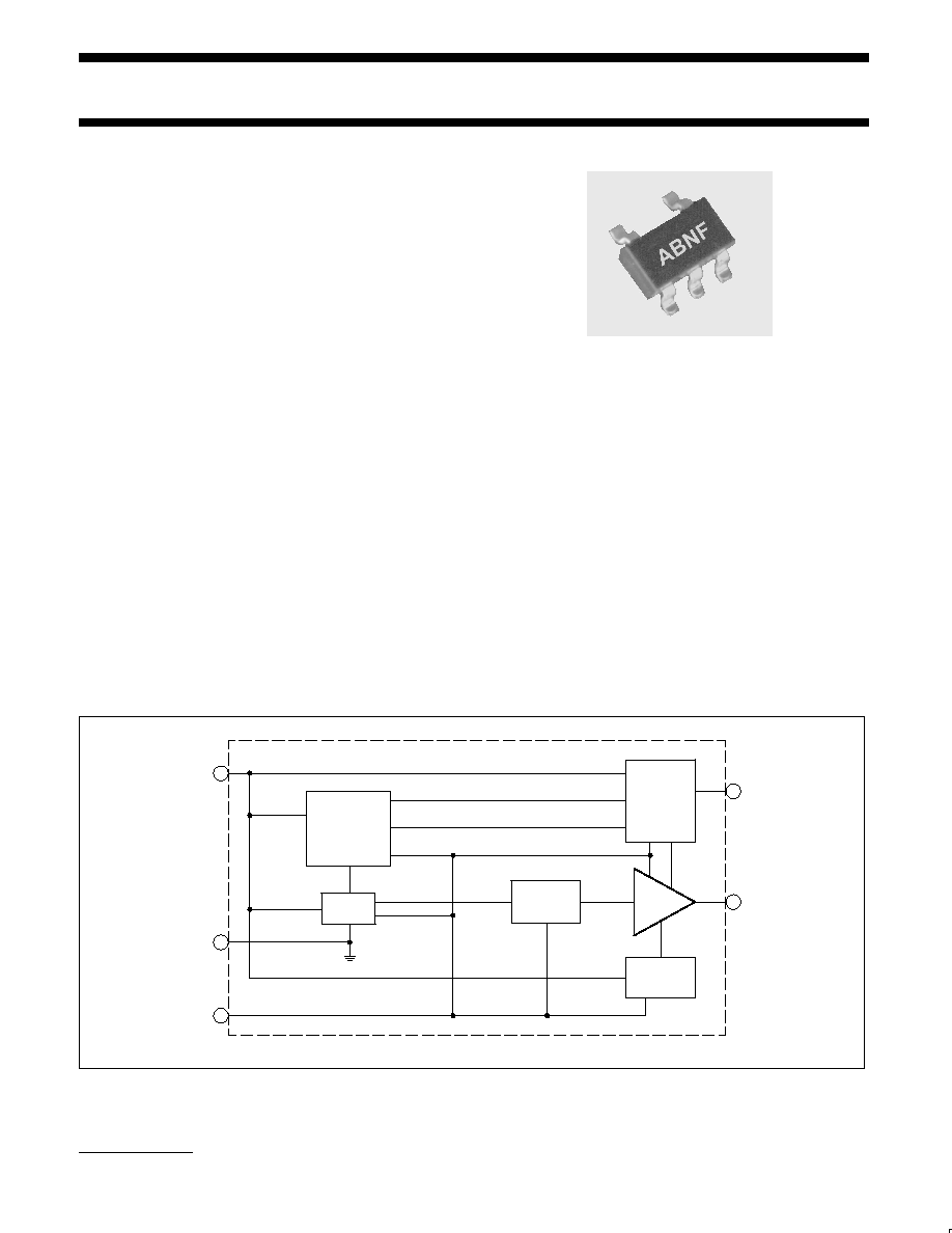
SIMPLIFIED SYSTEM DIAGRAM
SA00557
LOW-PASS
FILTER
OUTPUT
AMP.
LOGIC
CONTROL
BIAS
NETWORK
PWROK
V
OUT
PWRON
PWRON
TEMPERATURE
SENSOR
BAND
GAP
SA57000
3
PWRON
PWRON
PWRON
GND
V
IN
OVER 144
∞
C (POWER/THERMAL SHUTDOWN)
OVER 127
∞
C (POWER/THERMAL WARNING)
2
1
5
4
Figure 1. Simplified system diagram.
CapFREE is a trademark of Philips Electronics North America Corporation.
Philips Semiconductors
Product data
SA57000-XX
CapFREE
TM
150 mA, low-noise, low dropout regulator
with thermal protection
2001 Aug 27
3
ORDERING INFORMATION
TYPE NUMBER
PACKAGE
TEMPERATURE
TYPE NUMBER
NAME
DESCRIPTION
VERSION
RANGE
SA57000-XXD
SOT23-5,
SOT25, SO5
plastic small outline package; 5 leads (see dimensional drawing)
SOT680-1
≠40 to +85
∞
C
NOTE:
The device has five voltage output options, indicated by the XX on
the Type Number.
XX
VOLTAGE (Typical)
25
2.5 V
28
2.8 V
30
3.0 V
33
3.3 V
36
3.6 V
Part number marking
Each package is marked with a four letter code. The first three
letters designate the product. The fourth letter, represented by `x', is
a date tracking code.
Part number
Marking
SA57000-25D
A B K x
SA57000-28D
A B L x
SA57000-30D
A B M x
SA57000-33D
A B N x
SA57000-36D
A B P x
PIN CONFIGURATION
SA00556
1
2
3
4
5
V
OUT
PWROK
PWRON
GND
V
IN
SA57000-XX
Figure 2. Pin configuration.
PIN DESCRIPTION
PIN
SYMBOL
DESCRIPTION
1
V
IN
Regulator input. V
OUT(nom)
+ 0.1 V to 5.5 V.
No bypass capacitor required.
2
GND
Ground.
3
PWRON
Power-on input. Active-HIGH. A logic LOW
powers down regulator. The shutdown
quiescent current is typically 50 nA.
Connect to V
IN
for manual operation.
4
PWROK
Power OK indicator, including thermal
warning. Trips (goes LOW) at 127
∞
C (
±
2
∞
),
or when power falls typically 6% below
V
OUT(nom)
.
5
V
OUT
Regulator output. Sources up to 150 mA.
No bypass capacitors required.
MAXIMUM RATINGS
SYMBOL
PARAMETER
MIN.
MAX.
UNIT
V
IN
V
IN
to GND voltage
≠0.3
5.5
V
dc
V
PWRON
PWRON to GND voltage
≠0.3
5.5
V
dc
V
OUT
OUT to GND voltage
≠0.3
V
IN
+ 0.3
V
dc
T
amb
Operating ambient temperature
≠40
+85
∞
C
T
j
Junction temperature
≠
+150
∞
C
T
stg
Storage temperature
≠65
+160
∞
C
P
Power dissipation
≠
575
mW
R
th(j-a)
Thermal resistance from junction to ambient
≠
140
∞
C/W

Philips Semiconductors
Product data
SA57000-XX
CapFREE
TM
150 mA, low-noise, low dropout regulator
with thermal protection
2001 Aug 27
4
CHARACTERISTICS
V
IN
= V
OUT(nom)
+ 0.5 V. (Note 1.)
SYMBOL
PARAMETER
CONDITIONS
MIN.
TYP.
MAX.
UNIT
V
IN
input voltage
V
OUT(nom)
≠
5.5
V
output voltage accuracy
2
I
OUT
= 1 mA
T
amb
= +25
∞
C
≠
±
1
≠
%
≠40
∞
C
T
amb
+85
∞
C
≠2.0
≠
2.0
%
I
LIM
current limit
160
300
≠
mA
I
Q
ground pin current
I
OUT
= 1 mA to 150 mA
≠
85
150
µ
A
dropout voltage
3
I
OUT
= 1 mA
≠
1
≠
mV
I
OUT
= 50 mA
≠
55
120
mV
I
OUT
= 150 mA
≠
165
≠
mV
V
LNR
line regulation
V
IN
= (V
OUT
+ 0.1 V) to 5.5 V; I
OUT
= 20 mA
≠
≠
0.1
%/V
V
LDR
load regulation
I
OUT
= 1 mA to 150 mA
≠
0.01
0.02
%/mA
e
n
output voltage noise
f = 10 Hz to 100 kHz, C
OUT
= 10
µ
F
≠
30
≠
µ
V
RMS
Shutdown
V
IH
PWRON input threshold
(HIGH ON-state)
V
IN
V
OUT(nom)
5.5 V
0.7
◊
V
IN
≠
≠
V
V
IL
PWRON input threshold
(HIGH ON-state)
V
IN
V
OUT(nom)
5.5 V
≠
≠
0.3
◊
V
IN
V
I
PWRON
PWRON input bias current
V
PWRON
= V
IN
T
amb
= +25
∞
C
≠
0.01
1
µ
A
T
amb
= +85
∞
C
≠
0.05
≠
µ
A
I
Q(SHDN)
shutdown supply current
V
OUT
= 0 V
T
amb
= +25
∞
C
≠
0.05
1
µ
A
T
amb
= +85
∞
C
≠
0.2
1
µ
A
t
PWRON
power-on start-up time
4
I
OUT
= 1 mA, C
OUT
= 100 nF
T
amb
= +25
∞
C
≠
25
100
µ
s
T
amb
= ≠40 to +85
∞
C
≠
35
200
µ
s
Thermal protection (Note 2)
T
SHDN
thermal shut-down temperature
≠
144
≠
∞
C
T
SHDN
thermal shut-down hysteresis
≠
13
≠
∞
C
PWROK output (power and temperature OK) (Note 2)
PWROK trip temperature
≠
127
≠
∞
C
PWROK trip temperature
hysteresis
≠
12
≠
∞
C
PWROK trip as percentage of
V
OUT(nom)
≠3.5
≠6
≠8
%
PWROK hysteresis as
percentage of V
OUT(nom)
≠
2
≠
%
PWROK output (when tripped)
I
SINK
= 0.5 mA
≠
0.1
0.4
V
NOTES:
1. Limits are production tested at T
amb
= +25
∞
C. All devices are 100% production tested at 25
∞
C. Limits over the operating tempreature are
guaranteed by design.
2. Accuracy
±
2
∞
C over temperature range guaranteed by design and characterization.
3. The dropout voltage is defined as V
IN
≠ V
OUT
,
where V
OUT
is 100 mV below the value of V
OUT
for V
IN
= V
OUT
+ 0.5 V..
4. Time needed for V
OUT
to reach 95% of V
OUT(nom)
.
Philips Semiconductors
Product data
SA57000-XX
CapFREE
TM
150 mA, low-noise, low dropout regulator
with thermal protection
2001 Aug 27
5
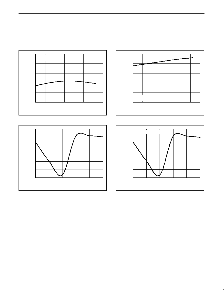
TYPCIAL PERFORMANCE CURVES
Measurements taken with the SA57000-33 (3.3 volt output).
SL01515
T
amb
, TEMPERATURE
∞
C)
V
OUT
, OUTPUT
VOL
T
AGE
(V)
≠40
≠20
0
20
40
60
80
100
3.40
3.38
3.36
3.34
3.32
3.30
I
LOAD
= 50 mA
V
IN
= V
OUT(nom)
+ 0.5 V
Figure 3. Output voltage versus temperature.
T
amb
, TEMPERATURE
∞
C)
GROUND
CURRENT
(
A)
µ
≠40
≠20
0
20
40
60
80
100
100
80
60
40
20
0
V
IN
= V
OUT(nom)
+ 0.5 V
I
LOAD
= 50 mA
SL01516
Figure 4. Ground current versus temperature.
SL01517
V
IN
, INPUT VOLTAGE (V)
GROUND
CURRENT
(
A)
µ
1.0
2.0
3.0
4.0
5.0
6.0
0
≠100
≠300
≠400
≠500
≠600
≠200
Figure 5. Ground current versus input voltage (no load).
SL01518
V
IN
, INPUT VOLTAGE (V)
GROUND
CURRENT
(
A)
µ
1.0
2.0
3.0
4.0
5.0
6.0
0
≠100
≠300
≠400
≠500
≠600
≠200
LOAD CURRENT = 50 mA
Figure 6. Ground current versus input voltage with load.
Philips Semiconductors
Product data
SA57000-XX
CapFREE
TM
150 mA, low-noise, low dropout regulator
with thermal protection
2001 Aug 27
6
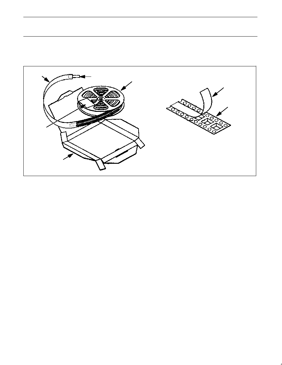
PACKING METHOD
The SA57000-XX is packed in reels, as shown in Figure 7.
SL01305
TAPE DETAIL
COVER TAPE
CARRIER TAPE
REEL
ASSEMBLY
TAPE
GUARD
BAND
BARCODE
LABEL
BOX
Figure 7. Tape and reel packing method

Philips Semiconductors
Product data
SA57000-XX
CapFREE
TM
150 mA, low-noise, low dropout regulator
with thermal protection
2001 Aug 27
7
SO5:
plastic small outline package; 5 leads; body width 1.6 mm
SOT680-1
Philips Semiconductors
Product data
SA57000-XX
CapFREE
TM
150 mA, low-noise, low dropout regulator
with thermal protection
2001 Aug 27
8
Definitions
Short-form specification -- The data in a short-form specification is extracted from a full data sheet with the same type number and title. For
detailed information see the relevant data sheet or data handbook.
Limiting values definition -- Limiting values given are in accordance with the Absolute Maximum Rating System (IEC 60134). Stress above one
or more of the limiting values may cause permanent damage to the device. These are stress ratings only and operation of the device at these or
at any other conditions above those given in the Characteristics sections of the specification is not implied. Exposure to limiting values for extended
periods may affect device reliability.
Application information -- Applications that are described herein for any of these products are for illustrative purposes only. Philips
Semiconductors make no representation or warranty that such applications will be suitable for the specified use without further testing or
modification.
Disclaimers
Life support -- These products are not designed for use in life support appliances, devices or systems where malfunction of these products can
reasonably be expected to result in personal injury. Philips Semiconductors customers using or selling these products for use in such applications
do so at their own risk and agree to fully indemnify Philips Semiconductors for any damages resulting from such application.
Right to make changes -- Philips Semiconductors reserves the right to make changes, without notice, in the products, including circuits, standard
cells, and/or software, described or contained herein in order to improve design and/or performance. Philips Semiconductors assumes no
responsibility or liability for the use of any of these products, conveys no license or title under any patent, copyright, or mask work right to these
products, and makes no representations or warranties that these products are free from patent, copyright, or mask work right infringement, unless
otherwise specified.
Contact information
For additional information please visit
http://www.semiconductors.philips.com.
Fax: +31 40 27 24825
For sales offices addresses send e-mail to:
sales.addresses@www.semiconductors.philips.com.
©
Koninklijke Philips Electronics N.V. 2001
All rights reserved. Printed in U.S.A.
Date of release: 08-01
Document order number:
9397 750 08722
Philips
Semiconductors
Data sheet status
[1]
Objective data
Preliminary data
Product data
Product
status
[2]
Development
Qualification
Production
Definitions
This data sheet contains data from the objective specification for product development.
Philips Semiconductors reserves the right to change the specification in any manner without notice.
This data sheet contains data from the preliminary specification. Supplementary data will be
published at a later date. Philips Semiconductors reserves the right to change the specification
without notice, in order to improve the design and supply the best possible product.
This data sheet contains data from the product specification. Philips Semiconductors reserves the
right to make changes at any time in order to improve the design, manufacturing and supply.
Changes will be communicated according to the Customer Product/Process Change Notification
(CPCN) procedure SNW-SQ-650A.
Data sheet status
[1] Please consult the most recently issued data sheet before initiating or completing a design.
[2] The product status of the device(s) described in this data sheet may have changed since this data sheet was published. The latest information is available on the Internet at URL
http://www.semiconductors.philips.com.