 | –≠–ª–µ–∫—Ç—Ä–æ–Ω–Ω—ã–π –∫–æ–º–ø–æ–Ω–µ–Ω—Ç: SA57001 | –°–∫–∞—á–∞—Ç—å:  PDF PDF  ZIP ZIP |
Document Outline
- GENERAL DESCRIPTION
- FEATURES
- APPLICATIONS
- SIMPLIFIED SYSTEM DIAGRAM
- ORDERING INFORMATION
- PIN CONFIGURATION
- PIN DESCRIPTION
- MAXIMUM RATINGS
- ELECTRICAL CHARACTERISTICS
- SMBus INTERFACE AC ELECTRICAL CHARACTERISTICS
- TECHNICAL DESCRIPTION
- FUNCTIONAL DESCRIPTION
- INTERRUPTION LOGIC FUNCTIONAL DESCRIPTION A B,C D E, F
- SMBus INTERFACE
- PACKING METHOD
- PACKAGE OUTLINE
- REVISION HISTORY
- Data sheet status
- Definitions
- Disclaimers

Philips
Semiconductors
SA56004X
±
1
∞
C accurate, SMBus-compatible, 8-pin,
remote/local digital temperature sensor
with over temperature alarms
Objective data
Replaces SA56004≠X dated 2003 Aug 19
2003 Sep 03
INTEGRATED CIRCUITS
Philips Semiconductors
Objective data
SA56004X
±
1
∞
C accurate, SMBus-compatible, 8-pin, remote/local
digital temperature sensor with over temperature alarms
2
2003 Sep 03
GENERAL DESCRIPTION
The Philips SA56004X is an SMBus compatible, 11-bit remote/local
digital temperature sensor with over temperature alarms. The
remote channel of the SA56004 monitors a diode junction, such as a
substrate PNP of a microprocessor or a diode connected transistor
such as the 2N3904 (NPN) or 2N3906 (PNP). With factory trimming,
remote sensor accuracy of
±
1
∞
C is achieved.
Under and over temperature alert thresholds can be programmed to
cause the ALERT output to indicate when the on-chip or remote
temperature is out of range. This output may be used as a system
interrupt or SMBus alert. The T_CRIT output is activated when the
on-chip or remote temperature measurement rises above the
programmed T_CRIT threshold register value. This output may be
used to activate a cooling fan, send a warning or trigger a system
shutdown. To further enhance system reliability, the SA56004X
employs an SMBus time-out protocol. The SA56004X has a unique
device architecture which is patented (U.S. patent #6542020).
The SA56004X is available in the SO8 and TSSOP8 packages.
SA56004X has 8 factory-programmed, device address options.
The SA56004X is pin-compatible with the LM86, MAX6657/8, and
ADM1032.
Patents
Notice is herewith given that the subject device uses one or more of
the following patents and that each of these patents may have
corresponding patents in other jurisdictions:
Patent No. US 6,542,020 B2 -- owned by Koninklijke Philips
Electronics N.V., Eindhoven (NL).
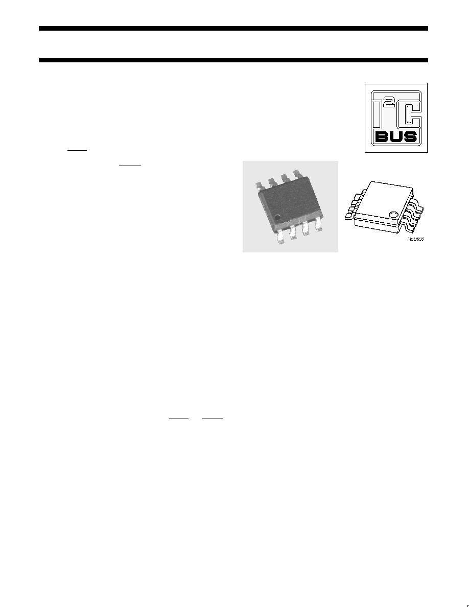
SO8
TSSOP8
FEATURES
∑
Accurately senses temperature of remote microprocessor thermal
diodes or diode connected transistors within
±
1
∞
C
∑
On-chip local temperature sensing
∑
11-bit, 0.125
∞
C resolution
∑
8 different device addresses are available for server applications.
The SA56004ED/EDP which marking code ARW is address
compatible with the National LM86, the MAX6657/8 and the
ADM1032.
∑
Offset registers available for adjusting the remote temperature
accuracy
∑
Programmable under/overtemperature alarms: ALERT and T_CRIT
∑
SMBus 2.0 compatible interface, supports TIMEOUT
∑
I
2
C-bus standard and fast mode compatible
∑
TSSOP8 and SO8 packages
∑
Programmable conversion rate (0.0625 to 26 Hz)
∑
Undervoltage lockout prevents erroneous temperature readings
APPLICATIONS
∑
System thermal management in laptops, desktops, servers and
workstations
∑
Computers and office electronic equipment
∑
Electronic test equipment & instrumentation
∑
HVAC
∑
Industrial controllers and embedded systems

Philips Semiconductors
Objective data
SA56004X
±
1
∞
C accurate, SMBus-compatible, 8-pin, remote/local
digital temperature sensor with over temperature alarms
2003 Sep 03
3
SIMPLIFIED SYSTEM DIAGRAM
SL02018
1
2
3
4
8
7
6
5
V
DD
D+
D≠
T_CRIT
SCLK
SDATA
ALERT
GND
SA56004X
R
10 k
R
10 k
R
10 k
SMBus
CONTROLLER
GND
CLOCK
DATA
INT
V
DD
V
DD
SHIELDED TWISTED PAIR
REMOTE
SENSOR
FAN CONTROL
CIRCUIT
+5 V
100 nF
2.2 nF
R
10 k
V
DD
Figure 1. Simplified system diagram.
ORDERING INFORMATION
TYPE NUMBER
PACKAGE
VERSION
TEMPERATURE
TYPE NUMBER
NAME
DESCRIPTION
VERSION
RANGE
SA56004XD
SO8
plastic small outline package; 8 leads; body width 3.9 mm
SOT96-1
0
∞
C to +125
∞
C
SA56004XDP
TSSOP8
plastic thin shrink small outline package; 8 leads; body width 3 mm
SOT505-1
0
∞
C to +125
∞
C
NOTE:
There are 8 device slave address options (indicated by `X' in the Type Number, and described in Table 1).
Table 1. Device slave address options
Part number
Device slave address
1
Part number
Device slave address
1
SA56004AD
SA56004ADP
1001000
SA56004ED
2
SA56004EDP
2
1001100
SA56004BD
SA56004BDP
1001001
SA56004FD
SA56004FDP
1001101
SA56004CD
SA56004CDP
1001010
SA56004GD
SA56004GDP
1001110
SA56004DD
SA56004DDP
1001011
SA56004HD
SA56004HDP
1001111
NOTES:
1. The device slave address is factory-programmed in OTP device address register.
2. The SA56004ED/EDP has the bus address of the National LM86, MAX6657/8 and the ADM1032.

Philips Semiconductors
Objective data
SA56004X
±
1
∞
C accurate, SMBus-compatible, 8-pin, remote/local
digital temperature sensor with over temperature alarms
2003 Sep 03
4
PIN CONFIGURATION
SO8 and TSSOP8
SL02014
1
2
3
4
8
7
6
5
TOP VIEW
V
DD
D+
D≠
T_CRIT
SCLK
SDATA
ALERT
GND
SA56004X
Figure 2. Pin configuration.
PIN DESCRIPTION
PIN
SYMBOL
DESCRIPTION
1
V
DD
Positive supply voltage. DC voltage from 3.0 V
to 5.5 V.
2
D+
Diode current source (anode).
3
D≠
Diode sink current (cathode).
4
T_CRIT
T_CRIT alarm is open drain, active-LOW output
which requires an external pull-up resistor. It
functions as a system interrupt or power
shutdown.
5
GND
Power supply ground.
6
ALERT
ALERT alarm is an open drain, active-LOW
output which requires an external pull-up resistor.
It functions as an interrupt indicating that the
temperature of the on-chip or remote diode is
above or below programmed over temperature
or under temperature thresholds.
7
SDATA
SMBus/I
2
C-bus bi-directional data line. This is
an open drain output which requires an external
pull-up resistor.
8
SCLK
SMBus/I
2
C-bus clock input which requires an
external pull-up resistor.
MAXIMUM RATINGS
All voltages are referenced to GND.
SYMBOL
PARAMETER
MIN.
MAX.
UNIT
V
DD
Supply voltage
≠0.3
+6
V
Voltage at SDATA, SCLK, ALERT, T_CRIT
≠0.3
+6
V
V
D+
Voltage at Positive diode input
≠0.3
V
DD
+ 0.3
V
V
D≠
Voltage at Negative diode input
≠0.3
+0.8
V
Sink current at SDATA, SCLK, ALERT, T_CRIT
≠1
50
mA
I
D+
D+ input current
≠1
1
mA
P
D
Power dissipation
SO8 package (derate 5.9 mW/
∞
C above T
amb
= 70
∞
C)
≠
471
mW
TSSOP8 package (derate 8.3 mW/
∞
C above T
amb
= 70
∞
C)
≠
664
mW
T
j(max)
Maximum junction temperature
≠
+150
∞
C
T
stg
Storage temperature range
≠65
+165
∞
C
Philips Semiconductors
Objective data
SA56004X
±
1
∞
C accurate, SMBus-compatible, 8-pin, remote/local
digital temperature sensor with over temperature alarms
2003 Sep 03
5
ELECTRICAL CHARACTERISTICS
T
amb
= 25
∞
C, V
DD
= 3.0 V to 3.6 V, unless otherwise specified.
SYMBOL
PARAMETER
CONDITIONS
MIN.
TYP.
MAX.
UNIT
T
ERRL
Local temperature error
T
amb
= 60
∞
C to +100
∞
C
≠2
±
1
+2
∞
C
T
amb
= 0
∞
C to +125
∞
C
≠3
≠
+3
∞
C
T
ERRR
Remote temperature error
T
amb
= +25
∞
C to +85
∞
C; T
RD
= +60
∞
C to +100
∞
C
≠1
≠
+1
∞
C
T
amb
= 0
∞
C to +85
∞
C; T
RD
= 0
∞
C to +125
∞
C
≠3
≠
+3
∞
C
T
RESR
Remote temperature resolution
≠
11
≠
bits
≠
0.125
≠
∞
C
T
RESL
Local temperature resolution
≠
11
≠
bits
≠
0.125
≠
∞
C
t
CONV
Conversion time
≠
38
≠
ms
V
DD
Supply voltage
1
3.0
≠
5.5
V
I
DD
Quiescent current
During conversion, 26 Hz conversion rate
≠
500
≠
µ
A
Shutdown current
SMBus inactive
≠
10
≠
µ
A
I
RD
Remote diode source current
High setting: D+ ≠ D≠ = +0.65 V
≠
160
≠
µ
A
Low setting
≠
10
≠
µ
A
UVL
Undervoltage lockout (UVL)
threshold voltage
2
V
DD
input disables A/D conversion
3
2.6
≠
2.95
V
Power-on-Reset (POR) threshold
voltage
V
DD
, input falling edge
4
1.8
≠
2.4
V
Local and Remote ALERT HIGH
default temperature settings
Default values set at power-up
≠
+70
≠
∞
C
Local and Remote ALERT LOW
default temperature settings
Default values set at power-up
≠
0
≠
∞
C
Local and Remote T_CRIT
default temperature settings
Default values set at power-up
≠
+85
≠
∞
C
Hystersis (T_CRIT)
Default value set at power-up
≠
+10
≠
∞
C
ALERT and T_CRIT output
saturation voltage
I
OUT
= 6.0 mA
≠
≠
0.4
V
NOTES:
1. The SA56004X is optimized for 3.3 V
DD
operation.
2. Definition of Under Voltage Lockout (UVL): The value of V
DD
below which the internal A/D converter is disabled. This is designed to be a
minimum of 200 mV above the power-on-reset. During the time that it is disabled, the temperature that is in the "read temperature registers"
will remain at the value that it was before the A/D was disabled. This is done to eliminate the possibility of reading unexpected false
temperatures due to the A/D converter not working correctly due to low voltage. In case of power-up (rising V
DD
), the reading that is stored
in the "read temperature registers" will be the default value of 0
∞
C. V
DD
will rise to the value of the UVL, at which point the A/D will function
correctly and the normal temperature will be read.
3. V
DD
(rising edge) voltage below which the A/D converter is disabled.
4. V
DD
(falling edge) voltage below which the logic is reset.
Philips Semiconductors
Objective data
SA56004X
±
1
∞
C accurate, SMBus-compatible, 8-pin, remote/local
digital temperature sensor with over temperature alarms
2003 Sep 03
6
SMBus INTERFACE AC ELECTRICAL CHARACTERISTICS
V
DD
= 3.0 V to 3.6 V; T
amb
= 0
∞
C to +125
∞
C; unless otherwise noted.
These specifications are guaranteed by design and not tested in production.
SYMBOL
PARAMETER
CONDITIONS
MIN.
TYP.
MAX.
UNIT
V
IH
Logic input HIGH voltage for SCLK, SDATA
V
DD
= 2.7 V to 5.5 V
2.2
≠
≠
V
V
IL
Logic input LOW voltage for SCLK, SDATA
V
DD
= 2.7 V to 5.5 V
≠
≠
0.8
V
I
OL
Logic output LOW sink current
ALERT, T_CRIT; V
OL
= 0.4 V
1.0
≠
≠
mA
SDATA; V
OL
= 0.6 V
6.0
≠
≠
mA
I
OH
Logic output high leakage current
V
OH
= V
DD
≠
≠
1.0
µ
A
I
IH
, I
IL
Logic input currents
V
IN
= V
DD
or GND
≠1.0
≠
1.0
µ
A
C
i
SMBus input capacitance for SCLK, SDATA
≠
5
≠
pF
SMBus digital switching characteristics
The switching characteristics of the SA56004X fully meet or exceed all parameters specified in SMBus version 2.0. The following parameters
specify the timing between the SCLK and SDATA signals in the SA56004X. They adhere to, but are not necessarily specified as the SMBus
specifications.
f
SCLK
SCLK operating frequency
≠
≠
400
kHz
t
LOW
SCLK LOW time
10% to 10%
4.7
5.0
≠
µ
s
t
HIGH
SCLK HIGH time
90% to 90%
4.0
5.0
≠
µ
s
t
BUF
SMBus free time.
Delay from SDATA stop to SDATA start
4.7
≠
≠
µ
s
t
HD:STA
Hold time of start condition.
Delay from SDATA start to first SCLK H-L
10% of SDATA to 90% of SCLK
4.0
≠
≠
µ
s
t
HD:DAT
Hold time of data.
Delay from SCLK H-L to SDATA edges
≠
300
≠
ns
t
SU:DAT
Set-up time of data in.
Delay from SDATA edges to SCLK L-H
250
≠
≠
ns
t
SU:STA
Set-up time of repeat start condition.
Delay from SCLK L-H to restart SDATA
90% to to 90%
250
≠
≠
ns
t
SU:STO
Set-up time of stop condition.
Delay from SCLK H-L to SDATA stop
90% of SCLK to 90% of SDATA
4.0
≠
≠
µ
s
t
R
Rise time of SCLK and SDATA
≠
≠
1
µ
s
t
F
Fall time of SCLK and SDATA
≠
≠
300
ns
t
OF
Output fall time
C
L
= 400 pF; I
O
= 3 mA
≠
≠
250
ns
t
TIMEOUT
SMBus TIMEOUT.
Low period for reset of SMBus
25
≠
35
ms
t
BUF
P
S
SCLK
SDATA
SL01204
t
HD:STA
S
P
t
LOW
t
R
t
F
t
HD:STA
t
HD:DAT
t
HIGH
t
SU:DAT
t
SU:STA
t
SU:STO
Figure 3. Timing measurements.
Philips Semiconductors
Objective data
SA56004X
±
1
∞
C accurate, SMBus-compatible, 8-pin, remote/local
digital temperature sensor with over temperature alarms
2003 Sep 03
7
TECHNICAL DESCRIPTION
General discussion
SMBus INTERFACE
11-BIT
≠
A≠to≠D
CONVERTER
LOCAL
TEMP
SENSOR
LOCAL
REMOTE
MUX
ONE-SHOT
REGISTER
CONVERSION
REGISTER
LOCAL TEMP
DATA REGISTER
REMOTE TEMP
DATA REGISTER
CONFIGURATION
REGISTER
LOCAL HIGH TEMP
THRESHOLD
LOCAL LOW TEMP
THRESHOLD
REMOTE HIGH
TEMP THRESHOLD
LOCAL TEMP HIGH
LIMIT REG
LOCAL TEMP LOW
LIMIT REGISTER
REMOTE TEMP
HIGH LIMIT REG
REMOTE TEMP
LOW LIMIT REG
REMOTE LOW
TEMP THRESHOLD
STATUS REGISTER
T_CRIT
INTERRUPT
COMMAND
REGISTER
ALERT
IINTERRUPT
OTP DEVICE
ADDRESS REGISTER
V
DD
D+
D≠
ALERT
T_CRIT
GND
SDATA
SCLK
REMOTE OFFSET
REGISTER
CONTROL
LOGIC
SL02015
T_CRIT
HYSTERESIS
SA56004X
Figure 4. Functional diagram.
FUNCTIONAL DESCRIPTION
Serial bus interface
The SA56004X should be connected to a compatible two-wire serial
interface System Management Bus (SMBus) as a slave device
using the two device terminals SCLK and SDATA. The ALERT pin
can optionally be used with the SMBus protocol to implement the
ARA response. The controller will provide a clock signal to the
device SCLK pin and write/read data to/from the device through the
device SDATA pin. External pull-up resistors, about 10 k
each, are
needed for these device pins due to open drain circuitry.
Data of 8-bit digital byte or word are used for communication
between the controller and the device using SMBus 2.0 protocols
which are described more in the `SMBus Interface' section on
page 14. The operation of the device to the bus is described with
details in the following sections.
Slave address
The SA56004X has a 7-bit slave address register which is factory
programmed in OTP memory. Eight unique devices are available
with different slave addresses as defined in the `Ordering
information' section in Table 1, `Device slave address options'. Up to
eight devices can reside on the same SMBus without conflict,
provided that their addresses are unique.
Register overview
The SA56004X contains three types of SMBus addressable registers.
These are read only (R), write only (W), and read-write (R/W).
Attempting to write to any R-only register or read data from any
W-only register will produce an invalid result. Some of the R/W
registers have separate addresses for reading and writing operations.
The registers of the SA56004X serve four purposes:
∑
Control and configuration of the SA56004X
∑
Status reporting
∑
Temperature measurement storage
∑
ID and manufacturer test registers.
Table 2 describes the names, addresses, power-on-reset (POR),
and functions of each register. The data of the temperature-related
registers is in 2's complement format in which the MSB is the sign
bit. The 8-bit data of other registers is in 8-bit straight format.
Philips Semiconductors
Objective data
SA56004X
±
1
∞
C accurate, SMBus-compatible, 8-pin, remote/local
digital temperature sensor with over temperature alarms
2003 Sep 03
8
Table 2. Register assignments
REGISTER
NAME
COMMAND BYTE
POR
STATE
FUNCTION
BITS
ACCESSIBILITY
NAME
READ
ADDRESS
WRITE
ADDRESS
STATE
LTHB
00h
NA
0000 0000
Local Temperature HIGH Byte
8
R
RTHB
01h
NA
0000 0000
Remote Temperature HIGH Byte
8
R
SR
02h
NA
0000 0000
Status Register
8
R
CON
03h
09h
0000 0000
Configuration Register
8
R/W
CR
04h
0Ah
1000
Conversion Rate
4
R/W
LHS
05h
0Bh
0100 0110
Local HIGH Setpoint
8
R/W
LLS
06h
0Ch
0000 0000
Local LOW Setpoint
8
R/W
RHSHB
07h
0Dh
0100 0110
Remote HIGH Setpoint High Byte
8
R/W
RLSHB
08h
0Eh
0000 0000
Remote LOW Setpoint High Byte
8
R/W
One Shot
NA
0Fh
Writing register initiate a one shot conversion
0
W
RTLB
10h
NA
0000 00
Remote Temperature LOW Byte
6(MSBs)
R
RTOHB
11h
11h
0000 0000
Remote Temperature Offset High Byte
8
R/W
RTOLB
12h
12h
000
Remote Temperature Offset Low Byte
3(MSBs)
R/W
RHSLB
13h
13h
000
Remote HIGH Setpoint Low Byte
3(MSBs)
R/W
RLSLB
14h
14h
000
Remote LOW Setpoint Low Byte
3(MSBs)
R/W
RCS
19h
19h
0101 0101
Remote T_CRIT Setpoint
8
R/W
LCS
20h
20h
0101 0101
RLocal T_CRIT Setpoint
8
R/W
TH
21h
21h
0 1010
T_CRIT Hysteresis
5
R/W
LTLB
22h
NA
0000 0000
Local Temperature Low Byte
3(MSBs)
R
AM
BFh
BFh
0
Alert Mode
1
R/W
RMID
FEh
NA
1010 0001
Read Manufacturer's ID
8
R
RDR
FFh
NA
0000 0000
Read Stepping or Die Revision
8
R
Power-on-reset (POR)
When power is applied to the SA56004X, the device will enter into
its power-on-reset state and its registers are reset to their default
values. The configuration, status, and temperature-reading registers
remain in these states until after the first conversion. As shown in
Table 2, this results in:
1. Command register set to 00h.
2. Local Temperature register (LTHB and LTLB) set to 0
∞
C.
3. Remote Diode Temperature register (RTHB and RTLB) set to
0
∞
C until the end of the first conversion.
4. Status register (SR) set to 00h.
5. Configuration register (CON) set to 00h; Interrupt latches are
cleared, the ALERT and T_CRIT output drivers are off and the
ALERT and T_CRIT pins are pulled HIGH by the external pull-up
resistors.
6. Local T_CRIT temperature setpoints (LCS) and Remote T_CRIT
temperature setpoints (RCS) at 85
∞
C.
7. Local HIGH setpoint (LHS) and remote HIGH temperature
setpoint (RHSHB) at 70
∞
C.
8. Local LOW setpoint (LLS) and Remote LOW temperature
setpoints (RLSHB) at 0
∞
C.
9. Conversion Rate register (CR) is set to 8h; the default value of
about 16 conversions/s.
Starting conversion
Upon POR, the RUN/STOP bit 6 of the configuration register is zero
(default condition), then, the device will enter into its free-running
operation mode in which the device A/D converter is enabled and
the measurement function is activated. In this mode, the device
cycles the measurements of the local and remote temperature
automatically and periodically. The conversion rate is defined by the
programmable conversion rate stored in the conversion rate register.
It also performs comparison between readings and limits of the
temperature in order to set the flags and interruption accordingly at
the end of every conversion. Measured values are stored in the
temp registers, results of the limit comparisons are reflected by the
status of the flag bits in the status register and the interruption is
reflected by the logical level of the ALERT and T_CRIT output. If the
power-on temperature limit is not suitable, the temp limit values
could be written into the limit registers during the busy-conversion
duration of about 38 ms of the first conversion after power-up.
Otherwise, the status register must be read and the configuration
bit 7 must be reset in order to recover the device from interruption
caused by the undesired temp limits.

Philips Semiconductors
Objective data
SA56004X
±
1
∞
C accurate, SMBus-compatible, 8-pin, remote/local
digital temperature sensor with over temperature alarms
2003 Sep 03
9
Low power software standby mode
The device can be placed in a software standby mode by setting the
RUN/STOP bit 6 in the configuration register HIGH (to 1). In
standby, the free-running oscillator is stopped, the supply current is
less than 10
µ
A if there is no SMBus activity, all data in the registers
is retained. However, the SMBus is still active and reading and
writing registers can still be performed. A one-shot command will
initiate a single conversion which has the same effect as any
conversion that occurs when the device is in its free-running mode.
To restore the device to free running mode, set the RUN/STOP bit 6
LOW (to 0).
Temperature data format
The temperature data can only be read from the Local and Remote
Temperature registers; the setpoint registers (e.g. T_CRIT, LOW,
HIGH) are read/write.
Both local and remote temperature reading data is represented by
an 11-bit, 2's complement word with the LSB (Least Significant
Bit) = 0.125
∞
C. The temperature setpoint data for the remote
channel is also represented by an 11-bit, 2's complement word with
the LSB = 0.125
∞
C. The temperature setpoint data for both the local
channel and the T_CRIT setpoints are represented by 8-bit, 2's
complement words with the LSB = 1.0
∞
C. For 11-bit temp data, the
data format is a left justified, 16-bit word available in two 8-bit
registers (high byte and low byte). For 8-bit temp data, the data is
available in a single 8-bit register (high byte only).
Table 3. Temperature data format
TEMPERATURE
DIGITAL OUTPUT
BINARY
HEX
+125
∞
C
0111 1101 0000 0000
7D00h
+25
∞
C
0001 1001 0000 0000
1900h
+1
∞
C
0000 0001 0000 0000
0100h
+0.125
∞
C
0000 0000 0010 0000
0020h
0
∞
C
0000 0000 0000 0000
0000h
≠0.125
∞
C
1111 1111 1110 0000
FFE0h
≠1
∞
C
1111 1111 0000 0000
FF00h
≠25
∞
C
1110 0111 0000 0000
E700h
≠55
∞
C
1100 1001 0000 0000
C900h
SA56004 SMBus REGISTERS
Command Register
The command register selects which register will be read or written
to. Data for this register should be transmitted during the Command
Byte of the SMBus write communication.
Local and Remote Temperature registers
(LTHB, LTLB, RTHB, RTLB)
Table 4. Local and Remote Temperature registers
bit assignment
High Byte (Read only address 00h, 01h)
Bit
D7
D6
D5
D4
D3
D2
D1
D0
Value
Sign
64
32
16
8
4
2
1
Low Byte (Read only address 10h)
Bit
D7
D6
D5
D4
D3
D2
D1
D0
Value
0.5
0.25
0.125
0
0
0
0
0
Configuration register
The configuration register is an 8-bit register with read address 03h
and write address 09h. Table 5 shows how the bits in this register
are used.
Table 5. Configuration Register (CR)
bit assignments
Bit
Name/Function
POR
state
7
(MSB)
ALERT mask
The ALERT interrupt is enabled when this bit is
LOW. The ALERT interrupt is disabled
(masked) when this bit is HIGH.
0
6
RUN/STOP
Standby or run mode control: Running mode is
enabled when this bit is LOW. The SA56004X
is in standby mode when this bit is HIGH.
0
5
Not defined. Defaults to "0" (zero).
0
4
Remote T_CRIT mask
The T_CRIT output will be activated by a
remote temperature that exceeds the remote
T_CRIT setpoint when this bit is LOW. The
T_CRIT output will not be activated under this
condition when this bit is HIGH.
0
3
Not defined. Defaults to "0" (zero).
0
2
Local T_CRIT mask
The T_CRIT output will be activated by a local
temperature that exceeds the local T_CRIT
setpoint when this bit is LOW. The T_CRIT
output will not be activated under this condition
when this bit is HIGH.
0
1
Not defined. Defaults to "0" (zero).
0
0
Fault Queue
A single remote temperature measurement
outside the HIGH, LOW or T_CRIT setpoints
will trigger an outside limit condition resulting in
setting the status bits and associated output
pins when this bit is LOW. Three consecutive
measurements outside of one of these
setpoints are required to trigger an outside of
limit condition when this bit is HIGH.
0
Philips Semiconductors
Objective data
SA56004X
±
1
∞
C accurate, SMBus-compatible, 8-pin, remote/local
digital temperature sensor with over temperature alarms
2003 Sep 03
10
Status register
The contents of the status register reflects condition status resulting
from all activities: comparison between temperature measurements
and temperature limits, the status of A/D conversion, and the
hardware condition of external diode to the device. Bit assignments
are listed in Table 6. This register is read only and its address is 02h.
Upon POR, all bits are set to zero.
Note: any one of the fault conditions, with the exceptions of Diode
OPEN and A/D BUSY, introduces an Alert interrupt (see Alert
interrupt section on page 11). Also, whenever a one-shot command
is executed, the status byte should be read after the conversion is
completed, which is about 38 ms (1 conversion time period) after the
one-shot command is sent.
Table 6. Status Register (SR) bit assignment
Read only address 02h
Bit
Name/Function
POR
state
7
BUSY
When `1' A/D is busy converting.
n/a
6
LHIGH
When `1' indicates Local HIGH temperature alarm.
0
5
LLOW
When `1' indicates a Local LOW temperature alarm.
0
4
RHIGH
When `1' indicates a Remote Diode HIGH
temperature alarm.
0
3
RLOW
When `1' indicates a Remote Diode LOW
temperature alarm.
0
2
OPEN
When `1' indicates a Remote Diode disconnect.
0
1
RCRIT
When `1' indicates a Remote Diode Critical
Temperature alarm.
0
0
LCRIT
When `1' indicates a Local Critical Temperature
alarm.
0
Conversion rate register
The conversion rate register is used to store programmable
conversion data, which defines the time interval between
conversions in the standard free-running auto convert mode. Table 7
shows all applicable data values and rates for the SA56004X. Only
the 4 LSBs of the register are used and the other bits are reserved
for future use. The register is R/W using the read address 04h and
write address 0Ah. The POR default conversion data is 08h.
Table 7. Conversion rate control byte (CR)
Data value
Conversion rate (Hz)
00h
0.06
01h
0.12
02h
0.25
03h
0.50
04h
1.0
05h
2
06h
4
07h
8
08h
16
09h
32
0Ah to FFh
n/a
Temperature limit registers
Table 8. Local and Remote HIGH Setpoint registers
(LHS, RHSHB, and RHSLB)
High Byte (Read only address 05h, 07h / Write address 0Bh, 0Dh)
Bit
D7
D6
D5
D4
D3
D2
D1
D0
Value
Sign
64
32
16
8
4
2
1
POR default = LHS = RHSHV = 46h (70
∞
C).
Low Byte (Read/Write address 13h)
Bit
D7
D6
D5
D4
D3
D2
D1
D0
Value
0.5
0.25
0.125
0
0
0
0
0
POR default RHSLB = 00h.
Table 9. Local and Remote LOW Setpoint registers
(LLS, RLSHB, and RLSLB)
High Byte (Read address 06h, 08h / Write address 0Ch, 0Eh)
Bit
D7
D6
D5
D4
D3
D2
D1
D0
Value
Sign
64
32
16
8
4
2
1
POR default LLS = RLSHB = 00h.
Low Byte (Read/Write address 14h)
Bit
D7
D6
D5
D4
D3
D2
D1
D0
Value
0.5
0.25
0.125
0
0
0
0
0
POR default RLSLB = 00h (0
∞
C).
Table 10. Local and Remote T_CRIT registers
(LCS and RCS)
Single High Byte (Read/Write address 20h, 19h)
Bit
D7
D6
D5
D4
D3
D2
D1
D0
Value
Sign
64
32
16
8
4
2
1
POR default LCS = RCS = 55h (85
∞
C).
Table 11. T_CRIT Hysteresis register (TH)
Single High Byte (Read and Write address 21h)
Bit
D7
D6
D5
D4
D3
D2
D1
D0
Value
≠
≠
≠
16
8
4
2
1
POR default TH = 0Ah (10
∞
C).
Philips Semiconductors
Objective data
SA56004X
±
1
∞
C accurate, SMBus-compatible, 8-pin, remote/local
digital temperature sensor with over temperature alarms
2003 Sep 03
11
Customer programmable offset register
(remote only)
Table 12. Remote Temperature Offset registers
(RTOHB and RTOLB)
High Byte (Read/Write address 11h)
Bit
D7
D6
D5
D4
D3
D2
D1
D0
Value
Sign
64
32
16
8
4
2
1
POR default RTOHB = RTOLB = 00h.
Low Byte (Read/Write address 12h)
Bit
D7
D6
D5
D4
D3
D2
D1
D0
Value
0.5
0.25
0.125
0
0
0
0
0
POR default RTOLB = 00h.
ALERT mode register
Table 13. ALERT mode register (AM)
(Read and Write address BFh)
Bit
D7
D6
D5
D4
D3
D2
D1
D0
Value
0
0
0
0
0
0
0
ALERT mode
D7-D1: is not defined and defaults to `0'.
D0: The ALERT output is in Interrupt mode when this bit is LOW.
The ALERT output is in comparator mode when this bit is HIGH.
Other registers
The Manufacturers ID register has a default value A1h (1010 0001)
and a read address FEh.
The Die Revision Code register has a default value 00h
(0000 0000) and read address FFh. This register will increment by 1
every time there is a revision to the die.
One-shot register
The one-shot register is used to initiate a single conversion and
comparison cycle when the device is in the standby mode; upon
completion of the single conversion cycle the device returns to the
standby mode. It is not a data register; it is the write operation that
causes the one-shot conversion. The data written to this register is
not stored; a FF value will always be read from this register. To
initiate an one-shot operation, send a standard write command with
the command byte of 0Fh (One-Shot Write Address).
INTERRUPTION LOGIC
FUNCTIONAL DESCRIPTION
ALERT output
The ALERT output is used to signal Alert interruptions from the
device to the SMBus or other system interrupt handler and it is
active LOW. Because this is an open drain output, a pull-up resistor
(typically 10 k
) to V
DD
is required. Several slave devices can share
a common interrupt line on the same SMBus.
The ALERT function is very versatile and accommodates three
separate operating modes: 1) a temperature comparator, 2) a
system interrupt based on temperature, and 3) an SMBus Alert
Response Address (ARA) response. The ARA and interrupt modes
are different only in how the user interacts with the SA56004X.
At the end of every temperature reading, digital comparators
determine if the readings are above the HIGH or T_CRIT setpoint or
below the LOW setpoint register values. If so, the corresponding bit
in the Status register is set. If the ALERT mask bit 7 of the
Configuration register is not HIGH, then, any bit set in the Status
register, other than the BUSY (D7) and OPEN (D2), will cause the
ALERT output pin to be active-LOW. An alert will be triggered after
any conversion cycle that finds the temperature is out of the limits
defined by the setpoint registers. In order to trigger an ALERT in all
alert modes, the ALERT mask bit 7 of the Configuration register
must be cleared (not HIGH).
ALERT output in Comparator Mode
When operating the SA56004X in a system that utilizes a SMBus
controller not having an interrupt, the ALERT output may be
operated as a temperature comparator. In this mode, when the
condition that triggered the ALERT to be asserted is no longer
present, the ALERT output is released as it goes HIGH. In order to
use the ALERT output as a temperature comparator, bit D0, the
ALERT configure bit, in the ALERT Mode (AM) register must be set
HIGH. This is not the POR default.
ALERT output in Interrupt Mode
In the interrupt mode, the ALERT output is used to provide an
interrupt signal that remains asserted until the interrupt service
routine has elapsed. In the interrupt operating mode, a read of the
Status register will set the ALERT mask bit 7 of the Configuration
register if any of the temperature alarm bits of the status register is
set with exception of BUSY (D7) and OPEN (D2). This protocol
prevents further ALERT output triggering until the master device has
reset the ALERT mask bit at the end of the interrupt service routine.
The Status register bits are cleared only upon a read of the status
register by the serial bus master (See Figure 5). In order for the
ALERT output to be used as an interrupt, the ALERT Configure bit
D0 of the ALERT Mode (AM) register must be set LOW. Note, this is
the POR default.
Remote Temp
High Limit
SA56004≠X
Status Register
Bit 4(RHIGH)
Remote
Diode Temp
A
B,C
D
ALERT pin
SR02502
E, F
Figure 5. ALERT output in Interrupt Mode
The following events summarizes the ALERT output interrupt mode
of operation:
Event A: Master senses ALERT output being active-LOW.
Event B: Master reads the SA56004X Status register to determine
what cause the ALERT interrupt.
Event C: SA56004X clears the Status register, resets the ALERT
output HIGH, and sets the ALERT mask bit 7 in the Configuration
register.
Event D: A new conversion result indicates the temperature is still
above the high limit, however the ALERT pin is not activated due to
the ALERT mask.
Philips Semiconductors
Objective data
SA56004X
±
1
∞
C accurate, SMBus-compatible, 8-pin, remote/local
digital temperature sensor with over temperature alarms
2003 Sep 03
12
Event E: Master should correct the conditions that caused the
ALERT output to be triggered. For instance, the fan is started,
setpoint levels are adjusted.
Event F: Master resets the ALERT mask bit 7 in the Configuration
register.
ALERT output in SMBus alert mode
When several slave devices share a common interrupt line, an
SMBus alert line is implemented. The SA56004X is designed to
accommodate the Alert interrupt detection capability of the SMBus
2.0 Alert Response Address (ARA) protocol, defined in
SMBus
specification 2.0. This procedure is designed to assist the master in
resolving which slave device generated the interrupt and in servicing
the interrupt while minimizing the time to restore the system to its
proper operation. Basically, the SMBus provides Alert response
interrupt pointers in order to identify slave devices which have
caused the Alert interrupt. When the ARA command is received by
all devices on the SMBus, the devices pulling the SMBus alert line
LOW send their device addresses to the master; await an
acknowledgement and then release the alert line. This requirement
to disengage the SMBus alert line prevents locking up the alert line.
The SA56004X complies with this ARA disengagement protocol by
setting the ALERT mask bit 7 in the Configuration register at address
09h after successfully sending out its address in response to an
ARA command and releasing the ALERT output. Once the mask bit
is activated, the ALERT output will be disabled until enabled by
software. In order to enable the ALERT the master must read the
Status register, at address 02h, during the interrupt service routine
and then reset the ALERT mask bit 7 in the Configuration register to
`0' at the end of the interrupt service routine (See Figure 6).
In order for the SA56004X to respond to the ARA command, the bit
D0 in the ALERT mode register must be set LOW.
ALERT mask bit 7 and the ALERT mode bit D0 are both LOW for
the POR default.
Remote Temp
High Limit
SA56004≠X
Status Register
Bit 4(RHIGH)
Remote
Diode Temp
TEMPERA
TURE
A
B
C
D
ALERT pin
SL02057
Figure 6. ALERT pin in SMBus Alert mode
The following events summarize the ALERT output interrupt
operation in the SMBus alert mode:
Event A: Master senses the ALERT line being LOW.
Event A to B: Master sends a read command using the common
7-bit Alert Response Address (ARA) of 0001 100.
Event A to B: Alerting device(s) return ACK signal and their
addresses using the I
2
C Arbitration (the device with the lowest
address value sends its address first. The master can repeat the
alert reading process and work up through all the interrupts).
Event B: Upon the successful completion of returning address, the
SA56004X resets its ALERT output (to OFF) and sets the Alert
Mask bit 7 in its configuration register.
Event C: Master should read the device status register to identify
and correct the conditions that caused the Alert interruption. The
status register is reset.
Event D: Master resets the Alert Mask bit 7 in the configuration
register to enable the device Alert output interruption.
Note:
The bit assignment of the returned data from the ARA
reading is listed in Table 14. If none of the device on the bus is
alerted then the returned data from ARA reading will be FFh
(1111 1111).
Table 14. ALERT response bit assignment
Alert
response
bit
Device
address
bit
Function
7 (MSB)
ADD6
Address bit 6 (MSB) of alerted device
6
ADD5
Address bit 5 of alerted device
5
ADD4
Address bit 4 of alerted device
4
ADD3
Address bit 3 of alerted device
3
ADD2
Address bit 2 of alerted device
2
ADD1
Address bit 1 of alerted device
1
ADD0
Address bit 0 of alerted device
0
1
Always `1'
Philips Semiconductors
Objective data
SA56004X
±
1
∞
C accurate, SMBus-compatible, 8-pin, remote/local
digital temperature sensor with over temperature alarms
2003 Sep 03
13
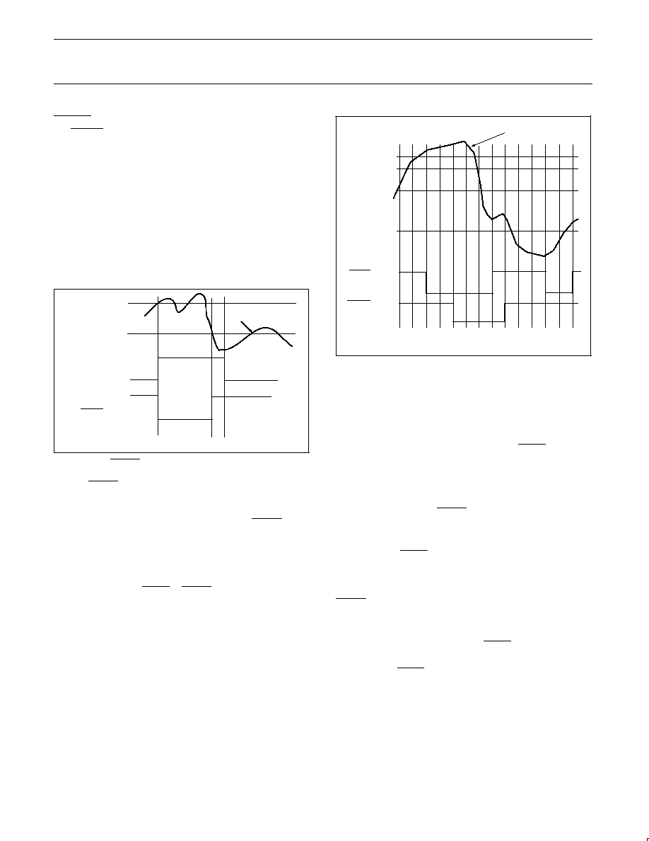
T_CRIT output
The T_CRIT output is LOW when any temperature reading is
greater than the preset limit in the corresponding critical temperature
setpoint register. When one of the T_CRIT setpoint temperatures is
exceeded, the appropriate status register bit, 1 (RCRIT) or 0
(LCRIT), is set.
After every local and remote temperature conversion the Status
register flags and the T_CRIT output are updated. Figure 7 is a
timing diagram showing the relationship of T_CRIT output, Status
bit 1 (RCRIT) and the remote critical temperature setpoint (RCS),
and critical temperature hysteresis (TH) with remote temperature
changes. Note that the T_CRIT output is de-activated only after the
remote temperature is below the remote temperature setpoint, RCS
minus the Hysteresis, TH. In the interrupt mode only, the Status
register flags are reset after the Status register is read.
RCS
RCS - TH
Status Bit 1, RCRIT
T_CRIT Output
Remote Temperature
A
B
C
SL02058
Figure 7. T_CRIT temperature response timing diagram
Event A: T_CRIT goes LOW and Status bit 1, RCRIT is set HIGH
when Remote Temperature exceeds RCS, Remote T_CRIT
Setpoint.
Event B: Remote Temperature goes below RCS-TH. T_CRIT is
deactivated, but Status Register remains unchanged.
Event C: The Status Register Bit 1, RCRIT is reset by a read of the
Status Register (in the interrupt mode).
Fault Queue
To suppress erroneous ALERT or T_CRIT triggering, the SA56004X
implements a Fault Queue for both local and remote channel. The
Fault Queue insures a temperature measurement is genuinely
beyond a HIGH, LOW or T_CRIT setpoint by not triggering until
three consecutive out-of-limit measurements have been made. The
fault queue defaults off upon POR and may be activated by setting
bit 0 in the Configuration register (address 09h) to `1'.
Remote HIGH
Setpoint
Remote LOW
Setpoint
RCS
ALERT Output
RCS -TH
Remote
Temperature
T_CRIT Output
A
B
C
D
E
F
G
H
Events
I
SL02059
NOTE: All events indicate the compeltion of a conversion.
Figure 8. Fault Queue Remote High and Low and T_CRIT,
T_CRIT Hysteresis setpoint response (Comparator mode)
At Event A: The remote temperature has exceeded the Remote
HIGH setpoint.
At Event B: Three consecutive over limit measurements have been
made exceeding the Remote HIGH setpoint; the ALERT output is
activated (goes LOW).
By now, the remote temp has exceeded the Remote T_CRIT
setpoint (RCS).
At Event C: Three consecutive over limit measurements have been
made exceeding RCS; the T_CRIT output is activated (goes LOW).
At Event D: The remote temperature falls below the RCS≠TH
setpoint.
At Event E: The ALERT output is de-activated (goes HIGH) after a
below_high_limit temperature measurement is completed.
At Event F: Three consecutive measurements have been made
with the remote temperature below the RCS≠TH threshold; the
T_CRIT output is de-activated (goes HIGH).
At Event G: The remote temp falls below the Remote LOW setpoint.
At Event H: Three consecutive measurements are made with the
temp below the Remote LOW setpoint; ALERT output is activated
(goes LOW).
At Event I: The ALERT output is de-activated (goes HIGH) after a
above_low_limit temperature measurement is completed.

Philips Semiconductors
Objective data
SA56004X
±
1
∞
C accurate, SMBus-compatible, 8-pin, remote/local
digital temperature sensor with over temperature alarms
2003 Sep 03
14
Diode fault detection
The SA56004X is designed with circuitry to detect the fault
conditions of the remote diode. When the D+ pin is shorted to V
DD
or floating, the Remote Temperature High Byte (RTHB) register is
loaded with +127
∞
C, the Remote Temperature Low Byte (RTLB)
register is loaded with 0
∞
C, and the OPEN bit (bit 2 of the Status
register) is set. Under the above conditions of D+ shorted to V
DD
or
floating, if the Remote T_CRIT setpoint is set less than +127
∞
C, and
T_CRIT Mask are disabled, then, the T_CRIT output pins will be
pulled LOW. Furthermore, if the Remote HIGH Setpoint High Byte
(RHSHB) register is set to a value less than +127
∞
C and the Alert
Mask is disabled, then the ALERT output will be pulled LOW.
Note: the OPEN bit itself will not trigger an ALERT.
When the D+ pin is shorted to ground or to D≠, the Remote
Temperature High Byte (RTHB) register is loaded with ≠128
∞
C
(1000 0000) and the OPEN (bit 2 in the Status register) will not be
set. Since operating the SA56004X is beyond its normal limits, this
temperature reading represents this shorted fault condition. If the
value in the Remote Low Setpoint High Byte (RLSHB) register is
more than ≠128
∞
C and the Alert Mask is disabled, the ALERT
output will be pulled LOW.
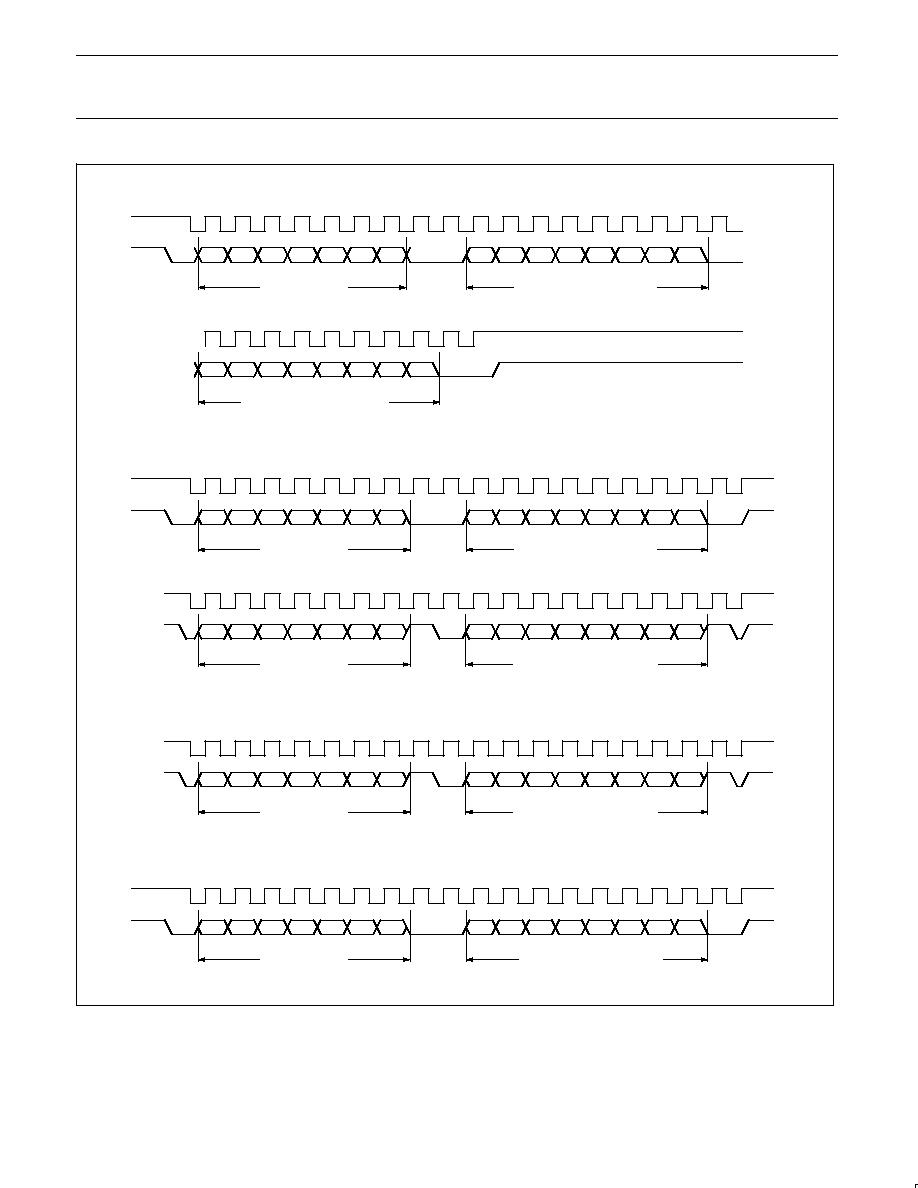
SMBus INTERFACE
The device can communicate over a standard two-wire serial
interface System Management Bus (SMBus) or compatible I
2
C-bus
using SCLK and SDATA. The device employs four standard SMBus
protocols: Write Byte, Read Byte, Receive Byte, and Send Byte.
Data formats of four protocols are shown in Figure 9. The following
key points of protocol are important:
1. The SMBus master initiates data transfer by establishing a
START condition (S) and terminates data transfer by generating
a STOP condition (P).
2. Data is sent over the serial bus in sequences of 9 clock pulses
according to each 8-bit data byte followed by 1-bit status of
device acknowledgement (A).
3. The 7-bit slave address is equivalent to factory-programmed
address of the device.
4. The command byte is equivalent to the address of the selected
device register.
5. The receive byte format is used for quicker transfer data from a
device reading register which was previously selected.
Serial interface reset
If the SMBus master attempts to reset the SA56004X while the
SA56004X is controlling the data line and transmitting on the data
line, the SA56004X must be returned to a known state in the
communication protocol. This may be accomplished in two ways:
1. When the SDATA is LOW, the SA56004X SMBus state machine
resets to the SMBus idle state if SCLK is held LOW for more
than 35 ms (maximum TIMEOUT period). According to
SMBus
specification 2.0, all devices are required to time-out when the
SCLK line is held LOW for 25 to 35 ms. Therefore, to insure a
time-out of all devices on the bus, the SCLK line must be held
LOW for at least 35 ms.
2. When the SDATA is HIGH, the master initiates an SMBus start.
The SA56004X will respond properly to a SMBus start condition
only during the data retrieving cycle. After the start, the
SA56004X will expect a SMBus Address byte.
Philips Semiconductors
Objective data
SA56004X
±
1
∞
C accurate, SMBus-compatible, 8-pin, remote/local
digital temperature sensor with over temperature alarms
2003 Sep 03
15
SL02016
WRITE BYTE FORMAT (To write a data byte to the device register) :
1
2
3
4
5
6
7
8
9
1
2
3
4
5
6
7
8
9
SCLK
(TO NEXT)
SDATA
a6
a5
a4
a3
a2
a1
(TO NEXT)
S
W
A
A
(CONT)
(CONT)
DEVICE ADDRESS
DEVICE REGISTER COMMAND
a0
D7
D6
D5
D4
D3
D2
D1
D0
1
2
3
4
5
6
7
8
9
SCLK
SDATA
D7
D6
D5
D4
D3
D2
P
A
DATA TO BE WRITTEN TO RGTR
D1
D0
READ BYTE FORMAT (To read a data byte from the device register) :
1
2
3
4
5
6
7
8
9
1
2
3
4
5
6
7
8
9
SCLK
(TO NEXT)
SDATA
a6
a5
a4
a3
a2
a1
(TO NEXT)
S
W
A
A
(CONT)
(CONT)
DEVICE ADDRESS
DEVICE REGISTER COMMAND
a0
D7
D6
D5
D4
D3
D2
D1
D0
1
2
3
4
5
6
7
8
9
SCLK
SDATA
a6
a5
a4
a3
a2
a1
A
DEVICE ADDRESS
a0
P
1
2
3
4
5
6
7
8
9
STOP
RESTART
S
R
NA
DATA FROM DEVICE REGISTER
D7
D6
D5
D4
D3
D2
D1
D0
P
STOP
RECEIVE BYTE FORMAT (To read a data byte from already pointed register) :
(CONT)
(CONT)
1
2
3
4
5
6
7
8
9
SCLK
SDATA
a6
a5
a4
a3
a2
a1
A
DEVICE ADDRESS
a0
1
2
3
4
5
6
7
8
9
RESTART
S
R
NA
DATA FROM DEVICE REGISTER
D7
D6
D5
D4
D3
D2
D1
D0
P
SEND BYTE FORMAT:
1
2
3
4
5
6
7
8
9
1
2
3
4
5
6
7
8
9
SCLK
SDATA
a6
a5
a4
a3
a2
a1
S
W
A
A
DEVICE ADDRESS
DEVICE REGISTER COMMAND
a0
D7
D6
D5
D4
D3
D2
D1
D0
P
STOP
Figure 9. SMBus interface protocols.
Philips Semiconductors
Objective data
SA56004X
±
1
∞
C accurate, SMBus-compatible, 8-pin, remote/local
digital temperature sensor with over temperature alarms
2003 Sep 03
16
Printed Circuit Board layout considerations
Care must be taken in PCB layout to minimize noise induced at the
remote temperature sensor inputs, especially in extremely noisy
environments, such as a computer motherboard. Noise induced in
the traces running between the device sensor inputs and the remote
diode can cause temperature conversion errors. Typical sensor
signal levels to the SA56004X is a few microvolts. The following
guidelines are recommended:
1. Place the SA56004X as close as possible to the remote sensor.
It can be from 4 to 8 inches, as long as the worst noise sources
such as clock generator, data and address buses, CRTs are
avoided.
2. Route the D+ and D≠ lines parallel and close together with
ground guards enclosing them (see `Ideal diode trace layout',
Figure 10).
3. Leakage currents due to PC board contamination must be
considered. Error can be introduced by these leakage currents.
4. Use wide traces to reduce inductance and noise pickup. Narrow
traces more readily pickup noise. The minimum width of 10 mil
and space of 10 mil are recommended.
5. Place a bypass capacitor of 10 nF close to the V
DD
pin and an
input filter capacitor of 2200 pF close to the D+ and D≠ pins.
6. A shielded twisted pair is recommended for a long distance
remote sensor. Connect the shield of the cable at the device
side to the SA56004X GND pin and leave the shield at the
remote end unconnected to avoid ground loop currents. Also
notice that the series resistance of the cable may introduce
measurement error; 1
can introduce about 0.5
∞
C.
GND
D+
D≠
GND
SL02017
Figure 10. Ideal diode trace layout.
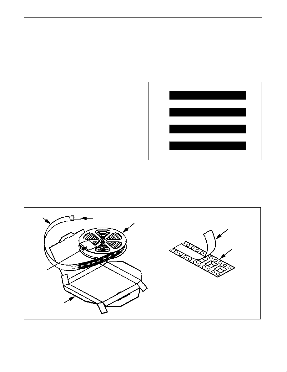
PACKING METHOD
The SA56004X is packed in reels, as shown in Figure 11.
SL01305
TAPE DETAIL
COVER TAPE
CARRIER TAPE
REEL
ASSEMBLY
TAPE
GUARD
BAND
BARCODE
LABEL
BOX
Figure 11. Tape and reel packing method
Philips Semiconductors
Objective data
SA56004X
±
1
∞
C accurate, SMBus-compatible, 8-pin, remote/local
digital temperature sensor with over temperature alarms
2003 Sep 03
17
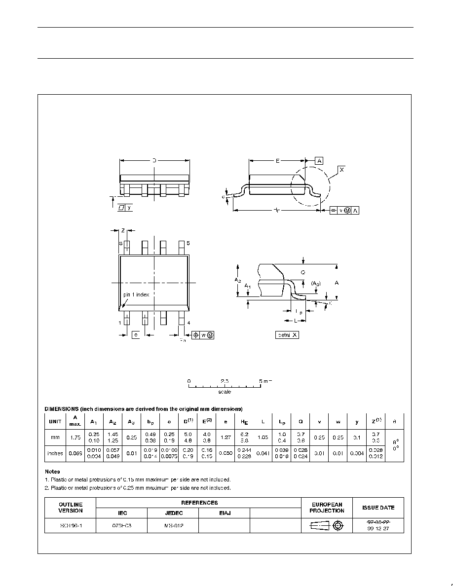
SO8:
plastic small outline package; 8 leads; body width 3.9 mm
SOT96-1
Philips Semiconductors
Objective data
SA56004X
±
1
∞
C accurate, SMBus-compatible, 8-pin, remote/local
digital temperature sensor with over temperature alarms
2003 Sep 03
18
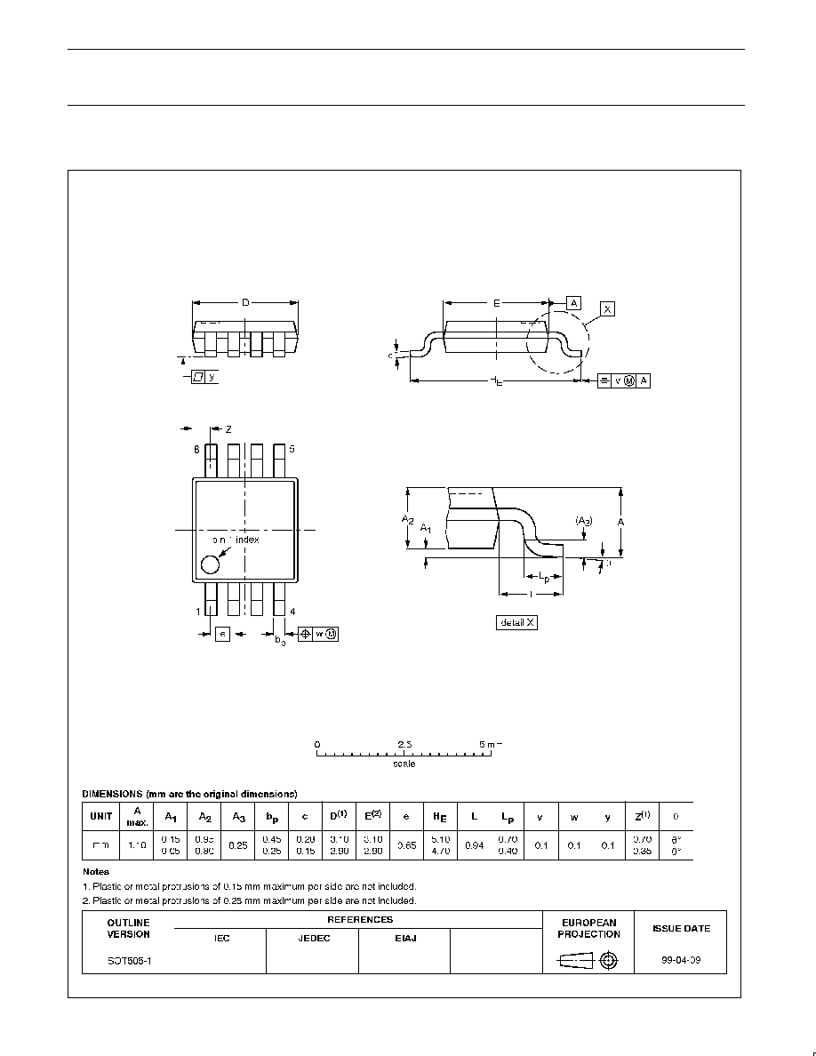
TSSOP8:
plastic thin shrink small outline package; 8 leads; body width 3 mm
SOT505-1
Philips Semiconductors
Objective data
SA56004X
±
1
∞
C accurate, SMBus-compatible, 8-pin, remote/local
digital temperature sensor with over temperature alarms
2003 Sep 03
19
REVISION HISTORY
Rev
Date
Description
_2
20030903
Objective data (9397 750 12015). Replaces SA56004-X_1 dated 2003 Aug 19 (9397 750 10993).
Modifications:
∑
Part number shown on document changed from SA56004-X to SA56004X (ordering codes remain as-is).
∑
Added I
2
C-bus logos.
_1
20030819
Objective data (9397 750 10993).
Philips Semiconductors
Objective data
SA56004X
±
1
∞
C accurate, SMBus-compatible, 8-pin, remote/local
digital temperature sensor with over temperature alarms
2003 Sep 03
20
Purchase of Philips I
2
C components conveys a license under the Philips' I
2
C patent
to use the components in the I
2
C system provided the system conforms to the
I
2
C specifications defined by Philips. This specification can be ordered using the
code 9398 393 40011.
Definitions
Short-form specification -- The data in a short-form specification is extracted from a full data sheet with the same type number and title. For detailed information see
the relevant data sheet or data handbook.
Limiting values definition -- Limiting values given are in accordance with the Absolute Maximum Rating System (IEC 60134). Stress above one or more of the limiting
values may cause permanent damage to the device. These are stress ratings only and operation of the device at these or at any other conditions above those given
in the Characteristics sections of the specification is not implied. Exposure to limiting values for extended periods may affect device reliability.
Application information -- Applications that are described herein for any of these products are for illustrative purposes only. Philips Semiconductors make no
representation or warranty that such applications will be suitable for the specified use without further testing or modification.
Disclaimers
Life support -- These products are not designed for use in life support appliances, devices, or systems where malfunction of these products can reasonably be
expected to result in personal injury. Philips Semiconductors customers using or selling these products for use in such applications do so at their own risk and agree
to fully indemnify Philips Semiconductors for any damages resulting from such application.
Right to make changes -- Philips Semiconductors reserves the right to make changes in the products--including circuits, standard cells, and/or software--described
or contained herein in order to improve design and/or performance. When the product is in full production (status `Production'), relevant changes will be communicated
via a Customer Product/Process Change Notification (CPCN). Philips Semiconductors assumes no responsibility or liability for the use of any of these products, conveys
no license or title under any patent, copyright, or mask work right to these products, and makes no representations or warranties that these products are free from patent,
copyright, or mask work right infringement, unless otherwise specified.
Contact information
For additional information please visit
http://www.semiconductors.philips.com.
Fax: +31 40 27 24825
For sales offices addresses send e-mail to:
sales.addresses@www.semiconductors.philips.com.
©
Koninklijke Philips Electronics N.V. 2003
All rights reserved. Printed in U.S.A.
Date of release: 09-03
Document order number:
9397 750 12015
Philips
Semiconductors
Data sheet status
[1]
Objective data
Preliminary data
Product data
Product
status
[2] [3]
Development
Qualification
Production
Definitions
This data sheet contains data from the objective specification for product development.
Philips Semiconductors reserves the right to change the specification in any manner without notice.
This data sheet contains data from the preliminary specification. Supplementary data will be published
at a later date. Philips Semiconductors reserves the right to change the specification without notice, in
order to improve the design and supply the best possible product.
This data sheet contains data from the product specification. Philips Semiconductors reserves the
right to make changes at any time in order to improve the design, manufacturing and supply. Relevant
changes will be communicated via a Customer Product/Process Change Notification (CPCN).
Data sheet status
[1] Please consult the most recently issued data sheet before initiating or completing a design.
[2] The product status of the device(s) described in this data sheet may have changed since this data sheet was published. The latest information is available on the Internet at URL
http://www.semiconductors.philips.com.
[3] For data sheets describing multiple type numbers, the highest-level product status determines the data sheet status.
Level
I
II
III