Document Outline
- GENERAL DESCRIPTION
- FEATURES
- APPLICATIONS
- SIMPLIFIED SYSTEM DIAGRAM
- ORDERING INFORMATION
- PIN CONFIGURATION
- PIN DESCRIPTION
- MAXIMUM RATINGS
- ELECTRICAL CHARACTERISTICS
- APPLICATION INFORMATION
- PACKING METHOD
- PACKAGE OUTLINE
- REVISION HISTORY
- Data sheet status
- Definitions
- Disclaimers
Philips
Semiconductors
SA57022-XX
500 mA LDO with ON/OFF control and
V
ref
bypass
Product data
Supersedes data of 2001 Oct 03
2003 Oct 13
INTEGRATED CIRCUITS
Philips Semiconductors
Product data
SA57022-XX
500 mA LDO with ON/OFF control and V
ref
bypass
2
2003 Oct 13
GENERAL DESCRIPTION
The SA57022-XX has an extremely precise fixed output with a
typical accuracy of
±
2%. It is designed to provide very low dropout
and ultra low noise with an optional Bypass pin, and fast transient
response. Supply current is reduced to zero (typical).
The SA57022-XX incorporates both over-temperature and
over-current protection. The SA57022-XX is stable with an output
capacitor of only 1.0
µ
F and has a maximum output current of
500 mA. It is available in the 7-pin small outline package (SOP002).
FEATURES
∑
Very low dropout voltage: 300 mV typ. (I
out
= 500 mA)
∑
High precision output voltage:
±
2%
∑
Output current capacity: 500 mA
∑
Low noise: 75
µ
V
rms
typ. @ 20 Hz to 80 KHz, for C
n
= 470 pF.
∑
Extremely good line regulation: 10 mV typical
∑
Extremely good load regulation: 20 mV typical
∑
Low temperature drift co-efficient to V
out
:
±
100 ppm/
∞
C
∑
Internal current limit and thermal shut-down circuits
∑
Input voltage range: ≠0.3 V to 12 V
∑
Wide preset output voltage range: 1.8 V to 5 V
∑
Wide operating temperature range: ≠40
∞
C to +85
∞
C
APPLICATIONS
∑
Battery-operated systems
∑
Portable computers
∑
Cameras, VCRs and camcorders
∑
PCMCIA cards, modems, pagers
∑
Cellular/GSM/PHS phones
∑
Linear post-regulator for SMPS
∑
Instrumentation
SIMPLIFIED SYSTEM DIAGRAM
V
IN
BYPASS
V
OUT
GND
7
1
4
3
5
ON/OFF
R
R
CURRENT
LIMIT
REFERENCE
BIAS
DRIVER
THERMAL
SHUTDOWN
SL01527
Figure 1. Simplified system diagram.
Philips Semiconductors
Product data
SA57022-XX
500 mA LDO with ON/OFF control and V
ref
bypass
2003 Oct 13
3
ORDERING INFORMATION
TYPE NUMBER
PACKAGE
TEMPERATURE
TYPE NUMBER
DESCRIPTION
VERSION
RANGE
SA57022-XXD
small outline 7-pin surface mount (see dimensional drawing)
SOP002
≠40 to +85
∞
C
NOTE:
The device has six voltage output options, indicated by the XX on
the order code.
XX
VOLTAGE (Typical)
18
1.8 V
25
2.5 V
28
2.8 V
30
3.0 V
33
3.3 V
50
5.0 V
Part number marking
Each package is marked with a four letter code. The first three
letters designate the product. The fourth letter, represented by `x', is
a date tracking code.
Part number
Marking
SA57022-18
A L M x
SA57022-25
A L N x
SA57022-28
A L P x
SA57022-30
A L R x
SA57022-33
A L S x
SA57022-50
A L T x
PIN CONFIGURATION
SL01525
1
2
4
5
7
V
IN
ON/OFF
BYPASS
NC
V
OUT
SA57022-XX
3
GND
6
GND
Figure 2. Pin configuration.
PIN DESCRIPTION
PIN
SYMBOL
DESCRIPTION
1
V
OUT
Regulated output voltage.
2
NC
No connection.
3
GND
Ground.
4
BYPASS
Reference bypass input. Connecting a
470 pF capacitor further reduces output
noise.
5
ON/OFF
Output voltage On/Off control pin.
6
GND
Substrate ground pin. This pin must be
connected to ground.
7
V
IN
Power supply input.
MAXIMUM RATINGS
SYMBOL
PARAMETER
MIN.
MAX.
UNIT
V
IN
Supply voltage
≠0.3
+12
V
V
IN(OPR)
Operating voltage
V
OUT(typ)
+ 0.5
V
OUT(typ)
+ 10
V
I
OUT
Output current
0
500
mA
T
oper
Operating temperature
≠40
+85
∞
C
T
stg
Storage temperature
≠40
+150
∞
C
P
D
Power dissipation (Note 1)
≠
400
mW
P
D
Power dissipation (Note 2)
≠
950
mW
NOTES:
1. Unattached.
2. Mounted on double-sided glass epoxy PCB, with copper ground plane 192
◊
142
◊
1.2 mm.
Philips Semiconductors
Product data
SA57022-XX
500 mA LDO with ON/OFF control and V
ref
bypass
2003 Oct 13
4
ELECTRICAL CHARACTERISTICS
T
amb
= 25
∞
C; V
ON/OFF
= 1.6 V, unless otherwise specified.
SYMBOL
PARAMETER
CONDITIONS
MIN.
TYP.
MAX.
UNIT
I
CC
No-load input current
I
OUT
= 0 mA
≠
1.9
5
mA
I
CC(OFF)
Input current (off)
V
ON/OFF
= 0 V
≠
0
1
µ
A
V
OUT
Output voltage (as % of V
nom
)
I
OUT
= 250 mA
98%
≠
102%
V
SA57022-18
1.764
1.8
1.836
V
SA57022-25
2.450
2.5
2.550
V
SA57022-28
2.744
2.8
2.856
V
SA57022-30
2.940
3.0
3.060
V
SA57022-33
3.234
3.3
3.060
V
SA57022-50
4.900
5.0
5.100
V
V
IO
Dropout voltage (Note 2)
V
IN
= V
OUT
≠ 0.2 V; I
OUT
= 250 mA
≠
0.3
0.5
V
V1
Line regulation
V
IN
= V
OUT
+1.5 V to V
IN
= V
OUT
+2.5 V;
I
OUT
= 250 mA
≠
10
20
mV
V2
Load regulation
I
OUT
= 0 to 250 mA
≠
20
120
mV
V
OUT
/
T
V
OUT
Temperature coefficient
(Note 1)
T
j
= ≠30 to +85
∞
C
≠
100
≠
ppm/
∞
C
RR
Ripple rejection (Note 1)
f = 120 Hz; V
ripple
= 1 V; I
OUT
= 250 mA
50
64
≠
dB
V
n
Output noise voltage (Note 1)
f
BW
= 20 to 80 kHz; C
n
= 470 pF
≠
75
≠
µ
V
rms
I
ON/OFF
ON/OFF pin input current
V
ON/OFF
= V
IN
10
20
30
µ
A
V
ON/OFF(H)
ON/OFF HIGH threshold voltage
1.6
≠
V
IN
+0.3
V
V
ON/OFF(L)
ON/OFF LOW threshold voltage
-0.3
≠
0.4
V
NOTES:
1. The parameter is guaranteed by design.
2. This parameter is not guaranteed if V
OUT
is less than 2 V.
Philips Semiconductors
Product data
SA57022-XX
500 mA LDO with ON/OFF control and V
ref
bypass
2003 Oct 13
5
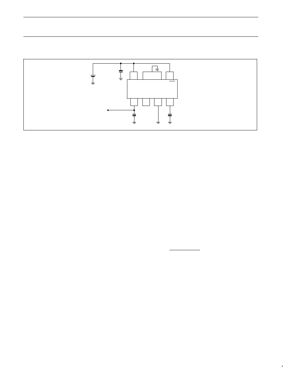
APPLICATION INFORMATION
2
3
1
5
4
6
7
V
OUT
NC
GND
BYPASS
V
IN
SUB
ON/OFF
C
IN
= 1
µ
F
CERAMIC
C
n
= 470 pF
CERAMIC
VOLTAGE
INPUT
TO LOAD
C
OUT
= 2.2
µ
F
CERAMIC
SL01526
Figure 3. Typical application circuit.
Input capacitor
An input capacitor of 1.0
µ
F (min) should be connected from V
IN
to
GND if there is more than 10 inches of wire between the regulator
and the AC filter capacitor, or if a battery is operated as the power
source. The capacitor should be less than 1 cm from the input pin.
Aluminum electrolytic or tantalum capacitor types can be used.
(Because many aluminum electrolytic capacitors freeze at
approximately ≠30
∞
C, solid tantalums are recommended for
applications operating below ≠25
∞
C.) When operating from sources
other than batteries, supply-noise rejection and transient response
can be improved by increasing the value of the input and output
capacitors and employing passive filtering techniques.
Output capacitor
Phase compensation is used to ensure stable operation even if load
current varies. For this reason, an output capacitor with good
frequency characteristics is needed. Set it as close to the circuit as
possible, with wires as short as possible. A 1.0
µ
F capacitor from
V
OUT
to ground is recommended. The output capacitor should have
an ESR (effective series resistance) of 5.0
or less, and a resonant
frequency above 1.0 MHz.
Optional BYPASS capacitor
A 470 pF capacitor connected from the BYPASS input to ground
reduces noise present on the internal reference, which in turn
significantly reduces output noise. This capacitor must have low
leakage, because the pin is high impedance. If output noise is not a
concern, this pin may be left unconnected. Larger capacitor values
may be used, but results in a longer time period to rated output
voltage when power is initially applied.
ON/OFF
The regulator is fully enabled when a logic HIGH is applied to this
input. The regulator enters shutdown when a logic LOW is appplied
to this input. During shutdown, regulator output voltage falls to
zero,and supply current is reduced to 1.0
µ
A max, and V
OUT
falls to
zero. For use as an always-on regulator, connect ON/OFF pin to the
supply voltage, as shown in Figure 3.
Optional BYPASS diode
If the voltage on the output pin rises above the input voltage, as
might happen in some applications, the overcurrrent will flow via
internal parasitic diodes from output to input. To prevent this,
connect a bypass diode between the output and input pins.
Thermal shutdown
Integrated thermal protection circuitry shuts the regulator off when
die temperature exceeds 150
∞
C. The regulator remains off until the
die temperature drops to approximately 140
∞
C.
Power dissipation
The amount of power the regulator dissipates is primarily a function
of input and output voltage, and output current. The following
equation is used to calculate worst case actual power dissipation:
P
D
[
V
IN(max)
*
V
OUT(min)
I
LOAD(max)
Eqn. (1)
Where:
P
D
= worst case actual power dissipation
V
IN(max)
= maximum voltage on V
IN
V
OUT(min)
= minimum regulator output voltage
I
LOAD(max)
= maximum output (load) current
The maximum allowable power dissipation, as shown in Equation (2),
is a function of the maximum ambient temperature (T
amb(max)
), the
maximum allowable die temperature (125
∞
C), and the thermal
resistance from junction-to-air (R
th(j≠a)
).
Eqn. (2)
P
D(max)
+
T
j(max)
*
T
amb(max)
R
th(j
*
a)
The SUB (heat sink) pin must be connected to ground with a wide
trace.
PCB layout hints
The component placement around the LDO should be done carefully
to achieve good dynamic line and load response. The input and
noise capacitor should be kept close to the LDO. The rise in junction
temperature depends on how efficiently the heat is carried away
from the junction to ambient. The junction to lead thermal
impedance is a characteristic of the package and fixed. The thermal
impedance between lead to ambient can be reduced by increasing
the copper area on PCB. Increase the input, output and ground
trace area to reduce the junction-to-ambient impedance.
Philips Semiconductors
Product data
SA57022-XX
500 mA LDO with ON/OFF control and V
ref
bypass
2003 Oct 13
6
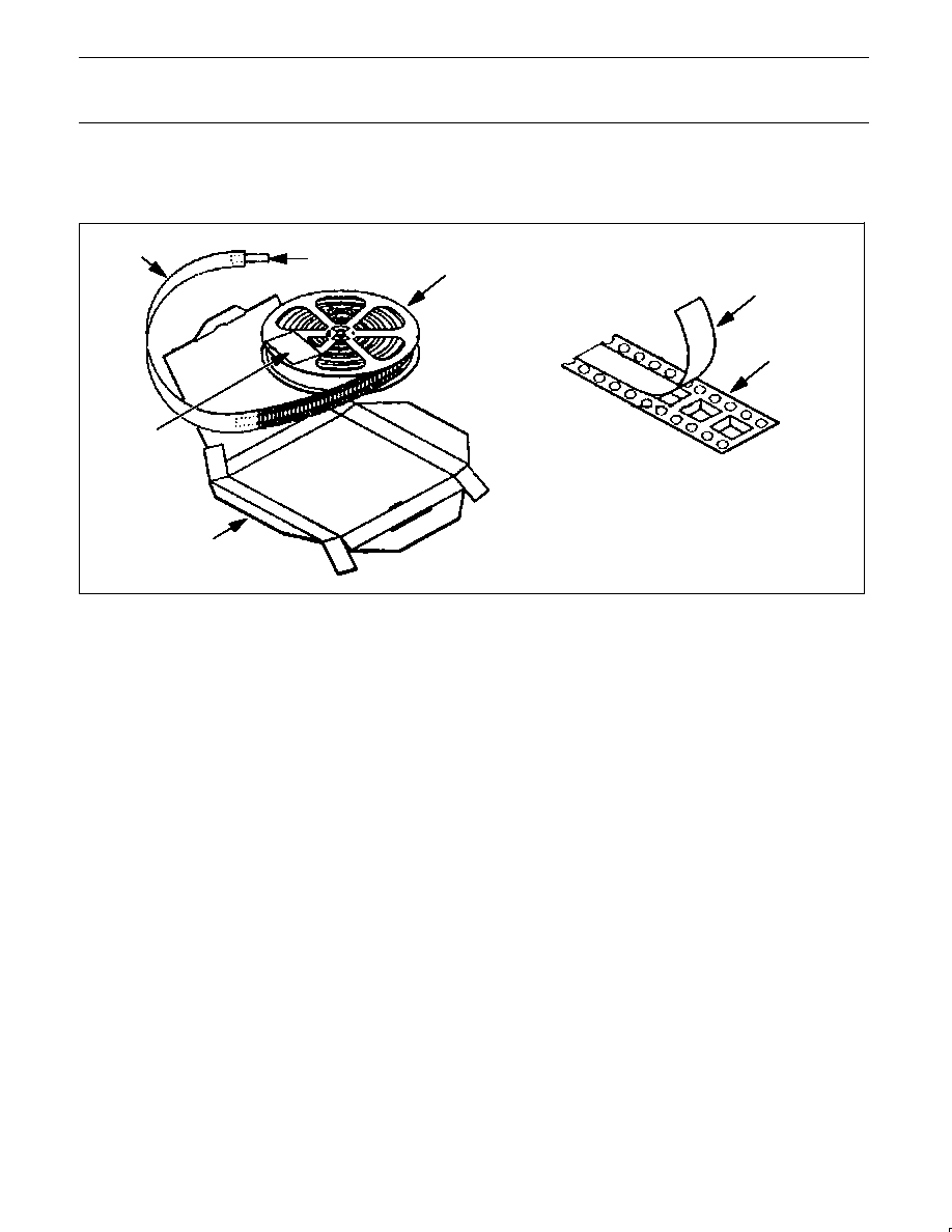
PACKING METHOD
The SA57003 is packed in reels, as shown in Figure 4.
SL01305
TAPE DETAIL
COVER TAPE
CARRIER TAPE
REEL
ASSEMBLY
TAPE
GUARD
BAND
BARCODE
LABEL
BOX
Figure 4. Tape and reel packing method
Philips Semiconductors
Product data
SA57022-XX
500 mA LDO with ON/OFF control and V
ref
bypass
2003 Oct 13
7
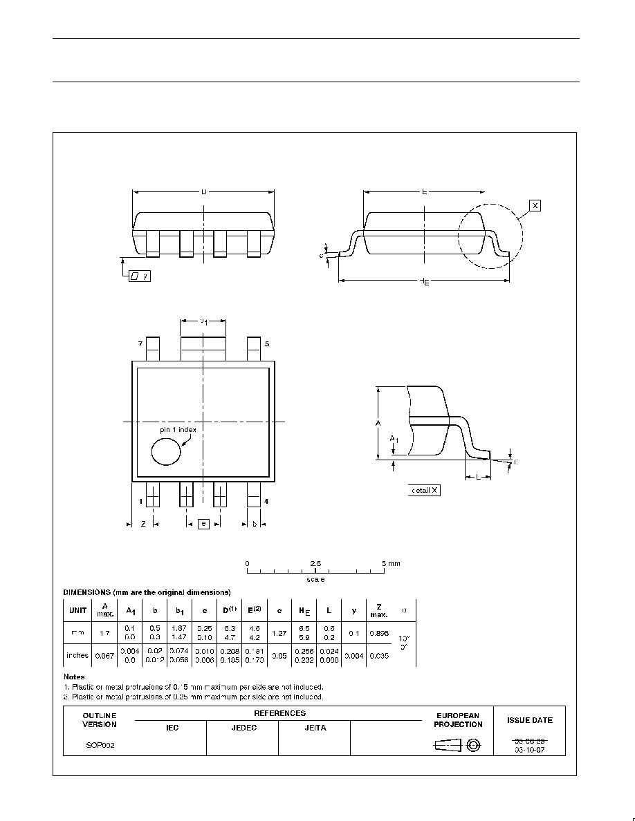
Plastic small outline package; 7 leads; body width 4.4 mm
SOP002
Philips Semiconductors
Product data
SA57022-XX
500 mA LDO with ON/OFF control and V
ref
bypass
2003 Oct 13
8
REVISION HISTORY
Rev
Date
Description
_2
20031013
Product data (9397 750 12112). ECN 853-2293 30328 of 09 September 2003.
Modifications:
∑
Change package name from SOP-7B to SOP002 in Ordering information and Package outline sections.
_1
20011003
Product data (9397 750 08967). ECN 853-2293 27197 of 03 October 2001.
Definitions
Short-form specification -- The data in a short-form specification is extracted from a full data sheet with the same type number and title. For detailed information see
the relevant data sheet or data handbook.
Limiting values definition -- Limiting values given are in accordance with the Absolute Maximum Rating System (IEC 60134). Stress above one or more of the limiting
values may cause permanent damage to the device. These are stress ratings only and operation of the device at these or at any other conditions above those given
in the Characteristics sections of the specification is not implied. Exposure to limiting values for extended periods may affect device reliability.
Application information -- Applications that are described herein for any of these products are for illustrative purposes only. Philips Semiconductors make no
representation or warranty that such applications will be suitable for the specified use without further testing or modification.
Disclaimers
Life support -- These products are not designed for use in life support appliances, devices, or systems where malfunction of these products can reasonably be
expected to result in personal injury. Philips Semiconductors customers using or selling these products for use in such applications do so at their own risk and agree
to fully indemnify Philips Semiconductors for any damages resulting from such application.
Right to make changes -- Philips Semiconductors reserves the right to make changes in the products--including circuits, standard cells, and/or software--described
or contained herein in order to improve design and/or performance. When the product is in full production (status `Production'), relevant changes will be communicated
via a Customer Product/Process Change Notification (CPCN). Philips Semiconductors assumes no responsibility or liability for the use of any of these products, conveys
no license or title under any patent, copyright, or mask work right to these products, and makes no representations or warranties that these products are free from patent,
copyright, or mask work right infringement, unless otherwise specified.
Contact information
For additional information please visit
http://www.semiconductors.philips.com.
Fax: +31 40 27 24825
For sales offices addresses send e-mail to:
sales.addresses@www.semiconductors.philips.com.
©
Koninklijke Philips Electronics N.V. 2003
All rights reserved. Printed in U.S.A.
Date of release: 10-03
Document order number:
9397 750 12112
Philips
Semiconductors
Data sheet status
[1]
Objective data
Preliminary data
Product data
Product
status
[2] [3]
Development
Qualification
Production
Definitions
This data sheet contains data from the objective specification for product development.
Philips Semiconductors reserves the right to change the specification in any manner without notice.
This data sheet contains data from the preliminary specification. Supplementary data will be published
at a later date. Philips Semiconductors reserves the right to change the specification without notice, in
order to improve the design and supply the best possible product.
This data sheet contains data from the product specification. Philips Semiconductors reserves the
right to make changes at any time in order to improve the design, manufacturing and supply. Relevant
changes will be communicated via a Customer Product/Process Change Notification (CPCN).
Data sheet status
[1] Please consult the most recently issued data sheet before initiating or completing a design.
[2] The product status of the device(s) described in this data sheet may have changed since this data sheet was published. The latest information is available on the Internet at URL
http://www.semiconductors.philips.com.
[3] For data sheets describing multiple type numbers, the highest-level product status determines the data sheet status.
Level
I
II
III