 | –≠–ª–µ–∫—Ç—Ä–æ–Ω–Ω—ã–π –∫–æ–º–ø–æ–Ω–µ–Ω—Ç: SA57031 | –°–∫–∞—á–∞—Ç—å:  PDF PDF  ZIP ZIP |
Document Outline
- GENERAL DESCRIPTION
- FEATURES
- APPLICATIONS
- SIMPLIFIED DEVICE DIAGRAM
- ORDERING INFORMATION
- PIN CONFIGURATION
- PIN DESCRIPTION
- MAXIMUM RATINGS
- ELECTRICAL CHARACTERISTICS
- TYPICAL PERFORMANCE CURVES
- TECHNICAL DISCUSSION
- APPLICATION INFORMATION
- TEST CIRCUIT
- PACKING METHOD
- Data sheet status
- Definitions
- Disclaimers

Philips
Semiconductors
SA57005
Multiple output low noise, low dropout
linear regulator
Product data
2002 Jun 20
INTEGRATED CIRCUITS
Philips Semiconductors
Product data
SA57005
Multiple output low noise, low dropout linear regulator
2
2002 Jun 20
853-2352 28505
GENERAL DESCRIPTION
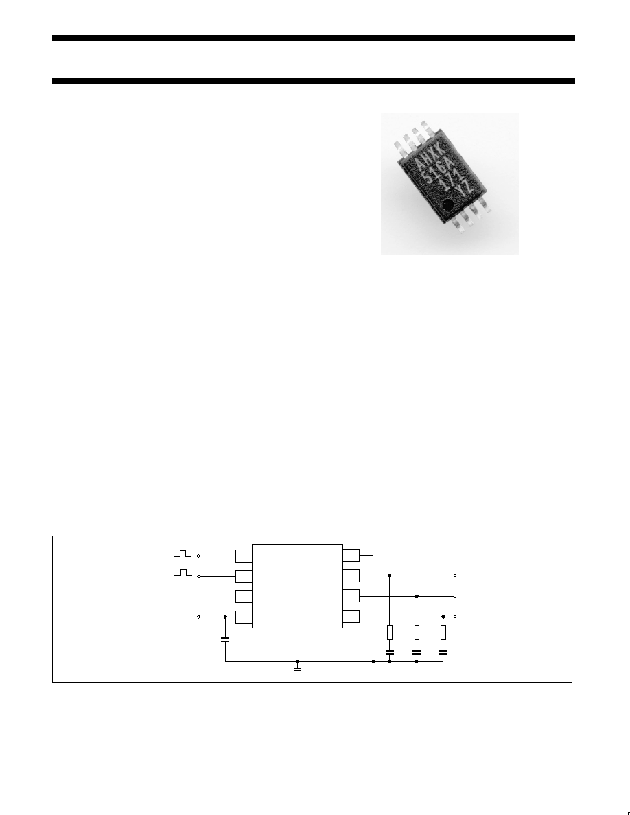
The SA57005 is a very low dropout, low noise composite voltage
regulator with three fixed independent outputs. The output voltages
are preset to 2.5 V, 2.8 V and 3.0 V having a common input voltage
pin V
IN
. Two ON/OFF switches allow V
o1
and V
o2
/V
o3
to be turned
off when not needed, thus conserving power. Also, three regulators
in one package save board space, which is critical in
microprocessor systems.
Designed for battery-powered and portable applications the
SA57005 achieves unequalled performance in all specifications
such as low supply-current, low dropout voltage, low power
consumption, small size, fast dynamic response to line and load,
precision output and so on. Each of these regulators consists of an
internal voltage reference, an error amplifier, resistors, and control
switch. The SA57005 is housed in a VSOP-8A 8-lead package.
FEATURES
∑
Very low dropout voltage:
V
o1
:
0.25 V typ.; V
o2
:
0.28 V typ.;
V
o3
:
0.30 V typ.
∑
Low noise:
60
µ
V
rms
typ. (f = 10 Hz to 10 kHz; I
O
= 30 mA)
∑
High precision output voltage:
±
3%
∑
Output current capacity:
I
o1
and I
o2
= 100 mA max; I
o3
= 150 mA max.
∑
Low consumption current:
I
IN1
= 250
µ
A typ.,
I
IN2
/I
IN3
= 500
µ
A typ. (when not loaded), 3
µ
A max. (when off)
∑
Line regulation:
1%/V typ. (I
OUT
= 30 mA; V
IN
= 4.0 to 8.0 V)
∑
Load regulation:
30 mV typ. for I
OUT
= 0 to 70 mA
∑
Low temperature drift co-efficient to V
OUT
:
±
100 ppm/
∞
C
∑
Thermal shutdown
∑
Wide operating temperature range:
≠20
∞
C to +75
∞
C
APPLICATIONS
∑
Cellular phones, cordless phones and 2-way radios
∑
Electronic notebooks, PDAs and Palmtop computers
∑
Cameras, VCRs and camcorders
∑
Modems
∑
Battery-powered or hand-held instruments
SIMPLIFIED DEVICE DIAGRAM
2
3
1
5
4
6
7
8
1
µ
F
PS1
PS2/3
NC
V
IN
1
1
1
1
µ
F
1
µ
F
1
µ
F
GND
V
o1
V
o2
V
o3
SL01698
SA57005
Figure 1. Simplified device diagram.

Philips Semiconductors
Product data
SA57005
Multiple output low noise, low dropout linear regulator
2002 Jun 20
3
ORDERING INFORMATION
TYPE NUMBER
PACKAGE
TYPE NUMBER
NAME
DESCRIPTION
TEMPERATURE RANGE
SA57005DH
VSOP-8A
8-pin surface mount small outline package
≠20 to +75
∞
C
Part number marking
Each device is marked with a four letter code on the first line. The
first three letters designate the product. The fourth letter,
represented by `x' is a date tracking code. Any other lines contain
manufacturing codes.
Part Number
Marking
SA57005DH
AHXx
PIN CONFIGURATION
SL01697
1
2
3
4
5
6
7
8
PS1
PS2/3
NC
V
IN
GND
V
o1
V
o2
V
o3
TOP VIEW
SA57005
Figure 2. Pin configuration.
PIN DESCRIPTION
PIN
SYMBOL
DESCRIPTION
1
PS1
ON/OFF control for V
o1
;
tie to V
IN
if ON/OFF function is not used.
2
PS2/3
ON/OFF control for V
o2
and V
o3
;
tie to V
IN
if ON/OFF function is not used.
3
NC
No connection
4
V
IN
Input voltage
5
V
o3
Regulated output 3
6
V
o2
Regulated output 2
7
V
o1
Regulated output 1
8
GND
Ground
MAXIMUM RATINGS
SYMBOL
PARAMETER
CONDITIONS
Min.
Max.
UNIT
V
IN
Supply voltage
≠0.3
+12
V
I
O1
, I
O2
Output current 1, 2
≠
100
mA
I
O3
Output current 3
≠
150
mA
T
opr
Operating ambient temperature range
≠20
+75
∞
C
T
stg
Storage temperature
≠40
+125
∞
C
P
D
Power dissipation
unmounted
≠
300
mW
when mounted on glass epoxy board
(40
◊
40
◊
1.6 mm)
≠
500
mW

Philips Semiconductors
Product data
SA57005
Multiple output low noise, low dropout linear regulator
2002 Jun 20
4
ELECTRICAL CHARACTERISTICS
T
amb
= 25
∞
C; V
IN
= 4 V; C
IN
= 2.2
µ
F; C
VO(n)
= 2.2
µ
F; unless otherwise specified.
SYMBOL
PARAMETER
CONDITIONS
Min.
Typ.
Max.
UNIT
I
IN(OFF)
Supply current (OFF)
V
PS1
= V
PS2/3
= 0 V
≠
0
3
µ
A
I
IN1
, I
IN2
, I
IN3
Supply current 1, 2, 3
no load
I
IN1
V
PS1
= 3 V; V
PS2/3
= 0 V
≠
250
370
µ
A
I
IN2
, I
IN3
V
PS2/3
= 3 V; V
PS1
= 0 V
≠
500
740
µ
A
V
o1
V
o1
Output voltage
I
O1
= 30 mA
2.42
2.50
2.58
V
V
io(dif)(min)1
Input/output differential voltage
V
IN
= 2.3 V; I
O1
= 30 mA
≠
0.1
0.25
V
V
LO1
Load regulation
I
O1
= 0 to 70 mA
≠
30
60
mV
V
LI1
Line regulation
V
IN
= 4.0 V to 8.0 V; I
O1
= 30 mA
≠
10
25
mV
V
o1
/
T
V
O
temperature coefficient
(Note 1)
T
amb
= ≠20
∞
C to +75
∞
C; I
O1
= 30 mA
≠
±
100
≠
ppm/
∞
C
RR1
Ripple rejection (Note 1)
f = 120 Hz; V
ripple
= 1 V
p-p
; I
O1
= 30 mA
50
60
≠
dB
V
n1
Output noise voltage (Note 1)
f = 10 Hz to 10 kHz; I
O1
= 30 mA
≠
60
90
µ
V
rms
t
DH1
Output delay time (Note 1)
I
O1
= 30 mA; V
PS1
= 0 V
4 V;
V
PS2/3
= 0 V
≠
0.04
0.15
ms
V
o2
V
o2
Output voltage
I
O2
= 30 mA
2.72
2.80
2.88
V
V
io(dif)(min)2
Input/output differential voltage
V
IN
= 2.6 V; I
O2
= 30 mA
≠
0.1
0.25
V
V
LO2
Load regulation
I
O2
= 0 to 70 mA
≠
30
60
mV
V
LI2
Line regulation
V
IN
= 4.0 V to 8.0 V; I
O2
= 30 mA
≠
10
25
mV
V
o2
/
T
V
O
temperature coefficient
(Note 1)
T
amb
= ≠20
∞
C to +75
∞
C; I
O2
= 30 mA
≠
±
100
≠
ppm/
∞
C
RR2
Ripple rejection (Note 1)
f = 120 Hz; V
ripple
= 1 V
p-p
; I
O2
= 30 mA
50
60
≠
dB
V
n2
Output noise voltage (Note 1)
f = 10 Hz to 10 kHz; I
O2
= 30 mA
≠
60
90
µ
V
rms
t
DH2
Output delay time (Note 1)
I
O2
= 30 mA; V
PS2/3
= 0 V
4 V;
V
PS1
= 0 V
≠
0.04
0.15
ms
V
o3
V
o3
Output voltage
I
O3
= 80 mA
2.92
3.00
3.08
V
V
io(dif)(min)3
Input/output differential voltage
V
IN
= 2.8 V; I
O3
= 80 mA
≠
0.15
0.30
V
V
LO3
Load regulation
I
O3
= 0 to 100 mA
≠
30
60
mV
V
LI3
Line regulation
V
IN
= 4.0 V to 8.0 V; I
O3
= 30 mA
≠
10
25
mV
V
o3
/
T
V
O
temperature coefficient
(Note 1)
T
amb
= ≠20
∞
C to +75
∞
C; I
O3
= 30 mA
≠
±
100
≠
ppm/
∞
C
RR3
Ripple rejection (Note 1)
f = 120 Hz; V
ripple
= 1 V
p-p
; I
O3
= 30 mA
50
60
≠
dB
V
n3
Output noise voltage (Note 1)
f = 10 Hz to 10 kHz; I
O3
= 30 mA
≠
60
90
µ
V
rms
t
DH3
Output delay time (Note 1)
I
O3
= 30 mA; V
PS2/3
= 0 V
4 V
≠
0.04
0.15
ms
PS output control pin
V
OFF
LOW-level threshold voltage
≠
≠
0.4
V
V
ON
HIGH-level threshold voltage
1.6
≠
≠
V
I
PS1
PS1 terminal current
V
PS1
= 1.6 V
≠
≠
8
µ
A
I
PS2/3
PS2/3 terminal current
V
PS2/3
= 1.6 V
≠
≠
16
µ
A
NOTE:
1. Guaranteed by design.

Philips Semiconductors
Product data
SA57005
Multiple output low noise, low dropout linear regulator
2002 Jun 20
5
TYPICAL PERFORMANCE CURVES
INPUT≠OUTPUT
(mV)
SL01699
OUTPUT CURRENT (mA)
0.0
50.0
100.0
150.0
200.0
250.0
0
50
100
150
Figure 3. Input-output differential voltage.
LINE REGULA
TION
(mV)
SL01700
V
IN
(V)
≠20.0
≠10.0
0.0
10.0
20.0
4
6
8
10
12
Figure 4. Line regulation.
LOAD REGULA
TION
(mV)
SL01703
OUTPUT CURRENT (mA)
≠40.0
≠30.0
≠20.0
≠10.0
0.0
10.0
20.0
30.0
40.0
0
50
100
150
Figure 5. Load regulation.
OUTPUT VOL
T
AGE (V)
SL01702
TEMPERATURE (
∞
C)
0.0
1.0
2.0
3.0
4.0
0
50
100
150
200
Figure 6. Thermal shutdown.
OUTPUT VOL
T
AGE (V)
SL01701
OUTPUT CURRENT (mA)
0.0
1.0
2.0
3.0
4.0
0
100
200
300
Figure 7. Current limit.
EQUIV
ALENT
SERIES
RESIST
ANCE ( )
SL01708
LOAD CURRENT (mA)
100
10
1
0.1
0.01
0
50
100
150
STABLE
UNSTABLE
UNSTABLE
Figure 8. ESR stability.

Philips Semiconductors
Product data
SA57005
Multiple output low noise, low dropout linear regulator
2002 Jun 20
6
SL01704
TEMPERATURE (
∞
C)
0
100
200
300
400
500
600
700
800
0
50
100
150
POWER DISSIP
A
TION
(mW)
ON BOARD
(40
◊
40
◊
1.6 mm)
ALONE
Figure 9. Power dissipation.

Philips Semiconductors
Product data
SA57005
Multiple output low noise, low dropout linear regulator
2002 Jun 20
7
TECHNICAL DISCUSSION
As illustrated in the circuit diagram, each of the regulators in the
SA57005 consists of a voltage reference, an error amplifier,
P-channel pass transistor, current limit circuit and an internal
feedback voltage divider. The output voltage is fed back through an
internal resistor voltage divider connected to the output voltage pins.
The reference will be activated if any of the PS1 and PS2/3 switches
is turned on.
The reference is connected to the error amplifier's non-inverting
input. The error amplifier compares the reference with the feedback
voltage and amplifies the difference. If the feedback voltage is lower
than the reference voltage the output of the error amplifier goes up,
which pulls down the pass transistor's gate. This allows more
current to pass to the output and increase the output voltage. On the
other hand, if the feedback voltage is too high the pass transistor
gate is pulled up, allowing less current to pass to the output,
resulting a decrease in output voltage.
SL01705
5 V
o3
8 GND
6 V
o2
7 V
o1
2
PS2/3
1
PS1
TERMINAL
PROTECT
4
V
IN
Figure 10. Functional diagram.

Philips Semiconductors
Product data
SA57005
Multiple output low noise, low dropout linear regulator
2002 Jun 20
8
APPLICATION INFORMATION
For good performance, the following points must be considered:
Input capacitor
An input capacitor of
1
µ
F is required between the SA57005 input
and the ground (the amount of capacitance may be increased
without limit).
This capacitor must be located as close as possible to V
IN
or GND
pin (not more than 1 cm) and returned to a clean analog ground.
Any good quality ceramic, tantalum or film capacitor will work.
Output capacitor
Phase compensation is made for securing stable operation even if
the load current varies. For this reason, an output capacitor with
good frequency characteristics is needed at each of the three
outputs. Set it as close to the circuit as possible and make the wiring
as short as possible.
The value of the output capacitance has to be at least 1
µ
F. Also it
must have the ESR (Equivalent Series Resistance) value within the
stable range shown Figure 8.
PS (Chip Enable) pins
These active-HIGH ON/OFF pins must be actively terminated. If the
function is not to be used, the corresponding PS pin should be tied
to V
IN
. PS1 (pin 1) controls V
o1
while PS2/3 (pin 2) controls V
o2
and
V
o3
simultaneously. In other words V
o2
and V
o3
are always in the
same state, either both active or both inactive depending on the
input of PS2/3.
Line impedance of V
IN
and GND
The V
IN
and GND lines should be sufficiently wide. Otherwise when
the impedance of these lines is high, there is a chance to pick-up
noise or malfunction.
SA57005
1
2
3
4
8
7
6
5
1
µ
F
V
IN
1
1
1
1
µ
F
1
µ
F
1
µ
F
V
o1
V
o2
V
o3
GND
V
o1
V
o2
V
o3
PS1
PS2/3
NC
V
IN
SL01706
Figure 11. Typical application circuit.

Philips Semiconductors
Product data
SA57005
Multiple output low noise, low dropout linear regulator
2002 Jun 20
9
TEST CIRCUIT
SL01707
SA57005
1
2
3
4
8
7
6
5
V
IN
GND
V
o1
V
o2
V
o3
PS1
PS2/3
NC
V
IN
V
PS1
V
PS2/3
I
O1
I
O2
I
O3
Figure 12. Test circuit.
PACKING METHOD
SL01305
TAPE DETAIL
COVER TAPE
CARRIER TAPE
REEL
ASSEMBLY
TAPE
GUARD
BAND
BARCODE
LABEL
BOX
Figure 13. Tape and reel packing method.
Philips Semiconductors
Product data
SA57005
Multiple output low noise, low dropout linear regulator
2002 Jun 20
10
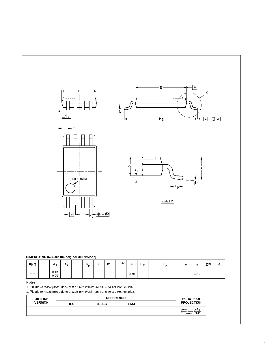
VSOP-8A: plastic small outline package; 8 leads; body width 4.4 mm
1.35
1.15
A
1.15
0.23
0.21
0.16
0.10
3.4
2.8
4.6
4.2
6.7
6.1
0.7
0.3
0.12
0.875
max.
10
∞
0
∞
VSOP-8A

Philips Semiconductors
Product data
SA57005
Multiple output low noise, low dropout linear regulator
2002 Jun 20
11
NOTES

Philips Semiconductors
Product data
SA57005
Multiple output low noise, low dropout linear regulator
2002 Jun 20
12
Definitions
Short-form specification -- The data in a short-form specification is extracted from a full data sheet with the same type number and title. For
detailed information see the relevant data sheet or data handbook.
Limiting values definition -- Limiting values given are in accordance with the Absolute Maximum Rating System (IEC 60134). Stress above one
or more of the limiting values may cause permanent damage to the device. These are stress ratings only and operation of the device at these or
at any other conditions above those given in the Characteristics sections of the specification is not implied. Exposure to limiting values for extended
periods may affect device reliability.
Application information -- Applications that are described herein for any of these products are for illustrative purposes only. Philips
Semiconductors make no representation or warranty that such applications will be suitable for the specified use without further testing or
modification.
Disclaimers
Life support -- These products are not designed for use in life support appliances, devices or systems where malfunction of these products can
reasonably be expected to result in personal injury. Philips Semiconductors customers using or selling these products for use in such applications
do so at their own risk and agree to fully indemnify Philips Semiconductors for any damages resulting from such application.
Right to make changes -- Philips Semiconductors reserves the right to make changes, without notice, in the products, including circuits, standard
cells, and/or software, described or contained herein in order to improve design and/or performance. Philips Semiconductors assumes no
responsibility or liability for the use of any of these products, conveys no license or title under any patent, copyright, or mask work right to these
products, and makes no representations or warranties that these products are free from patent, copyright, or mask work right infringement, unless
otherwise specified.
Contact information
For additional information please visit
http://www.semiconductors.philips.com.
Fax: +31 40 27 24825
For sales offices addresses send e-mail to:
sales.addresses@www.semiconductors.philips.com.
©
Koninklijke Philips Electronics N.V. 2002
All rights reserved. Printed in U.S.A.
Date of release: 08-02
Document order number:
9397 750 10161
Philips
Semiconductors
Data sheet status
[1]
Objective data
Preliminary data
Product data
Product
status
[2]
Development
Qualification
Production
Definitions
This data sheet contains data from the objective specification for product development.
Philips Semiconductors reserves the right to change the specification in any manner without notice.
This data sheet contains data from the preliminary specification. Supplementary data will be
published at a later date. Philips Semiconductors reserves the right to change the specification
without notice, in order to improve the design and supply the best possible product.
This data sheet contains data from the product specification. Philips Semiconductors reserves the
right to make changes at any time in order to improve the design, manufacturing and supply.
Changes will be communicated according to the Customer Product/Process Change Notification
(CPCN) procedure SNW-SQ-650A.
Data sheet status
[1] Please consult the most recently issued data sheet before initiating or completing a design.
[2] The product status of the device(s) described in this data sheet may have changed since this data sheet was published. The latest information is available on the Internet at URL
http://www.semiconductors.philips.com.