Document Outline
- GENERAL DESCRIPTION
- FEATURES
- APPLICATIONS
- SIMPLIFIED SYSTEM DIAGRAM
- ORDERING INFORMATION
- PIN CONFIGURATION
- PIN DESCRIPTION
- MAXIMUM RATINGS
- ELECTRICAL CHARACTERISTICS
- TYPICAL PERFORMANCE CURVES
- TECHNICAL DISCUSSION
- APPLICATION INFORMATION
- PACKING METHOD
- PACKAGE OUTLINE
- REVISION HISTORY
- Data sheet status
- Definitions
- Disclaimers
Philips
Semiconductors
SA57254-XX
CMOS switching regulator
(PWM controlled)
Product data
Supersedes data of 2001 Aug 01
2003 Nov 11
INTEGRATED CIRCUITS

Philips Semiconductors
Product data
SA57254-XX
CMOS switching regulator (PWM controlled)
2
2003 Nov 11
GENERAL DESCRIPTION
The SA57254-XX is a fully integrated DC/DC converter circuit.
Efficient, compact power conversion is achieved with a pulse width
modulation (PWM) controlled switching regulator circuit designed
using CMOS processing. Low ripple and high efficiency of typically
83% are achieved through PWM control. The regulator has a high
precision output with
±
2.4% accuracy. Few external components are
required.
The SA57254-XX has a built-in soft-start circuit which reduces
inrush current and voltage overshoot during start-up. A low
resistance CMOS power FET, which has low leakage current and
low parasitic capacitance, is on-chip.
FEATURES
∑
Operates from 0.7 to 9 V
DC
∑
Ultra low operating supply current--typically 17
µ
A
∑
Built-in power FET
∑
High efficiency--typically 83%
∑
High precision output--typically
±
2.4%
∑
Operating temperature range of ≠40 to +85
∞
C
∑
Available output voltages: 2.0, 2.5, 2.8, 3.0, 3.3, 3.6, 5.0 V
DC
∑
Available in a 5-lead small outline surface mount package
(SOP003)
APPLICATIONS
∑
Mobile and portable phones
∑
Instrumentation and industrial products
∑
Other portable, battery-operated equipment
SIMPLIFIED SYSTEM DIAGRAM
SL01501
1
V
REF
5
4
V
OUT
V
BATT
SA57254-XX
GND
SW
FB
PWM CONTROL
SOFT START
2
R
R
SA57254-XX as a boost (step-up) converter.
V
DD
Figure 1. Simplified system diagram.

Philips Semiconductors
Product data
SA57254-XX
CMOS switching regulator (PWM controlled)
2003 Nov 11
3
ORDERING INFORMATION
TYPE NUMBER
PACKAGE
TEMPERATURE
TYPE NUMBER
NAME
DESCRIPTION
VERSION
RANGE
SA57254-XXGW
SOT23-5,
SOT25, SO5
Plastic small outline package; 5 leads; body width 1.6 mm
SOP003
≠40 to +85
∞
C
NOTE:
The device has seven voltage output options, indicated by the XX
on the Type Number.
XX
VOLTAGE (Typical)
20
2.0 V
25
2.5 V
28
2.8 V
30
3.0 V
33
3.3 V
36
3.6 V
50
5.0 V
Part number marking
Each device is marked with a four letter code. The first three letters
designate the product. The fourth letter, represented by `x', is a date
tracking code.
Part number
Marking
SA57254-20GW
A E K x
SA57254-25GW
A E L x
SA57254-28GW
A E M x
SA57254-30GW
A E N x
SA57254-33GW
A E P x
SA57254-36GW
A E R x
SA57254-50GW
A E S x
PIN CONFIGURATION
SL01502
1
2
3
4
5
SW
GND
N/C
V
DD
FB
SA57254-XX
Figure 2. Pin configuration.
PIN DESCRIPTION
PIN
SYMBOL
DESCRIPTION
1
FB
Feedback from the output voltage to the PWM
control.
2
V
DD
Voltage input to regulator.
3
N/C
No connection.
4
GND
Ground.
5
SW
Switching output to inductor.
MAXIMUM RATINGS
SYMBOL
PARAMETER
MIN.
MAX.
UNIT
V
IN(max)
Power supply voltage
≠0.3
11
V
V
FB
FB pin voltage
≠0.3
11
V
V
SW
SW pin voltage
≠0.3
11
V
I
SW
SW pin current
≠
300
mA
T
oper
Operating temperature
≠40
+85
∞
C
T
stg
Storage temperature
≠40
+125
∞
C
P
D
Power dissipation
≠
150
mW
Philips Semiconductors
Product data
SA57254-XX
CMOS switching regulator (PWM controlled)
2003 Nov 11
4
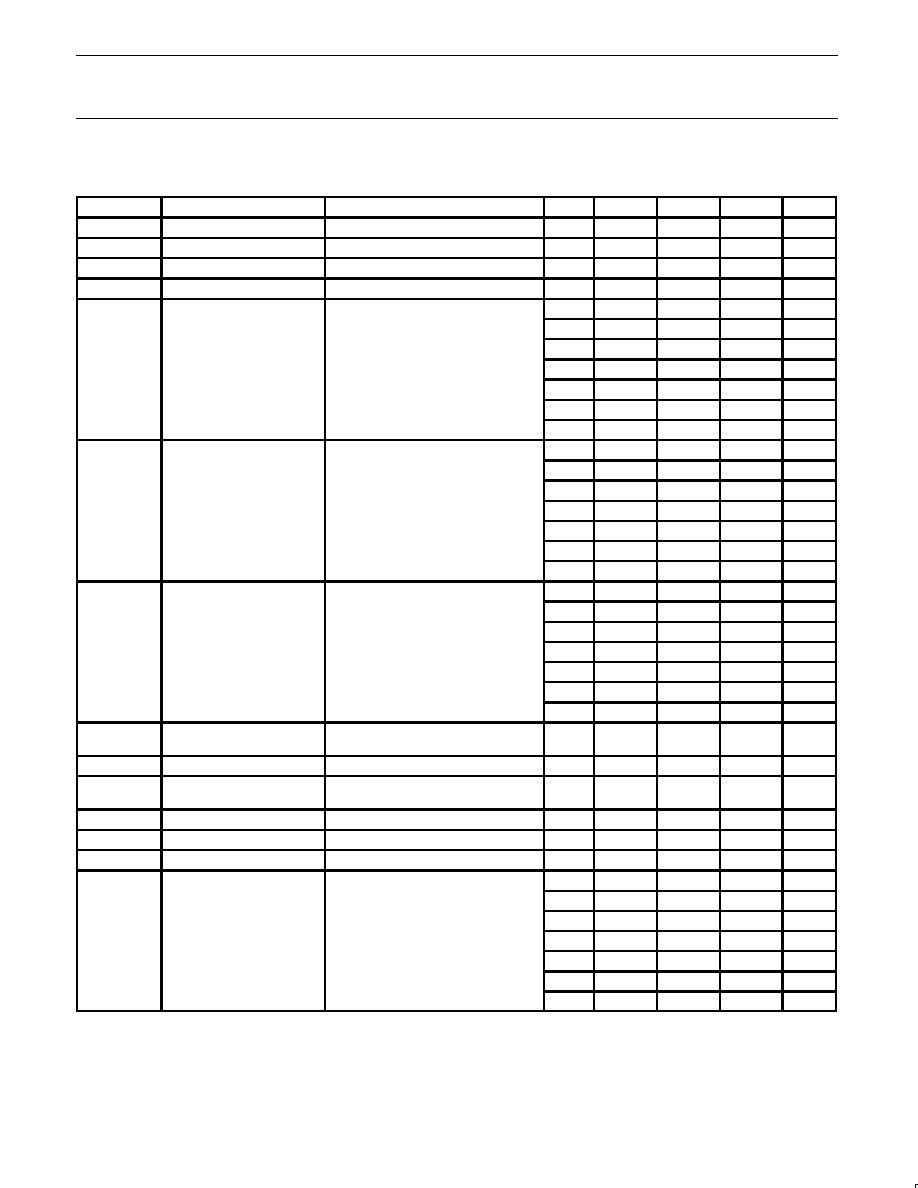
ELECTRICAL CHARACTERISTICS
T
amb
= 25
∞
C, unless otherwise specified.
SYMBOL
PARAMETER
CONDITIONS
Part #
MIN.
TYP.
MAX.
UNIT
V
IN
input voltage
≠
≠
≠
9.0
V
V
ST1
operating start voltage
I
OUT
= 1.0 mA
≠
≠
≠
0.9
V
V
ST2
oscillator start voltage
≠
≠
≠
0.8
V
V
HLD
operation hold voltage
I
OUT
= 1.0 mA
≠
0.7
≠
≠
V
I
SS1
consumption current 1
V
OUT
= output voltage
◊
0.95
-20
≠
11.6
19.4
µ
A
-25
≠
14.3
23.9
µ
A
-28
≠
16.1
26.8
µ
A
-30
≠
17.2
28.7
µ
A
-33
≠
19.1
31.8
µ
A
-36
≠
22.4
37.3
µ
A
-50
≠
38.5
64.1
µ
A
I
SS2
consumption current 2
V
OUT
= output voltage + 0.5 V
-20
≠
3.1
6.2
µ
A
-25
≠
3.2
6.3
µ
A
-28
≠
3.2
6.4
µ
A
-30
≠
3.2
6.4
µ
A
-33
≠
3.3
6.5
µ
A
-36
≠
3.3
6.5
µ
A
-50
≠
3.5
6.9
µ
A
R
DS(ON)
internal switch-on resistance
V
SW
= 0.4 V
-20
≠
5.6
8.9
(
)
-25
≠
4.1
6.5
-28
≠
4.1
6.5
-30
≠
3.2
5.1
-33
≠
3.2
5.1
-36
≠
3.2
5.1
-50
≠
2.2
3.5
I
SWO
switching transistor leak
current
V
OUT
= V
SW
= 9 V
≠
≠
≠
1.0
µ
A
V
OUT2
load ripple voltage
I
OUT
= 10 mA
I
OUT
(following)
◊
1.25
≠
≠
30
60
mV
V
OUT
/
T
amb
output voltage temperature
coefficient
≠40
∞
C
T
amb
+85
∞
C
≠
≠
±
50
≠
ppm/
∞
C
f
OSC
oscillator frequency
V
OUT
= output voltage
◊
0.95
≠
42.5
50
57.5
kHz
MaxDuty
maximum duty ratio
V
OUT
= output voltage
◊
0.95
≠
75
83
90
%
t
SS
soft start time
I
OUT
= 1.0 mA
≠
3.0
6.0
12
ms
E
FFI
efficiency
-20
≠
75
≠
%
-25
≠
79
≠
%
-28
≠
79
≠
%
-30
≠
83
≠
%
-33
≠
83
≠
%
-36
≠
83
≠
%
-50
≠
87
≠
%

Philips Semiconductors
Product data
SA57254-XX
CMOS switching regulator (PWM controlled)
2003 Nov 11
5
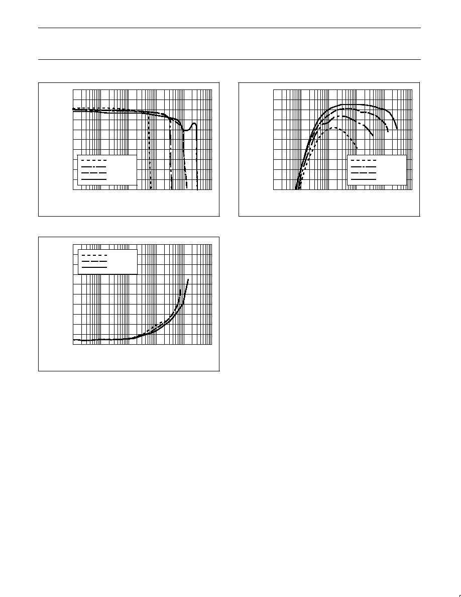
TYPICAL PERFORMANCE CURVES
SL01456
T
amb
∞
C)
50
40
30
20
10
0
≠40
≠20
0
20
40
60
80
100
V
OUT
= OUTPUT VOLTAGE
◊
0.95
I
SS1
(
µ
A)
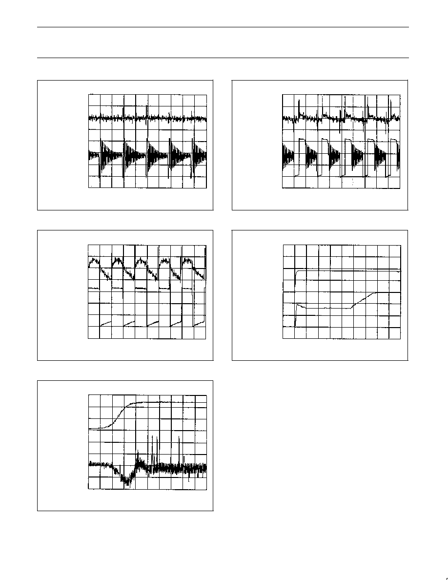
Figure 3. Supply current 1 versus temperature.
SL01457
T
amb
∞
C)
5
4
3
2
1
0
≠40
≠20
0
20
40
60
80
100
V
OUT
= OUTPUT VOLTAGE + 0.5 V
I
SS2
(
µ
A)
Figure 4. Supply current 2 versus temperature.
SL01458
T
amb
∞
C)
55
50
45
40
35
30
≠40
≠20
0
20
40
60
80
100
V
OUT
= OUTPUT VOLTAGE
◊
0.95
70
65
60
f
OSC
(kHz)
Figure 5. Oscillator frequency versus temperature.
SL01459
V
OUT
(V)
50
40
30
20
10
0
0
2
4
6
8
10
T
amb
= 25
∞
C
I
SS1, 2
(
µ
A)
Figure 6. Supply current 1, 2 versus V
OUT
.
SL01462
V
OUT
(V)
250
200
150
100
50
0
0
1
2
3
4
5
T
amb
= 25
∞
C
V
CONT
= 0.4 V
I
SW
(mA)
Figure 7. Typical switch current versus V
OUT
.
SL01471
V
OUT
(V)
50
40
30
0
1
2
3
4
5
70
60
T
amb
= 25
∞
C
f
OSC
(kHz)
Figure 8. Oscillator frequency versus V
OUT
.
Philips Semiconductors
Product data
SA57254-XX
CMOS switching regulator (PWM controlled)
2003 Nov 11
6
V
OUT
OUTPUT VOLTAGE
(20 mV/div)
V
SW
SW VOLTAGE
(1 V/div)
t (10
µ
s/div)
SL01472
V
IN
= 1.8 V
Figure 9. Ripple voltage at I
OUT
= 200
µ
A.
V
OUT
OUTPUT VOLTAGE
(20 mV/div)
V
SW
SW VOLTAGE
(1 V/div)
t (10
µ
s/div)
SL01473
V
IN
= 1.8 V
Figure 10. Ripple voltage at I
OUT
= 10 mA.
V
OUT
OUTPUT VOLTAGE
(20 mV/div)
V
SW
SW VOLTAGE
(1 V/div)
t (10
µ
s/div)
SL01474
V
IN
= 1.8 V
Figure 11. Ripple voltage at I
OUT
= 60 mA.
V
IN
INPUT VOLTAGE
(1 V/div)
V
OUT
OUTPUT VOLTAGE
(1 V/div)
t (1 ms/div)
SL01475
I
OUT
= 60 mA
Figure 12. Start-up characteristic V
IN
: 0 V
1.8 V.
I
OUT
LOAD CURRENT
(20 mA/div)
V
OUT
OUTPUT VOLTAGE
(50 mV/div)
t (200
µ
s/div)
SL01477
I
OUT
: 100
µ
A
50 mA; V
IN
= 1.8 V
Figure 13. Output load regulation, increasing current.
Philips Semiconductors
Product data
SA57254-XX
CMOS switching regulator (PWM controlled)
2003 Nov 11
7
I
OUT
LOAD CURRENT
(20 mA/div)
V
OUT
OUTPUT VOLTAGE
(50 mV/div)
t (5 ms/div)
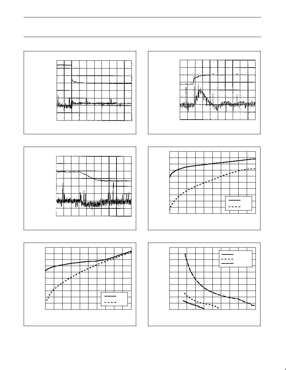
SL01478
I
OUT
: 50 mA
100
µ
A; V
IN
= 1.8 V
Figure 14. Output load regulation, decreasing current.
V
IN
INPUT VOLTAGE
(500 mV/div)
V
OUT
OUTPUT VOLTAGE
(50 mV/div)
t (100
µ
s/div)
SL01479
V
IN
: 1.8 V
2.4 V; I
OUT
= 50 mA
Figure 15. Input line regulation, increasing voltage.
V
IN
INPUT VOLTAGE
(500 mV/div)
V
OUT
OUTPUT VOLTAGE
(50 mV/div)
t (200
µ
s/div)
SL01480
V
IN
: 2.4 V
1.8 V; I
OUT
= 50 mA
Figure 16. Input line regulation, decreasing voltage.
SL01481
I
OUT
, OUTPUT CURRENT (mA)
0
1
2
3
4
5
6
7
8
9
10
V
IN
, INPUT
VOL
T
AGE
(V)
0.0
0.1
0.2
0.3
0.4
0.5
0.6
0.7
0.8
0.9
1.0
V
ST1
V
DO
Figure 17. Output current versus starting voltage.
SL01482
I
OUT
, OUTPUT CURRENT (mA)
0
1
2
3
4
5
6
7
8
9
10
V
IN
, INPUT
VOL
T
AGE
(V)
0.0
0.1
0.2
0.3
0.4
0.5
0.6
0.7
0.8
0.9
1.0
V
ST1
V
DO
Figure 18. Input voltage versus output current.
SL01483
V
IN
, INPUT VOLTAGE (V)
0.0
0.5
1.0
1.5
2.0
2.5
3.0
3.5
4.0
4.5
5.0
I
IN
,
INPUT
CURRENT
(
A)
0
50
100
150
200
250
300
350
400
450
500
V
OUT
= 2 V
V
OUT
= 3 V
µ
V
OUT
= 5 V
Figure 19. Input voltage versus supply current.
Philips Semiconductors
Product data
SA57254-XX
CMOS switching regulator (PWM controlled)
2003 Nov 11
8
SL01484
I
OUT
, OUTPUT CURRENT (mA)
0.01
0.1
1
10
100
1000
4.90
4.92
4.94
4.96
4.98
5.00
5.02
5.04
5.06
5.08
5.10
V
OUT
, OUTPUT
VOL
T
AGE
(V)
V
IN
= 0.9 V
V
IN
= 1.8 V
V
IN
= 3.0 V
V
IN
= 4.0 V
Figure 20. Output current versus voltage (100
µ
H inductor).
SL01485
I
OUT
, OUTPUT CURRENT (mA)
0.01
0.1
1
10
100
1000
50
55
60
65
70
75
80
85
90
95
100
E
FFI
, EFFICIENCY
(%)
V
IN
= 0.9 V
V
IN
= 1.8 V
V
IN
= 3.0 V
V
IN
= 4.0 V
Figure 21. Output current versus efficiency (100
µ
H inductor).
SL01486
I
OUT
, OUTPUT CURRENT (mA)
0.01
0.1
1
10
100
1000
0
10
20
30
40
50
60
70
80
90
100
V
R
, RIPPLE VOL
T
AGE (mV)
V
IN
= 0.9 V
V
IN
= 1.8 V
V
IN
= 2.4 V
Figure 22. Output current versus ripple voltage
(L
0
= 100
µ
H; C
OUT
= 33
µ
F).

Philips Semiconductors
Product data
SA57254-XX
CMOS switching regulator (PWM controlled)
2003 Nov 11
9
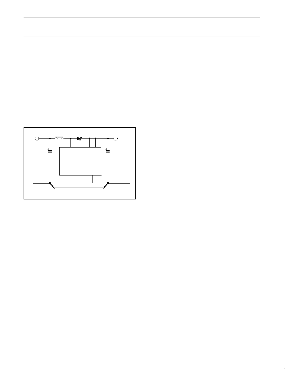
TECHNICAL DISCUSSION
General discussion
The SA57254-XX is a highly integrated boost-mode switching power
supply integrated circuit. Each device is set to provide a fixed output
voltage by having a fully compensated internal voltage feedback
loop. The SA57254-XX operates at a fixed frequency of 50 kHz and
can operate from a single alkaline cell (0.9 V) or up to 9 V.
The SA57254-XX has an internal common-source power switching
MOSFET which provides the PWM signal to the inductor. The
voltage error amplifier for maintaining a fixed output voltage, the
oscillator and a PWM generator are all in the package.
SL01503
1
V
REF
5
4
SA57254-XX
GND
SW
FB
PWM CONTROL
SOFT START
R
R
V
DD
2
Figure 23. Functional diagram.

Philips Semiconductors
Product data
SA57254-XX
CMOS switching regulator (PWM controlled)
2003 Nov 11
10
APPLICATION INFORMATION
The SA57254-XX can be used for a simple boost (step-up)
converter or the less commonly used flyback converter (isolated
boost). The major operating restriction of the simple boost converter
is that its output voltage must always be above the highest
expected value of the input voltage. The flyback converter circuit
requires more parts, but the output voltage is not restricted by the
input voltage.
Boost converter fundamentals
The boost or step-up converter is a non-dielectrically isolated
switching power supply topology (arrangement of power parts). That
is, the input power source is directly connected to the output load
(ground and signals). A typical boost converter, with an optional
passive snubber, can be seen in Figure 24.
To understand the boost converter's operation, examine its three
periods of operation. These periods are: the power switch on-time
(period 1); the inductor discharge period (period 2); and the inductor
empty state (period 3). These periods and their associated currents
can be seen in Figure 25.
SL01504
D
V
IN
C
IN
GND
SA57254-XX
SW
V
DD
PASSIVE SNUBBER
(OPTIONAL)
V
OUT
C
OUT
FB
L
0
Figure 24. Boost converter.
SL01464
SWITCH VOLTAGE (V)
INDUCTOR CURRENT (A)
0
V
IN
(V
IN
≠ V
OUT
)
I
peak
I
SW
◊
R
DS(ON)
CORE EMPTY,
PARASITIC CIRCULATING ENERGY
+V
OUT
ENERGY BEING TRANSFERRED TO OUTPUT
SPIKE
ENERGY BEING
STORED IN INDUCTOR
+V
IN
L
0
L
0
PERIOD 1
PERIOD 2
PERIOD 3
Figure 25. Boost converter waveforms (discontinuous mode).

Philips Semiconductors
Product data
SA57254-XX
CMOS switching regulator (PWM controlled)
2003 Nov 11
11
Period 1: power switch on-time
During this period, a simple circuit loop is formed when the power
switch is on. The input voltage source is connected directly across
the boost inductor (L
0
). A current ramp is exhibited whose slope is
described by:
IL
(
on)
+
V
IN
L
0
Eqn. (1)
Energy is then stored within the core material of the inductor and is
described by:
E
sto
+
0.5
L
0
I
peak
2
Eqn. (2)
This current ramp continues until the controller turns off the power
switch.
Period 2: inductor discharge period
The instant the power switch turns off, the current flowing through
the inductor forces the voltage at its output node (switched node) to
rise quickly above the input voltage (spike). This voltage is then
clamped when it exceeds the device's output voltage and the output
rectifier becomes forward biased. The inductor empties its stored
energy in the form of a linearly decreasing current ramp whose
slope is dictated by:
I
L(off)
[
V
IN
*
V
OUT
L
0
Eqn. (3)
The stored energy is transferred to the output capacitor. This output
current continues until the magnetic core is completely emptied of its
stored energy or the power switch turns back on.
Period 3: inductor empty state
D
ISCONTINUOUS
MODE
--This period as displayed in Figure 25 occurs
in the discontinuous≠mode of operation of a boost converter. It is
identified by a period of "ringing" following the output period
(period 2). The inductor has been completely emptied of its stored
energy and the switched node returns to the level of the input
voltage. Ringing is seen at this node because a resonant circuit is
formed by the inductance of L
0
and any parasitic inductances and
capacitances connected to that node. This ringing has very little
energy and can easily be eliminated by a small passive snubber.
C
ONTINUOUS
MODE
--If the inductor is not completely emptied of its
stored energy before the power switch turns on again, the converter
is operating in the continuous mode. A small amount of residual flux
(energy) remains in the inductor core and the current waveform
jumps to an initial value when the power switch is again turned-on.
This mode offers some advantages over the discontinuous-mode,
because the peak current seen by the power switch is lower. In low
voltage applications, the inductor can store more energy with lower
peak currents.
The continuous mode waveforms can be seen in Figure 26.
SWITCH VOLTAGE (V)
INDUCTOR CURRENT (A)
0
SPIKE
+V
OUT
+V
IN
V
IN
(V
IN
≠ V
OUT
)
I
peak
RESIDUAL FLUX
ENERGY BEING
TRANSFERRED
TO OUTPUT
ENERGY BEING
STORED IN
INDUCTOR
SL01465
L
0
L
0
Figure 26. Continuous mode waveforms.

Philips Semiconductors
Product data
SA57254-XX
CMOS switching regulator (PWM controlled)
2003 Nov 11
12
Determining the value of the boost inductor
The precise value of the boost inductor is not critical to the operation
of the SA57254-XX. The value of the boost inductor should be
calculated to provide continuous-mode operation over most of its
operating range. The converter may enter the discontinuous-mode
when the output load current falls to less than about 20 percent of
the full-load current.
At low input voltages, the time required to store the needed energy
lengthens, but the time needed to empty the inductor's core of its
energy shrinks. Conversely, at high input voltages, the time needed
to store the energy shrinks while the time needed to empty the core
increases. See Equations (1) and (3). At the extremes of these
conditions, the converter will fall out of regulation, that is the output
voltage will begin to fall, because the time needed for either storing
or emptying the stored inductor energy is too short to support the
output load current.
To determine the nominal value of the inductance, use Equation (4).
L
0
^
V
IN(min)
T
on
I
peak
Eqn. (4)
Where:
V
IN(min)
is the lowest expected input operating voltage (V).
T
on
is about 10
µ
s or one-half the switching period (s).
I
peak
is the maximum peak current for the SA57254-XX (0.3 A).
This is an estimated inductor value and you can select an
inductance value slightly higher or lower with little effect on the
converter's operation. If the design falls out of regulation within the
desired operating range, reduce the inductance value, but by no
more than 30 percent.
Determining the minimum value of the capacitors
The input and output capacitors experience the current waveforms
seen in Figures 25 and 26. The peak currents can be typically
between 3 to 6 times the average currents flowing into the input and
from the output. This makes the choice of capacitor an issue of how
much ripple voltage can be tolerated on the capacitor's terminals
and how much heating the capacitor can tolerate. At the power
levels produced by the SA57254-XX heating is not a major issue.
The Equivalent Series Resistance (ESR) of the capacitor, the
resistance that appears between its terminals, and the actual
capacitance causes heat to be generated within the case whenever
there is current entering or exiting the capacitor. ESR also adds to
the apparent voltage drop across the capacitor. The heat that is
generated can be approximated by Equation (5).
P
D
(
in watts)
^
(1.8
I
av
)
2
(
R
ESR
)
Eqn. (5)
ESR's effect on the capacitor voltage is given by Equation (6).
D
V
C
^
I
peak
(
R
ESR
)
Eqn. (6)
(expressed as V
p≠p
)
A ceramic capacitor would typically be used in this application if the
required value is less than 1 ≠ 10
µ
F, or a tantalum capacitor for
required values of 10
µ
F and above. Lower cost aluminum electrolytic
capacitors can be used, but you should confirm that the higher ESRs
typically exhibited by these capacitors does not cause a problem.
The minimum value of the output capacitor can be estimated by
Equation (7).
C
OUT
u
(
I
OUT(max)
) (
T
off
)
V
ripple(p
*
p)
Eqn. (7)
Where:
I
OUT
is the average value of the output load current (A).
T
off
is the nominal off≠time of the power switch (sec) [
10
µ
s].
V
ripple
is the desired amount of ripple voltage (V
p≠p
).
Finding the value of the input capacitor is done by Equation (8).
C
IN
u
(
I
peak
) (
T
on
)
V
drop
Eqn. (8)
Where:
I
peak
is the expected maximum peak current of the switch (A).
T
on
is the on-time of the switch (sec) [
10
µ
s].
V
drop
is the desired amount of voltage drop across the capacitor
(V
p≠p
).
These calculations should produce a good estimate of the needed
values of the input and output capacitors to yield the desired ripple
voltages.
Selecting the output rectifier
The output rectifier (D) is critical to the efficiency and low-noise
operation of the boost converter. The majority of the loss within the
supply will be caused by the output rectifier. Three parameters are
important in the rectifier's operation within a boost-mode supply.
These are defined below.
Forward voltage drop (V
f
)--This is the voltage across the rectifier
when a forward current is flowing through the rectifier. A P-N
ultra-fast diode exhibits a 0.7 ≠ 1.4 volt drop, and this drop is
relatively fixed over the range of forward currents. A Schottky diode
exhibits a 0.3 ≠ 0.6 volt drop and appears more resistive during the
forward conduction periods. That is, its forward voltage drop
increases with increasing currents. You can gain an advantage by
purposely over-rating the current rating of a Schottky rectifier to
minimize this increasing voltage drop.
Reverse recovery time (T
rr
)--This is an issue when the boost
supply is operating in the continuous-mode. T
rr
is the amount of time
required for the rectifier to assume an open circuit when a forward
current is flowing and a reverse voltage is then placed across its
terminals. P-N ultra-fast rectifiers typically have a 25≠40 ns reverse
recovery time. Schottky rectifiers have a very short or no reverse
recovery time.
Forward recovery time (T
fr
)--This is the amount of time before a
rectifier begins conducting forward current after a forward voltage is
placed across its terminals. This parameter is not always well
specified by the rectifier manufacturers. It causes a spike to appear
when the power switch turns off. This particular point in its operation
causes the most radiated noise. Several rectifiers may have to be
evaluated for the prototype. After the final output rectifier selection is
made, if the spike is still causing a problem a small passive snubber
can be placed across the rectifier.
For this boost application, the best choice of output rectifier is a low
forward drop, 0.5 ≠ 1 ampere, 20 volt Schottky rectifier such as the
Philips part number BAT120A.

Philips Semiconductors
Product data
SA57254-XX
CMOS switching regulator (PWM controlled)
2003 Nov 11
13
Flyback converter
The SA57254-XX can also be used to create a flyback converter,
also known as an isolated boost converter. The advantage of a
flyback converter is that the input voltage can go higher or lower
than the output voltage without affecting the operation of the
converter. The only restrictions are the peak current flowing into the
switch pin (SW) and the breakdown voltage of the SW and feedback
(V
FB
) pins.
One transformer can accommodate a variety of output voltages in
different applications, because the circuit will change the on and
off≠times to provide the desired output voltage.
The output voltage of the flyback can be changed by using a
SA57254-XX with the desired output voltage, with no other changes
to the circuit.
Selecting the components
It is best to operate the transformer in the continuous-mode where
the highest expected peak primary current is below the maximum
current rating of the SA57254-XX switch.
Because the SA57254-XX is a peak current-limitied IC, begin with a
peak current equal to or less than the maximum current rating of the
part (0.3 A). A reasonable value of the primary inductance can be
found in Equation (9).
L
pri
t
5
V
IN(min)
T
on
I
peak
Eqn. (9)
Where:
I
peak
is 0.3 A or less.
T
on
is the maximum expected on-time of the switch (
10
µ
s).
V
IN(min)
is the lowest expected input voltage (V).
Then select an off-the-shelf transformer such as the Coiltronics
CTX100≠1P, a 1:1 turns ratio transformer that has a primary
inductance of 100
µ
H. It does not reach saturation until the primary
current reaches 440 mA, which is above the expected peak current
of the flyback converter. The 1:1 turns ratio should work for output
voltages from 0.8 to 2 times the highest input voltage, and produce
the output voltage set by the SA57254-XX. The only other restriction
is that the input voltage plus the output voltage must be less than
the breakdown voltage of the SA57254-XX (9 V).
Use Equation (8) to determine the minimum value for the input
capacitor. A 0.1 V drop is desired across this capacitor.
C
IN
u
(0.3
A) (10
m
s)
0.1
V
+
30
m
F
A 47
µ
F at 6 V tantalum capacitor would be suitable.
For the design example, the output voltage will be +3.3 V with a
maximum output current of 50 mA. The input voltage can vary
between +1.8 V and 4.0 V. The design can be seen in Figure 27,
and the expected waveforms can be seen in Figure 28.
SL01505
SA57254-33
V
BATT
47
µ
F
@ 10 V
GND
FB
SW
47
µ
F
@ 10 V
V
OUT
3.3 V
@ 0.1 A
COILTRONICS
CTX100-1P
Figure 27. Flyback converter circuit.
SL01468
DIODE CURRENT (A)
SWITCH CURRENT (A)
SWITCH
VOLTAGE
(V)
SECONDARY VOLTAGE (V)
V
IN
+ V
OUT
(1:1 TRANSFORMER)
+V
OUT
GROUND (0 V)
≠V
IN
I
SW(peak)
I
diode(peak)
V
IN
I
peak
= I
diode
(1:1 TRANSFORMER)
V
IN
Figure 28. Flyback converter waveforms.

Philips Semiconductors
Product data
SA57254-XX
CMOS switching regulator (PWM controlled)
2003 Nov 11
14
Designing a passive snubber
If the switching power supply is generating too much radio
frequency interference (RFI) a passive snubber can be added.
A passive snubber is a series resistor and capacitor placed across
any component that exhibits a resonant "ringing". This series R-L-C
loop creates a lossy or damped tank circuit that dissipates the
ringing energy. The design is critical, because it introduces another
loss within the converter.
Designing a snubber is an empirical process, mainly because it
involves undefined parasitic capacitances and inductances
contributed by the PCB layout, leakage inductance, and device
capacitances. The snubber should be placed across the major
source of the spike or ringing which is the output rectifier for a boost
converter (see Figure 24) and the primary winding of the transformer
for a flyback transformer.
The usual design process is:
1. Measure the period of the undesired ringing (T
0
).
2. Place a very small ceramic capacitor (about 10 pF) across the
output rectifier or primary winding.
3. Re-measure the period of the undesired ringing. The new period
should be about 3 times that of T
0
. If it is less than this, place a
slightly larger value of capacitor across the output rectifier or
primary winding.
4. Once the desired increase in the ringing period is achieved with
a capacitance (C
0
), place a resistor in series with the capacitor
whose value is approximately:
R
snubber
^
T
0
2
p
C
0
Eqn. (10)
This should produce a snubber that does not load the circuit and
introduces a very small loss.
SL01506
SA57254-XX
V
BATT
GND
FB
SW
V
OUT
R
PASSIVE SNUBBER
V
DD
Figure 29. Flyback converter with passive snubber.
Philips Semiconductors
Product data
SA57254-XX
CMOS switching regulator (PWM controlled)
2003 Nov 11
15
Laying out the printed circuit board
The design of the printed circuit board (PCB) is critical to the proper
operation of all switching power supplies. Its design affects the
supply stability, radio frequency interference behavior and the
reliability of the converter.
Never use the autoroute feature of any PCB design program
because this will always produce traces that are too long and too
thin.
The input and output capacitors are the only source or sink of the
high frequency currents found in a switching power supply. All
connections to the switching power supply from the outside circuits
should be made to the input or output capacitor terminals (+ and ≠).
Internally, the layout should adhere to a "one-point" grounding
system, as shown in Figure 30.
SL01507
V
IN
C
IN
GND
SA57254-XX
SW
FB
V
OUT
C
OUT
OUTPUT
GROUND
TO ONE POINT
INPUT
GROUND
TO ONE POINT
V
DD
L
0
Figure 30. Grounding trace for converter.
The traces between the input and output capacitors and the
inductor, power switch and rectifier(s) should be as short and wide
as possible. This reduces the series resistance and inductance that
can be introduced by traces.
The guidelines for a PCB layout can be summarized as:
∑
The traces between the input and output capacitor to the inductor,
power switch and the rectifier should be made as short and as
wide as possible.
∑
Strictly adhere to the one-point wiring practices shown in
Figure 30.
∑
On a 2-sided board, do not run sensitive signals traces under the
AC voltage node.
∑
The IC (control) ground is terminated at the output capacitor's
negative terminal.
Designing the PCB for effective heat dissipation
The maximum junction temperature is +125
∞
C, which should not be
exceeded under any operating conditions. Designing a PCB that
includes a heatsink system under the device is the key to cooler
operation of the circuit, and the long≠term reliable operation of the
converter.
The major sources of heat within the converter are the power switch
inside the SA57254-XX, the resistive losses within the inductor, and
losses associated with the output rectifier. These losses can be
estimated by the following equations:
Power switch:
P
D(sw)
^
T
ON
I
PK
2
R
DS(ON)
f
SW
Eqn. (11)
Inductor:
P
D(L0)
^
I
pk
2
R
winding
Eqn. (12)
Output rectifier:
P
D(rect)
^
I
OUT(Vfwd)
Eqn. (13)
The thermal resistance (R
th(j-a)
) of the SA57254-XX is approximately
220
∞
C/W, assuming the device is soldered to a 2 oz. copper FR4
fiberglass circuit board, and that the minimum footprint was used
(copper just under the leads). A rule of thumb in PCB design is that
the thermal resistance can be reduced by 30% for each doubling of
the copper area close to the device. This effect diminishes for areas
greater than five times the minimum PCB footprint. If you take
advantage of this rule, thermal resistance can be reduced by using
wide copper lands when connecting to the leads of the major
power-producing parts. These PCB traces should almost fill the
areas surrounding the converter parts to conduct heat away from
the device. For demanding applications, additional heat dissipation
area can be created by placing a copper island on the opposite side
of the PCB from each wide trace and connecting it to the trace with
vias (plated thru holes).
The junction temperature can be estimated by Equation (14).
T
j
^
(
P
D
R
th(j-a)
)
)
T
amb(max)
Eqn. (14)
Where:
P
D
is the power dissipation (W).
R
th(j-a)
is the effective thermal resistance with the additional
copper (
∞
C/W).
T
amb
is the highest local expected ambient temperature (
∞
C).
Philips Semiconductors
Product data
SA57254-XX
CMOS switching regulator (PWM controlled)
2003 Nov 11
16
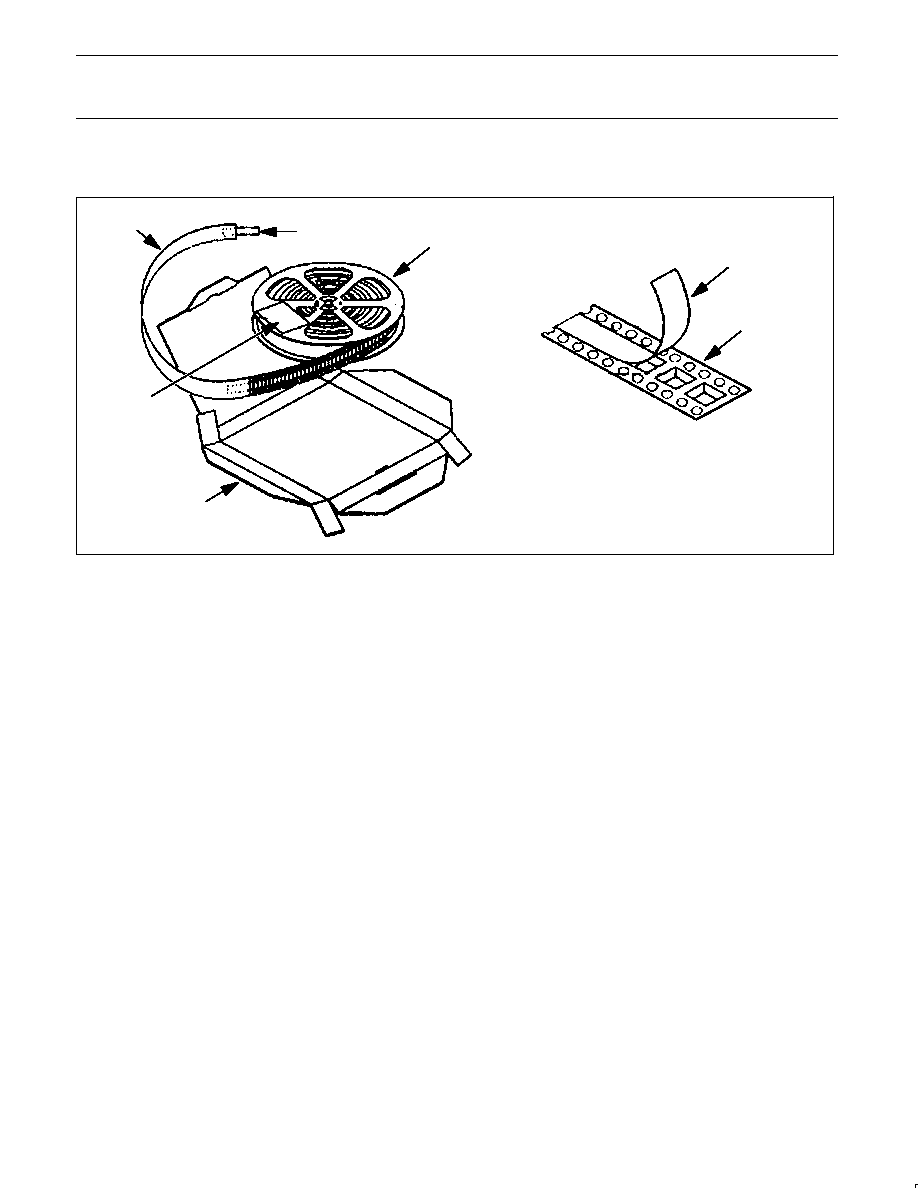
PACKING METHOD
The SA57254-XX is packed in reels, as shown in Figure 31.
SL01305
TAPE DETAIL
COVER TAPE
CARRIER TAPE
REEL
ASSEMBLY
TAPE
GUARD
BAND
BARCODE
LABEL
BOX
Figure 31. Tape and reel packing method.

Philips Semiconductors
Product data
SA57254-XX
CMOS switching regulator (PWM controlled)
2003 Nov 11
17
Plastic small outline package; 5 leads; body width 1.6 mm
SOP003
Philips Semiconductors
Product data
SA57254-XX
CMOS switching regulator (PWM controlled)
2003 Nov 11
18
REVISION HISTORY
Rev
Date
Description
_2
20031111
Product data (9397 750 12317). ECN 853-2272 30331 of 09 September 2003.
Supersedes data of 2001 Aug 01 (9397 750 08875).
Modifications:
∑
Change package outline version to SOP003 in Ordering information table and Package outline sections.
_1
20010801
Product data (9397 750 08875). ECN 853-2272 26807 of 01 August 2001.
Definitions
Short-form specification -- The data in a short-form specification is extracted from a full data sheet with the same type number and title. For detailed information see
the relevant data sheet or data handbook.
Limiting values definition -- Limiting values given are in accordance with the Absolute Maximum Rating System (IEC 60134). Stress above one or more of the limiting
values may cause permanent damage to the device. These are stress ratings only and operation of the device at these or at any other conditions above those given
in the Characteristics sections of the specification is not implied. Exposure to limiting values for extended periods may affect device reliability.
Application information -- Applications that are described herein for any of these products are for illustrative purposes only. Philips Semiconductors make no
representation or warranty that such applications will be suitable for the specified use without further testing or modification.
Disclaimers
Life support -- These products are not designed for use in life support appliances, devices, or systems where malfunction of these products can reasonably be
expected to result in personal injury. Philips Semiconductors customers using or selling these products for use in such applications do so at their own risk and agree
to fully indemnify Philips Semiconductors for any damages resulting from such application.
Right to make changes -- Philips Semiconductors reserves the right to make changes in the products--including circuits, standard cells, and/or software--described
or contained herein in order to improve design and/or performance. When the product is in full production (status `Production'), relevant changes will be communicated
via a Customer Product/Process Change Notification (CPCN). Philips Semiconductors assumes no responsibility or liability for the use of any of these products, conveys
no license or title under any patent, copyright, or mask work right to these products, and makes no representations or warranties that these products are free from patent,
copyright, or mask work right infringement, unless otherwise specified.
Contact information
For additional information please visit
http://www.semiconductors.philips.com.
Fax: +31 40 27 24825
For sales offices addresses send e-mail to:
sales.addresses@www.semiconductors.philips.com.
©
Koninklijke Philips Electronics N.V. 2003
All rights reserved. Printed in U.S.A.
Date of release: 11-03
Document order number:
9397 750 12317
Philips
Semiconductors
Data sheet status
[1]
Objective data
Preliminary data
Product data
Product
status
[2] [3]
Development
Qualification
Production
Definitions
This data sheet contains data from the objective specification for product development.
Philips Semiconductors reserves the right to change the specification in any manner without notice.
This data sheet contains data from the preliminary specification. Supplementary data will be published
at a later date. Philips Semiconductors reserves the right to change the specification without notice, in
order to improve the design and supply the best possible product.
This data sheet contains data from the product specification. Philips Semiconductors reserves the
right to make changes at any time in order to improve the design, manufacturing and supply. Relevant
changes will be communicated via a Customer Product/Process Change Notification (CPCN).
Data sheet status
[1] Please consult the most recently issued data sheet before initiating or completing a design.
[2] The product status of the device(s) described in this data sheet may have changed since this data sheet was published. The latest information is available on the Internet at URL
http://www.semiconductors.philips.com.
[3] For data sheets describing multiple type numbers, the highest-level product status determines the data sheet status.
Level
I
II
III