
SA572
Programmable analog compandor
Rev. 03 -- 3 November 1998
Product data
c
c
1.
Description
The SA572 is a dual-channel, high-performance gain control circuit in which either
channel may be used for dynamic range compression or expansion. Each channel
has a full-wave rectifier to detect the average value of input signal, a linearized,
temperature-compensated variable gain cell (
G) and a dynamic time constant buffer.
The buffer permits independent control of dynamic attack and recovery time with
minimum external components and improved low frequency gain control ripple
distortion over previous compandors.
The SA572 is intended for noise reduction in high-performance audio systems. It can
also be used in a wide range of communication systems and video recording
applications.
2.
Features
s
Independent control of attack and recovery time
s
Improved low frequency gain control ripple
s
Complementary gain compression and expansion with external op amp
s
Wide dynamic range
greater than 110 dB
s
Temperature-compensated gain control
s
Low distortion gain cell
s
Low noise
6
�
V typical
s
Wide supply voltage range
6 to 22
�
V
s
System level adjustable with external components
3.
Applications
s
Dynamic noise reduction system
s
Voltage control amplifier
s
Stereo expandor
s
Automatic level control
s
High-level limiter
s
Low-level noise gate
s
State variable filter
Philips Semiconductors
SA572
Programmable analog compandor
Product data
Rev. 03 -- 3 November 1998
2 of 22
9397 750 07761
� Philips Electronics N.V. 2001. All rights reserved.
4.
Ordering information
5.
Block diagram
Table 1:
Ordering information
Type number
Package
Name
Description
Version
Temperature
range (
�
C)
SA572D
SO16
plastic small outline package; 16 leads; body width 7.5 mm
SOT162-1
-
40 to +85
SA572N
DIP16
plastic dual in- line package; 16 leads (300 mil)
SOT38-4
-
40 to +85
Fig 1.
Block diagram.
(7,9)
(6,10)
(3,13)
(16)
(8)
(4,12)
(2,14)
(1,15)
(5,11)
GAIN CELL
RECTIFIER
P.S.
6.8k
10k
BUFFER
10k
270
500
R1
G
�
+
�
+
SR00695
Philips Semiconductors
SA572
Programmable analog compandor
Product data
Rev. 03 -- 3 November 1998
3 of 22
9397 750 07761
� Philips Electronics N.V. 2001. All rights reserved.
6.
Pinning information
6.1 Pinning
6.2 Pin description
(1) D package released in large SO (SOL) package only.
Fig 2.
Pin configuration.
1
2
3
4
5
6
7
8
9
10
11
12
13
14
16
15
D, N, Packages
TRACK TRIM A
RECOV. CAP A
RECT. IN A
ATTACK CAP A
THD TRIM A
GND
,G OUT A
,G IN A
TRACK TRIM B
RECOV. CAP B
RECT. IN B
ATTACK CAP B
THD TRIM B
,G OUT B
,G IN B
V
CC
54$'"
Table 2:
Pin description
Symbol
Pin
Description
TRACK TRIM A 1
Track trim A
RECOV. CAP A
2
Recovery time capacitor A
RECT. IN A
3
Full-wave rectifier input A
ATTACK CAP A
4
Attack capacitor A
G OUT A
5
Linearized temperature-compensated, gain cell OUT A
THD TRIM A
6
THD trim terminal A
G IN A
7
Linearized temperature-compensated gain cell IN A
GND
8
Ground
G IN B
9
Linearized temperature-compensated gain cell IN B
THD TRIM B
10
THD trim terminal B
G OUT B
11
Linearized temperature-compensated gain cell OUT B
ATTACK CAP B
12
Attack capacitor B
RECT. IN B
13
Full-wave rectifier input B
RECOV. CAP B
14
Recovery time capacitor B
TRACK TRIM B 15
Track trim B
V
CC
16
Supply voltage

Philips Semiconductors
SA572
Programmable analog compandor
Product data
Rev. 03 -- 3 November 1998
4 of 22
9397 750 07761
� Philips Electronics N.V. 2001. All rights reserved.
7.
Functional description
7.1 Audio signal processing IC combines VCA and fast attack/slow
recovery level sensor
In high-performance audio gain control applications, it is desirable to independently
control the attack and recovery time of the gain control signal. This is true, for
example, in compandor applications for noise reduction. In high end systems the
input signal is usually split into two or more frequency bands to optimize the dynamic
behavior for each band. This reduces low frequency distortion due to control signal
ripple, phase distortion, high frequency channel overload and noise modulation.
Because of the expense in hardware, multiple band signal processing up to now was
limited to professional audio applications.
With the introduction of the Philips SA572 this high-performance noise reduction
concept becomes feasible for consumer hi fi applications. The SA572 is a dual
channel gain control IC. Each channel has a linearized, temperature-compensated
gain cell and an improved level sensor. In conjunction with an external low noise op
amp for current-to-voltage conversion, the VCA features low distortion, low noise and
wide dynamic range.
The novel level sensor which provides gain control current for the VCA gives lower
gain control ripple and independent control of fast attack, slow recovery dynamic
response. An attack capacitor C
A
with an internal 10 k
resistor R
A
defines the attack
time t
A
. The recovery time t
R
of a tone burst is defined by a recovery capacitor C
R
and
an internal 10 k
resistor R
R
. Typical attack time of 4 ms for the high-frequency
spectrum and 40ms for the low frequency band can be obtained with 0.1
�
F and
1.0
�
F attack capacitors, respectively. Recovery time of 200 ms can be obtained with
a 4.7
�
F recovery capacitor for a 100 Hz signal, the third harmonic distortion is
improved by more than 10 dB over the simple RC ripple filter with a single 1.0
�
F
attack and recovery capacitor, while the attack time remains the same.
The SA572 is assembled in a standard 16-pin dual in-line plastic package and in
oversized SOL package. It operates over a wide supply range from 6 V to 22 V.
Supply current is less than 6 mA. The SA572 is designed for applications from
-
40
�
C
to
+
85
�
C.
8.
Limiting values
Table 3:
Limiting values
In accordance with the Absolute Maximum Rating System (IEC 60134).
Symbol
Parameter
Conditions
Min
Max
Unit
V
CC
supply voltage
-
22
V
DC
T
amb
operating temperature range
-
40
+
85
�
C
P
D
power dissipation
-
500
mW

Philips Semiconductors
SA572
Programmable analog compandor
Product data
Rev. 03 -- 3 November 1998
5 of 22
9397 750 07761
� Philips Electronics N.V. 2001. All rights reserved.
9.
Static characteristics
Table 4:
DC electrical characteristics
Standard test conditions (unless otherwise noted) V
CC
= 15 V, T
amb
= 25
�
C; Expandor mode (see
Section 10 "Test circuit"
).
Input signals at unity gain level (0 dB) = 100 mV
RMS
at 1 kHz; V
1
= V
2
; R
2
= 3.3 k
; R
3
= 17.3 k
.
Symbol Parameter
Test conditions
Min
Typ
Max
Unit
V
CC
supply voltage
6
-
22
V
DC
I
CC
supply current
No signal
-
-
6.3
mA
V
R
internal voltage reference
2.3
2.5
2.7
V
DC
THD
total harmonic distortion
(untrimmed)
1 kHz C
A
= 1.0
�
F
-
0.2
1.0
%
THD
total harmonic distortion
(trimmed)
1 kHz C
R
= 10
�
F
-
0.05
-
%
THD
total harmonic distortion
(trimmed)
100 Hz
-
0.25
-
%
no signal output noise
Input to V
1
and V
2
grounded (20
-
20 kHz)
-
6
25
�
V
DC level shift (untrimmed)
Input change from no signal to
100 mV
RMS
-
�
20
�
50
mV
unity gain level
-
1.5
0
+
1.5
dB
large-signal distortion
V
1
= V
2
= 400 mV
-
0.7
3
%
tracking error
(measured relative to value at
unity gain) = [V
O
-
V
O
(unity
gain)]dB
-
V
2
dB
Rectifier input
V
2
=
+
6 dB V
1
= 0 dB
-
�
0.2
-
dB
V
2
=
-
30 dB V
1
= 0 dB
-
�
0.5
-
2.5,
+
1.6
dB
channel crosstalk
200 mV
RMS
into channel A,
measured output on channel B
60
-
-
dB
PSRR
power supply rejection ratio
120 Hz
-
70
-
dB

Philips Semiconductors
SA572
Programmable analog compandor
Product data
Rev. 03 -- 3 November 1998
6 of 22
9397 750 07761
� Philips Electronics N.V. 2001. All rights reserved.
10. Test circuit
11. Application information
11.1 SA572 Basic applications
11.1.1
Description
The SA572 consists of two linearized, temperature-compensated gain cells (
G),
each with a full-wave rectifier and a buffer amplifier as shown in the block diagram.
The two channels share a 2.5 V common bias reference derived from the power
supply but otherwise operate independently. Because of inherent low distortion, low
noise and the capability to linearize large signals, a wide dynamic range can be
obtained. The buffer amplifiers are provided to permit control of attack time and
recovery time independent of each other. Partitioned as shown in the block diagram,
the IC allows flexibility in the design of system levels that optimize DC shift, ripple
distortion, tracking accuracy and noise floor for a wide range of application
requirements.
Fig 3.
Test circuit.
BUFFER
RECTIFIER
NE5234
+15V
�15V
(7,9)
(2,14)
(4,12)
6.8k
(5,11)
(6,10)
(8)
(1,15)
(16)
3.3k
(3,13)
G
V
1
V
2
V
0
270pF
82k
2.2k
17.3k
1%
2.2
�
F
22
�
F
2.2
�
F
22
�
F
0.1
�
F
1
�
F
2.2
�
F
5
= 10
�
F
R
3
1%
R
2
100
1k
+
+
+
+
�
SR00696

Philips Semiconductors
SA572
Programmable analog compandor
Product data
Rev. 03 -- 3 November 1998
7 of 22
9397 750 07761
� Philips Electronics N.V. 2001. All rights reserved.
11.1.2
Gain cell
Figure 4
shows the circuit configuration of the gain cell. Bases of the differential pairs
Q
1
-Q
2
and Q
3
-Q
4
are both tied to the output and inputs of OPA A
1
. The negative
feedback through Q
1
holds the V
BE
of Q
1
-Q
2
and the V
BE
of Q
3
-Q
4
equal. The
following relationship can be derived from the transistor model equation in the forward
active region.
(1)
(2)
where
R
1
= 6.8 k
I
1
= 140
�
A
I
2
= 280
�
A
I
O
is the differential output current of the gain cell and I
G
is the gain control current of
the gain cell.
If all transistors Q
1
through Q
4
are of the same size,
Equation 2
can be simplified to:
(3)
The first term of
Equation 3
shows the multiplier relationship of a linearized two
quadrant transconductance amplifier. The second term is the gain control
feedthrough due to the mismatch of devices. In the design, this has been minimized
by large matched devices and careful layout. Offset voltage is caused by the device
mismatch and it leads to even harmonic distortion. The offset voltage can be trimmed
out by feeding a current source within
�
25
�
A into the THD trim pin.
The residual distortion is third harmonic distortion and is caused by gain control
ripple. In a compandor system, available control of fast attack and slow recovery
improve ripple distortion significantly. At the unity gain level of 100 mV, the gain cell
gives THD (total harmonic distortion) of 0.17% typ. Output noise with no input signals
is only 6
�
V in the audio spectrum (10 Hz to 20 kHz). The output current I
O
must feed
the virtual ground input of an operational amplifier with a resistor from output to
inverting input. The non-inverting input of the operational amplifier has to be biased at
V
REF
if the output current I
O
is DC coupled.
V
BE
Q3Q4
BE
Q1Q2
=
V
BE
V
T
=
I
IN
I C IS
/
(
)
V
T
I
n
1
2
---I
G
1
2
---I
O
+
I
S
-------------------------
V
T
I
n
1
2
---I
G
1
2
---I
O
�
I
S
------------------------
V
T
I
n
I
1
I
IN
+
I
S
------------------
V
T
I
n
I
2
I
1
�
I
IN
�
I
S
----------------------------
�
=
�
I
IN
V
IN
R
1
---------
=
I
O
2
I
2
----
I
IN
�
I
G
�
1
I
2
----
I
2
2I
1
�
(
)
I
G
�
�
=
Philips Semiconductors
SA572
Programmable analog compandor
Product data
Rev. 03 -- 3 November 1998
8 of 22
9397 750 07761
� Philips Electronics N.V. 2001. All rights reserved.
11.1.3
Rectifier
The rectifier is a full-wave design as shown in
Figure 5
. The input voltage is converted
to current through the input resistor R
2
and turns on either Q
5
or Q
6
depending on the
signal polarity. Deadband of the voltage to current converter is reduced by the loop
gain of the gain block A
2
. If AC coupling is used, the rectifier error comes only from
input bias current of gain block A
2
. The input bias current is typically about 70 nA.
Frequency response of the gain block A
2
also causes second-order error at high
frequency. The collector current of Q
6
is mirrored and summed at the collector of Q
5
to form the full wave rectified output current I
R
. The rectifier transfer function is
(4)
If V
IN
is AC-coupled, then the equation will be reduced to:
The internal bias scheme limits the maximum output current I
R
to be around 300
�
A.
Within a
�
1 dB error band the input range of the rectifier is about 52 dB.
Fig 4.
Basic gain cell schematic.
V
REF
THD
TRIM
V+
R1
I
1
140
�
A
280
�
A
I
2
I
G
I
O
Q
4
Q
3
Q
1
Q
2
V
IN
+
�
A1
SR00697
1
/
2
I
G
+
1
/
2
I
O
6.8 k
I
R
V
IN
V
REF
�
R
2
-----------------------------
=
I
RAC
V
IN
AVG
(
)
R
2
---------------------------
=
Philips Semiconductors
SA572
Programmable analog compandor
Product data
Rev. 03 -- 3 November 1998
9 of 22
9397 750 07761
� Philips Electronics N.V. 2001. All rights reserved.
11.1.4
Buffer amplifier
In audio systems, it is desirable to have fast attack time and slow recovery time for a
tone burst input. The fast attack time reduces transient channel overload but also
causes low-frequency ripple distortion. The low-frequency ripple distortion can be
improved with the slow recovery time. If different attack times are implemented in
corresponding frequency spectrums in a split band audio system, high quality
performance can be achieved. The buffer amplifier is designed to make this feature
available with minimum external components. Referring to
Figure 6
, the rectifier
output current is mirrored into the input and output of the unipolar buffer amplifier A
3
through Q
8
, Q
9
and Q
10
. Diodes D
11
and D
12
improve tracking accuracy and provide
common-mode bias for A
3
. For a positive-going input signal, the buffer amplifier acts
like a voltage-follower. Therefore, the output impedance of A
3
makes the contribution
of capacitor CR to attack time insignificant. Neglecting diode impedance, the gain
Ga(t) for
G can be expressed as follows:
(5)
Ga
INT
= Initial Gain
Ga
FNL
= Final Gain
A
= R
A
�
CA = 10 k
�
CA
Fig 5.
Simplified rectifier schematic.
V
IN
V
REF
V+
A2
+
�
R2
Q6
Q5
D7
SR00698
I
R
=
V
IN
� V
REF
R
2
Ga(t)
Ga
(
INT
Ga
FNL
)
e
t
�
A
------
�
Ga
FNL
+
=
Philips Semiconductors
SA572
Programmable analog compandor
Product data
Rev. 03 -- 3 November 1998
10 of 22
9397 750 07761
� Philips Electronics N.V. 2001. All rights reserved.
where
A
is the attack time constant and R
A
is a 10k internal resistor. Diode D
15
opens the feedback loop of A
3
for a negative-going signal if the value of capacitor CR
is larger than capacitor CA. The recovery time depends only on CR
�
R
R
. If the diode
impedance is assumed negligible, the dynamic gain G
R
(t) for
G is expressed as
follows.
(6)
where
R is the recovery time constant and R
R
is a 10 k
internal resistor. The gain
control current is mirrored to the gain cell through Q
14
. The low level gain errors due
to input bias current of A
2
and A
3
can be trimmed through the tracking trim pin into A
3
with a current source of
�
3
�
A.
G
R
(t)
G
(
RINT
G
RFNL
)
e
t
�
R
-----
�
G
RFNL
+
=
R
R
R
CR
�
10k
CR
�
=
=
Fig 6.
Buffer amplifier schematic.
Q8
Q9
Q10
Q17
X2
Q16
X2
Q18
10k
D13
Q14
CR
D15
A3
10k
D11
D12
CA
TRACKING
TRIM
I
R1
I
R2
I
Q
=
2I
R2
V+
�
+
SR00699
I
R
=
V
IN
R

Philips Semiconductors
SA572
Programmable analog compandor
Product data
Rev. 03 -- 3 November 1998
11 of 22
9397 750 07761
� Philips Electronics N.V. 2001. All rights reserved.
11.1.5
Basic expandor
Figure 7
shows an application of the circuit as a simple expandor. The gain
expression of the system is given by
(7)
(I
1
= 140
�
A)
Both the resistors R
1
and R
2
are tied to internal summing nodes. R
1
is a 6.8 k
internal resistor. The maximum input current into the gain cell can be as large as
140 mA. This corresponds to a voltage level of 140
�
A
�
6.8k = 952 mV peak. The
input peak current into the rectifier is limited to 300
�
A by the internal bias system.
Note that the value of R
1
can be increased to accommodate higher input level. R
2
and
R
3
are external resistors. It is easy to adjust the ratio of R
3
/R
2
for desirable system
voltage and current levels. A small R
2
results in higher gain control current and
smaller static and dynamic tracking error. However, an impedance buffer A
1
may be
necessary if the input is voltage drive with large source impedance.
The gain cell output current feeds the summing node of the external OPA A
2
. R
3
and
A
2
convert the gain cell output current to the output voltage. In high-performance
applications, A
2
has to be low-noise, high-speed and wide band so that the
high-performance output of the gain cell will not be degraded. The non-inverting input
of A
2
can be biased at the low noise internal reference Pin 6 or 10. Resistor R
4
is
used to bias up the output DC level of A
2
for maximum swing. The output DC level of
A
2
is given by
(8)
V
B
can be tied to a regulated power supply for a dual supply system and be grounded
for a single supply system. CA sets the attack time constant and CR sets the recovery
time constant.
V
OUT
V
IN
------------
2
I
1
----
R
3
V
IN AVG
(
)
�
R
2
R
�
1
-----------------------------------
�
=
V
ODC
V
REF
1
R
3
R
4
------
+
V
B
R
3
R
4
------
�
=
Philips Semiconductors
SA572
Programmable analog compandor
Product data
Rev. 03 -- 3 November 1998
12 of 22
9397 750 07761
� Philips Electronics N.V. 2001. All rights reserved.
11.1.6
Basic compressor
Figure 8
shows the hook-up of the circuit as a compressor. The IC is put in the
feedback loop of the OPA A
1
. The system gain expression is as follows:
(9)
R
DC1
, R
DC2
, and CDC form a DC feedback for A
1
. The output DC level of A
1
is given
by
(10)
The zener diodes D
1
and D
2
are used for channel overload protection.
Fig 7.
Basic expandor schematic.
�
+
A1
(7,9)
R5
100k
R2
3.3k
(3,13)
(8)
(16)
CA
CR
(4,12)
(2,14)
1k
(6,10) R6
17.3k
(5,11)
BUFFER
A2
R4
R3
V
OUT
V
IN
C
IN1
C
IN2
C
IN3
V
REF
R1
6.8k
+VB
+V
CC
G
10
�
F
1
�
F
2.2
�
F
C1
2.2
�
F
2.2
�
F
SR00700
V
OUT
V
IN
------------
I
1
2
----
R
2
R
�
1
R
3
V
�
IN(AVG)
--------------------------------
�
=
V
ODC
V
REF
1
R
DC1
R
DC2
+
R
4
-------------------------------
+
V
B
R
DC 1
R
DC 2
+
R
4
---------------------------------
�
�
=
Philips Semiconductors
SA572
Programmable analog compandor
Product data
Rev. 03 -- 3 November 1998
13 of 22
9397 750 07761
� Philips Electronics N.V. 2001. All rights reserved.
11.1.7
Basic compandor system
The above basic compressor and expandor can be applied to systems such as
tape/disc noise reduction, digital audio, bucket brigade delay lines. Additional system
design techniques such as bandlimiting, band splitting, pre-emphasis, de-emphasis
and equalization are easy to incorporate. The IC is a versatile functional block to
achieve a high performance audio system.
Figure 9
shows the system level diagram
for reference.
Fig 8.
Basic compressor schematic.
(7,9)
BUFFER
V
REF
R1
6.8k
G
R4
RDC1
RDC2
9.1k
CDC
9.1k
D1
D2
A1
R3
17.3k
C1
1k
R5
(6,10)
(5,11)
(2,14)
(4,12)
CR
CA
(8)
(3,13)
3.3k
R2
(16)
C
IN3
V
CC
10
�
F
.1
�
F
C2
2.2
�
F
C
IN1
V
IN
10
�
F
1
�
F
2.2
�
F
C
IN2
2.2
�
F
V
OUT
�
+
SR00701
Philips Semiconductors
SA572
Programmable analog compandor
Product data
Rev. 03 -- 3 November 1998
14 of 22
9397 750 07761
� Philips Electronics N.V. 2001. All rights reserved.
Fig 9.
SA572 system level.
COMPRESSION
IN
EXPANDOR
OUT
REL LEVEL
ABS LEVEL
dB
dBM
3.0V
547.6MV
400MV
100MV
10MV
1MV
+29.54
+14.77
+12.0
0.0
�20
�40
�60
�80
+11.76
�3.00
�5.78
�17.78
�37.78
�57.78
�77.78
�97.78
V
RMS
100
�
V
10
�
V
INPUT TO
G
AND RECT
2
1
2
SR00702

Philips Semiconductors
SA572
Programmable analog compandor
Product data
Rev. 03 -- 3 November 1998
15 of 22
9397 750 07761
� Philips Electronics N.V. 2001. All rights reserved.
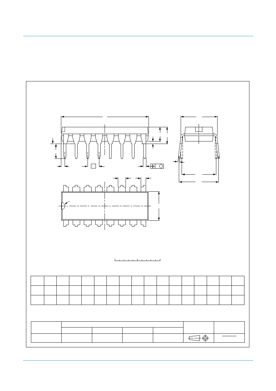
12. Package outline
Fig 10. SOT162-1.
UNIT
A
max.
A
1
A
2
A
3
b
p
c
D
(1)
E
(1)
(1)
e
H
E
L
L
p
Q
Z
y
w
v
REFERENCES
OUTLINE
VERSION
EUROPEAN
PROJECTION
ISSUE DATE
IEC
JEDEC
EIAJ
mm
inches
2.65
0.30
0.10
2.45
2.25
0.49
0.36
0.32
0.23
10.5
10.1
7.6
7.4
1.27
10.65
10.00
1.1
1.0
0.9
0.4
8
0
o
o
0.25
0.1
DIMENSIONS (inch dimensions are derived from the original mm dimensions)
Note
1. Plastic or metal protrusions of 0.15 mm maximum per side are not included.
1.1
0.4
SOT162-1
8
16
w
M
b
p
D
detail X
Z
e
9
1
y
0.25
075E03
MS-013
pin 1 index
0.10
0.012
0.004
0.096
0.089
0.019
0.014
0.013
0.009
0.41
0.40
0.30
0.29
0.050
1.4
0.055
0.419
0.394
0.043
0.039
0.035
0.016
0.01
0.25
0.01
0.004
0.043
0.016
0.01
X
A
A
1
A
2
H
E
L
p
Q
E
c
L
v
M
A
(A )
3
A
0
5
10 mm
scale
SO16: plastic small outline package; 16 leads; body width 7.5 mm
SOT162-1
97-05-22
99-12-27
Philips Semiconductors
SA572
Programmable analog compandor
Product data
Rev. 03 -- 3 November 1998
16 of 22
9397 750 07761
� Philips Electronics N.V. 2001. All rights reserved.
Fig 11. SOT38-4.
REFERENCES
OUTLINE
VERSION
EUROPEAN
PROJECTION
ISSUE DATE
IEC
JEDEC
EIAJ
SOT38-4
92-11-17
95-01-14
M
H
c
(e )
1
M
E
A
L
seating plane
A
1
w
M
b
1
b
2
e
D
A
2
Z
16
1
9
8
E
pin 1 index
b
0
5
10 mm
scale
Note
1. Plastic or metal protrusions of 0.25 mm maximum per side are not included.
UNIT
A
max.
1
2
b
1
(1)
(1)
(1)
b
2
c
D
E
e
M
Z
H
L
mm
DIMENSIONS (inch dimensions are derived from the original mm dimensions)
A
min.
A
max.
b
max.
w
M
E
e
1
1.73
1.30
0.53
0.38
0.36
0.23
19.50
18.55
6.48
6.20
3.60
3.05
0.254
2.54
7.62
8.25
7.80
10.0
8.3
0.76
4.2
0.51
3.2
inches
0.068
0.051
0.021
0.015
0.014
0.009
1.25
0.85
0.049
0.033
0.77
0.73
0.26
0.24
0.14
0.12
0.01
0.10
0.30
0.32
0.31
0.39
0.33
0.030
0.17
0.020
0.13
DIP16: plastic dual in-line package; 16 leads (300 mil)
SOT38-4

Philips Semiconductors
SA572
Programmable analog compandor
Product data
Rev. 03 -- 3 November 1998
17 of 22
9397 750 07761
� Philips Electronics N.V. 2001. All rights reserved.
13. Soldering
13.1 Introduction
This text gives a very brief insight to a complex technology. A more in-depth account
of soldering ICs can be found in our
Data Handbook IC26; Integrated Circuit
Packages (document order number 9398 652 90011).
There is no soldering method that is ideal for all IC packages. Wave soldering is often
preferred when through-hole and surface mount components are mixed on one
printed-circuit board. Wave soldering can still be used for certain surface mount ICs,
but it is not suitable for fine pitch SMDs. In these situations reflow soldering is
recommended.
13.2 Surface mount packages
13.2.1
Reflow soldering
Reflow soldering requires solder paste (a suspension of fine solder particles, flux and
binding agent) to be applied to the printed-circuit board by screen printing, stencilling
or pressure-syringe dispensing before package placement.
Several methods exist for reflowing; for example, convection or convection/infrared
heating in a conveyor type oven. Throughput times (preheating, soldering and
cooling) vary between 100 and 200 seconds depending on heating method.
Typical reflow peak temperatures range from 215 to 250
�
C. The top-surface
temperature of the packages should preferable be kept below 220
�
C for thick/large
packages, and below 235
�
C for small/thin packages.
13.2.2
Wave soldering
Conventional single wave soldering is not recommended for surface mount devices
(SMDs) or printed-circuit boards with a high component density, as solder bridging
and non-wetting can present major problems.
To overcome these problems the double-wave soldering method was specifically
developed.
If wave soldering is used the following conditions must be observed for optimal
results:
�
Use a double-wave soldering method comprising a turbulent wave with high
upward pressure followed by a smooth laminar wave.
�
For packages with leads on two sides and a pitch (e):
� larger than or equal to 1.27 mm, the footprint longitudinal axis is preferred to be
parallel to the transport direction of the printed-circuit board;
� smaller than 1.27 mm, the footprint longitudinal axis must be parallel to the
transport direction of the printed-circuit board.
The footprint must incorporate solder thieves at the downstream end.

Philips Semiconductors
SA572
Programmable analog compandor
Product data
Rev. 03 -- 3 November 1998
18 of 22
9397 750 07761
� Philips Electronics N.V. 2001. All rights reserved.
�
For packages with leads on four sides, the footprint must be placed at a 45
�
angle
to the transport direction of the printed-circuit board. The footprint must
incorporate solder thieves downstream and at the side corners.
During placement and before soldering, the package must be fixed with a droplet of
adhesive. The adhesive can be applied by screen printing, pin transfer or syringe
dispensing. The package can be soldered after the adhesive is cured.
Typical dwell time is 4 seconds at 250
�
C. A mildly-activated flux will eliminate the
need for removal of corrosive residues in most applications.
13.2.3
Manual soldering
Fix the component by first soldering two diagonally-opposite end leads. Use a low
voltage (24 V or less) soldering iron applied to the flat part of the lead. Contact time
must be limited to 10 seconds at up to 300
�
C.
When using a dedicated tool, all other leads can be soldered in one operation within
2 to 5 seconds between 270 and 320
�
C.
13.3 Through-hole mount packages
13.3.1
Soldering by dipping or by solder wave
The maximum permissible temperature of the solder is 260
�
C; solder at this
temperature must not be in contact with the joints for more than 5 seconds. The total
contact time of successive solder waves must not exceed 5 seconds.
The device may be mounted up to the seating plane, but the temperature of the
plastic body must not exceed the specified maximum storage temperature (T
stg(max)
).
If the printed-circuit board has been pre-heated, forced cooling may be necessary
immediately after soldering to keep the temperature within the permissible limit.
13.3.2
Manual soldering
Apply the soldering iron (24 V or less) to the lead(s) of the package, either below the
seating plane or not more than 2 mm above it. If the temperature of the soldering iron
bit is less than 300
�
C it may remain in contact for up to 10 seconds. If the bit
temperature is between 300 and 400
�
C, contact may be up to 5 seconds.

Philips Semiconductors
SA572
Programmable analog compandor
Product data
Rev. 03 -- 3 November 1998
19 of 22
9397 750 07761
� Philips Electronics N.V. 2001. All rights reserved.
13.4 Package related soldering information
[1]
All surface mount (SMD) packages are moisture sensitive. Depending upon the moisture content, the
maximum temperature (with respect to time) and body size of the package, there is a risk that internal
or external package cracks may occur due to vaporization of the moisture in them (the so called
popcorn effect). For details, refer to the Drypack information in the
Data Handbook IC26; Integrated
Circuit Packages; Section: Packing Methods.
[2]
For SDIP packages, the longitudinal axis must be parallel to the transport direction of the
printed-circuit board.
[3]
These packages are not suitable for wave soldering as a solder joint between the printed-circuit board
and heatsink (at bottom version) can not be achieved, and as solder may stick to the heatsink (on top
version).
[4]
If wave soldering is considered, then the package must be placed at a 45
�
angle to the solder wave
direction. The package footprint must incorporate solder thieves downstream and at the side corners.
[5]
Wave soldering is only suitable for LQFP, QFP and TQFP packages with a pitch (e) equal to or larger
than 0.8 mm; it is definitely not suitable for packages with a pitch (e) equal to or smaller than 0.65 mm.
[6]
Wave soldering is only suitable for SSOP and TSSOP packages with a pitch (e) equal to or larger than
0.65 mm; it is definitely not suitable for packages with a pitch (e) equal to or smaller than 0.5 mm.
14. Revision history
Table 5:
Suitability of IC packages for wave, reflow and dipping soldering methods
Mounting
Package
Soldering method
Wave
Reflow
[1]
Dipping
Through-hole
mount
DBS, DIP, HDIP, SDIP, SIL suitable
[2]
-
suitable
Surface mount
BGA, HBGA, LFBGA,
SQFP, TFBGA
not suitable
suitable
-
HBCC, HLQFP, HSQFP,
HSOP, HTQFP, HTSSOP,
HVQFN, SMS
not suitable
[3]
suitable
-
PLCC
[4]
, SO, SOJ
suitable
suitable
-
LQFP, QFP, TQFP
not recommended
[4] [5]
suitable
-
SSOP, TSSOP, VSO
not recommended
[6]
suitable
-
Table 6:
Revision history
Rev Date
CPCN
Description
03
19981103
853-0813 20294
Product specification; third version; supersedes second version SA572_2
of 1998 Nov 03 (9397 750 04749). Modifications:
The format of this specification has been redesigned to comply with Philips
Semiconductors' new presentation and information standard.
02
19981103
853-0813 20294
Product specification; second version; supersedes first version SA572_1
of 1987 Oct 07. Modifications:
Changed prefix from NE to SA.
01
19871007
853-0813 90829
Product specification; initial version.

Philips Semiconductors
SA572
Programmable analog compandor
Product data
Rev. 03 -- 3 November 1998
20 of 22
9397 750 07761
� Philips Electronics N.V. 2001 All rights reserved.
15. Data sheet status
[1]
Please consult the most recently issued data sheet before initiating or completing a design.
[2]
The product status of the device(s) described in this data sheet may have changed since this data sheet was published. The latest information is available on the Internet at
URL http://www.semiconductors.philips.com.
16. Definitions
Short-form specification -- The data in a short-form specification is
extracted from a full data sheet with the same type number and title. For
detailed information see the relevant data sheet or data handbook.
Limiting values definition -- Limiting values given are in accordance with
the Absolute Maximum Rating System (IEC 60134). Stress above one or
more of the limiting values may cause permanent damage to the device.
These are stress ratings only and operation of the device at these or at any
other conditions above those given in the Characteristics sections of the
specification is not implied. Exposure to limiting values for extended periods
may affect device reliability.
Application information -- Applications that are described herein for any
of these products are for illustrative purposes only. Philips Semiconductors
make no representation or warranty that such applications will be suitable for
the specified use without further testing or modification.
17. Disclaimers
Life support -- These products are not designed for use in life support
appliances, devices, or systems where malfunction of these products can
reasonably be expected to result in personal injury. Philips Semiconductors
customers using or selling these products for use in such applications do so
at their own risk and agree to fully indemnify Philips Semiconductors for any
damages resulting from such application.
Right to make changes -- Philips Semiconductors reserves the right to
make changes, without notice, in the products, including circuits, standard
cells, and/or software, described or contained herein in order to improve
design
and/or
performance.
Philips
Semiconductors
assumes
no
responsibility or liability for the use of any of these products, conveys no
licence or title under any patent, copyright, or mask work right to these
products, and makes no representations or warranties that these products
are free from patent, copyright, or mask work right infringement, unless
otherwise specified.
Data sheet status
[1]
Product status
[2]
Definition
Objective data
Development
This data sheet contains data from the objective specification for product development. Philips Semiconductors
reserves the right to change the specification in any manner without notice.
Preliminary data
Qualification
This data sheet contains data from the preliminary specification. Supplementary data will be published at a
later date. Philips Semiconductors reserves the right to change the specification without notice, in order to
improve the design and supply the best possible product.
Product data
Production
This data sheet contains data from the product specification. Philips Semiconductors reserves the right to
make changes at any time in order to improve the design, manufacturing and supply. Changes will be
communicated according to the Customer Product/Process Change Notification (CPCN) procedure
SNW-SQ-650A.

Philips Semiconductors
SA572
Programmable analog compandor
Product data
Rev. 03 -- 3 November 1998
21 of 22
9397 750 07761
� Philips Electronics N.V. 2001. All rights reserved.
Philips Semiconductors - a worldwide company
Argentina:
see South America
Australia:
Tel. +61 2 9704 8141, Fax. +61 2 9704 8139
Austria:
Tel. +43 160 101, Fax. +43 160 101 1210
Belarus:
Tel. +375 17 220 0733, Fax. +375 17 220 0773
Belgium:
see The Netherlands
Brazil:
see South America
Bulgaria:
Tel. +359 268 9211, Fax. +359 268 9102
Canada:
Tel. +1 800 234 7381
China/Hong Kong:
Tel. +852 2 319 7888, Fax. +852 2 319 7700
Colombia:
see South America
Czech Republic:
see Austria
Denmark:
Tel. +45 3 288 2636, Fax. +45 3 157 0044
Finland:
Tel. +358 961 5800, Fax. +358 96 158 0920
France:
Tel. +33 1 4728 6600, Fax. +33 1 4728 6638
Germany:
Tel. +49 40 23 5360, Fax. +49 402 353 6300
Hungary:
Tel. +36 1 382 1700, Fax. +36 1 382 1800
India:
Tel. +91 22 493 8541, Fax. +91 22 493 8722
Indonesia:
see Singapore
Ireland:
Tel. +353 17 64 0000, Fax. +353 17 64 0200
Israel:
Tel. +972 36 45 0444, Fax. +972 36 49 1007
Italy:
Tel. +39 039 203 6838, Fax +39 039 203 6800
Japan:
Tel. +81 33 740 5130, Fax. +81 3 3740 5057
Korea:
Tel. +82 27 09 1412, Fax. +82 27 09 1415
Malaysia:
Tel. +60 37 50 5214, Fax. +60 37 57 4880
Mexico:
Tel. +9-5 800 234 7381
Middle East:
see Italy
Netherlands:
Tel. +31 40 278 2785, Fax. +31 40 278 8399
New Zealand:
Tel. +64 98 49 4160, Fax. +64 98 49 7811
Norway:
Tel. +47 22 74 8000, Fax. +47 22 74 8341
Philippines:
Tel. +63 28 16 6380, Fax. +63 28 17 3474
Poland:
Tel. +48 22 5710 000, Fax. +48 22 5710 001
Portugal:
see Spain
Romania:
see Italy
Russia:
Tel. +7 095 755 6918, Fax. +7 095 755 6919
Singapore:
Tel. +65 350 2538, Fax. +65 251 6500
Slovakia:
see Austria
Slovenia:
see Italy
South Africa:
Tel. +27 11 471 5401, Fax. +27 11 471 5398
South America:
Tel. +55 11 821 2333, Fax. +55 11 829 1849
Spain:
Tel. +34 33 01 6312, Fax. +34 33 01 4107
Sweden:
Tel. +46 86 32 2000, Fax. +46 86 32 2745
Switzerland:
Tel. +41 14 88 2686, Fax. +41 14 81 7730
Taiwan:
Tel. +886 22 134 2451, Fax. +886 22 134 2874
Thailand:
Tel. +66 23 61 7910, Fax. +66 23 98 3447
Turkey:
Tel. +90 216 522 1500, Fax. +90 216 522 1813
Ukraine:
Tel. +380 44 264 2776, Fax. +380 44 268 0461
United Kingdom:
Tel. +44 208 730 5000, Fax. +44 208 754 8421
United States:
Tel. +1 800 234 7381
Uruguay:
see South America
Vietnam:
see Singapore
Yugoslavia:
Tel. +381 11 3341 299, Fax. +381 11 3342 553
For all other countries apply to: Philips Semiconductors,
Marketing Communications,
Building BE, P.O. Box 218, 5600 MD EINDHOVEN,
The Netherlands, Fax. +31 40 272 4825
Internet: http://www.semiconductors.philips.com
(SCA72)

� Philips Electronics N.V. 2001.
Printed in the U.S.A
All rights are reserved. Reproduction in whole or in part is prohibited without the prior
written consent of the copyright owner.
The information presented in this document does not form part of any quotation or
contract, is believed to be accurate and reliable and may be changed without notice. No
liability will be accepted by the publisher for any consequence of its use. Publication
thereof does not convey nor imply any license under patent- or other industrial or
intellectual property rights.
Date of release: 3 November 1998
Document order number: 9397 750 07761
Contents
Philips Semiconductors
SA572
Programmable analog compandor
1
Description . . . . . . . . . . . . . . . . . . . . . . . . . . . . . 1
2
Features . . . . . . . . . . . . . . . . . . . . . . . . . . . . . . . 1
3
Applications . . . . . . . . . . . . . . . . . . . . . . . . . . . . 1
4
Ordering information . . . . . . . . . . . . . . . . . . . . . 2
5
Block diagram . . . . . . . . . . . . . . . . . . . . . . . . . . 2
6
Pinning information . . . . . . . . . . . . . . . . . . . . . . 3
6.1
Pinning . . . . . . . . . . . . . . . . . . . . . . . . . . . . . . . 3
6.2
Pin description . . . . . . . . . . . . . . . . . . . . . . . . . 3
7
Functional description . . . . . . . . . . . . . . . . . . . 4
7.1
Audio signal processing IC combines VCA
and fast attack/slow recovery level sensor . . . 4
8
Limiting values. . . . . . . . . . . . . . . . . . . . . . . . . . 4
9
Static characteristics. . . . . . . . . . . . . . . . . . . . . 5
10
Test circuit . . . . . . . . . . . . . . . . . . . . . . . . . . . . . 6
11
Application information. . . . . . . . . . . . . . . . . . . 6
11.1
SA572 Basic applications . . . . . . . . . . . . . . . . . 6
11.1.1
Description . . . . . . . . . . . . . . . . . . . . . . . . . . . . 6
11.1.2
Gain cell . . . . . . . . . . . . . . . . . . . . . . . . . . . . . . 7
11.1.3
Rectifier. . . . . . . . . . . . . . . . . . . . . . . . . . . . . . . 8
11.1.4
Buffer amplifier . . . . . . . . . . . . . . . . . . . . . . . . . 9
11.1.5
Basic expandor . . . . . . . . . . . . . . . . . . . . . . . . 11
11.1.6
Basic compressor . . . . . . . . . . . . . . . . . . . . . . 12
11.1.7
Basic compandor system . . . . . . . . . . . . . . . . 13
12
Package outline . . . . . . . . . . . . . . . . . . . . . . . . 15
13
Soldering . . . . . . . . . . . . . . . . . . . . . . . . . . . . . 17
13.1
Introduction . . . . . . . . . . . . . . . . . . . . . . . . . . 17
13.2
Surface mount packages . . . . . . . . . . . . . . . . 17
13.2.1
Reflow soldering . . . . . . . . . . . . . . . . . . . . . . . 17
13.2.2
Wave soldering . . . . . . . . . . . . . . . . . . . . . . . . 17
13.2.3
Manual soldering . . . . . . . . . . . . . . . . . . . . . . 18
13.3
Through-hole mount packages . . . . . . . . . . . . 18
13.3.1
Soldering by dipping or by solder wave . . . . . 18
13.3.2
Manual soldering . . . . . . . . . . . . . . . . . . . . . . 18
13.4
Package related soldering information . . . . . . 19
14
Revision history . . . . . . . . . . . . . . . . . . . . . . . . 19
15
Data sheet status . . . . . . . . . . . . . . . . . . . . . . . 20
16
Definitions . . . . . . . . . . . . . . . . . . . . . . . . . . . . 20
17
Disclaimers. . . . . . . . . . . . . . . . . . . . . . . . . . . . 20