 | –≠–ª–µ–∫—Ç—Ä–æ–Ω–Ω—ã–π –∫–æ–º–ø–æ–Ω–µ–Ω—Ç: SA606N | –°–∫–∞—á–∞—Ç—å:  PDF PDF  ZIP ZIP |
Document Outline
- DESCRIPTION
- FEATURES
- PIN CONFIGURATION
- APPLICATIONS
- ORDERING INFORMATION
- ABSOLUTE MAXIMUM RATINGS
- BLOCK DIAGRAM
- DC ELECTRICAL CHARACTERISTICS
- AC ELECTRICAL CHARACTERISTICS
- CIRCUIT DESCRIPTION
- PACKAGING
- DEFINITIONS
Philips Semiconductors
SA606
Low-voltage high performance mixer FM
IF system
Product Specification
Replaces data of October 26, 1993
1997 Nov 07
RF COMMUNICATIONS PRODUCTS
20
19
18
17
16
15
14
13
12
11
10
9
8
7
6
5
4
3
2
1
RSSI
IF
AMP
E
B
VREG
OSCILLATOR
LIMITER
MIXER
QUAD
+
≠
+
≠
AUDIO
RF Data Handbook

Philips Semiconductors
Product specification
SA606
Low-voltage high performance mixer FM IF system
2
1997 Nov 07
853-1576 18665
DESCRIPTION
The SA606 is a low-voltage high performance monolithic FM IF
system incorporating a mixer/oscillator, two limiting intermediate
frequency amplifiers, quadrature detector, logarithmic received
signal strength indicator (RSSI), voltage regulator and audio and
RSSI op amps. The SA606 is available in 20-lead SOL
(surface-mounted small outline large package) and 20-lead SSOP
(shrink small outline package).
The SA606 was designed for portable communication applications
and will function down to 2.7V. The RF section is similar to the
famous SA605. The audio and RSSI outputs have amplifiers with
access to the feedback path. This enables the designer to level
adjust the outputs or add filtering.
FEATURES
∑
Low power consumption: 3.5mA typical at 3V
∑
Mixer input to >150MHz
∑
Mixer conversion power gain of 17dB at 45MHz
∑
XTAL oscillator effective to 150MHz (L.C. oscillator or external
oscillator can be used at higher frequencies)
∑
102dB of IF Amp/Limiter gain
∑
2MHz limiter small signal bandwidth
∑
Temperature compensated logarithmic Received Signal Strength
Indicator (RSSI) with a 90dB dynamic range
∑
Low external component count; suitable for crystal/ceramic/LC
filters
∑
Excellent sensitivity: 0.31
µ
V into 50
matching network for 12dB
SINAD (Signal to Noise and Distortion ratio) for 1kHz tone with RF
at 45MHz and IF at 455kHz
∑
SA606 meets cellular radio specifications
∑
Audio output internal op amp
∑
RSSI output internal op amp
∑
Internal op amps with rail-to-rail outputs
PIN CONFIGURATION
RF IN+
RF IN- DECOUPLING
OSCOUT
OSCIN
RSSI
MIXER OUT
IF AMP IN
IF AMP OUT
GND
LIMITER IN
LIMITER OUT
VCC
D and DK Packages
AUDIO FEEDBACK
RSSI FEEDBACK
QUADRATURE IN
IF AMP DECOUPLING
AUDIO
IF AMP DECOUPLING
LIMITER DECOUPLING
LIMITER DECOUPLING
1
2
3
4
5
6
7
8
9
10
20
19
18
17
16
15
14
13
12
11
SR00347
Figure 1. Pin Configuration
∑
ESD protection: Human Body Model 2kV
Robot Model 200V
APPLICATIONS
∑
Portable cellular radio FM IF
∑
Cordless phones
∑
Wireless systems
∑
RF level meter
∑
Spectrum analyzer
∑
Instrumentation
∑
FSK and ASK data receivers
∑
Log amps
∑
Portable high performance communication receiver
∑
Single conversion VHF receivers
ORDERING INFORMATION
DESCRIPTION
TEMPERATURE RANGE
ORDER CODE
DWG #
20-Pin Plastic Small Outline Large (SOL) package (Surface-mount)
-40 to +85
∞
C
SA606D
SOT163-1
20-Pin Plastic Shrink Small Outline Package (SSOP) (Surface-mount)
-40 to +85
∞
C
SA606DK
SOT266-1
ABSOLUTE MAXIMUM RATINGS
SYMBOL
PARAMETER
RATING
UNITS
V
CC
Single supply voltage
7
V
T
STG
Storage temperature range
-65 to +150
∞
C
T
A
Operating ambient temperature range
-40 to +85
∞
C
JA
Thermal impedance
D package
DK package
90
117
∞
C/W
Philips Semiconductors
Product specification
SA606
Low-voltage high performance mixer FM IF system
1997 Nov 07
3
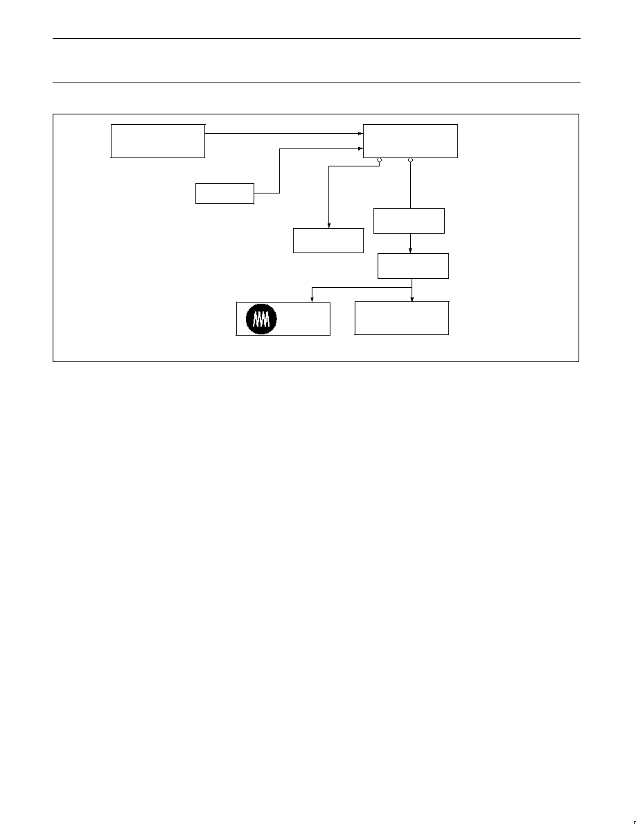
BLOCK DIAGRAM
20
19
18
17
16
15
14
13
12
11
10
9
8
7
6
5
4
3
2
1
RSSI
IF
AMP
E
B
VREG
OSCILLATOR
LIMITER
MIXER
QUAD
+ ≠
+
≠
AUDIO
SR00348
Figure 2. Block Diagram
DC ELECTRICAL CHARACTERISTICS
V
CC
= +3V, T
A
= 25
∞
C; unless otherwise stated.
SYMBOL
PARAMETER
TEST CONDITIONS
LIMITS
UNITS
SYMBOL
PARAMETER
TEST CONDITIONS
MIN
TYP
MAX
UNITS
V
CC
Power supply voltage range
2.7
7.0
V
I
CC
DC current drain
3.5
4.2
mA
AC ELECTRICAL CHARACTERISTICS
T
A
= 25
∞
C; V
CC
= +3V, unless otherwise stated. RF frequency = 45MHz + 14.5dBV RF input step-up; IF frequency = 455kHz; R17 = 2.4k
and R18 = 3.3k
; RF level = -45dBm; FM modulation = 1kHz with
±
8kHz peak deviation. Audio output with de-emphasis filter and C-message
weighted filter. Test circuit Figure 3. The parameters listed below are tested using automatic test equipment to assure consistent electrical
characterristics. The limits do not represent the ultimate performance limits of the device. Use of an optimized RF layout will improve many of
the listed parameters.
SYMBOL
PARAMETER
TEST CONDITIONS
LIMITS
UNITS
SYMBOL
PARAMETER
TEST CONDITIONS
MIN
TYP
MAX
UNITS
Mixer/Osc section (ext LO = 220mV
RMS
)
f
IN
Input signal frequency
150
MHz
f
OSC
Crystal oscillator frequency
150
MHz
Noise figure at 45MHz
6.2
dB
Third-order input intercept point (50
source)
f1 = 45.0; f2 = 45.06MHz
Input RF level = -52dBm
-9
dBm
Conversion voltage gain
Matched 14.5dBV step-up
13.5
17
19.5
dB
50
source
+2.5
dB
RF input resistance
Single-ended input
8
k
RF input capacitance
3.0
4.0
pF
Mixer output resistance
(Pin 20)
1.25
1.5
k
IF section
IF amp gain
50
source
44
dB
Limiter gain
50
source
58
dB
Input limiting -3dB, R
17a
= 2.4k, R
17b
= 3.3k
Test at Pin 18
-109
dBm
AM rejection
80% AM 1kHz
45
dB
Audio level
Gain of two (2k
AC load)
70
120
160
mV
SINAD sensitivity
IF level -110dBm
17
dB

Philips Semiconductors
Product specification
SA606
Low-voltage high performance mixer FM IF system
1997 Nov 07
4
AC ELECTRICAL CHARACTERISTICS
(Continued)
SYMBOL
PARAMETER
TEST CONDITIONS
LIMITS
UNITS
SYMBOL
PARAMETER
TEST CONDITIONS
MIN
TYP
MAX
UNITS
THD
Total harmonic distortion
-35
-50
dB
S/N
Signal-to-noise ratio
No modulation for noise
62
dB
RF RSSI output, R
9
= 2k
RF level = -118dBm
0.3
.80
V
RF level = -68dBm
.70
1.1
1.80
V
RF level = -23dBm
1.20
1.8
2.50
V
RSSI range
90
dB
RSSI accuracy
+1.5
dB
IF input impedance
Pin 18
1.3
1.5
k
IF output impedance
Pin 16
0.3
k
Limiter input impedance
Pin 14
1.3
1.5
k
Limiter output impedance
Pin 11
0.3
k
Limiter output voltage
Pin 11
130
mV
RMS
RF/IF section (int LO)
Audio level
3V = V
CC
, RF level = -27dBm
120
mV
RMS
System RSSI output
3V = V
CC
, RF level = -27dBm
2.2
V
System SINAD sensitivity
RF level = -117dBm
12
dB
CIRCUIT DESCRIPTION
The SA606 is an IF signal processing system suitable for second IF
systems with input frequency as high as 150MHz. The bandwidth of
the IF amplifier and limiter is at least 2MHz with 90dB of gain. The
gain/bandwidth distribution is optimized for 455kHz, 1.5k
source
applications. The overall system is well-suited to battery operation
as well as high performance and high quality products of all types.
The input stage is a Gilbert cell mixer with oscillator. Typical mixer
characteristics include a noise figure of 6.2dB, conversion gain of
17dB, and input third-order intercept of -9dBm. The oscillator will
operate in excess of 200MHz in L/C tank configurations. Hartley or
Colpitts circuits can be used up to 100MHz for xtal configurations.
Butler oscillators are recommended for xtal configurations up to
150MHz.
The output impedance of the mixer is a 1.5k
resistor permitting
direct connection to a 455kHz ceramic filter. The input resistance of
the limiting IF amplifiers is also 1.5k
. With most 455kHz ceramic
filters and many crystal filters, no impedance matching network is
necessary. The IF amplifier has 43dB of gain and 5.5MHz
bandwidth. The IF limiter has 60dB of gain and 4.5MHz bandwidth.
To achieve optimum linearity of the log signal strength indicator,
there must be a 12dB(v) insertion loss between the first and second
IF stages. If the IF filter or interstage network does not cause
12dB(v) insertion loss, a fixed or variable resistor or an L pad for
simultaneous loss and impedance matching can be added between
the first IF output (Pin 16) and the interstage network. The overall
gain will then be 90dB with 2MHz bandwidth.
The signal from the second limiting amplifier goes to a Gilbert cell
quadrature detector. One port of the Gilbert cell is internally driven
by the IF. The other output of the IF is AC-coupled to a tuned
quadrature network. This signal, which now has a 90
∞
phase
relationship to the internal signal, drives the other port of the
multiplier cell.
The demodulated output of the quadrature drives an internal op
amp. This op amp can be configured as a unity gain buffer, or for
simultaneous gain, filtering, and 2nd-order temperature
compensation if needed. It can drive an AC load as low as 5k
with
a rail-to-rail output.
A log signal strength completes the circuitry. The output range is
greater than 90dB and is temperature compensated. This log signal
strength indicator exceeds the criteria for AMPs or TACs cellular
telephone. This signal drives an internal op amp. The op amp is
capable of rail-to-rail output. It can be used for gain, filtering, or
2nd-order temperature compensation of the RSSI, if needed.
NOTE: dB(v) = 20log V
OUT
/V
IN
Philips Semiconductors
Product specification
SA606
Low-voltage high performance mixer FM IF system
1997 Nov 07
5
10
9
8
7
6
5
4
3
2
1
20
19
18
17
16
15
14
13
12
11
RSSI
IF
AMP
MIXER
QUAD
MINI≠CIRCUIT ZSC2≠1B
AUDIO
C14
IFT1
C10
C9
C8
C7
C6
X1
R7
30.5
L2
SW3
SW4
SW1
VCC
EXT.
LOC
OSC
44.545
45MHZ
R3
R1
R2
SW2
C3
C4
R4
51.1
C5
C2
C1
L1
R6
178
R8
39.2
"C" WEIGHTED
AUDIO
MEASUREMENT
CIRCUIT
45.06
MHZ
50.5
2430
3880
96.5
32.6
71.5
C24
C22
C20
C19
C18
C15
C16
C17
FLT2
SW7
SW6
SW5
SW8
SW9
C23
C21
R17
2.4k
FLT1
-
25dB,
1500/50
PAD
-
10dB,
50/50
PAD
-
29dB,
929/50
PAD
-
10.6dB,
50/50
PAD
-
36dB,
156k/50
PAD
100pF NPO Ceramic
390pF NPO Ceramic
22pF NPO Ceramic
1nF Ceramic
10.0pF NPO Ceramic
10pF NPO Ceramic
100nF +10% Monolithic Ceramic
100nF +10% Monolithic Ceramic
100nF +10% Monolithic Ceramic
100nF +10% Monolithic Ceramic
2.2
µ
F
100nF +10% Monolithic Ceramic
10
µ
F Tantalum (minimum) *
C21
C23
C27
Flt 1
Flt 2
IFT 1
L1
L2
X1
R9
R17
R10
R11
100nF +10% Monolithic Ceramic
100nF +10% Monolithic Ceramic
10k
+1%
10k
+1%
2.4k
+5% 1/4W Carbon Composition
2k
+1% 1/4W Metal Film
44.545MHz Crystal ICM4712701
0.8
µ
H nominal
Toko 292CNS≠T1038Z
455kHz (Ce = 180pF) Toko RMC≠2A6597H
Ceramic Filter Murata SFG455A3 or equiv
Ceramic Filter Murata SFG455A3 or equiv
2.2
µ
F +10% Monolithic Ceramic
147≠160nH Coilcraft UNI≠10/142≠04J08S
C1
C2
C5
C6
C7
C8
C9
C10
C12
C14
C15
C17
C18
Automatic Test Circuit Component List
1.3k
51.7
71.5
96.5
32.8
51.5
OSCILLATOR
R12
2k
+1%
R13
20k
+1%
R14
10k
+1%
R9
R12
DEEMPHASIS
FILTER
LIMITER
VREG
SW10
SW11
R11
R13
R10
+ ≠
+
≠
C12
AUDIO
R14
RSSI
16k
R19
C25
100nF +10% Monolithic Ceramic
R18
R19
16k
R18
3.3k
3.3k
C26
C26
100nF +10% Monolithic Ceramic
C27
*NOTE: This value can be reduced when a battery is the power source.
SR00349
Figure 3. SA606 45MHz Test Circuit (Relays as shown)
Philips Semiconductors
Product specification
SA606
Low-voltage high performance mixer FM IF system
1997 Nov 07
6
10
8
7
6
4
3
2
1
5
9
20
19
18
17
16
14
13
12
11
15
RSSI
IF
AMP
MIXER
QUAD
RSSI
OUTPUT
AUDIO
C14
IFT1
C10
C9
C8
C7
C6
X1
L2
VCC
C5
C2
C1
L1
C18
C15
C17
FLT2
C23
C21
R17
2.4k
FLT1
51pF NPO Ceramic
220pF NPO Ceramic
5-30pF trim cap
1nF Ceramic
10.0pF NPO Ceramic
10pF NPO Ceramic
100nF +10% Monolithic Ceramic
100nF +10% Monolithic Ceramic
100nF +10% Monolithic Ceramic
100nF +10% Monolithic Ceramic
2.2
µ
F +10% Tantalum
100nF +10% Monolithic Ceramic
10
µ
F Tantalum (minimum) *
C26
C27
Flt 1
Flt 2
IFT 1
L1
L2
X1
R10
R5
100nF +10% Monolithic Ceramic
2.2
µ
F Tantalum
Not Used in Application Board (see Note 8, pg 8)
8.2k +5% 1/4W Carbon Composition
44.545MHz Crystal ICM4712701
1.2
µ
H
Ceramic Filter Murata SFG455A3 or equiv
Ceramic Filter Murata SFG455A3 or equiv
C1
C2
C5
C6
C7
C8
C9
C10
C12
C14
C15
C17
C18
Application Component List
45MHz
INPUT
LIMITER
VREG
OSCILLATOR
+ ≠
+
≠
C12
C26
R18
3.3k
R19
11k
C27
R10
R11
10k
10k
C19
C23
390pF +10% Monolithic Ceramic
100nF +10% Monolithic Ceramic
R11
10k +5% 1/4W Carbon Composition
R17
R18
2.4k +5% 1/4W Carbon Composition
3.3k +5% 1/4W Carbon Composition
R19
11k +5% 1/4W Carbon Composition
NE606D/DK Demo Board
C19
390pF
.33
µ
H TOKO SCB-1320Z
330
µ
H TOKO 303LN-1130
C21
100nF +10% Monolithic Ceramic
2.2
µ
F
* NOTE: This value can be reduced when a battery is the power source.
SR00350
Figure 4. SA606 45MHz Application Circuit
Philips Semiconductors
Product specification
SA606
Low-voltage high performance mixer FM IF system
1997 Nov 07
7
RF GENERATOR
NE606 DEMO BOARD
C≠MESSAGE
HP339A DISTORTION
ANALYZER
SCOPE
DC VOLTMETER
V
CC
(+3)
45MHz
DE-EMPHASIS
FILTER
RSSI
AUDIO
SR00351
Figure 5. SA606 Application Circuit Test Set Up
NOTES:
1. C-message: The C-message and de-emphasis filter combination has a peak gain of 10 for accurate measurements. Without the gain, the
measurements may be affected by the noise of the scope and HP339 analyzer. The de-emphasis filter has a fixed -6dB/Octave slope
between 300Hz and 3kHz.
2. Ceramic filters: The ceramic filters can be 30kHz SFG455A3s made by Murata which have 30kHz IF bandwidth (they come in blue), or
16kHz CFU455Ds, also made by Murata (they come in black). All of our specifications and testing are done with the more wideband filter.
3. RF generator: Set your RF generator at 45.000MHz, use a 1kHz modulation frequency and a 6kHz deviation if you use 16kHz filters, or
8kHz if you use 30kHz filters.
4. Sensitivity: The measured typical sensitivity for 12dB SINAD should be 0.35
µ
V or -116dBm at the RF input.
5. Layout: The layout is very critical in the performance of the receiver. We highly recommend our demo board layout.
6. RSSI: The smallest RSSI voltage (i.e., when no RF input is present and the input is terminated) is a measure of the quality of the layout and
design. If the lowest RSSI voltage is 500mV or higher, it means the receiver is in regenerative mode. In that case, the receiver sensitivity
will be worse than expected.
7. Supply bypass and shielding: All of the inductors, the quad tank, and their shield must be grounded. A 10-15
µ
F or higher value tantalum
capacitor on the supply line is essential. A low frequency ESR screening test on this capacitor will ensure consistent good sensitivity in
production. A 0.1
µ
F bypass capacitor on the supply pin, and grounded near the 44.545MHz oscillator improves sensitivity by 2-3dB.
8. R5 can be used to bias the oscillator transistor at a higher current for operation above 45MHz. Recommended value is 10k
.
Philips Semiconductors
Product specification
SA606
Low-voltage high performance mixer FM IF system
1997 Nov 07
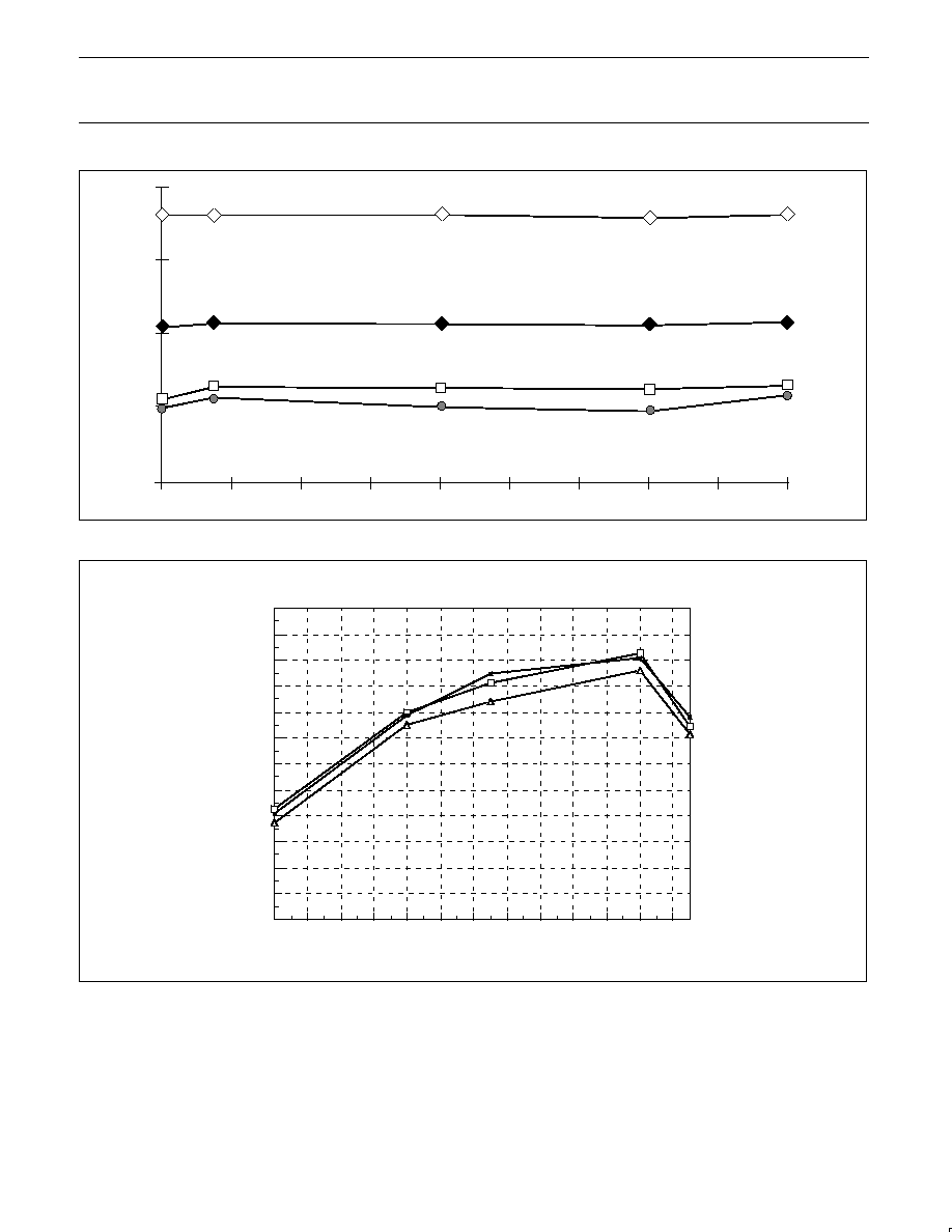
8
6
5
4
3
2
≠55
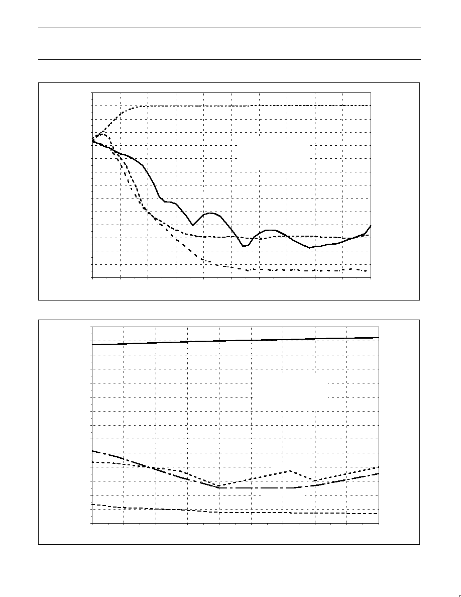
≠35
≠15
5
25
45
65
85
105
125
VCC = 2.7V
VCC = 3V
VCC = 5V
VCC = 7V
mA
∞
C
SR00352
Figure 6. I
CC
vs Temperature
Temperature (
∞
C)
50 INPUT INTERCEPT POINT (dBm)
≠8.0
≠8.5
≠9.0
≠9.5
≠10.0
≠10.5
≠11.0
≠11.5
≠12.0
≠12.5
≠13.0
≠13.5
≠14.0
≠40
≠30
≠20
≠10
0
10
20
30
40
50
60
70
80
7V
3V
2.7V
SR00353
Figure 7. Third Order Intercept Point vs Supply Voltage

Philips Semiconductors
Product specification
SA606
Low-voltage high performance mixer FM IF system
1997 Nov 07
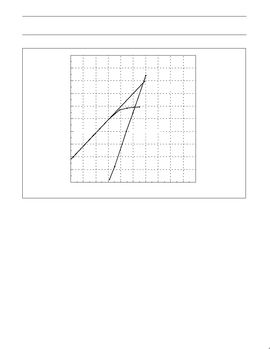
9
TEMPERATURE (
∞
C)
NOISE FIGURE
8.00
7.75
7.50
7.25
7.00
6.75
6.50
6.25
6.00
5.75
5.50
5.25
5.00
≠40
≠30
≠20
≠10
0
10
20
30
40
50
60
70
80
2.7V
3V
7.0V
SR00354
Figure 8. Mixer Noise Figure vs Supply Voltage
TEMPERATURE (
∞
C)
18.00
17.75
17.50
17.25
17.00
16.75
16.50
16.25
16.00
≠40
≠30
≠20
≠10
0
10
20
30
40
50
60
70
80
2.7V
3V
7.0V
CONVERSION GAIN (dB)
SR00355
Figure 9. Conversion Gain vs Supply Voltage
Philips Semiconductors
Product specification
SA606
Low-voltage high performance mixer FM IF system
1997 Nov 07
10
20
10
0
≠10
≠20
≠30
≠40
≠50
≠60
≠70
≠80
≠66
≠56
≠46
≠36
≠26
≠16
≠6
4
14
24
34
FUND PRODUCT
3rd ORDER PRODUCT
*50
INPUT
IF
OUTPUT
POWER (≠dBm)
RF* INPUT LEVEL (dBm)
RF = 45MHz
IF = 455kHz
SR00356
Figure 10. Mixer Third Order Intercept and Compression
Philips Semiconductors
Product specification
SA606
Low-voltage high performance mixer FM IF system
1997 Nov 07
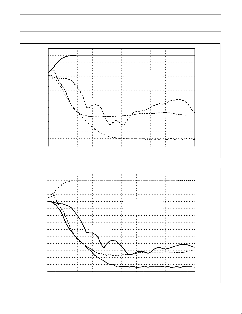
11
DECIBELS (dB)
5
≠125
≠115
≠105
≠95
≠85
≠75
≠65
≠55
≠45
≠35
≠25
RF LEVEL (dBm)
0
≠5
≠10
≠15
≠20
≠25
≠30
≠35
≠40
≠45
≠50
≠55
≠60
≠65
VCC = 3V
RF = 45MHz
DEVIATION =
±
8kHz
AUDIO LEVEL = 104.9mVRMS
AUDIO
THD + NOISE
AM REJECTION
NOISE
SR00357
Figure 11. Sensitivity vs RF Level (-40
∞
C)
DECIBELS (dB)
5
≠125
≠115
≠105
≠95
≠85
≠75
≠65
≠55
≠45
≠35
≠25
RF LEVEL (dBm)
0
≠5
≠10
≠20
≠25
≠30
≠35
≠40
≠45
≠50
≠55
≠60
≠65
VCC = 3V
RF = 45MHz
DEVIATION =
±
8kHz
AUDIO LEVEL = 117.6mVRMS
AUDIO
THD + NOISE
AM REJECTION
NOISE
SR00358
Figure 12. Sensitivity vs RF Level (+25
∞
C)
Philips Semiconductors
Product specification
SA606
Low-voltage high performance mixer FM IF system
1997 Nov 07
12
DECIBELS (dB)
5
≠125
≠115
≠105
≠95
≠85
≠75
≠65
≠55
≠45
≠35
≠25
RF LEVEL (dBm)
0
≠5
≠10
≠15
≠20
≠25
≠30
≠35
≠40
≠45
≠50
≠55
≠60
≠65
VCC = 3V
RF = 45MHz
DEVIATION =
±
8kHz
AUDIO LEVEL = 127mVRMS
AUDIO
THD + NOISE
AM REJECTION
NOISE
SR00359
Figure 13. Sensitivity vs RF Level (Temperature 85
∞
C)
DECIBELS (dB)
5
0
≠5
≠10
≠15
≠20
≠25
≠30
≠35
≠40
≠45
≠50
≠55
≠60
≠65
≠55
≠35
≠15
5
25
45
65
85
105
125
TEMPERATURE (
∞
C)
VCC = 3V
RF = 45MHz
DEVIATION =
±
8kHz
AUDIO LEVEL = +117.6mVRMS
AUDIO
DISTORTION
AM REJECTION
NOISE
RF LEVEL = -45dBm
SR00360
Figure 14. Relative Audio Level, Distortion, AM Rejection and Noise vs Temperature

Philips Semiconductors
Product specification
SA606
Low-voltage high performance mixer FM IF system
1997 Nov 07
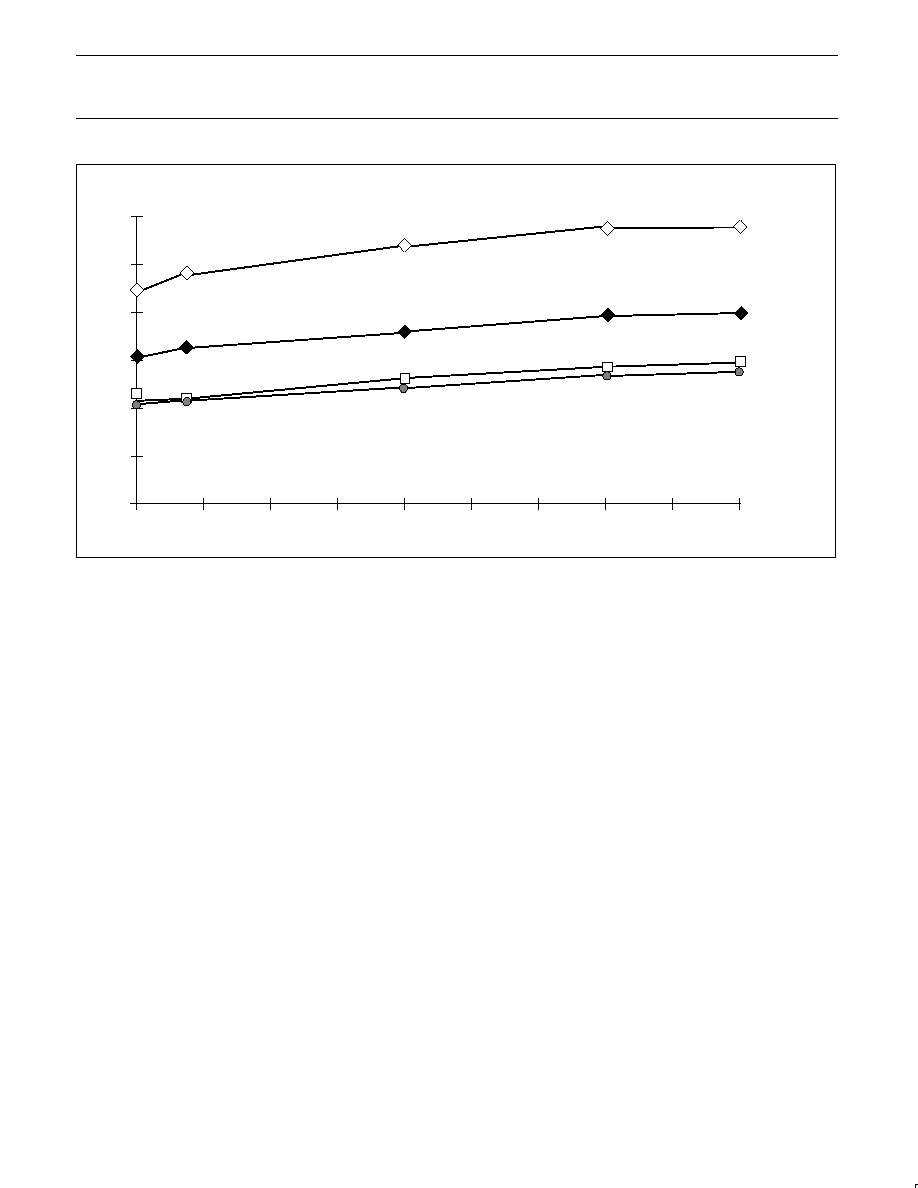
13
2.400
2.000
1.600
1.200
0.800
0.400
0.000
≠95
≠85
≠75
≠65
≠55
≠45
≠35
≠25
≠15
≠5
5
IF LEVEL (dBm)
+85
∞
C
-40
∞
C
ROOM
VOL
T
AGE (V)
SR00361
Figure 15. RSSI (455kHz IF @ 3V)
VOL
T
AGE (V)
2.1
2.0
1.9
1.8
1.7
1.6
1.5
1.4
1.3
1.2
1.1
1.0
0.9
0.8
0.7
0.6
0.5
0.4
0.3
≠125
≠115
≠105
≠95
≠85
≠75
≠65
≠55
≠45
≠35
≠25
RF LEVEL (dBm)
+85
∞
C
+27
∞
C
-40
∞
C
SR00362
Figure 16. RSSI vs RF Level and Temperature - V
CC
= 3V
Philips Semiconductors
Product specification
SA606
Low-voltage high performance mixer FM IF system
1997 Nov 07
14
300
≠55
≠35
≠15
5
25
45
65
85
105
125
VCC = 2.7V
VCC = 3V
VCC = 5V
VCC = 7V
250
200
150
100
50
0
mV
RMS
V
∞
C
SR00363
Figure 17. Audio Output vs Temperature
Philips Semiconductors
Product specification
SA606
Low-voltage high performance mixer FM IF system
1997 Nov 07
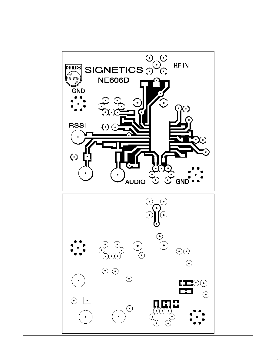
15
KTDN9/91
NE606
*Applies to Stand-Alone
data sheets only.
SR00365
Figure 18. SA606D SOL Product Board Layout (2X Actual Size* -- For Reference Use Only)
Philips Semiconductors
Product specification
SA606
Low-voltage high performance mixer FM IF system
1997 Nov 07
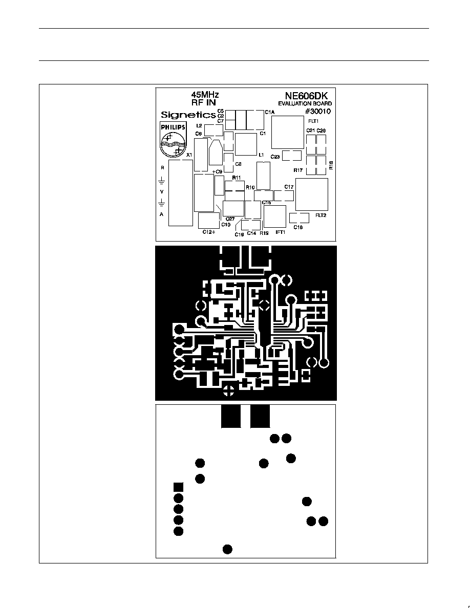
16
606 Silk Screen
606 BOTTOM
606 TOP
NOTE;
All views are TOP VIEW and
not actual size. For reference only.
SR00366
Figure 19.

Philips Semiconductors
Product specification
SA606
Low-voltage high-performance mixer FM IF system
1997 Nov 07
17
SO20:
plastic small outline package; 20 leads; body width 7.5 mm
SOT163-1
Philips Semiconductors
Product specification
SA606
Low-voltage high-performance mixer FM IF system
1997 Nov 07
18
SSOP20:
plastic shrink small outline package; 20 leads; body width 4.4 mm
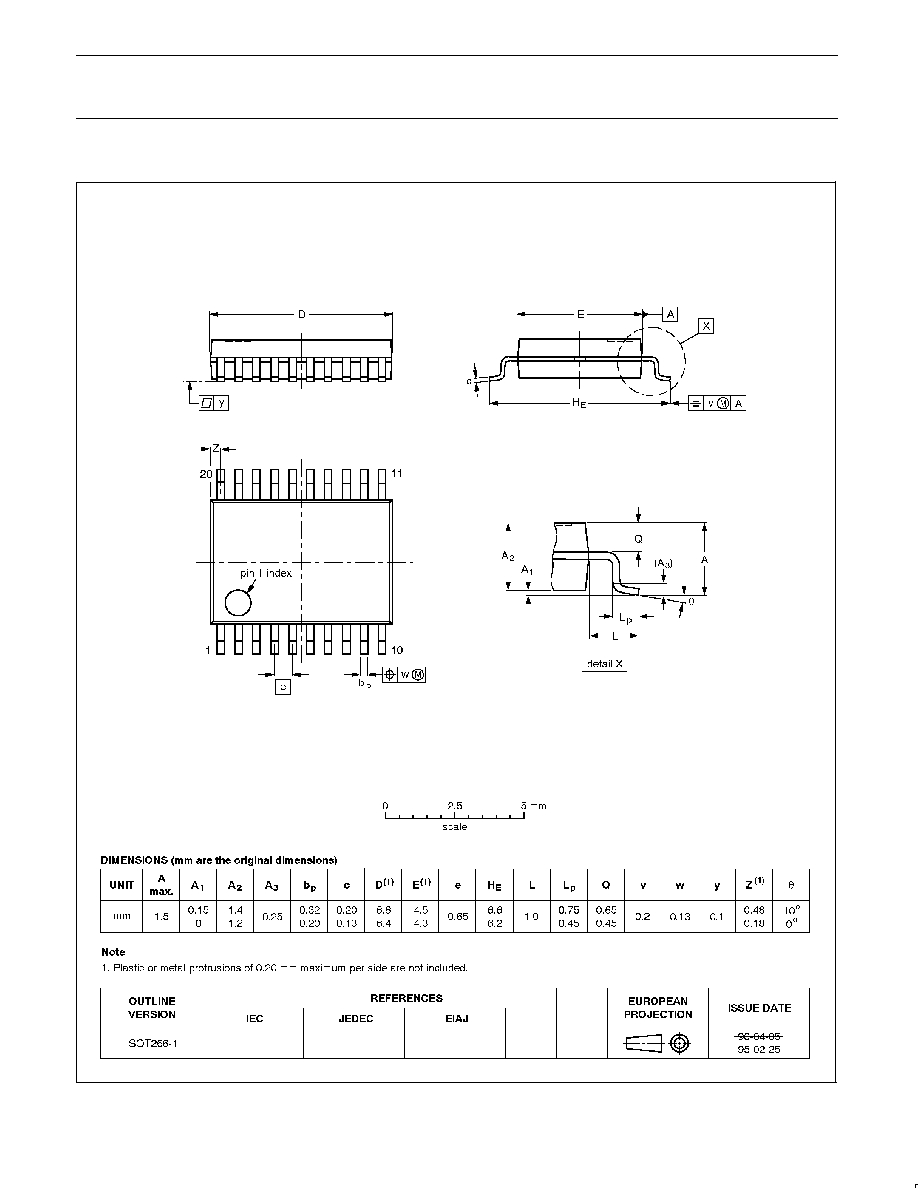
SOT266-1

Philips Semiconductors
Product specification
SA606
Low-voltage high-performance mixer FM IF system
1997 Nov 07
19
Philips Semiconductors and Philips Electronics North America Corporation reserve the right to make changes, without notice, in the products,
including circuits, standard cells, and/or software, described or contained herein in order to improve design and/or performance. Philips
Semiconductors assumes no responsibility or liability for the use of any of these products, conveys no license or title under any patent, copyright,
or mask work right to these products, and makes no representations or warranties that these products are free from patent, copyright, or mask
work right infringement, unless otherwise specified. Applications that are described herein for any of these products are for illustrative purposes
only. Philips Semiconductors makes no representation or warranty that such applications will be suitable for the specified use without further testing
or modification.
LIFE SUPPORT APPLICATIONS
Philips Semiconductors and Philips Electronics North America Corporation Products are not designed for use in life support appliances, devices,
or systems where malfunction of a Philips Semiconductors and Philips Electronics North America Corporation Product can reasonably be expected
to result in a personal injury. Philips Semiconductors and Philips Electronics North America Corporation customers using or selling Philips
Semiconductors and Philips Electronics North America Corporation Products for use in such applications do so at their own risk and agree to fully
indemnify Philips Semiconductors and Philips Electronics North America Corporation for any damages resulting from such improper use or sale.
This data sheet contains preliminary data, and supplementary data will be published at a later date. Philips
Semiconductors reserves the right to make changes at any time without notice in order to improve design
and supply the best possible product.
Philips Semiconductors
811 East Arques Avenue
P.O. Box 3409
Sunnyvale, California 94088≠3409
Telephone 800-234-7381
DEFINITIONS
Data Sheet Identification
Product Status
Definition
Objective Specification
Preliminary Specification
Product Specification
Formative or in Design
Preproduction Product
Full Production
This data sheet contains the design target or goal specifications for product development. Specifications
may change in any manner without notice.
This data sheet contains Final Specifications. Philips Semiconductors reserves the right to make changes
at any time without notice, in order to improve design and supply the best possible product.
©
Copyright Philips Electronics North America Corporation 1997
All rights reserved. Printed in U.S.A.
Philips
Semiconductors