 | –≠–ª–µ–∫—Ç—Ä–æ–Ω–Ω—ã–π –∫–æ–º–ø–æ–Ω–µ–Ω—Ç: SA611DH | –°–∫–∞—á–∞—Ç—å:  PDF PDF  ZIP ZIP |
Document Outline
- DESCRIPTION
- FEATURES
- PIN CONFIGURATION
- APPLICATIONS
- ORDERING INFORMATION
- BLOCK DIAGRAM
- ABSOLUTE MAXIMUM RATINGS
- RECOMMENDED OPERATING CONDITIONS
- DC ELECTRICAL CHARACTERISTICS
- AC ELECTRICAL CHARACTERISTICS
- PERFORMANCE CHARACTERISTICS
- PACKAGE OUTLINE
- Data sheet status
- Definitions
- Disclaimers
Philips
Semiconductors
SA611
1GHz low voltage LNA and mixer
Product specification
Supersedes data of 1997 Nov 07
IC17 Data Handbook
1999 Mar 26
INTEGRATED CIRCUITS
Philips Semiconductors
Product specification
SA611
1GHz low voltage LNA and mixer
2
1999 Mar 26
853-1886 21103
DESCRIPTION
The SA611 is a combined low-noise amplifier, and mixer designed
for high-performance low-power communication systems from
800-1000MHz. The low-noise preamplifier has a 1.7dB noise figure
at 881MHz with 15dB gain and an IP3 intercept of -7dBm at the
input. The gain is stabilized by on-chip compensation to vary less
than
±
0.2dB over -40 to +85
∞
C temperature range. The
wide-dynamic-range mixer has a 12dB noise figure and IP3 of
+7.0dBm at the input at 881MHz. The nominal current drawn from a
single 3V supply is 8.3mA. Additionally, the entire circuit can be
powered down to further reduce the supply current to less than
20
µ
A.
FEATURES
∑
Low current consumption
∑
Outstanding gain and noise figure
∑
Excellent gain stability versus temperature and supply voltage
∑
LNA and mixer power down capability
PIN CONFIGURATION
1
2
3
4
5
6
7
8
9
10
11
12
13
14
20
19
18
17
16
15
GND
LNA OUT
VCC
LNA IN
GND
GND
MIXER IN
MIXER OUT
MIXER OUT
GND
GND
GND
GND
GND
GND
GND
LO OUT
PD2
PD1
GND
SR00124
Figure 1. Pin Configuration
APPLICATIONS
∑
900MHz cellular and cordless front-end
∑
Spread spectrum receivers
∑
RF data links
∑
UHF frequency conversion
∑
Portable radio
ORDERING INFORMATION
DESCRIPTION
TEMPERATURE RANGE
ORDER CODE
DWG #
20-Pin Shrink Small Outline Package (Surface-mount, SSOP)
-40 to +85
∞
C
SA611DK
SOT266≠1
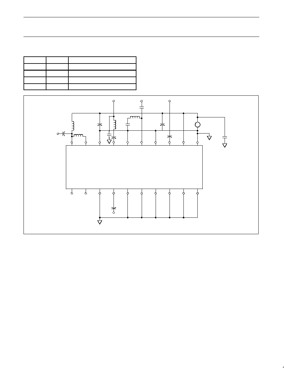
BLOCK DIAGRAM
4
3
2
1
5
20
19
18
17
16
7
6
10
9
8
15
14
13
12
11
LO
GND
GND
GND
V
CC
LNA
IN
GND
MIXER
IN
MIXER
OUT
MIXER
OUT
PD1
PD2
GND
LNA
OUT
GND
OUT
GND
GND
LNA
GND
GND
GND
SR00125
10pF
10pF
Figure 2. SA611 Block Diagram
Philips Semiconductors
Product specification
SA611
1GHz low voltage LNA and mixer
1999 Mar 26
3
ABSOLUTE MAXIMUM RATINGS
SYMBOL
PARAMETER
RATING
UNITS
V
CC
Supply voltage
NO TAG
-0.3 to +6
V
V
IN
Voltage applied to any other pin
-0.3 to (V
CC
+ 0.3)
V
P
D
Power dissipation, T
A
= 25
∞
C (still air)NO TAG
20-Pin Plastic SSOP
980
mW
T
JMAX
Maximum operating junction temperature
150
∞
C
P
MAX
Maximum power input/output
+20
dBm
T
STG
Storage temperature range
≠65 to +150
∞
C
NOTE:
1. Transients exceeding 8V on V
CC
pin may damage product.
2. Maximum dissipation is determined by the operating ambient temperature and the thermal resistance,
JA
: 20-Pin SSOP
= 110
∞
C/W
3. Pins 19 and 20 are ESD sensitive (mixer outputs).
RECOMMENDED OPERATING CONDITIONS
SYMBOL
PARAMETER
RATING
UNITS
V
CC
Supply voltage
2.7 to 5.5
V
T
A
Operating ambient temperature range
-40 to +85
∞
C
T
J
Operating junction temperature
-40 to +105
∞
C
DC ELECTRICAL CHARACTERISTICS
V
CC
= +3.0V, T
A
= 25
∞
C; unless otherwise stated.
SYMBOL
PARAMETER
TEST CONDITIONS
LIMITS
UNITS
SYMBOL
PARAMETER
TEST CONDITIONS
MIN
TYP
MAX
UNITS
Full power-on
8.3
mA
I
CC
Supply current
LNA powered-down
5 2
mA
I
CC
Su
ly current
LNA owered-down
5.2
mA
Full power-down
20
µ
A
V
T
PD logic threshold voltage
1.2
1.6
1.8
V
V
IH
Logic 1 level
2.0
V
CC
V
V
IL
Logic 0 level
≠0.3
0.8
V
I
IL
PD1 input current
Enable = 0.4V
10
µ
A
I
IH
PD2 input current
Enable = 2.4V
10
µ
A
Philips Semiconductors
Product specification
SA611
1GHz low voltage LNA and mixer
1999 Mar 26
4
AC ELECTRICAL CHARACTERISTICS
V
CC
= +3.0V, T
A
= 25
∞
C; RF
IN
= 881MHz, f
VCO
= 964MHz; unless otherwise stated.
SYMBOL
PARAMETER
TEST CONDITIONS
LIMITS
UNITS
SYMBOL
PARAMETER
TEST CONDITIONS
≠3
s
TYP
+3
s
UNITS
Low Noise Amplifier
f
RF
RF input frequency range
800
1000
MHz
S
21
Amplifier gain
15
dB
S
21
Amplifier gain in power-down mode
-28
dB
S
21
/
T
Gain temperature sensitivity enabled
0.006
dB/
∞
C
S
21
/
f
Gain frequency variation
800MHz - 1.0GHz
±
0.013
dB/MHz
S
12
Amplifier reverse isolation
@ 881 MHz
-28
dB
S
11
Amplifier input match
With ext. impedance matching
-10
dB
S
22
Amplifier output match
-10
dB
P
-1dB
Amplifier input 1dB gain compression
-20
dBm
IP3
Amplifier input third order intercept
-7
dBm
NF
Amplifier noise figure
1.7
dB
t
ON
Amplifier turn-on time (Enable Lo
Hi)
120
µ
s
t
OFF
Amplifier turn-off time (Enable Hi
Lo)
0.3
µ
s
Mixer
PG
C
Mixer power conversion gain: R
P
= R
L
= 1.2k
,
f
RF
= 881MHz, f
LO
= 964MHz,
f
IF
= 83MHz
8.7
dB
S
11M
Mixer input match
Ext. impedance matching req.
-10
dB
NF
M
Mixer SSB noise figure
12
dB
P
-1dB
Mixer input 1dB gain compression
-14.5
dBm
IP3
M
Mixer input third order intercept
7.0
dBm
IP
2INT
Mixer input second order intercept
15
dBm
P
RFM-IF
Mixer RF feedthrough
RF
IN
= -28dBm
-45
dBm
P
LO-IF
LO feedthrough to IF
LO = -0dBm
-23
dBm
P
LO-RFM
LO to mixer input feedthrough
-36
dBm
P
LO-RF
LO to LNA input feedthrough
-38
dBm
Overall System
G
SYS
System gain
LNA + Mixer
23.0
23.7
24.4
dB
Philips Semiconductors
Product specification
SA611
1GHz low voltage LNA and mixer
1999 Mar 26
5
Table 1.
Power ON/OFF Control Logic
PD1
PD2
0
0
Full chip power-down
0
1 or open
Mixer on, LNA power-down
1 or open
0
Standby (bias on)
1 or open
1 or open
Full chip power-on (default)
SR00126
+
≠
20
19
18
17
16
15
14
13
12
11
1
2
3
4
5
6
7
8
9
10
PD1
PD2
GND
GND
GND
GND
GND
GND
GND
MIXER
GND
GND
GND
GND
V
CC
LO
OUT
IF
OUT
VCO
OUT
SA611
C3
6.8pF
L1
560nH
L4
560nH
C2
10nF
C14
6.8pF
C13
33pF
C8
10nF
3V
C12
100pF
C1
100pF
V
CC
OUT
MIXER
OUT
MIXER
IN
LNA
IN
LNA
OUT
L3
6.8nH
10nF
0.1
µ
F
C9
C11
L6
12nH
C10
2.2pF
Figure 3. SA611 Applications Circuit
Philips Semiconductors
Product specification
SA611
1GHz low voltage LNA and mixer
1999 Mar 26
6
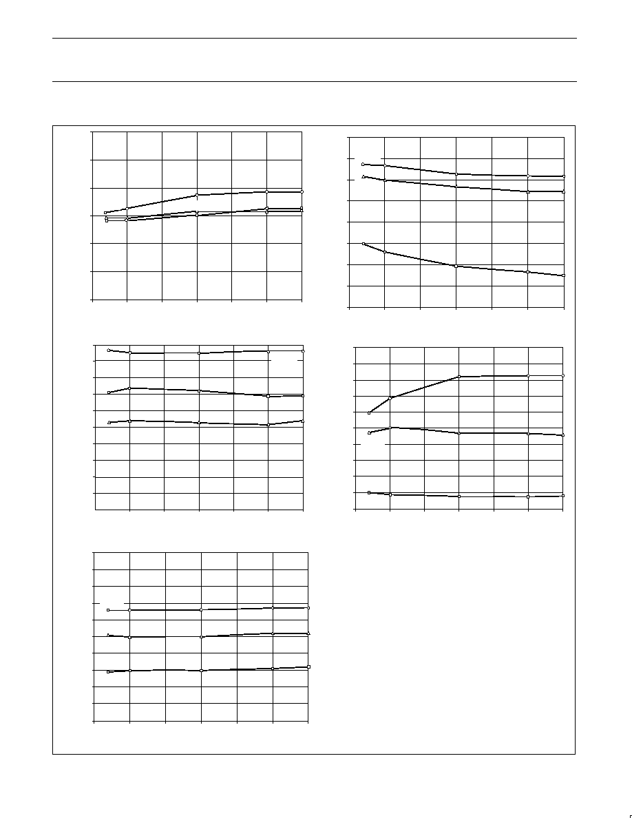
PERFORMANCE CHARACTERISTICS
-15
2.5
3
3.5
4
4.5
5
5.5
V
CC
(V)
LNA
1dB (dBm)
-40
∞
C
25
∞
C
LNA 1dB Compression vs V
CC
-16
-17
-18
-19
-20
-21
-22
-23
-24
-25
-14.0
2.5
3
3.5
4
4.5
5
5.5
V
CC
(V)
MIXER 1dB (dBm)
-40
∞
C
25
∞
C
85
∞
C
Mixer 1dB Compression vs V
CC
-14.5
-15.0
-15.5
-16.0
-13.0
-13.5
-28.0
2.5
3
3.5
4
4.5
5
5.5
V
CC
(V)
LNA
GAIN (dB)
-40
∞
C
25
∞
C
85
∞
C
LNA Gain (Disabled) vs V
CC
-28.5
-29.0
-29.5
-30.0
-30.5
-31.0
-27.0
-27.5
10.0
2.5
3
3.5
4
4.5
5
5.5
V
CC
(V)
MIXER IP3 (dBm)
-40
∞
C
25
∞
C
85
∞
C
Mixer IP3 vs V
CC
9.0
8.0
7.0
6.0
5.0
4.0
3.0
2.0
-11
2.5
3
3.5
4
4.5
5
5.5
V
CC
(V)
LNA
IP3 (dBm)
-40
∞
C
25
∞
C
LNA IP3 vs V
CC
-2
-3
-4
-5
-6
-7
-8
-9
-10
0
85
∞
C
85
∞
C
SR01249
-12
1.0
0.0
Figure 4.
Philips Semiconductors
Product specification
SA611
1GHz low voltage LNA and mixer
1999 Mar 26
7
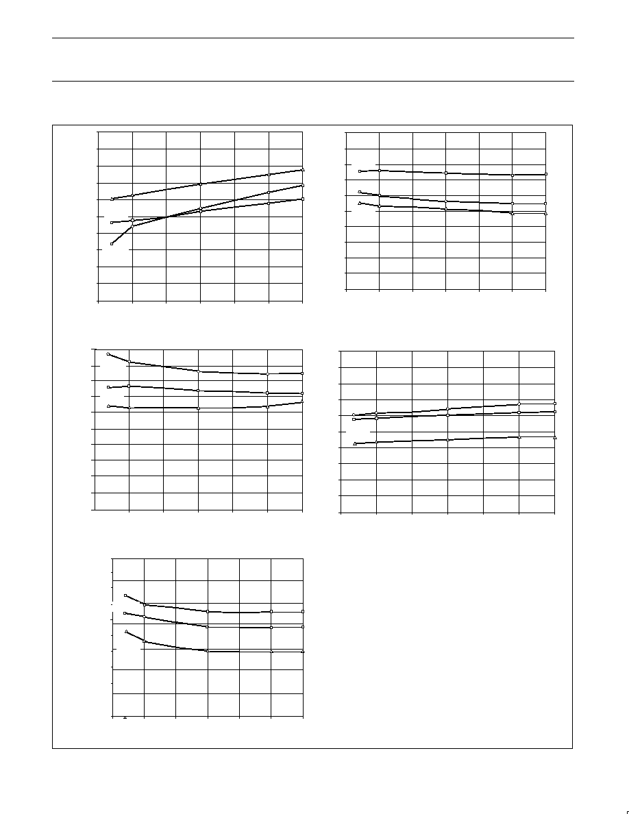
PERFORMANCE CHARACTERISTICS
2.5
3
3.5
4
4.5
5
5.5
V
CC
(V)
Icc (mA)
-40
∞
C
25
∞
C
85
∞
C
I
CC
vs V
CC
and Temperature
8.2
7.8
7.4
7.0
6.6
6.2
5.8
9.8
9.4
9.0
8.6
2.5
3
3.5
4
4.5
5
5.5
V
CC
(V)
MIXER GAIN (dB)
-40
∞
C
85
∞
C
Mixer Power Gain vs V
CC
2.5
3
3.5
4
4.5
5
5.5
V
CC
(V)
LO to LNA
IN (dBm)
-40
∞
C
25
∞
C
85
∞
C
LO to LNA In Feedthrough vs V
CC
2.5
3
3.5
4
4.5
5
5.5
V
CC
(V)
LO to MIXER IN (dBm)
-40
∞
C
LO to Mixer In Feedthrough vs V
CC
-35
-36
-37
-38
-39
-40
-41
-42
-43
-44
-45
2.5
3
3.5
4
4.5
5
5.5
V
CC
(V)
LO to IF (dBm)
-40
∞
C
25
∞
C
85
∞
C
LO to IF Feedthrough vs V
CC
-20
-21
-22
-23
-24
-25
-26
-27
-28
-29
-30
SR01250
10.0
9.5
9.0
8.5
8.0
7.5
7.0
6.5
6.0
5.5
5.0
25
∞
C
≠31.0
≠33.0
≠35.0
≠37.0
≠39.0
≠41.0
≠43.0
≠45.0
25
∞
C
85
∞
C
Figure 5.
Philips Semiconductors
Product specification
SA611
1GHz low voltage LNA and mixer
1999 Mar 26
8
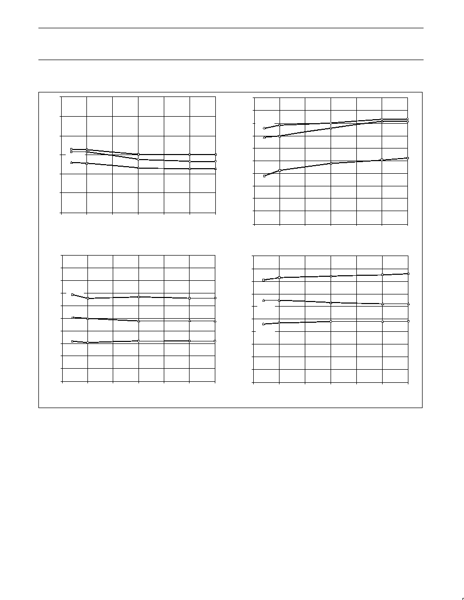
PERFORMANCE CHARACTERISTICS
2.5
3
3.5
4
4.5
5
5.5
V
CC
(V)
MIXER IN to IF (dBm)
-40
∞
C
25
∞
C
85
∞
C
Mixer In to IF Feedthrough vs V
CC
15.0
2.5
3
3.5
4
4.5
5
5.5
V
CC
(V)
LNA
GAIN (dB)
-40
∞
C
25
∞
C
85
∞
C
LNA Gain (Enabled) vs V
CC
14.8
14.6
14.4
14.2
14.0
13.8
13.6
15.6
15.4
15.2
2.5
3
3.5
4
4.5
5
5.5
V
CC
(V)
MIXER NOISE FIGURE (dB)
-40
∞
C
25
∞
C
85
∞
C
Mixer Noise Figure vs V
CC
12.8
12.4
12.3
12.2
12.1
12.0
11.4
11.3
11.2
11.1
11.0
2.5
3
3.5
4
4.5
5
5.5
V
CC
(V)
LNA
NOISE FIGURE (dB)
-40
∞
C
25
∞
C
85
∞
C
LNA Noise Figure vs V
CC
2.0
1.9
1.8
1.7
1.6
1.5
1.4
1.3
1.2
1.1
1.0
SR01251
≠42.0
≠43.0
≠44.0
≠45.0
≠46.0
≠47.0
≠48.0
Figure 6.
Philips Semiconductors
Product specification
SA611
1GHz low voltage LNA and mixer
1999 Mar 26
9
CH2
S
11
1 U FS
3
2
1
4
1:
40.1
-129.6
200 MHz
2:
24.0
-62.9
400 MHz
3:
18.6
-37.4
600 MHz
START
100. 000 000 MHz
STOP
1 200. 000 000 MHz
SR01252
4:
14.1
10.5 pF
-16.7
900 MHz
3
CH1
S
22
1 U FS
2
1
4
1:
40.5
-28.2
700 MHz
2:
36.1
-12.4
800 MHz
3:
34.7
3.5
900 MHz
START
700. 000 000 MHz
STOP
1 200. 000 000 MHz
4:
34.9
3.74
661.4 pH
900 MHz
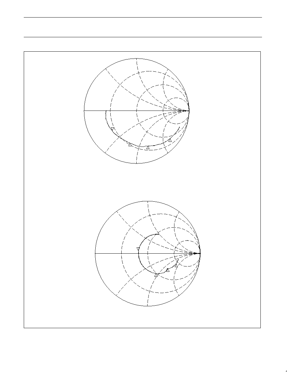
A. S11 DATA
B. S22 DATA
Figure 7. Typical S
11
of LNA at 3V
Philips Semiconductors
Product specification
SA611
1GHz low voltage LNA and mixer
1999 Mar 26
10
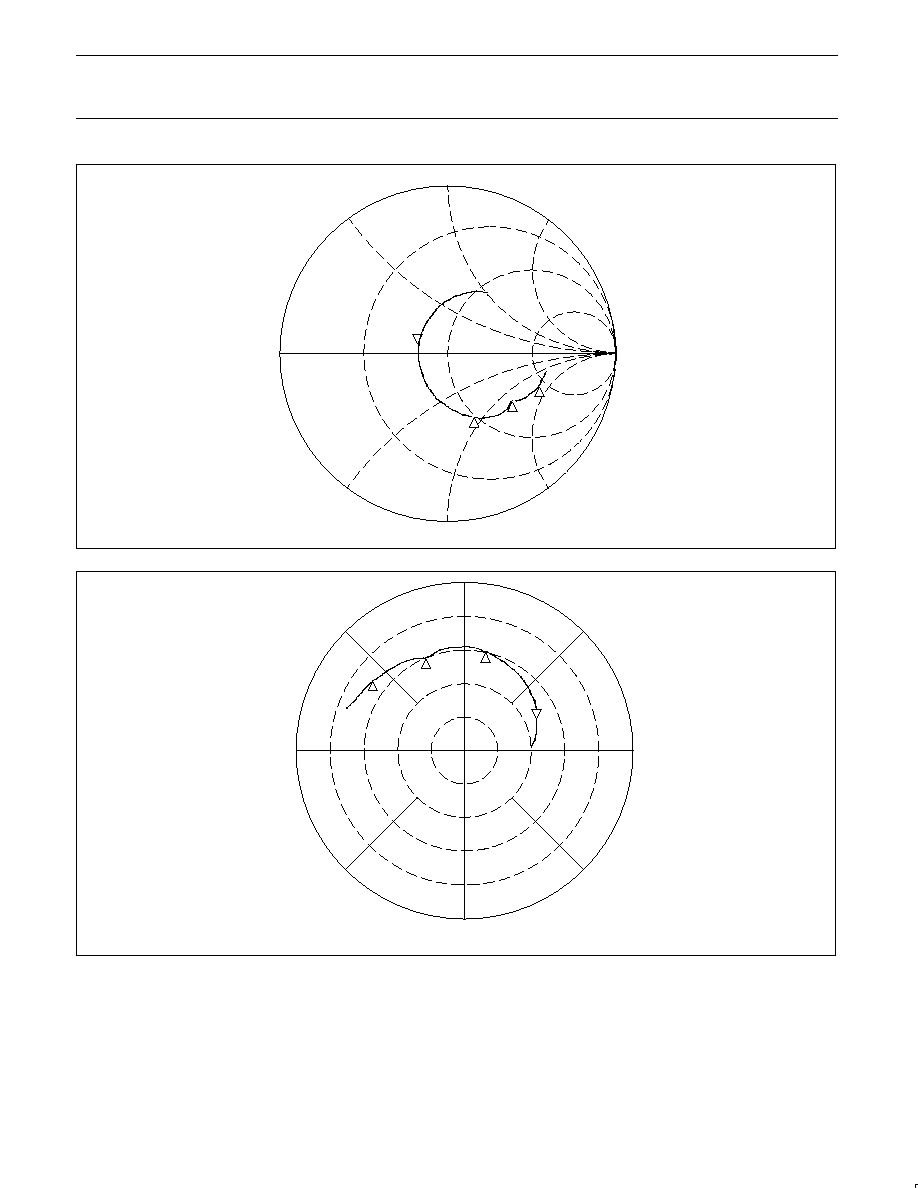
3
CH1
S
22
1 U FS
2
1
4
1:
40.5
-28.2
700 MHz
2:
36.1
-12.4
800 MHz
3:
34.7
3.5
900 MHz
START
700. 000 000 MHz
STOP
1 200. 000 000 MHz
SR01253
4:
34.9
3.74
661.4 pH
900 MHz
Figure 8. Typical S
22
of LNA at 3V
CH1
S
21
10 U FS
1:
6.7 U
142.5
∞
200 MHz
2:
5.9 U
112.3
∞
400 MHz
3:
5.9 U
78.1
∞
600 MHz
START
100. 000 000 MHz
STOP
1 200. 000 000 MHz
1
3
2
4
SR01254
4:
4.5 U
21.2
∞
900 MHz
Figure 9. Typical S
21
of LNA at 3V
Philips Semiconductors
Product specification
SA611
1GHz low voltage LNA and mixer
1999 Mar 26
11
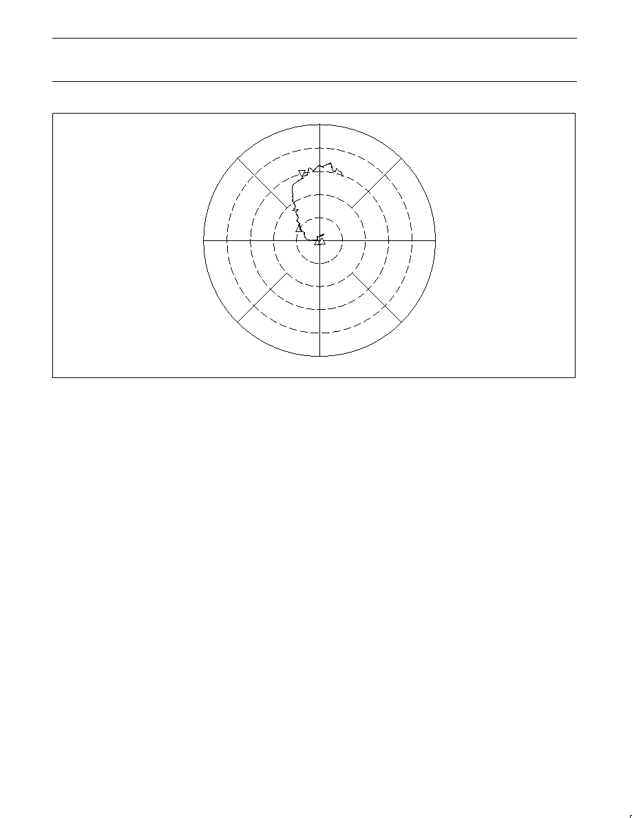
CH2
S
12
50 mU FS
1:
1.9 mU
83.0
∞
200 MHz
2:
1.6 mU
133.5
∞
400 MHz
3:
11.4 mU
141.5
∞
600 MHz
START
100. 000 000 MHz
STOP
1 200. 000 000 MHz
3
2
4
SR01255
1
4:
27.9 mU
106.1
∞
900 MHz
Figure 10. Typical S
12
of LNA at 3V

Philips Semiconductors
Product specification
SA611
1GHz low voltage LNA and mixer
1999 Mar 26
12
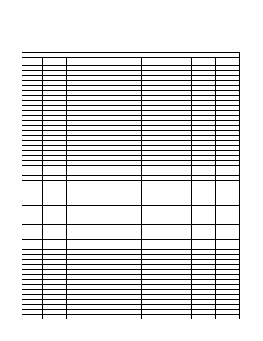
3
CH1
S
11
1 U FS
2
1
4
1:
122.8
-144.9
200 MHz
2:
58.0
-86.8
400 MHz
3:
45.9
-62.3
600 MHz
START
100. 000 000 MHz
STOP
1 200. 000 000 MHz
SR01256
4:
26.6
-43.2
4.085 pF
900 MHz
Figure 11. Typical S
11
of Mixer at 3V
Philips Semiconductors
Product specification
SA611
1GHz low voltage LNA and mixer
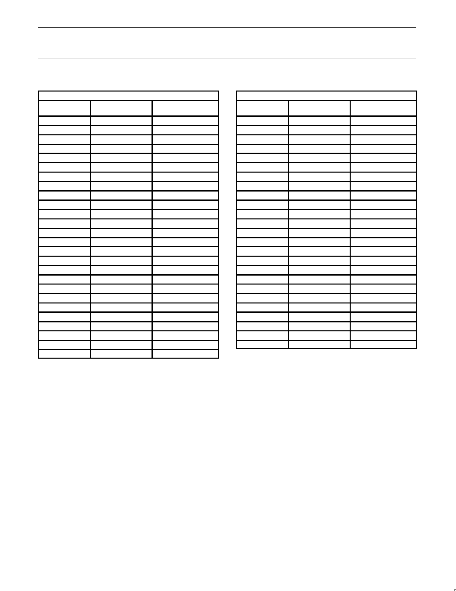
1999 Mar 26
13
Table 2.
Typical S-Parameters of LNA at 3V
LNA
Freq (MHz)
|S
11
|
(U)
<S
11
(deg)
|S
21
|
(U)
<S
21
(deg)
|S
12
|
(U)
<S
12
(deg)
|S
22
|
(U)
<S
22
(deg)
100
0.86
-20
7.4
160
0.001
91.91
0.59
-9.62
122
0.86
-24
7.1
156
0.001
62
0.58
-11.71
144
0.85
-28
7.0
151
0.001
105.42
0.58
-13.86
166
0.83
-32
6.9
148
0.000
91.65
0.57
-15.89
188
0.82
-36
6.8
144
0.002
100.23
0.57
-17.80
210
0.81
-41
6.7
140
0.002
73.57
0.56
-20.05
232
0.80
-45
6.6
136
0.002
99.70
0.55
-22.37
254
0.79
-48
6.5
133
0.001
84.00
0.54
-24.60
276
0.78
-52
6.4
130
0.001
103.18
0.53
-26.89
298
0.76
-56
6.3
126
0.002
94.33
0.52
-28.72
320
0.75
-59
6.3
123
0.002
66.98
0.51
-30.98
342
0.73
-63
6.2
119
0.002
108.53
0.50
-32.79
364
0.71
-66
6.1
116
0.002
118.13
0.48
-34.68
386
0.70
-69
6.0
113
0.001
103.4
0.47
-36.06
408
0.69
-72
5.9
111
0.001
175.94
0.46
-36.64
430
0.68
-76
5.9
109
0.004
174.1
0.45
-37.21
452
0.69
-78
6.0
106
0.006
162.02
0.46
-38.41
474
0.68
-82
6.1
102
0.007
160.07
0.47
-41.54
496
0.67
-85
6.1
97
0.008
153.6
0.47
-45.75
518
0.66
-89
6.1
93
0.010
146.17
0.46
-50.35
540
0.65
-92
6.1
89
0.009
142.13
0.45
-54.73
562
0.63
-96
6.1
85
0.010
138.49
0.43
-59.16
584
0.62
-99
6.0
81
0.011
146.17
0.42
-63.93
606
0.62
-102
5.9
77
0.011
140.55
0.40
-68.56
628
0.61
-104
5.8
72
0.013
137.2
0.38
-73.48
650
0.61
-107
5.7
69
0.013
130.62
0.36
-78.19
672
0.60
-109
5.7
65
0.016
129.77
0.34
-83.75
694
0.60
-112
5.6
61
0.016
131.94
0.31
-89.81
716
0.59
-115
5.5
57
0.017
128.67
0.29
-96.92
738
0.59
-118
5.5
53
0.019
127.53
0.27
-104.48
760
0.59
-121
5.3
48
0.021
123.42
0.24
-112.81
782
0.59
-124
5.3
44
0.021
122.31
0.22
-122.41
804
0.59
-126
5.1
40
0.022
119.52
0.21
-132.81
826
0.59
-129
5.0
36
0.024
118.29
0.19
-145.39
848
0.59
-132
4.9
31
0.026
115.98
0.18
-159.13
870
0.59
-135
4.8
26
0.027
111.9
0.17
-175.11
892
0.59
-138
4.6
22
0.028
108.11
0.18
169.02
914
0.59
-142
4.5
18
0.028
105.92
0.19
154.96
936
0.59
-144
4.3
14
0.028
106.13
0.20
141.94
958
0.59
-148
4.2
9
0.030
99.79
0.22
130.27
980
0.59
-151
4.0
4
0.031
99.30
0.24
119.5
1002
0.59
-153
3.8
0
0.031
94.81
0.26
110.61
1024
0.59
-157
3.6
-2
0.032
90.91
0.28
102.16
1046
0.59
-160
3.5
-6
0.032
85.65
0.30
94.98
1068
0.59
-164
3.3
-10
0.033
86.10
0.33
88.45
1090
0.59
-167
3.2
-14
0.033
80.59
0.35
82.47
1112
0.59
-170
3.0
-18
0.031
79.18
0.36
77.17
1134
0.58
-172
2.8
-22
0.030
46.32
0.38
71.98
1156
0.58
-175
2.7
-25
0.031
78.57
0.39
67.45
1178
0.57
-178
2.5
-28
0.031
73.66
0.41
62.73
1200
0.57
178
2.4
-31
0.029
71.78
0.42
58.87
Philips Semiconductors
Product specification
SA611
1GHz low voltage LNA and mixer
1999 Mar 26
14
Table 3.
Typical S-Parameters of Mixer at 3V
Mixer
Freq (MHz)
|S
11
|
(U)
<S
11
(deg)
100
0.73
-11
122
0.73
-147
144
0.72
-16
166
0.72
-19
188
0.72
-21
210
0.71
-24
232
0.70
-27
254
0.70
-29
276
0.69
-32
298
0.68
-34
320
0.67
-37
342
0.66
-39
364
0.64
-42
386
0.63
-≠44
408
0.62
-46
430
0.61
-48
452
0.59
-50
474
0.58
-52
496
0.57
-53
518
0.56
-54
540
0.55
-56
562
0.55
-57
584
0.54
-59
606
0.54
-61
628
0.54
-62
650
0.54
-64
Mixer
Freq (MHz)
|S
11
|
(U)
<S
11
(deg)
672
0.54
-65
694
0.54
-67
716
0.54
-69
738
0.54
-71
760
0.54
-73
782
0.55
-76
804
0.55
-78
826
0.55
-80
848
0.55
-82
870
0.55
-85
892
0.56
-87
914
0.55
-90
936
0.56
-93
958
0.56
-96
980
0.56
-98
1002
0.56
-101
1024
0.57
-104
1046
0.57
-106
1068
0.57
-110
1090
0.57
-112
1112
0.57
-115
1134
0.57
-118
1156
0.57
-121
1178
0.57
-124
1200
0.57
-127
Philips Semiconductors
Product specification
SA611
1GHz low voltage LNA and mixer
1999 Mar 26
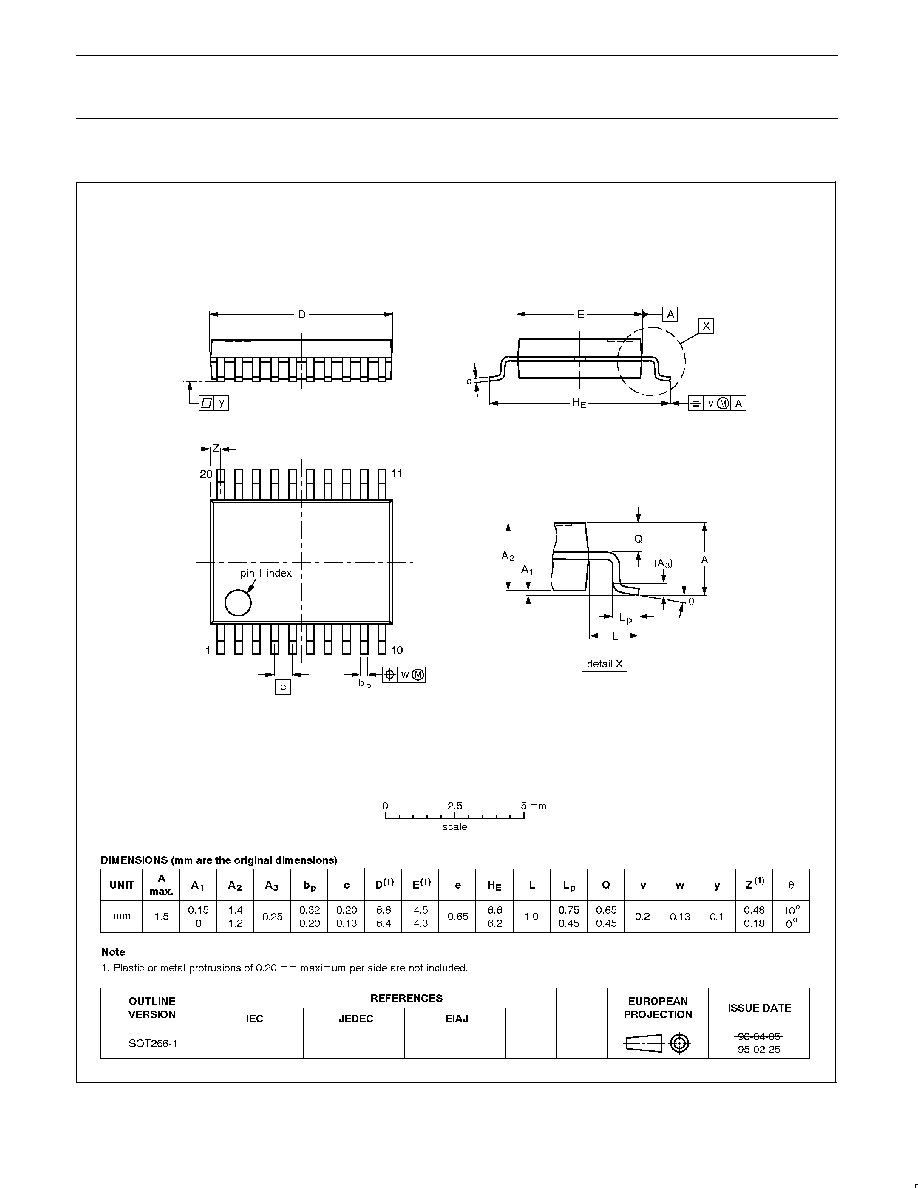
15
SSOP20:
plastic shrink small outline package; 20 leads; body width 4.4 mm
SOT266-1
Philips Semiconductors
Product specification
SA611
1GHz low voltage LNA and mixer
1999 Mar 26
16
Definitions
Short-form specification -- The data in a short-form specification is extracted from a full data sheet with the same type number and title. For
detailed information see the relevant data sheet or data handbook.
Limiting values definition -- Limiting values given are in accordance with the Absolute Maximum Rating System (IEC 134). Stress above one
or more of the limiting values may cause permanent damage to the device. These are stress ratings only and operation of the device at these or
at any other conditions above those given in the Characteristics sections of the specification is not implied. Exposure to limiting values for extended
periods may affect device reliability.
Application information -- Applications that are described herein for any of these products are for illustrative purposes only. Philips
Semiconductors make no representation or warranty that such applications will be suitable for the specified use without further testing or
modification.
Disclaimers
Life support -- These products are not designed for use in life support appliances, devices or systems where malfunction of these products can
reasonably be expected to result in personal injury. Philips Semiconductors customers using or selling these products for use in such applications
do so at their own risk and agree to fully indemnify Philips Semiconductors for any damages resulting from such application.
Right to make changes -- Philips Semiconductors reserves the right to make changes, without notice, in the products, including circuits, standard
cells, and/or software, described or contained herein in order to improve design and/or performance. Philips Semiconductors assumes no
responsibility or liability for the use of any of these products, conveys no license or title under any patent, copyright, or mask work right to these
products, and makes no representations or warranties that these products are free from patent, copyright, or mask work right infringement, unless
otherwise specified.
Philips Semiconductors
811 East Arques Avenue
P.O. Box 3409
Sunnyvale, California 94088≠3409
Telephone 800-234-7381
©
Copyright Philips Electronics North America Corporation 1999
All rights reserved. Printed in U.S.A.
Date of release: 03-99
Document order number:
9397 750 05473
Philips
Semiconductors
Data sheet
status
Objective
specification
Preliminary
specification
Product
specification
Product
status
Development
Qualification
Production
Definition
[1]
This data sheet contains the design target or goal specifications for product development.
Specification may change in any manner without notice.
This data sheet contains preliminary data, and supplementary data will be published at a later date.
Philips Semiconductors reserves the right to make chages at any time without notice in order to
improve design and supply the best possible product.
This data sheet contains final specifications. Philips Semiconductors reserves the right to make
changes at any time without notice in order to improve design and supply the best possible product.
Data sheet status
[1]
Please consult the most recently issued datasheet before initiating or completing a design.