 | –≠–ª–µ–∫—Ç—Ä–æ–Ω–Ω—ã–π –∫–æ–º–ø–æ–Ω–µ–Ω—Ç: SA637 | –°–∫–∞—á–∞—Ç—å:  PDF PDF  ZIP ZIP |
Document Outline
- DESCRIPTION
- FEATURES
- APPLICATIONS
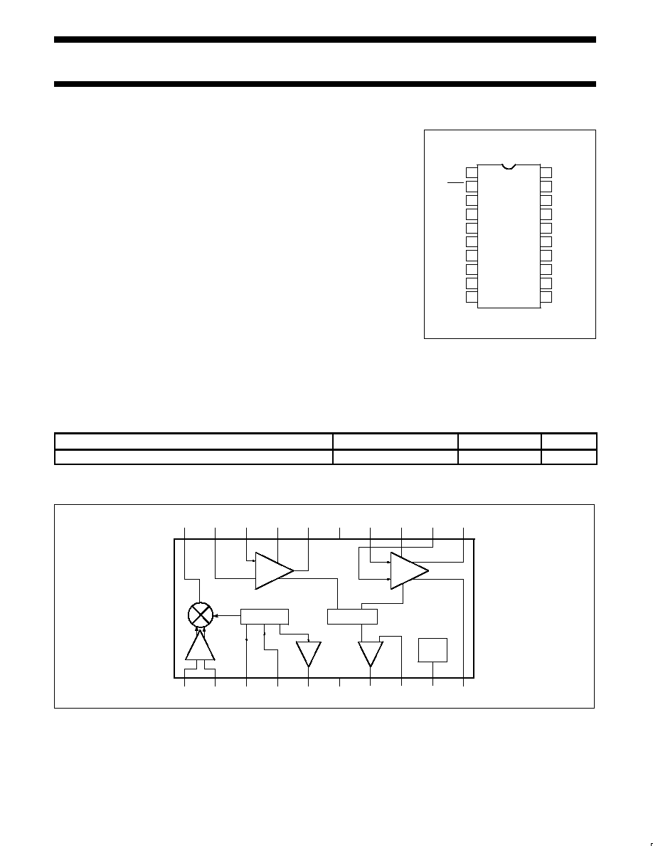
- PIN CONFIGURATION
- ORDERING INFORMATION
- BLOCK DIAGRAM
- ABSOLUTE MAXIMUM RATINGS
- DC ELECTRICAL CHARACTERISTICS
- AC ELECTRICAL CHARACTERISTICS
- CIRCUIT DESCRIPTION
- Mixer
- Oscillator and Buffer
- IF Amplifier and IF Limiter
- RSSI
- DC Power Supply
- PERFORMANCE CHARACTERISTICS
- PIN FUNCTIONS
Philips Semiconductors RF Communications Products
Product specification
SA637
Low-voltage digital IF receiver
2
October 27, 1993
853-1718 11205
DESCRIPTION
The SA637 is a low-voltage high performance
monolithic digital system with high-speed
RSSI incorporating a mixer, oscillator with
buffered output, two limiting intermediate
frequency amplifiers, fast logarithmic
received signal strength indicator (RSSI),
voltage regulator, RSSI op amp and power
down pin. The SA637 is available in SSOP
(shrink small outline package).
The SA637 was designed for portable digital
communication applications and will function
down to 2.7V. The limiter amplifier has
differential outputs with 2MHz small signal
bandwidth. The RSSI output has access to
the feedback pin. This enables the designer
to level adjust the outputs or add filtering.
FEATURES
∑
V
CC
= 2.7 to 5.5V
∑
Low power receiver (3.8mA @ 3V)
∑
Power down mode (I
CC
= 110
µ
A)
∑
Fast RSSI rise and fall times
∑
Extended RSSI range with temperature
compensation
∑
RSSI op amp
∑
2MHz limiter small signal bandwidth
∑
455kHz filter matching (1.5k
)
∑
Differential limiter output
∑
Oscillator buffer
∑
SSOP-20 package
APPLICATIONS
∑
ADC (American Digital Cellular)
∑
Digital receiver systems
∑
Cellular radio
PIN CONFIGURATION
DK Packages
MIXER
OUTPUT
IF AMP IN
GND
LIMITER IN
LIM OUT (+)
RFIN
RFIN
OSC E
OSC B
OSC
BUFFER
RSSI
RSSI
FEEDBACK
POWER
DOWN
1
2
3
4
5
6
7
8
9
10
11
12
13
14
20
19
18
17
16
15
LIM OUT (-)
VCC
IF AMP
DECOUP
IF AMP
DECOUP
IF AMP OUT
LIMITER
DECOUP
LIMITER
DECOUP
ORDERING INFORMATION
DESCRIPTION
TEMPERATURE RANGE
ORDER CODE
DWG #
20-Pin Plastic Shrink Small Outline Package (Surface-mount)
-40 to +85
∞
C
SA637DK
1563
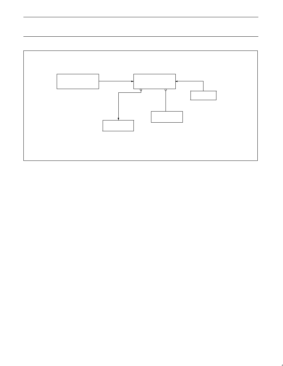
BLOCK DIAGRAM
OSCILLATOR
MIXER
+
≠
+ ≠
IF
AMP
20
19
18
17
16
15
14
13
12
11
1
2
3
4
5
6
7
8
9
10
E
B
LIMITER
VCC
GND
FAST RSSI
POWER
DOWN
Philips Semiconductors RF Communications Products
Product specification
SA637
Low-voltage digital IF receiver
October 27, 1993
3
ABSOLUTE MAXIMUM RATINGS
SYMBOL
PARAMETER
RATING
UNITS
V
CC
Supply voltage
-0.3 to +6.0
V
V
IN
Voltage applied to any other pin
-0.3 to (V
CC
+ 0.3)
V
T
STG
Storage temperature range
-65 to +150
∞
C
T
A
Operating ambient temperature range
-40 to +85
∞
C
NOTE: Thermal impedance (
JA
) = 117
∞
C/W
DC ELECTRICAL CHARACTERISTICS
V
CC
= +3V, T
A
= 25
∞
C; unless otherwise stated.
SYMBOL
PARAMETER
TEST CONDITIONS
LIMITS
UNITS
MIN
TYP
MAX
V
CC
Power supply voltage range
2.7
5.5
V
I
CC
DC current drain
Pin 9 = HIGH or OPEN
3.8
4.5
mA
V
CC
= 4.7V
4.4
5.5
mA
Standby
Pin 9 = LOW
0.11
0.5
mA
Input current
Pin 9 = LOW
-10
10
µ
A
Pin 9 = HIGH
-10
10
µ
A
Input level
Pin 9 = LOW
0
0.3V
CC
µ
A
Pin 9 = HIGH
0.7V
CC
V
CC
µ
A
t
ON
Power up time
RSSI valid (10% to 90%)
10
µ
s
t
OFF
Power down time
RSSI invalid (90% to 10%)
5
µ
s
AC ELECTRICAL CHARACTERISTICS
T
A
= 25
∞
C; V
CC
= +3V, unless otherwise stated. RF frequency = 90MHz; RF input step-up = +14.5dBV; IF frequency = 455kHz; RF level =
-68dBm. Test circuit Figure 1. The parameters listed below are tested using automatic test equipment to assure consistent electrical
characteristics. The limits do not represent the ultimate performance limits of the device. Use of an optimized RF layout will improve many of
the listed parameters.
SYMBOL
PARAMETER
TEST CONDITIONS
LIMITS
UNITS
MIN
TYP
MAX
Mixer/Osc section
f
IN
Input signal frequency
200
MHz
f
OSC
Crystal oscillator frequency
200
MHz
NF
Noise figure at 90MHz
Matched input and output
6.2
dB
TOI
Third-order input intercept point
Input matched to 50
source
-17
dBm
P1dB
Input 1dB compression point
-27
dBm
Conversion power gain
Matched 50
7
dB
R
IN
Mixer input resistance
2.5
k
C
IN
Mixer input capacitance
2.2
pF
R
OUT
Mixer output resistance
1.87
k
Buffered LO output level
LO = 447mV
P-P
, 1k
AC load
100
300
500
mV
P-P
IF section
IF amp power gain
50
source
36
dB
Limiter power gain
50
source
60
dB
IF
BW
IF amp bandwidth
2.5
MHz
Philips Semiconductors RF Communications Products
Product specification
SA637
Low-voltage digital IF receiver
October 27, 1993
4
AC ELECTRICAL CHARACTERISTICS
(Continued)
SYMBOL
PARAMETER
TEST CONDITIONS
LIMITS
UNITS
MIN
TYP
MAX
RF RSSI output
RF level = -118dBm
.01
0.2
.65
V
RF level = -68dBm
.4
0.9
1.7
V
RF level = -28dBm
1.0
1.7
2.3
V
RSSI range
90
dB
RSSI accuracy
±
1.5
dB
RSSI ripple
30
mV
P-P
RSSI speed
Rise time
No interstage filter
2.5
µ
s
With interstage filter
22
µ
s
RSSI speed
Fall time
No interstage filter
10
µ
s
With interstage filter
50
µ
s
IF input impedance
1.5
k
IF output impedance
1.5
k
Limiter input impedance
1.5
k
Limiter output impedance
(Pin 10, Pin 11)
200
Limiter output signal level
(Pin 10, Pin 11) 1.5k
AC load
280
mV
P-P
Limiter output DC level
1.27
V
Differential output matching
±
6
mV
Differential output offset
±
30
mV
CIRCUIT DESCRIPTION
Mixer
The mixer has a balanced input and is
capable of being driven single-ended. The
input impedance is 2.5k
in parallel with a
2.2pF cap at 90MHz RF. The mixer output
can drive a 1500
ceramic filter at 455kHz or
600kHz directly without any matching
required. The mixer conversion power gain is
7dB when both input and output are matched
and optimum LO level is used to drive the
internal mixer core.
Oscillator and Buffer
The on-board oscillator supplies the signal for
the mixer down-conversion. The internally
biased transistor can be configured as a
Colpitts or Butler overtone crystal oscillator.
The transistor's bias current can be
increased if desired by adding a shunt
resistor from Pin 3 to ground. The oscillator's
buffered output (Pin 5) can be used as a
feedback signal to lock the oscillator to an
appropriate reference.
IF Amplifier and IF Limiter
The IF strip provides more than 95dB of
power gain for the down converted signal. Its
overall bandwidth is limited to 2MHz. The
input and output impedance of the IF
amplifier and the input impedance of the IF
limiter are set to 1500
(match to 455kHz
filter). A second filter is connected between
the IF amplifier and the limiter for improved
channel selectivity and reduced instability.
This ceramic filter provides 3dB interstage
insertion loss which results in optimal RSSI
linearity. The overall gain can be reduced if
desired by adding an external attenuator after
the IF amplifier. The differential limiter
outputs (Pins 10 and 11) are available for
demodulator circuits.
RSSI
The received signal strength indicator
provides a linear voltage indication of the
received signal strength in dB for a range in
excess of 90dB. The response time to a
change in input signal is less than a few
microseconds and the delay is kept to a
minimum because of the use of a minimum
phase shift circuit. Because of the speed of
the RSSI circuit, the RSSI rise and fall time
may, in practice, be dominated by the
bandwidth of the external bandpass filter that
is placed between the mixer and the IF, and
the external filter placed between the IF
amplifier and limiter. Since the RSSI function
requires the signal to propagate through the
whole IF strip, and the rise and fall time of the
filters are inversely proportional to their
bandwidth, there is a trade-off between
channel selectivity and RSSI response. A
possible solution is to use a second SA637
with wider band external filters for faster
RSSI response.
The RSSI curve is temperature compensated
and in addition is designed for improved
consistency from unit to unit.
The RSSI circuit drives an on-chip low power
op amp with rail-to-rail output which can be
connected as a unity gain RSSI buffer or a
gain stage or even a comparator.
DC Power Supply
The IC is designed for operation between 2.7
and 5.5V. A power supply dependent biasing
scheme is used in the mixers to benefit from
the large headroom available at higher V
CC
s.
Philips Semiconductors RF Communications Products
Product specification
SA637
Low-voltage digital IF receiver
October 27, 1993
5
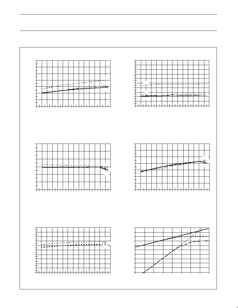
PERFORMANCE CHARACTERISTICS
Supply Current vs Temperature
and Supply Voltage
TEMPERATURE (
∞
C)
Power Down Supply Current vs Temperature
and Supply Voltage
Mixer Power Gain vs Temperature
and Supply Voltage
Mixer Third Order Input Intercept Point vs
Temperature and Supply Voltage
Oscillator Buffer Output Level vs Tempera-
ture and Supply Voltage
Mixer Third Order Intercept and Compression
vs Input Power ≠ Vcc=3V, T=25
∞
C
8.00
7.00
6.00
5.00
4.00
3.00
2.00
1.00
-50 -40
-30 -20 -10
0
10
20
30
40
50
60
70
80
90
SUPPL
Y
CURRENT
(mA)
10.00
-50 -40
-30 -20 -10
0
10
20
30
40
50
60
70
80
90
MIXER GAIN (dB)
TEMPERATURE (
∞
C)
9.00
8.00
7.00
6.00
5.00
4.00
0.50
-50 -40
-30 -20 -10
0
10
20
30
40
50
60
70
80
90
MIXER GAIN (dB)
TEMPERATURE (
∞
C)
0.45
0.40
0.35
0.30
0.25
0.20
0.15
0.10
0.05
0.00
0.50
-50 -40
-30 -20 -10
0
10
20
30
40
50
60
70
80
90
POWER DOWN SUPPL
Y
CURRENT
(mA)
0.45
0.40
0.35
0.30
0.25
0.20
0.15
0.10
0.05
0.00
TEMPERATURE (
∞
C)
-10.00
-50 -40
-30 -20 -10
0
10
20
30
40
50
60
70
80
90
THIRD-ORDER INTERCEPT
POINT
(dBm)
TEMPERATURE (
∞
C)
-12.00
-14.00
-16.00
-18.00
-20.00
-22.00
-24.00
0
-50
OUTPUT
POWER (dBm)
-45
-40
-35
-30
-25
-20
-15
-10
INPUT POWER (dBm)
-10
-20
-30
-40
-50
-60
-70
-80
-90
-100
5.5V
3V
2.7V
5.5V
3V
2.7V
5.5V
3V
2.7V
5.5V
3V
2.7V
5.5V
3V
2.7V

Philips Semiconductors RF Communications Products
Product specification
SA637
Low-voltage digital IF receiver
October 27, 1993
6
PERFORMANCE CHARACTERISTICS
(cont.)
IF Power Gain vs Temperature and Supply Voltage
Limiter Power Gain vs Temperature and Supply Voltage
Limiter Output (≠) Level vs Temperature
and Supply Voltage
Limiter Output (+) Level vs Temperature
and Supply Voltage
RSSI vs RF Level and Supply Voltage ≠
Temperature = 25
∞
C
RSSI vs RF Level and Temperature ≠ V
CC
= 3V
TEMPERATURE (
∞
C)
40.00
-50 -40
-30 -20 -10
0
10
20
30
40
50
60
70
80
90
IF GAIN (dB)
38.00
36.00
34.00
32.00
30.00
65.00
-50 -40
-30 -20 -10
0
10
20
30
40
50
60
70
80
90
IF GAIN (dB)
TEMPERATURE (
∞
C)
63.00
61.00
59.00
57.00
55.00
400.00
-50 -40
-30 -20 -10
0
10
20
30
40
50
60
70
80
90
LIMITER OUTPUT
(+) (mVp-p)
TEMPERATURE (
∞
C)
350.00
300.00
250.00
200.00
150.00
100.00
50.00
0.00
400.00
-50 -40
-30 -20 -10
0
10
20
30
40
50
60
70
80
90
LIMITER OUTPUT
(≠) (mVp-p)
350.00
300.00
250.00
200.00
150.00
100.00
50.00
0.00
TEMPERATURE (
∞
C)
-120 -110 -100 -90
-80
-70
-60
-50
-40
-30
-20
-10
0
RF LEVEL (dBm)
2.50
RSSI (V)
2.25
2.00
1.75
1.50
1.25
1.00
0.75
0.50
0.25
0.00
-120 -110 -100 -90
-80
-70
-60
-50
-40
-30
-20
-10
0
2.50
RSSI (V)
2.25
2.00
1.75
1.50
1.25
1.00
0.75
0.50
0.25
0.00
RF LEVEL (dBm)
5.5V
3V
2.7V
5.5V
3V
2.7V
5.5V
3V
2.7V
5.5V
3V
2.7V
5.5V
3V
2.7V
-40C
+85C
Philips Semiconductors RF Communications Products
Product specification
SA637
Low-voltage digital IF receiver
October 27, 1993
7
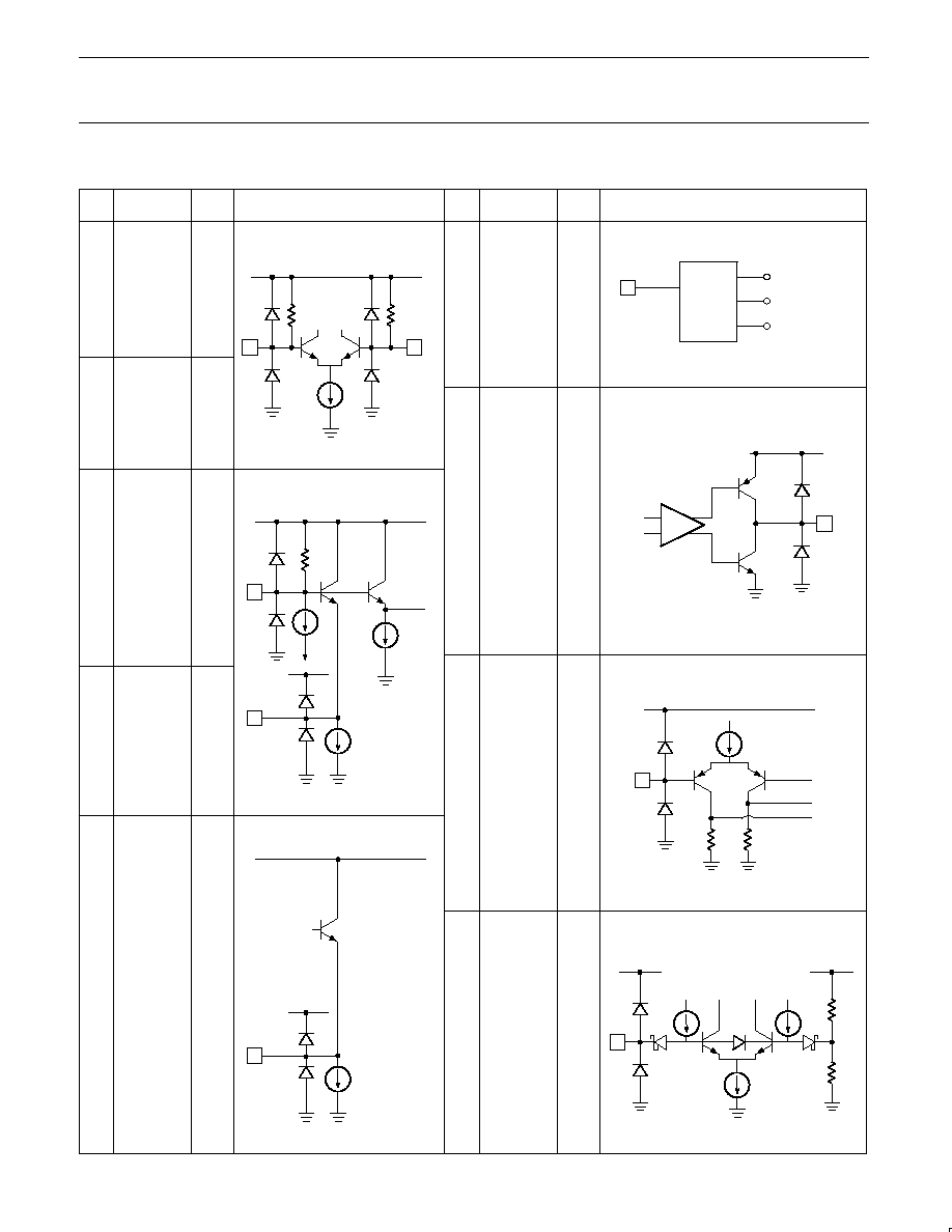
PIN FUNCTIONS
1
2.5k
2
2.5k
4
3
18k
MIX
150
µ
A
6
VREF
BANDGAP
8
+
VCC
--
7
VCC
+
--
9
R
R
PIN
No.
PIN
MNEMONIC
DC V
EQUIVALENT CIRCUIT
PIN
No.
PIN
MNEMONIC
DC V
EQUIVALENT CIRCUIT
1
RF IN
+1.40
8
RSSI
+0.20
FEEDBACK
2
RF
+1.40
7
RSSI
+0.20
OUT
BYPASS
3
OSC
+1.79
9
POWER
+2.00
DOWN
E
4
OSC
+2.56
B
6
V
CC
+3.00
5
150
µ
A
5
OSC
+1.79
BUFFER
Philips Semiconductors RF Communications Products
Product specification
SA637
Low-voltage digital IF receiver
October 27, 1993
8
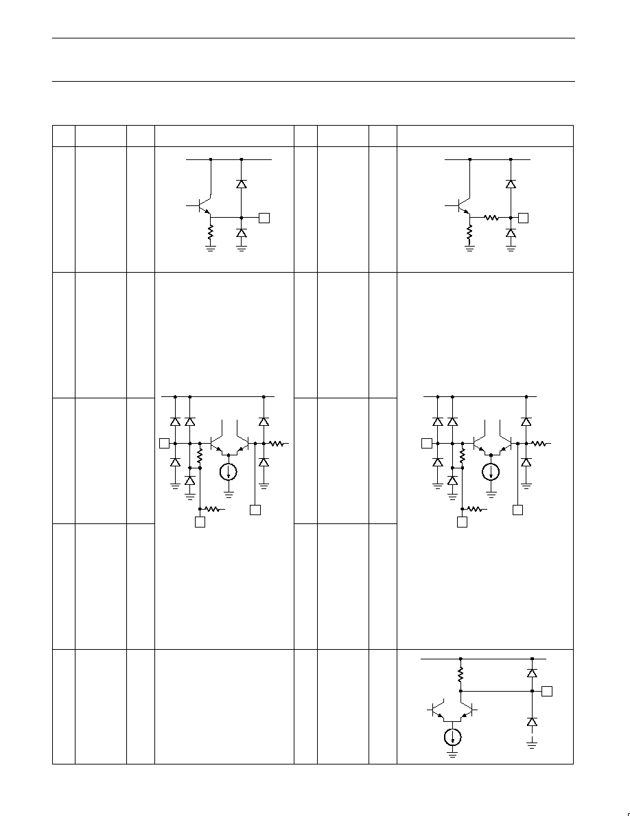
PIN FUNCTIONS (continued)
11
14
20
PIN
No.
PIN
MNEMONIC
DC V
EQUIVALENT CIRCUIT
PIN
No.
PIN
MNEMONIC
DC V
EQUIVALENT CIRCUIT
11
LIMITER
+1.25
16
IF
+1.28
AMP OUT
12
LIMITER
+1.28
17
IF AMP
+1.28
DECOUP
DECOUP
13
LIMITER
+1.28
18
IF
+1.28
AMP IN
COUPLING
14
LIMITER
+1.28
19
IF AMP
+1.28
DECOUP
IN
15
GND
0
20
MIXER
+2.03
OUT
OUT
8.8k
16
6.6k
1.31k
13
12
1.5k
50
µ
A
18
19
17
1.5k
50
µ
A
10
1.87k
Philips Semiconductors RF Communications Products
Product specification
SA637
Low-voltage digital IF receiver
October 27, 1993
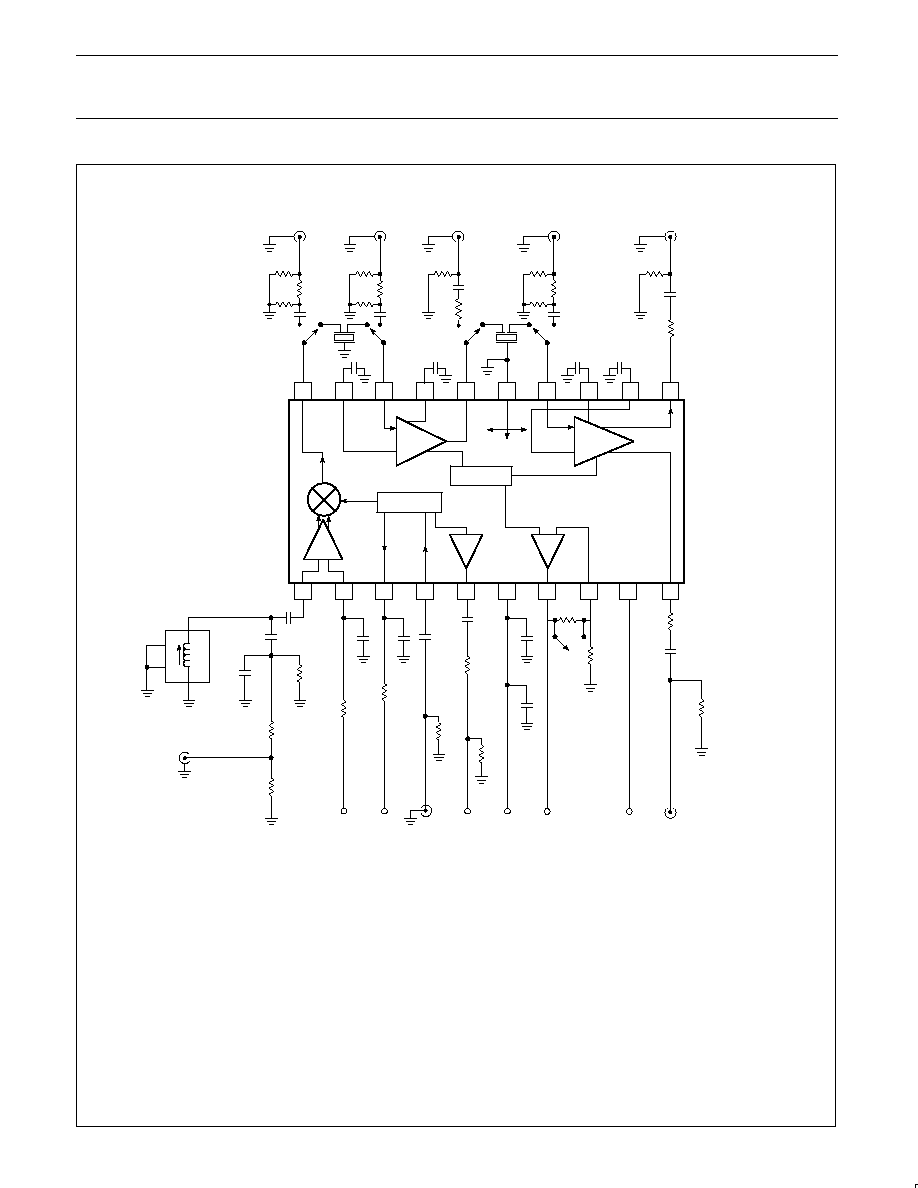
9
10
9
8
7
6
5
4
3
2
1
20
19
18
17
16
15
14
13
12
11
FAST RSSI
MIXER
RSSI BUFFER
PWD
C11
VCC
R49
R47
R48
R29
R28
R27
C20
C27
C29
C30
C31
C33
C32
FLT2
SW7
SW6
SW8
SW9
C26
C28
R31
FLT1
10nF
C1
C2
C3
C4
C5
C6
C11
C20
C21
C26
Automatic Test Circuit Component List
R38
R37
R33
R35
R34
R32
OSCILLATOR
LIMITER
+ ≠
+ ≠
RSSI FB
OSC
C21
R50
Figure 1. SA637 Automatic Test Circuit
PAD
IF
AMP
C12
C5
C4
100nF
10nF
91pF
620pF
100nF
100nF
100nF
100nF
100nF
C30
C31
C27
C28
C29
C32
C33
R1
R2
R3
100nF
100nF
100nF
100nF
100nF
100nF
R16
R17
R4
R13
R14
R20
R27
R28
R29
R31
49.9
10k
10k
100nF
249
60.4
60.4
PAD
PAD
PAD
PAD
10k
10k
1k
13.7k
1.68k
1k
49.9
R35
R38
R32
R33
R34
R39
R45
R47
R48
R49
49.9
13.7k
1.68k
49.9
49.9
1k
49.9
2.43k
49.9
39.2k
R50
R51
L2
1k
49.9
62nH
48dB
32.2dB
48dB
32.2dB
LIMITER
OUT (+)
LO
BUFF
R51
LIMITER
OUT (≠)
RSSI
OUT
LO
IN
RF
IN
R20
R16
C22
R17
R45
C6
R4
R14
R13
C1
C2
C3
R2
L2
R1
R3
R32 49.9
Philips Semiconductors RF Communications Products
Product specification
SA637
Low-voltage digital IF receiver
October 27, 1993
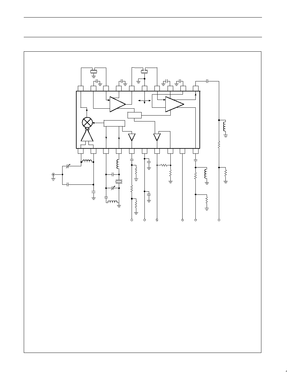
10
10
8
7
6
4
3
2
1
5
9
20
19
18
17
16
14
13
12
11
15
RSSI
MIXER
LO
OSC
OUT
C8
R1
C7
C2
C15
X1
L3
VCC
C14
C12
C1
L1
C5
C11
C6
FLT2
C3
C4
FLT1
5-30pF
5-30pF
10pF
1000pF
0.1
µ
F
68pF
1.0
µ
F
R2
R3
R4
R5
R6
R7
R8
R9
L2
L1
0
(short)
1k
OPEN
100
C1
C2
C5
C6
C7
C8
C9
C10
C12
C14
C15
RF
INPUT
LIMITER
OSCILLATOR
+ ≠
+ ≠
R2
R1
OPEN
L3
L4
L5
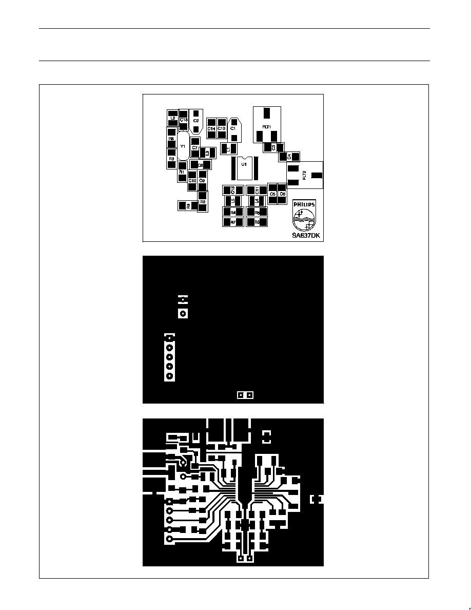
Figure 2. SA637 Application Circuit
FLT1
100
51
* NOTE: These components are optional and depend on user matching requirements.
IF
AMP
R3
R8
C9
C10
LIMITER
OUT(≠)
LIMITER
OUT(+)
POWER
DOWN
RSSI
R9
R4
R7
R6
L4
L5
C13
R5
BUFF
RSSI BUFF
RSSI FB
Component List
C3
C4
0.1
µ
F
0.1
µ
F
0.1
µ
F
0.1
µ
F
0.1
µ
F
C11 0.1
µ
F
C13 0.1
µ
F
0.1
µ
F
1.0k
2.0k
0.15
µ
H PM20-R15M
0.15
µ
H PM20-R15M
0.47
µ
H PM20-R47M
OPEN
OPEN
455kHz SFGCC 455BX-TC
FLT2
455kHz SFGCC 455BX-TC
X1
82.705MHz CTS XTAL 020-3249-042
Pads are provided on the demo board.
R2 and R9 set the RSSI buffer gain. For unity gain short R2 (Pin 7 to Pin 8)
and leave R9 open.
*
*
*
*
*
*
*
*
*
L2
Philips Semiconductors RF Communications Products
Product specification
SA637
Low-voltage digital IF receiver
October 27, 1993
11
DC VOLTMETER
RSSI
LIMITER
Figure 3. SA637 Application Circuit Test Set Up
SA637 DEMO BOARD
V
CC
= 3V
SPECTRUM
ANALYZER
OUTPUT
RF GENERATOR
83.16MHz
NOTES:
1. Carrier-to-Noise (C/N): Connect a spectrum analyzer to Pin 10 or 11; set your RF generator to 83.16MHz or 455kHz above your LO fre-
quency, modulation off; set the spectrum analyzer resolution bandwidth to 300Hz; and adjust your RF input level until the C/N = 26dB. Use
video averaging. Assure that LIMOUT(+) and LIMOUT(≠) are matched symetrically.
2. Ceramic filters: The ceramic filter can be SFGCC455BX-TC made by Murata which has 30kHz IF bandwidth.
3. Sensitivity: The measured typical sensitivity for 12dB SINAD should be 0.45
µ
V or -114dBm at the RF input.
4. Layout: The layout is very critical in the performance of the receiver. We highly recommend our demo board layout.
5. RSSI: The smallest RSSI voltage (i.e., when no RF input is present and the input is terminated) is a measure of the quality of the layout and
design. If the lowest RSSI voltage is 500mV or higher, it means the receiver is in regenerative mode. In that case, the receiver sensitivity
will be worse than expected.
6. Supply bypass and shielding: All of the inductors, the quad tank, and their shield must be grounded. A 0.1
µ
F bypass capacitor on the sup-
ply pin improves sensitivity.
Philips Semiconductors RF Communications Products
Product specification
SA637
Low-voltage digital IF receiver
October 27, 1993
12