 | –≠–ª–µ–∫—Ç—Ä–æ–Ω–Ω—ã–π –∫–æ–º–ø–æ–Ω–µ–Ω—Ç: SA7016 | –°–∫–∞—á–∞—Ç—å:  PDF PDF  ZIP ZIP |
Philips
Semiconductors
SA7016
1.3GHz low voltage fractional-N
synthesizer
Product specification
Supersedes data of 1999 Apr 20
1999 Nov 04
INTEGRATED CIRCUITS
Philips Semiconductors
Product specification
SA7016
1.3GHz low voltage fractional-N synthesizer
2
1999 Nov 04
853≠2160 22634
GENERAL DESCRIPTION
The SA7016 BICMOS device integrates programmable dividers,
charge pumps and a phase comparator to implement a
phase-locked loop. The device is designed to operate from 3 NiCd
cells, in pocket phones, with low current and nominal 3 V supplies.
The synthesizer operates at VCO input frequencies up to 1.3 GHz.
The synthesizer has fully programmable main and reference
dividers. All divider ratios are supplied via a 3-wire serial
programming bus.
Separate power and ground pins are provided to the analog and
digital circuits. The ground leads should be externally short-circuited
to prevent large currents flowing across the die and thus causing
damage. V
DDCP
must be greater than or equal to
V
DD
.
The charge pump current (gain) is set by an external resistance at
the R
SET
pin
.
Only passive loop filters could be used; the charge
pump operates within a wide voltage compliance range to provide a
wider tuning range.
FEATURES
∑
Low phase noise
∑
Low power
∑
Fully programmable main divider
∑
Internal fractional spurious compensation
∑
Hardware and software power down
∑
Split supply for V
DD
and V
DDCP
SR01505
1
2
3
4
5
6
7
8
9
10
11
12
13
14
15
16
LOCK
TEST
V
DD
GND
RFin+
RFin≠
GND
CP
PHP
PON
STROBE
DATA
CLOCK
REFin+
REFin≠
R
SET
V
DDCP
Figure 1.
Pin Configuration
APPLICATIONS
∑
350≠1300 MHz wireless equipment
∑
Cellular phones
∑
Portable battery-powered radio equipment.
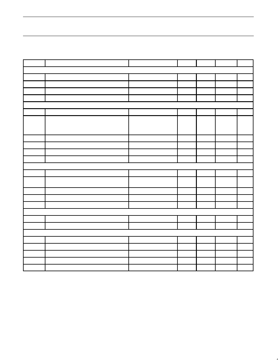
QUICK REFERENCE DATA
SYMBOL
PARAMETER
CONDITIONS
MIN.
TYP.
MAX.
UNIT
V
DD
Supply voltage
2.7
≠
5.5
V
V
DDCP
Analog supply voltage
V
DDCP
V
DD
2.7
≠
5.5
V
I
DDCP
+I
DD
Total supply current
≠
6.2
7.3
mA
I
DDCP
+I
DD
Total supply current in power-down mode
≠
1
≠
µ
A
f
VCO
Input frequency
350
≠
1300
MHz
f
REF
Crystal reference input frequency
5
≠
40
MHz
f
PC
Maximum phase comparator frequency
≠
4
MHz
T
amb
Operating ambient temperature
≠40
≠
+85
∞
C
ORDERING INFORMATION
TYPE NUMBER
PACKAGE
TYPE NUMBER
NAME
DESCRIPTION
VERSION
SA7016DH
TSSOP16
Plastic thin shrink small outline package; 16 leads; body width 4.4 mm
SOT403≠1
Philips Semiconductors
Product specification
SA7016
1.3GHz low voltage fractional-N synthesizer
1999 Nov 04
3
SR01506
CLOCK
DATA
STROBE
RFin+
RFin≠
REF
in+
REF
in≠
TEST
LOAD SIGNALS
ADDRESS DECODER
2≠BIT SHIFT
REGISTER
22≠BIT SHIFT
REGISTER
CONTROL
LATCH
LATCH
MAIN DIVIDER
REFERENCE
DIVIDER
LATCH
AMP
11
12
6
5
15
14
13
2
PHASE
DETECTOR
COMP
PUMP
BIAS
PUMP
CURRENT
SETTING
GND
4
7
3
GND
CP
V
DD
R
SET
V
DDCP
PHP
LOCK
10
9
8
1
PON
16
Figure 2.
Block Diagram
PINNING
SYMBOL
PIN
DESCRIPTION
LOCK
1
Lock detect output
TEST
2
Test (should be either grounded or
connected to V
DD)
V
DD
3
Digital supply
GND
4
Digital ground
RFin+
5
RF input to main divider
RFin≠
6
RF input to main divider
GND
CP
7
Charge pump ground
PHP
8
Main normal chargepump
V
DDCP
9
Charge pump supply voltage
R
SET
10
External resistor from this pin to ground
sets the chargepump current
REFin≠
11
Reference input
REFin+
12
Reference input
CLOCK
13
Programming bus clock input
DATA
14
Programming bus data input
STROBE
15
Programming bus enable input
PON
16
Power down control
Philips Semiconductors
Product specification
SA7016
1.3GHz low voltage fractional-N synthesizer
1999 Nov 04
4
LIMITING VALUES
In accordance with the Absolute Maximum Rating System (IEC 134).
SYMBOL
PARAMETER
MIN.
MAX.
UNIT
V
DD
Digital supply voltage
≠0.3
+5.5
V
V
DDCP
Analog supply voltage
≠0.3
+5.5
V
V
DDCP
≠V
DD
Difference in voltage between V
DDCP and
V
DD
(V
DDCP
V
DD
)
≠0.3
+2.8
V
V
n
Voltage at pins 1, 2, 5, 6, 11 to 16
≠0.3
V
DD
+ 0.3
V
V
1
Voltage at pin 8, 9
≠0.3
V
DDCP
+ 0.3
V
V
GND
Difference in voltage between GND
CP
and GND (these pins should
be connected together)
≠0.3
+0.3
V
T
stg
Storage temperature
≠55
+125
_
C
T
amb
Operating ambient temperature
≠40
+85
_
C
T
j
Maximum junction temperature
150
_
C
Handling
Inputs and outputs are protected against electrostatic discharge in
normal handling. However, to be totally safe, it is desirable to take
normal precautions appropriate to handling MOS devices.
THERMAL CHARACTERISTICS
SYMBOL
PARAMETER
VALUE
UNIT
R
th j≠a
Thermal resistance from junction to ambient in free air
120
K/W
Philips Semiconductors
Product specification
SA7016
1.3GHz low voltage fractional-N synthesizer
1999 Nov 04
5
CHARACTERISTICS
V
DDCP
= V
DD
= +3.0V,
T
amb
= +25
∞
C;
unless otherwise specified.
SYMBOL
PARAMETER
CONDITIONS
MIN.
TYP.
MAX.
UNIT
Supply; pins 3, 9
V
DD
Digital supply voltage
2.7
≠
5.5
V
V
DDCP
Analog supply voltage
V
DDCP
= V
DD
2.7
≠
5.5
V
I
DDTotal
Synthesizer operational total supply current
V
DD
= +3.0V
≠
6.2
7.3
mA
I
Standby
Total supply current in power-down mode
logic levels 0 or V
DD
≠
1
TBD
µ
A
RFin main divider input; pins 5, 6
f
VCO
VCO input frequency
350
≠
1300
MHz
V
RFin(rms)
AC-coupled input signal level
R
in
(external) = R
s
= 50
;
single-ended drive;
max. limit is indicative
@ 500 to 1300 MHz
≠18
≠
0
dBm
Z
IRFin
Input impedance (real part)
f
VCO
= 1.2 GHz
≠
625
≠
C
IRFin
Typical pin input capacitance
f
VCO
= 1.2 GHz
≠
1.0
≠
pF
N
main
Main divider ratio
512
≠
65535
f
PCmax
Maximum loop comparison frequency
indicative, not tested
≠
≠
4
MHz
Reference divider input; pins 11, 12
f
REFin
Input frequency range from TCXO
5
≠
40
MHz
VRFin
AC-coupled input signal level
single-ended drive;
max. limit is indicative
360
≠
1300
mV
PP
Z
REFin
Input impedance (real part)
f
REF
= 20 MHz
≠
10
≠
k
C
REFin
Typical pin input capacitance
f
REF
= 20 MHz
≠
1.0
≠
pF
R
REF
Reference division ratio
4
≠
1023
Charge pump current setting resistor input; pin 10
R
SET
External resistor from pin to ground
6
7.5
15
k
V
SET
Regulated voltage at pin
R
SET
=7.5 k
≠
1.25
≠
V
Charge pump outputs (including fractional compensation pump); pin 8; R
SET
=7.5k
, FC=80
I
CP
Charge pump current ratio to I
SET
1
Current gain I
PH
/I
SET
≠15
+15
%
I
MATCH
Sink-to-source current matching
V
PH
=1/2 V
DDCP
.
≠10
+10
%
I
ZOUT
Output current variation versus V
PH
2
V
PH
in compliance range
≠10
+10
%
I
LPH
Charge pump off leakage current
V
PH
=1/2 V
CC
≠10
+10
nA
V
PH
Charge pump voltage compliance
0.7
≠
V
DDCP
≠0.8
V
Philips Semiconductors
Product specification
SA7016
1.3GHz low voltage fractional-N synthesizer
1999 Nov 04
6
SYMBOL
UNIT
MAX.
TYP.
MIN.
CONDITIONS
PARAMETER
Phase noise (R
SET
= 7.5 k
, CP=00)
L
Synthesizer's contribution to close-in phase noise
of 900 MHz RF signal at 1 kHz offset.
GSM
f
REF
= 13MHz, TCXO,
f
COMP
= 1MHz
indicative, not tested
≠
≠90
≠
dBc/Hz
L
(f)
Synthesizer's contribution to close-in phase noise
of 800 MHz RF signal at 1 kHz offset.
TDMA
f
REF
= 19.44MHz, TCXO,
f
COMP
= 240kHz
indicative, not tested
≠
≠85
≠
dBc/Hz
Interface logic input signal levels; pins 13, 14, 15, 16
V
IH
HIGH level input voltage
0.7*V
DD
≠
V
DD
+0.3
V
V
IL
LOW level input voltage
≠0.3
≠
0.3*V
DD
V
I
LEAK
Input leakage current
logic 1 or logic 0
≠0.5
≠
+0.5
µ
A
Lock detect output signal (in push/pull mode); pin 1
V
OL
LOW level output voltage
I
sink
=2mA
≠
≠
0.4
V
V
OH
HIGH level output voltage
I
source
=≠2mA
V
DD
≠0.4
≠
≠
V
NOTES:
1. I
SET =
V
SET
R
SET
bias current for charge pumps.
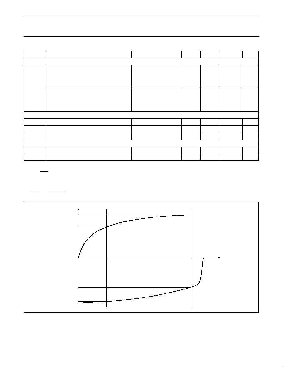
2. The relative output current variation is defined as:
D
I
OUT
I
OUT
+
2
.
(I
2
≠I
1
)
I(I
2
)
I
1
)I
; with V
1
+
0.7V, V
2
+
V
DDCP
≠0.8V (See Figure 3.)
I2
I1
I2
I1
V1
V2
CURRENT
V
PH
SR00602
I
ZOUT
Figure 3.
Relative Output Current Variation
Philips Semiconductors
Product specification
SA7016
1.3GHz low voltage fractional-N synthesizer
1999 Nov 04
7
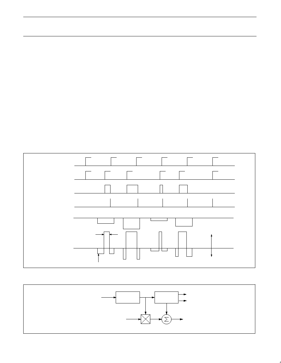
FUNCTIONAL DESCRIPTION
Main Fractional-N divider
The RFin inputs drive a pre-amplifier to provide the clock to the first
divider stage. For single ended operation, the signal should be fed to
one of the inputs while the other one is AC grounded. The
pre-amplifier has a high input impedance, dominated by pin and pad
capacitance. The circuit operates with signal levels from ≠18 dBm to
0 dBm, and at frequencies as high as 1.3 GHz. The divider consists
of a fully programmable bipolar prescaler followed by a CMOS
counter. Total divide ratios range from 512 to 65536.
At the completion of a main divider cycle, a main divider output
pulse is generated which will drive the main phase comparator. Also,
the fractional accumulator is incremented by the value of NF. The
accumulator works with modulo Q set by FMOD. When the
accumulator overflows, the overall division ratio N will be increased
by 1 to N + 1, the average division ratio over Q main divider cycles
(either 5 or 8) will be
Nfrac
+
N
)
NF
Q
The output of the main divider will be modulated with a fractional
phase ripple. The phase ripple is proportional to the contents of the
fractional accumulator and is nulled by the fractional compensation
charge pump.
The reloading of a new main divider ratio is synchronized to the
state of the main divider to avoid introducing a phase disturbance.
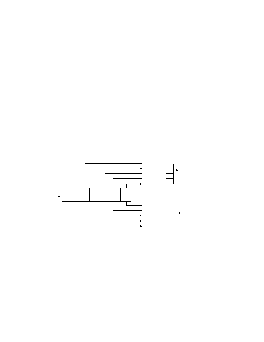
Reference divider
The reference divider consists of a divider with programmable
values between 4 and 1023 followed by a three bit binary counter.
The 3 bit SM (SA) register (see Figure 4) determines which of the 5
output pulses are selected as the main (auxiliary) phase detector
input.
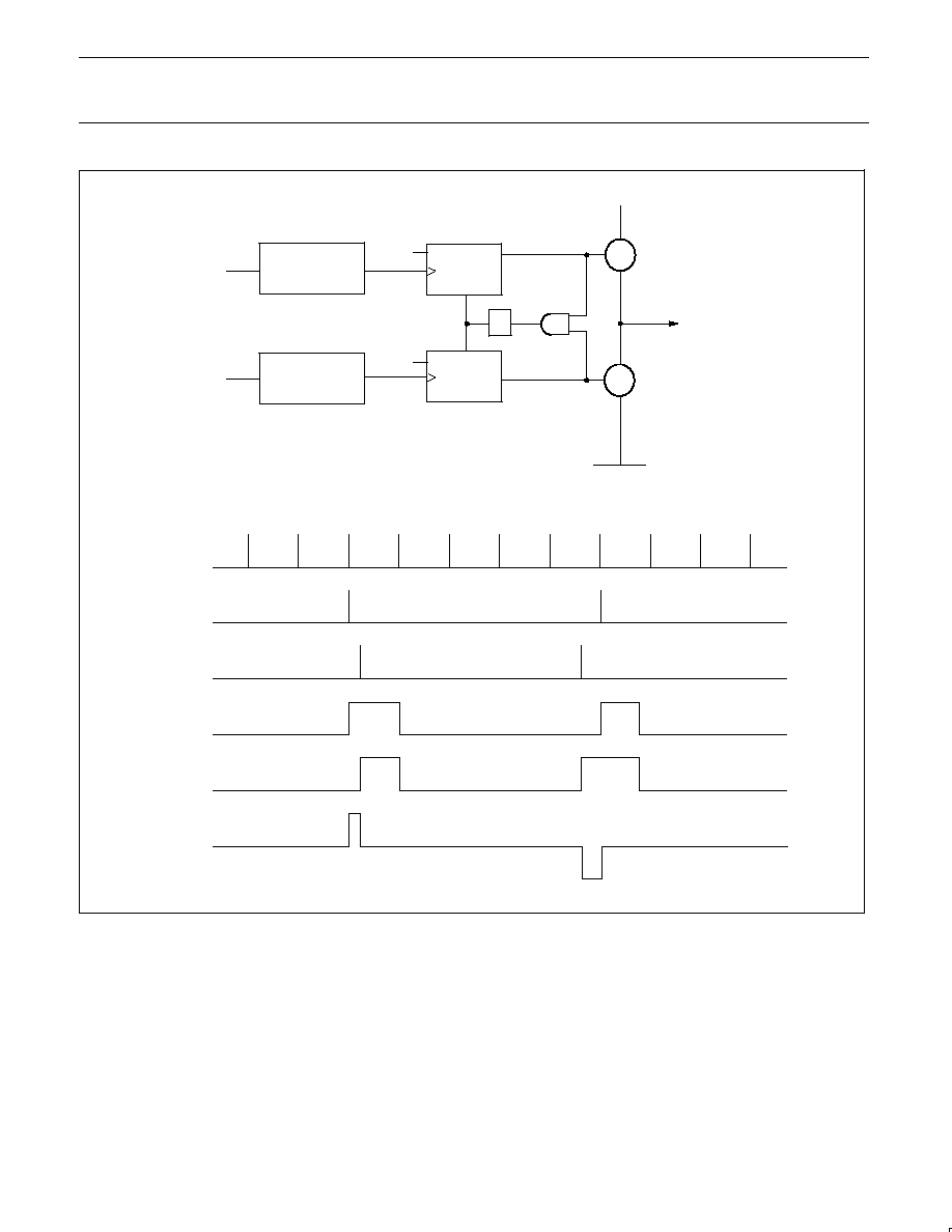
Phase detector (see Figure 5)
The reference and main (aux) divider outputs are connected to a
phase/frequency detector that controls the charge pump. The pump
current is set by an external resistor in conjunction with control bits
CP0 and CP1 in the C-word (see Charge Pump table). The dead
zone (caused by finite time taken to switch the current sources on or
off) is cancelled by forcing the pumps ON for a minimum time at
every cycle (backlash time) providing improved linearity.
SR01415
DIVIDE BY R
/2
/2
/2
/2
REFERENCE
INPUT
SM="000"
SM="001"
SM="010"
SM="011"
SM="100"
SA="100"
SA="011"
SA="010"
SA="001"
SA="000"
TO
MAIN
PHASE
DETECTOR
TO
AUXILIARY
PHASE
DETECTOR
Figure 4.
Reference Divider
Philips Semiconductors
Product specification
SA7016
1.3GHz low voltage fractional-N synthesizer
1999 Nov 04
8
SR02103
R
X
P
N
REF DIVIDER
AUX/MAIN
DIVIDER
D
Q
CLK
"1"
R
D
R
CLK
"1"
X
Q
N
P
V
CC
I
PH
GND
P≠TYPE
CHARGE PUMP
N≠TYPE
CHARGE PUMP
R
f
REF
f
REF
I
PH
Figure 5.
Phase Detector Structure with Timing
Philips Semiconductors
Product specification
SA7016
1.3GHz low voltage fractional-N synthesizer
1999 Nov 04
9
Main Output Charge Pumps and Fractional
Compensation Currents (see Figure 6)
The main charge pumps on pins PHP and PHI are driven by the
main phase detector and the charge pump current values are
determined by the current at pin R
SET
in conjunction with bits CP0,
CP1 in the B-word (see table of charge pump ratios). The fractional
compensation is derived from the current at R
SET
, the contents of
the fractional accumulator FRD and by the program value of the
FDAC. The timing for the fractional compensation is derived from
the main divider. The main charge pumps will enter speed up mode
after the A-word is set and strobe goes High. When strobe goes
Low, charge pump will exit speed up mode.
Principle of Fractional Compensation
The fractional compensation is designed into the circuit as a means
of reducing or eliminating fractional spurs that are caused by the
fractional phase ripple of the main divider. If I
COMP
is the
compensation current and I
PUMP
is the pump current, then for each
charge pump:
I
PUMP_TOTAL
= I
PUMP
+ I
COMP
.
The compensation is done by sourcing a small current, I
COMP
, see
Figure 7, that is proportional to the fractional error phase. For proper
fractional compensation, the area of the fractional compensation
current pulse must be equal to the area of the fractional charge
pump ripple. The width of the fractional compensation pulse is fixed
to 128 VCO cycles, the amplitude is proportional to the fractional
accumulator value and is adjusted by FDAC values (bits FC7≠0 in
the B-word). The fractional compensation current is derived from the
main charge pump in that it follows all the current scaling through
external resistor setting, R
SET
, programming or speed-up operation.
For a given charge pump,
I
COMP
= ( I
PUMP
/ 128 ) * ( FDAC / 5*128) * FRD
FRD is the fractional accumulator value.
The target values for FDAC are: 128 for FMOD = 1 (modulo 5) and
80 for FMOD = 0 (modulo 8).
SR01416
REFERENCE R
MAIN M
DIVIDE RATIO
DETECTOR
OUTPUT
ACCUMULATOR
FRACTIONAL
COMPENSATION
CURRENT
OUTPUT ON
PUMP
N
N
N+1
N
N+1
2
4
1
3
0
PULSE
WIDTH
MODULATION
PULSE LEVEL
MODULATION
mA
µ
A
NOTE: For a proper fractional compensation, the area of the fractional compensation current pulse must be equal to the area of the charge pump ripple output.
Figure 6.
Waveforms for NF = 2 Modulo 5
fraction =
2
/
5
SR01682
f
RF
1930.140 MHz
MAIN DIVIDER
N = 8042
FRACTIONAL
ACCUMULATOR
f
REF
240 kHz
240.016 kHz
I
COMP
I
PUMP
LOOP FILTER
& VCO
FMOD
NF
Figure 7.
Current Injection Concept

Philips Semiconductors
Product specification
SA7016
1.3GHz low voltage fractional-N synthesizer
1999 Nov 04
10
Charge pump currents
CP0
I
PHP
I
PHP≠SU
0
3xI
SET
15xl
SET
1
1xl
SET
5xl
SET
NOTES:
1. I
SET
=V
SET
/R
SET
: bias current for charge pumps.
2. I
PHP≠SU
is the total current at pin PHP during speed up condition.
Lock Detect
The output LOCK maintains a logic `1' when the auxiliary phase
detector ANDed with the main phase detector indicates a lock
condition. The lock condition for the main and auxiliary synthesizers
is defined as a phase difference of less than
"
1 period of the
frequency at the input REFin+, ≠. One counter can fulfill the lock
condition when the other counter is powered down. Out of lock (logic
`0') is indicated when both counters are powered down.
Power-down mode
The power-down signal can be either hardware (PON) or software
(PD). The PON signal is exclusively ORed with the PD bits in
B-word. If PON = 0, then the part is powered up when PD = 1. PON
can be used to invert the polarity of the software bit PD. When the
synthesizer is reactivated after power-down, the main and reference
dividers are synchronized to avoid possibility of random phase
errors on power-up.
Philips Semiconductors
Product specification
SA7016
1.3GHz low voltage fractional-N synthesizer
1999 Nov 04
11
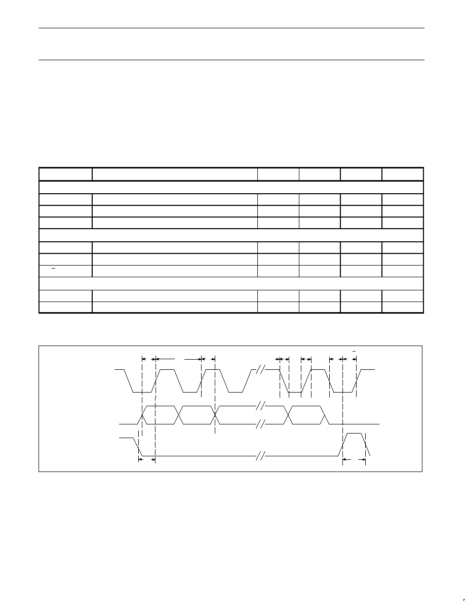
Serial programming bus
The serial input is a 3-wire input (CLOCK, STROBE, DATA) to
program all counter divide ratios, fractional compensation DAC,
selection and enable bits. The programming data is structured into
24 bit words; each word includes 2 or 3 address bits. Figure 8
shows the timing diagram of the serial input. When the STROBE
goes active HIGH, the clock is disabled and the data in the shift
register remains unchanged. Depending on the address bits, the
data is latched into different working registers or temporary
registers. In order to fully program the synthesizer, 3 words must be
sent: C, B, and A. Table 1 shows the format and the contents of
each word. The D word is normally used for testing purposes. When
sending the B-word, data bits FC7≠0 for the fractional compensation
DAC are not loaded immediately. Instead they are stored in
temporary registers. Only when the A-word is loaded, these
temporary registers are loaded together with the main divider ratio.
Serial bus timing characteristics. See Figure 8.
V
DD
= V
DDCP
=+3.0V; T
amb
= +25
∞
C unless otherwise specified.
SYMBOL
PARAMETER
MIN.
TYP.
MAX.
UNIT
Serial programming clock; CLK
t
r
Input rise time
≠
10
40
ns
t
f
Input fall time
≠
10
40
ns
T
cy
Clock period
100
≠
≠
ns
Enable programming; STROBE
t
START
Delay to rising clock edge
40
≠
≠
ns
t
W
Minimum inactive pulse width
1/f
COMP
≠
≠
ns
t
SU;E
Enable set-up time to next clock edge
20
≠
≠
ns
Register serial input data; DATA
t
SU;DAT
Input data to clock set-up time
20
≠
≠
ns
t
HD;DAT
Input data to clock hold time
20
≠
≠
ns
Application information
SR01417
CLK
DATA
STROBE
ADDRESS
LSB
t
SU;DAT
t
HD;DAT
t
r
t
w
t
f
t
SU;E
t
START
T
cy
MSB
Figure 8.
Serial Bus Timing Diagram
Philips Semiconductors
Product specification
SA7016
1.3GHz low voltage fractional-N synthesizer
1999 Nov 04
12
Data format
Table 1. Format of programmed data
LAST IN
MSB
SERIAL PROGRAMMING FORMAT
FIRST IN LSB
p23
p22
p21
p20
../..
../..
p1
p0
Table 2. A word, length 24 bits
LAST IN
MSB
LSB
FIRST IN
Address
fmod
Fractional-N
Main Divider ratio
Spare
0
0
FM
NF2
NF1
NF0
N15
N14
N13
N12
N11
N10
N9
N8
N7
N6
N5
N4
N3
N2
N1
N0
SP1
SP2
Default:
0
0
1
0
0
0
1
0
0
0
1
0
0
0
1
1
0
0
0
0
0
0
A word select
Fixed to 00.
Fractional Modulus select
FM 0 = modulo 8, 1 = modulo 5.
Fractional-N Increment
NF2..0 Fractional N Increment values 000 to 111.
N-Divider
N0..N15, Main divider values 512 to 65535 allowed for divider ratio.
Table 3. B word, length 24 bits
Address
REFERENCE DIVIDER
LOCK
PD
CP
FRACTIONAL COMPENSATION DAC
SPARE
0
1
R9
R8
R7
R6
R5
R4
R3
R2
R1
R0
LO
MAIN
CP0
FC7
FC6
FC5
FC4
FC3
FC2
FC1
FC0
SP3
Default:
0
0
0
1
0
1
0
0
0
1
0
0
0
0
1
0
1
0
0
0
0
0
B word select
Fixed to 01
R-Divider
R0..R9, Reference divider values 4 to 1023 allowed for divider ration.
Charge pump current
Ratio
CP0: Charge pump current ratio, see table of charge pump currents.
Lock detect output
L0
0
Main lock detect signal present at the LOCK pin (push/pull).
1
Main lock detect signal present at the LOCK pin (open drain).
When main loop is in power down mode, the lock indicator is low.
Power down
Main = 1: power to main divider, reference divider, main charge pumps, Main = 0 to power down.
Fractional Compensation
FC7..0 Fractional Compensation charge pump current DAC, values 0 to 255.
Table 4. D word, length 24 bits
Address
SYNTHESIZER TEST
BITS
SYNTHESIZER TEST BITS
1
1
0
≠
≠
≠
≠
≠
Tspu
≠
≠
≠
≠
≠
≠
≠
≠
≠
≠
≠
≠
≠
≠
≠
Default:
0
0
0
0
0
0
0
0
0
0
0
0
0
0
0
0
0
0
0
0
0
Tspu: Speed up = 1
Forces the main charge pumps in speed-up mode all the time.
NOTE: All test bits must be set to 0 for normal operation.
Philips Semiconductors
Product specification
SA7016
1.3GHz low voltage fractional-N synthesizer
1999 Nov 04
13
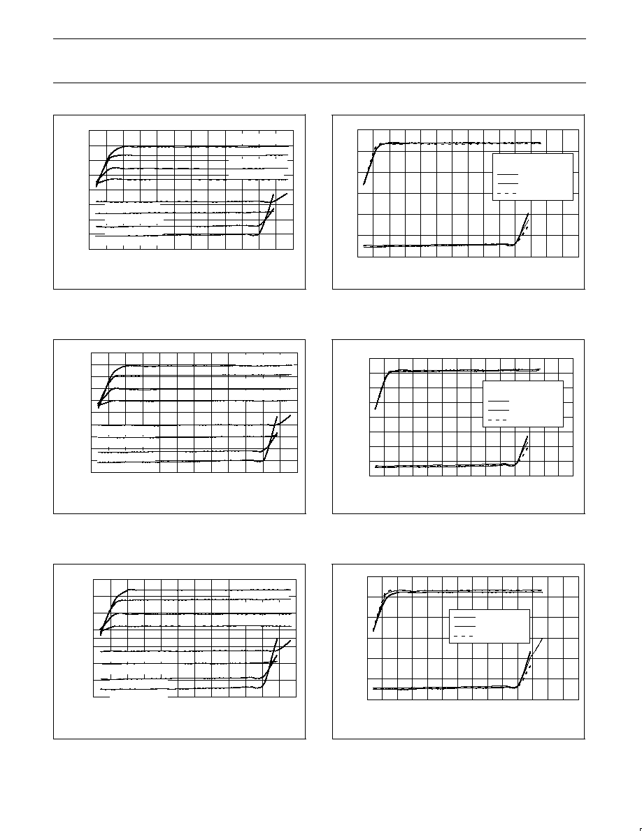
SR01911
0
0.25
0.5
0.75
1
1.25
1.5
1.75
2
2.25
2.5
2.75
3
800
600
400
200
0
≠200
≠400
≠600
≠800
Icp (uA)
COMPLIANCE VOLTAGE (V)
I
SET
= 206.67
m
A
I
SET
= 165.33
m
A
I
SET
= 103.33
m
A
I
SET
= 51.67
m
A
I
SET
= 51.67
m
A
I
SET
= 103.33
m
A
I
SET
= 165.33
m
A
I
SET
= 206.67
m
A
Figure 9.
Php Charge Pump Output vs. I
SET
(CP = 0, TEMP = 25
_
C)
SR01912
600
400
200
0
≠200
≠400
≠600
0
0.25
0.5 0.75
1
1.25 1.5 1.75
2
2.25 2.5 2.75
3
3.25 3.5
COMPLIANCE VOLTAGE (V)
Icp (uA)
TEMP = 85
∞
C
TEMP = 25
∞
C
TEMP = ≠40
∞
C
V
dd
= 3.0 V
I
SET
= 165.33
µ
A
Figure 10.
Php Charge Pump Output vs. Temperature
(CP = 0; V
DD
= 3.0 V; I
SET
= 165.33
m
A)
SR01913
Icp (uA)
≠250
250
200
150
100
50
0
≠50
≠100
≠150
≠200
0
0.25
0.5
0.75
1
1.25
1.5
1.75
2
2.25
2.5
2.75
3
COMPLIANCE VOLTAGE (V)
I
SET
= 206.67
m
A
I
SET
= 165.33
m
A
I
SET
= 103.33
m
A
I
SET
= 51.67
m
A
I
SET
= 51.67
m
A
I
SET
= 103.33
m
A
I
SET
= 165.33
m
A
I
SET
= 206.67
m
A
Figure 11.
Php Charge Pump Output vs. I
SET
(CP = 1; TEMP = 25
_
C)
SR01914
≠200
Icp (uA)
200
150
100
50
0
≠50
≠100
≠150
0
0.25 0.5 0.75
1
1.25 1.5 1.75
2
2.25 2.5 2.75
3
3.25 3.5
COMPLIANCE VOLTAGE (V)
TEMP = 85
∞
C
TEMP = 25
∞
C
TEMP = ≠40
∞
C
V
dd
= 3.0 V
I
SET
= 165.33
µ
A
Figure 12.
Php Charge Pump Output vs. Temperature
(CP = 1; V
DD
= 3.0 V; I
SET
= 165.33
m
A)
SR01915
≠3500
Icp (uA)
≠2500
≠1500
≠500
0
500
1500
2500
3500
0
0.25
0.5
0.75
1
1.25
1.5
1.75
2
2.25
2.5
2.75
3
COMPLIANCE VOLTAGE (V)
I
SET
= 206.67
m
A
I
SET
= 165.33
m
A
I
SET
= 103.33
m
A
I
SET
= 51.67
m
A
I
SET
= 51.67
m
A
I
SET
= 103.33
m
A
I
SET
= 165.33
m
A
I
SET
= 206.67
m
A
Figure 13.
Php≠su Charge Pump Output vs. I
SET
(CP = 0; TEMP = 25
_
C)
SR01916
3000
Icp (uA)
2000
1000
0
≠1000
≠2000
≠3000
0
0.25 0.5 0.75
1
1.25 1.5 1.75
2
2.25 2.5 2.75
3
3.25 3.5
COMPLIANCE VOLTAGE (V)
TEMP = 85
_
C
TEMP = 25
_
C
TEMP = ≠40
_
C
Figure 14.
Php≠su Charge Pump Output vs. Temperature
(CP = 0; V
DD
= 3.0 V; I
SET
= 165.33
m
A)

Philips Semiconductors
Product specification
SA7016
1.3GHz low voltage fractional-N synthesizer
1999 Nov 04
14
I
SET
= 165.33
m
A
I
SET
= 206.67
m
A
SR01917
Icp (uA)
I
SET
= 206.67
m
A
I
SET
= 165.33
m
A
I
SET
= 103.33
m
A
I
SET
= 51.67
m
A
I
SET
= 51.67
m
A
I
SET
= 103.33
m
A
1500
1000
500
0
≠500
≠1000
≠1500
0
0.25
0.5 0.75
1
1.5
1.25
1.75
2
2.25
2.5 2.75
3
COMPLIANCE VOLTAGE (V)
Figure 15.
Php≠su Charge Pump Output vs. I
SET
(CP = 1; TEMP = 25
_
C)
SR01918
≠1000
Icp (uA)
1000
800
600
400
200
0
≠200
≠400
≠600
≠800
0 0.25 0.5 0.75 1 1.25 1.5 1.75
2 2.25 2.5 2.75 3
3.25 3.5
COMPLIANCE VOLTAGE (V)
TEMP = 85
_
C
TEMP = 25
_
C
TEMP = ≠40
_
C
Figure 16.
Php≠su Charge Pump Output vs. Temperature
(CP = 1; V
DD
= 3.0 V; I
SET
= 165.33
m
A)
SR01929
≠40
MINIMUM
SIGNAL
INPUT
LEVEL
(dBm)
V
DD
= 5.50 V
V
DD
= 3.75 V
V
DD
= 3.00 V
V
DD
= 2.70 V
≠35
≠30
≠25
≠20
≠15
≠10
≠5
0
0
200
400
600
800
1000
1200
1400
1600
FREQUENCY (MHz)
≠45
≠50
≠55
≠60
1800
2000
Figure 17.
Main Divider Input Sensitivity vs. Frequency and
Supply Voltage (TEMP = 25
_
C)
SR01930
≠45
MINIMUM
SIGNAL
INPUT
LEVEL
(dBm)
+85
_
C
+25
_
C
≠40
_
C
≠40
≠35
≠30
≠25
≠20
≠15
≠10
0
≠5
0
200
400
600
800
1000
1200
1400
1600
1800
FREQUENCY (MHz)
≠50
2000
Figure 18.
Main Divider Input Sensitivity vs. Frequency and
Temperature (V
DD
= 3.00 V)
SR01921
MINIMUM
SIGNAL
POWER LEVEL
(dBm)
≠55
≠50
≠45
≠40
≠35
≠30
≠25
≠20
≠15
≠10
≠5
0
0
5
10
15
20
25
30
35
40
45
50
55
60
65
70
FREQUENCY (MHz)
V
DD
= 5.00 V
V
DD
= 3.75 V
V
DD
= 3.00 V
V
DD
= 2.70 V
Figure 19.
Reference Divider Input Sensitivity vs. Frequency
and Supply Voltage (TEMP = 25
_
C)
SR01922
≠55
MINIMUM
SIGNAL
POWER LEVEL
(dBm)
0
≠5
≠10
≠15
≠20
≠25
≠30
≠35
≠40
≠45
≠50
0
5
10
15
20
25
30
35
40
45
50
55
60
65
70
FREQUENCY (MHz)
TEMP = +85
_
C
TEMP = +25
_
C
TEMP = ≠40
_
C
Figure 20.
Reference Divider Input Sensitivity vs. Frequency
and Temperature (V
DD
= 3.00 V)
Philips Semiconductors
Product specification
SA7016
1.3GHz low voltage fractional-N synthesizer
1999 Nov 04
15
SR01931
8
I T
O
T
A
L
(mA)
8.5
7.5
7
6.5
6
5.5
2.5
3
3.5
4
4.5
5
5.5
6
TEMP = +85
_
C
TEMP = +25
_
C
TEMP = ≠40
_
C
SUPPLY VOLTAGE (V)
Figure 21.
Current Supply Over V
DD
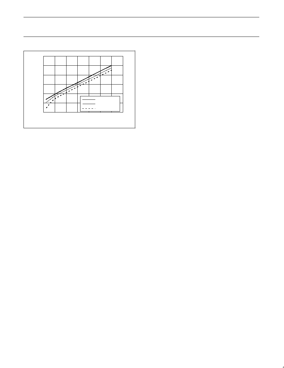
1.3GHz low voltage fractional-N frequency
synthesizer
Philips Semiconductors
Product specification
SA7016
1999 Nov 04
16
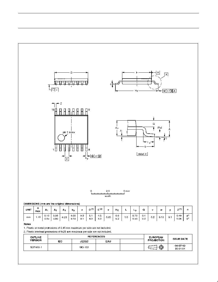
TSSOP16:
plastic thin shrink small outline package; 16 leads; body width 4.4 mm
SOT403-1

1.3GHz low voltage fractional-N frequency
synthesizer
Philips Semiconductors
Product specification
SA7016
1999 Nov 04
17
NOTES
1.3GHz low voltage fractional-N frequency
synthesizer
Philips Semiconductors
Product specification
SA7016
1999 Nov 04
18
Definitions
Short-form specification -- The data in a short-form specification is extracted from a full data sheet with the same type number and title. For
detailed information see the relevant data sheet or data handbook.
Limiting values definition -- Limiting values given are in accordance with the Absolute Maximum Rating System (IEC 134). Stress above one
or more of the limiting values may cause permanent damage to the device. These are stress ratings only and operation of the device at these or
at any other conditions above those given in the Characteristics sections of the specification is not implied. Exposure to limiting values for extended
periods may affect device reliability.
Application information -- Applications that are described herein for any of these products are for illustrative purposes only. Philips
Semiconductors make no representation or warranty that such applications will be suitable for the specified use without further testing or
modification.
Disclaimers
Life support -- These products are not designed for use in life support appliances, devices or systems where malfunction of these products can
reasonably be expected to result in personal injury. Philips Semiconductors customers using or selling these products for use in such applications
do so at their own risk and agree to fully indemnify Philips Semiconductors for any damages resulting from such application.
Right to make changes -- Philips Semiconductors reserves the right to make changes, without notice, in the products, including circuits, standard
cells, and/or software, described or contained herein in order to improve design and/or performance. Philips Semiconductors assumes no
responsibility or liability for the use of any of these products, conveys no license or title under any patent, copyright, or mask work right to these
products, and makes no representations or warranties that these products are free from patent, copyright, or mask work right infringement, unless
otherwise specified.
Philips Semiconductors
811 East Arques Avenue
P.O. Box 3409
Sunnyvale, California 94088≠3409
Telephone 800-234-7381
©
Copyright Philips Electronics North America Corporation 1999
All rights reserved. Printed in U.S.A.
Date of release: 11-99
Document order number:
9397 750 06565
Philips
Semiconductors
Data sheet
status
Objective
specification
Preliminary
specification
Product
specification
Product
status
Development
Qualification
Production
Definition
[1]
This data sheet contains the design target or goal specifications for product development.
Specification may change in any manner without notice.
This data sheet contains preliminary data, and supplementary data will be published at a later date.
Philips Semiconductors reserves the right to make chages at any time without notice in order to
improve design and supply the best possible product.
This data sheet contains final specifications. Philips Semiconductors reserves the right to make
changes at any time without notice in order to improve design and supply the best possible product.
Data sheet status
[1]
Please consult the most recently issued datasheet before initiating or completing a design.