 | –≠–ª–µ–∫—Ç—Ä–æ–Ω–Ω—ã–π –∫–æ–º–ø–æ–Ω–µ–Ω—Ç: SAA1310 | –°–∫–∞—á–∞—Ç—å:  PDF PDF  ZIP ZIP |
DATA SHEET
Product specification
File under Integrated Circuits, IC02
April 1995
INTEGRATED CIRCUITS
SAA1310
Control interface for VHS video
recorders
April 1995
2
Philips Semiconductors
Product specification
Control interface for VHS video
recorders
SAA1310
FEATURES
∑
Full support of VISS and VASS mode (VHS
Index/Address Search System)
∑
Read, write and overwrite of Tape Control/head signal
(CTL)
∑
Power-ON and power-failure indicator
∑
4 general purpose comparators for interface between
sensors and microprocessor
∑
2 comparators have a 100 mA output driver
∑
PAL and NTSC compatible
GENERAL DESCRIPTION
The SAA1310 provides an interface between the tape
control head in the VHS deck-electronics.
The circuit also includes an interface between sensors in
the deck mechanics and the microprocessor.
ORDERING INFORMATION
Note
1. SOT102-1; 1996 December 02.
2. SOT163-1; 1996 December 02.
EXTENDED
TYPE NUMBER
PACKAGE
PINS
PIN POSITION
MATERIAL
CODE
SAA1310
18
DIL
plastic
SOT102
(1)
SAA1310T
20
SO
plastic
SOT163A
(2)

April 1995
3
Philips Semiconductors
Product specification
Control interface for VHS video recorders
SAA1310
Pin numbers in parenthesis refer to the SAA1310T.
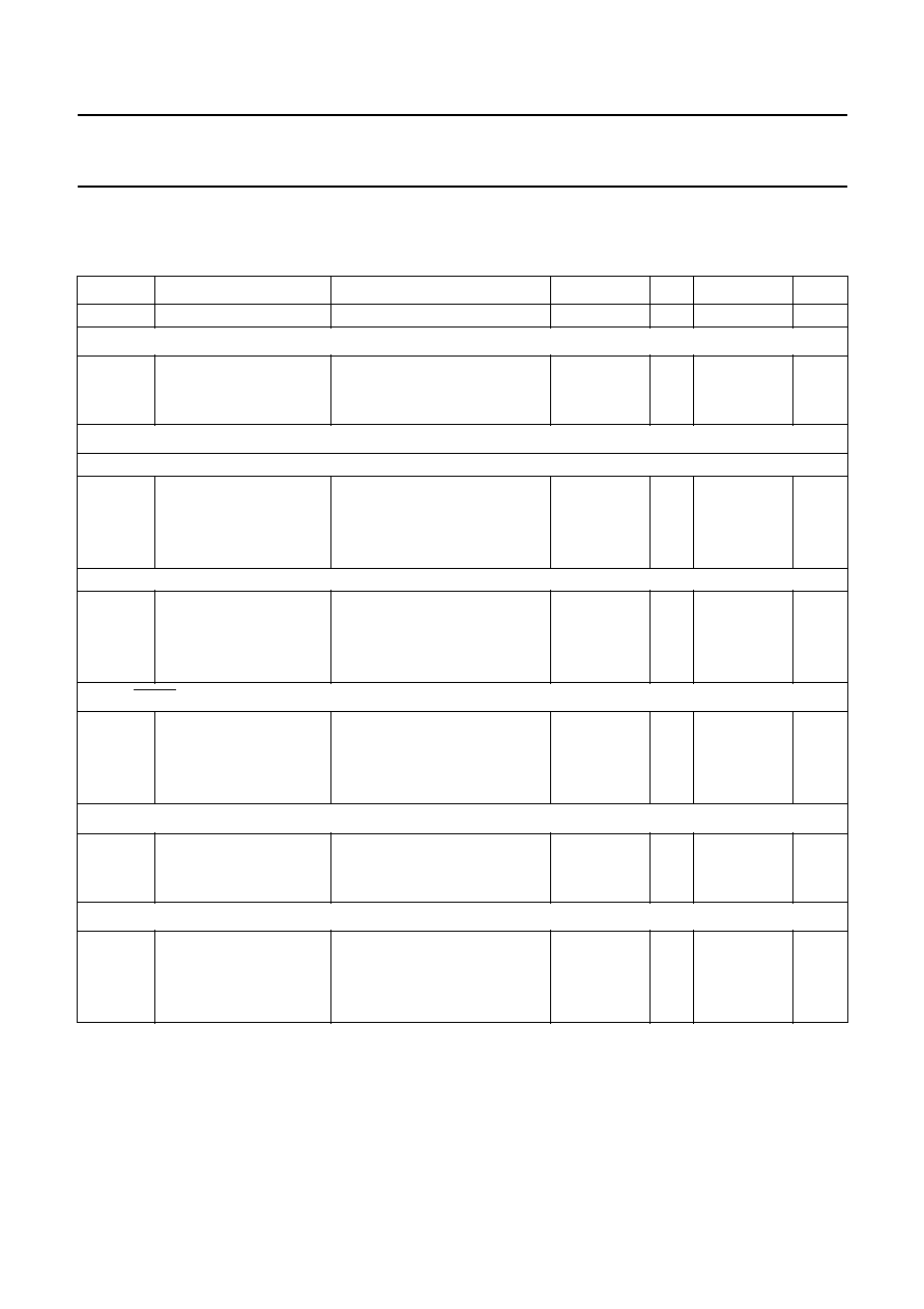
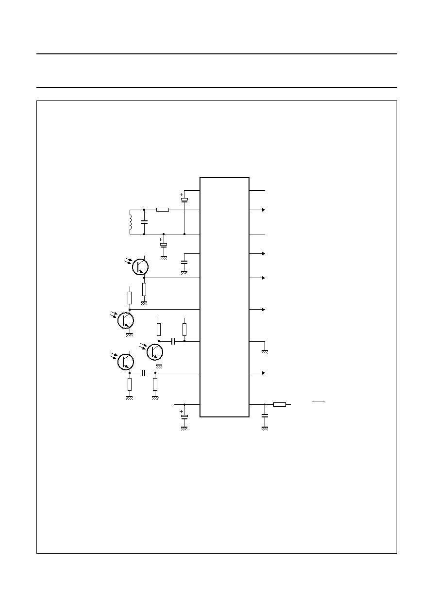
Fig.1 Block diagram.
handbook, full pagewidth
comparator 1
comparator 2
comparator 3
comparator 4
SAA1310
(SAA1310T)
Vref
POWER-ON AND
POWER-FAILURE
DETECTOR
AMPLIFIER
FILTER
DETECTOR
WRITE
AMPLIFIER
Vref
write
current
VP
GND
VP
comparator 1
non - inverting input
comparator 1
output
comparator 2
non - inverting input
comparator 2
output
comparator 3
inverting input
comparator 3
output
comparator 4
inverting input
comparator 4
output
power on/failure
output
power on/failure
capacitor
write/read
input
control head data
output
reference voltage
output
control head
input/output
control head
feedback
1
(1)
4
(4)
18
(20)
17
(19)
16
(18)
15
(17)
14
(15)
13
(14)
11
(12)
10
(11)
2
(2)
3
(3)
5
(6)
6
(7)
7
(8)
12 (13)
8
(9)
9 (10)
capstan reverse
input
MEA082 - 1
April 1995
4
Philips Semiconductors
Product specification
Control interface for VHS video recorders
SAA1310
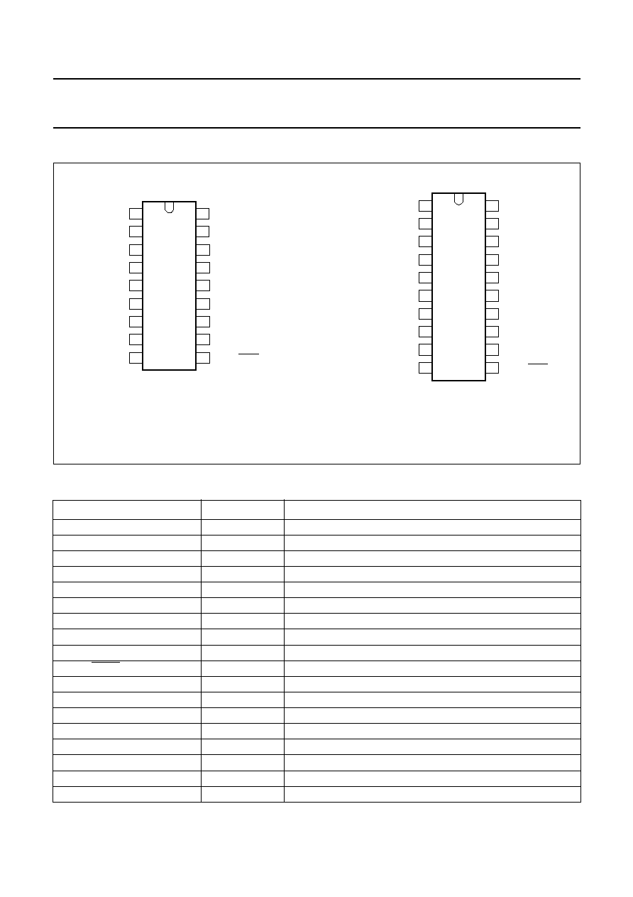
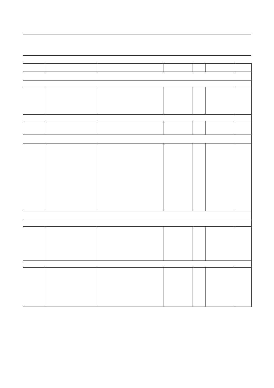
PIN CONFIGURATION
PINNING (pins in parenthesis refer to SAA1310T)
SYMBOL
PIN
DESCRIPTION
CTL FB
1
(1)
control head feedback
CTL I/O
2
(2)
control head input/output
V
ref
3
(3)
reference voltage output
CPO/FAIL
4
(4)
power on/failure capacitor
CIN1
5
(6)
comparator 1 input
CIN2
6
(7)
comparator 2 input
CIN3
7
(8)
comparator 3 input
CIN4
8
(9)
comparator 4 input
V
P
9
(10)
supply voltage
WRITE/READ
10
(11)
write/read input
COUT4
11
(12)
comparator 4 output
GND
12
(13)
ground
COUT3
13
(14)
comparator 3 output
COUT2
14
(15)
comparator 2 output
COUT1
15
(17)
comparator 1 input
CTL DATA
16
(18)
control head data output
PO/FAIL OUT
17
(19)
power on/failure output
CAPREV
18
(20)
capstan reverse input
dbook, halfpage
MEA083
1
2
3
4
5
6
7
8
9
18
17
16
15
14
13
12
11
10
CAPREV
PO/FAIL OUT
CTL DATA
COUT1
GND
COUT2
COUT3
COUT4
CTL FB
CTL I/O
Vref
CPO/FAIL
VP
CIN1
CIN2
CIN3
CIN4
SAA1310
WRITE/READ
handbook, halfpage
MEA084
1
2
3
4
5
6
7
8
9
10
20
19
18
17
16
15
14
13
12
11
CAPREV
PO/FAIL OUT
CTL DATA
COUT1
CTL FB
CTL I/O
Vref
CPO/FAIL
SAA1310T
VP
CIN1
CIN2
CIN3
CIN4
GND
COUT2
COUT3
COUT4
WRITE/READ
n.c.
n.c.
Fig.2 Pin configurations.
a. SAA1310.
b. SAA1310T.
April 1995
5
Philips Semiconductors
Product specification
Control interface for VHS video recorders
SAA1310
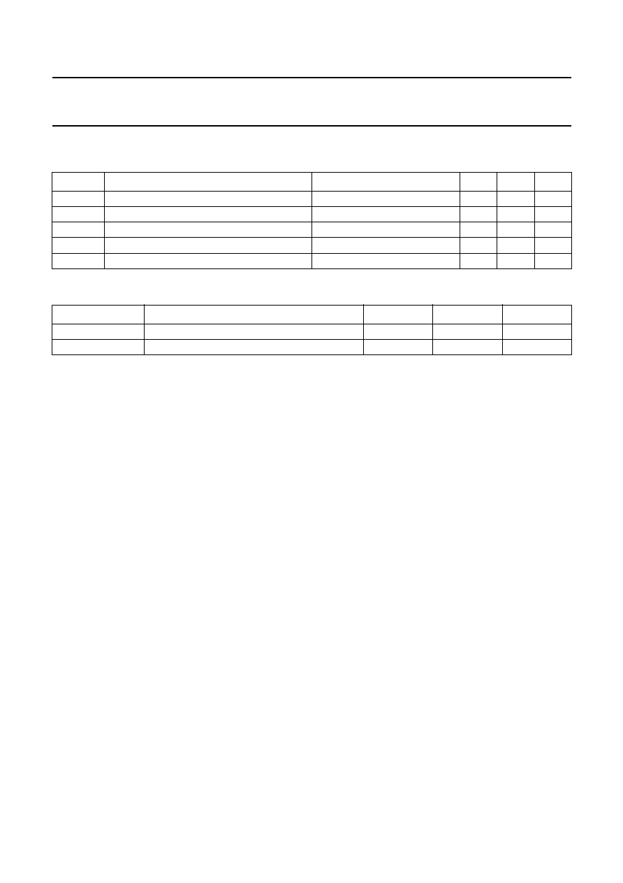
LIMITING VALUES (PIN NUMBERS IN PARENTHESIS REFER TO SAA1310T)
In accordance with the Absolute Maximum System (IEC 134)
THERMAL RESISTANCE
SYMBOL
PARAMETER
CONDITIONS
MIN.
MAX.
UNIT
V
P
supply voltage range
0
6.0
V
V
I
/V
O
voltage on all pins
except pins 11 (12) and 13 (14)
0
V
P
V
V
O
output voltage on pins 11 (12) and 13 (14)
0
18
V
T
stg
storage temperature range
-
65
+
150
∞
C
T
amb
ambient temperature range
0
+
70
∞
C
SYMBOL
PARAMETER
TYP.
MAX.
UNIT
R
th
thermal resistance (SAA1310)
75
-
K/W
R
th
thermal resistance (SAA1310T)
90
-
K/W
April 1995
6
Philips Semiconductors
Product specification
Control interface for VHS video recorders
SAA1310
CHARACTERISTICS (PIN NUMBERS IN PARENTHESIS REFER TO SAA1310T)
V
P
= 5 V; T
amb
= 25
∞
C; all voltage referenced to pin 12 (13); according to the test set-up (see Fig.4); unless otherwise
specified
SYMBOL
PARAMETER
CONDITION
MIN.
TYP.
MAX.
UNIT
P
d
power dissipation
note 1
-
85
-
mW
Supply pin 9 (10)
V
P
supply voltage
4.5
5.0
5.5
V
I
P
supply current
read mode
10
15
20
mA
write mode; duty factor = 50%
13
18
24
mA
CTL I/O pin 2 (2)
READ MODE PIN 10 (11)
<
0.5 V
V
I
input voltage (peak-to-
f = 500 Hz
0.35
-
-
mV
peak value)
f = 30 kHz; non-linear operation
-
-
200
mV
B
bandwidth low-pass filter
-
3
-
kHz
I
b
input bias current
read mode
-
0.1
-
µ
A
WRITE MODE PIN 10 (11)
>
3.5 V
V
O
output voltage LOW
I
CTL I/O
= 3 mA;
-
-
0.4
V
pin CTL DATA = HIGH
V
O
output voltage HIGH
I
CTL I/O
=
-
3 mA;
4.6
-
-
V
pin CTL DATA = LOW
WRITE/READ pin 10 (11)
V
I
input voltage
read mode
-
-
0.5
V
write mode; analog
1.6
-
3.3
V
I
I
input current
read mode
-
-
1.5
-
µ
A
write mode
-
0.1
-
µ
A
V
ref
pin 3 (3); note 2
V
O
output voltage
2.4
2.5
2.6
V
I
tot
total current
including write current
-
4
-
+
4
mA
R
O
output resistance
-
0.4
0.6
CAPREV pin 18 (20)
V
IH
input voltage HIGH
2.0
-
-
V
V
IL
input voltage LOW
-
-
0.8
V
I
IH
input current HIGH
V
CAPREV
= 5 V
-
-
10
µ
A
I
IH
input current LOW
V
CAPREV
= 0 V
-
10
-
-
µ
A
April 1995
7
Philips Semiconductors
Product specification
Control interface for VHS video recorders
SAA1310
CTL DATA pin 16 (18)
WRITE MODE
V
IH
input voltage HIGH
2.0
-
-
V
V
IL
input voltage LOW
-
-
0.8
V
I
IH
input current HIGH
V
CTL DATA
= 5 V
-
-
10
µ
A
I
IL
input current LOW
V
CTL DATA
= 0 V
-
10
-
-
µ
A
READ MODE
V
OL
output voltage LOW
I
OL
= 0.5 mA
-
-
0.4
V
V
OH
output voltage HIGH
I
OH
=
-
50
µ
A
2.4
-
-
V
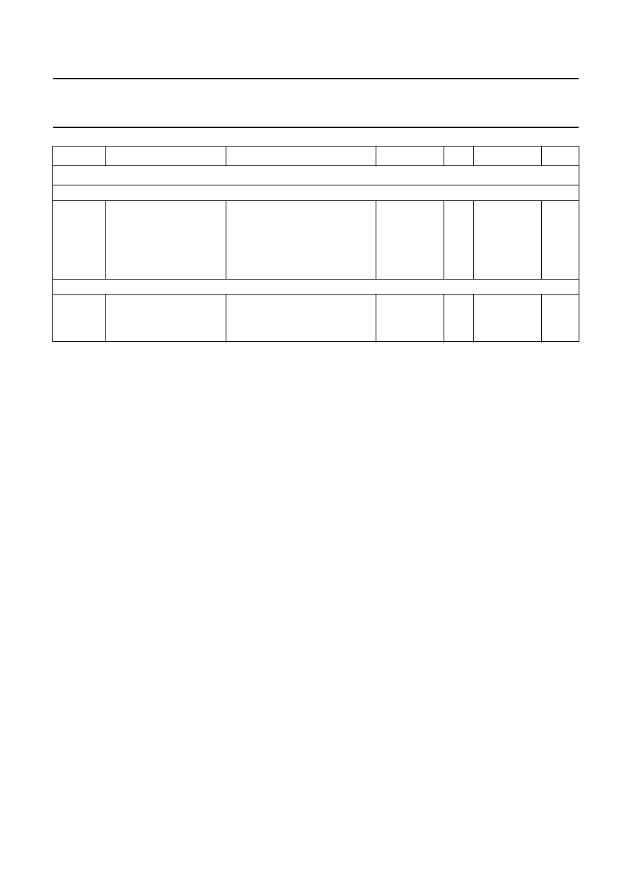
CPO/FAIL and PO/FAIL OUT pin 4 (4) and 17 (19); see Fig.3
V
O
operating voltage range
at decreasing V
P
1.5
-
5.5
V
V
OL
output voltage LOW
I
OL
= 1 mA
-
-
0.4
V
V
OH
output voltage HIGH
I
OH
= 1 mA
V
P
-
0.9
-
-
V
t
d
delay time
C
CAPREV
= 68 nF
-
50
-
ms
V
TL1
threshold level 1
4.5
-
4.8
V
V
TL2
threshold level 2
-
3.5
-
V
I
O
source current pin 4
-
-
3
-
µ
A
I
O
sink current pin 4
-
300
-
µ
A
V
O(min.)
minimum output voltage
-
20
-
mV
V
O(max.)
maximum output voltage
-
2.1
-
V
High output current type comparators
CIN3 and CIN4 pins 7 (8) and 8 (9)
V
hys
input hysteresis
-
10
-
mV
V
IL
input voltage LOW
-
-
V
ref
-
10 mV
V
V
IH
input voltage HIGH
V
ref
+
10 mV
-
-
V
I
IL
input current LOW
CIN3 = CIN4 = 0 V
-
1
-
-
µ
A
I
IH
input current HIGH
CIN3 = CIN4 = V
P
-
-
+
1
µ
A
COUT3 and COUT4 pins 13 (14) and 11 (12)
V
OL
output voltage LOW
I
OL
= 100 mA
-
-
1.0
V
I
OL
= 2 mA
-
-
0.4
V
±
I
OL
leakage current
output voltage HIGH;
COUT3 = COUT4 = 17 V
-
-
1
µ
A
t
tr
transient time
note 3
-
0.5
-
µ
s
T
j
thermal protection
-
130
-
∞
C
SYMBOL
PARAMETER
CONDITION
MIN.
TYP.
MAX.
UNIT
April 1995
8
Philips Semiconductors
Product specification
Control interface for VHS video recorders
SAA1310
Notes to the characteristics
1. Without the sink current of the comparators; in write mode.
2. Minimum value of capacitor connected to this pin is 4.7
µ
F.
3. V
i
= 100 mV p-p. Inputs connected to V
ref
via a 10 k
resistor; outputs connected to V
P
via a 250
resistor.
4. V
i
= 100 mV p-p. Inputs connected to V
ref
via a 10 k
resistor; outputs connected to V
P
via a 2.5 k
resistor.
Low output current type comparators
CIN1 AND CIN2 pins 5 (6) and 6 (7)
V
hys
input hysteresis
-
10
-
mV
V
IL
input voltage LOW
-
-
V
ref
-
10 mV
V
V
IH
input voltage HIGH
V
ref
+
10 mV
-
-
V
I
I
input current
CIN1 = CIN2 = 0 V
-
1
-
-
µ
A
CIN1 = CIN2 = V
P
-
-
+1
µ
A
COUT1 AND COUT2 pins 15 (17) and 14 (15)
V
OL
output voltage HIGH
I
OH
=
-
100
µ
A
4.5
-
-
V
V
OH
output voltage LOW
I
OL
= 2 mA
-
-
1
V
t
tr
transient time
note 4
-
0.5
-
µ
s
SYMBOL
PARAMETER
CONDITION
MIN.
TYP.
MAX.
UNIT

April 1995
9
Philips Semiconductors
Product specification
Control interface for VHS video recorders
SAA1310
MEA085
100
100
td
td
td
td
td
t
VP
V17 (19)
t
VTL1
VTL2
1.5 V
Fig.3 Power-ON and power-failure detector.
April 1995
10
Philips Semiconductors
Product specification
Control interface for VHS video recorders
SAA1310
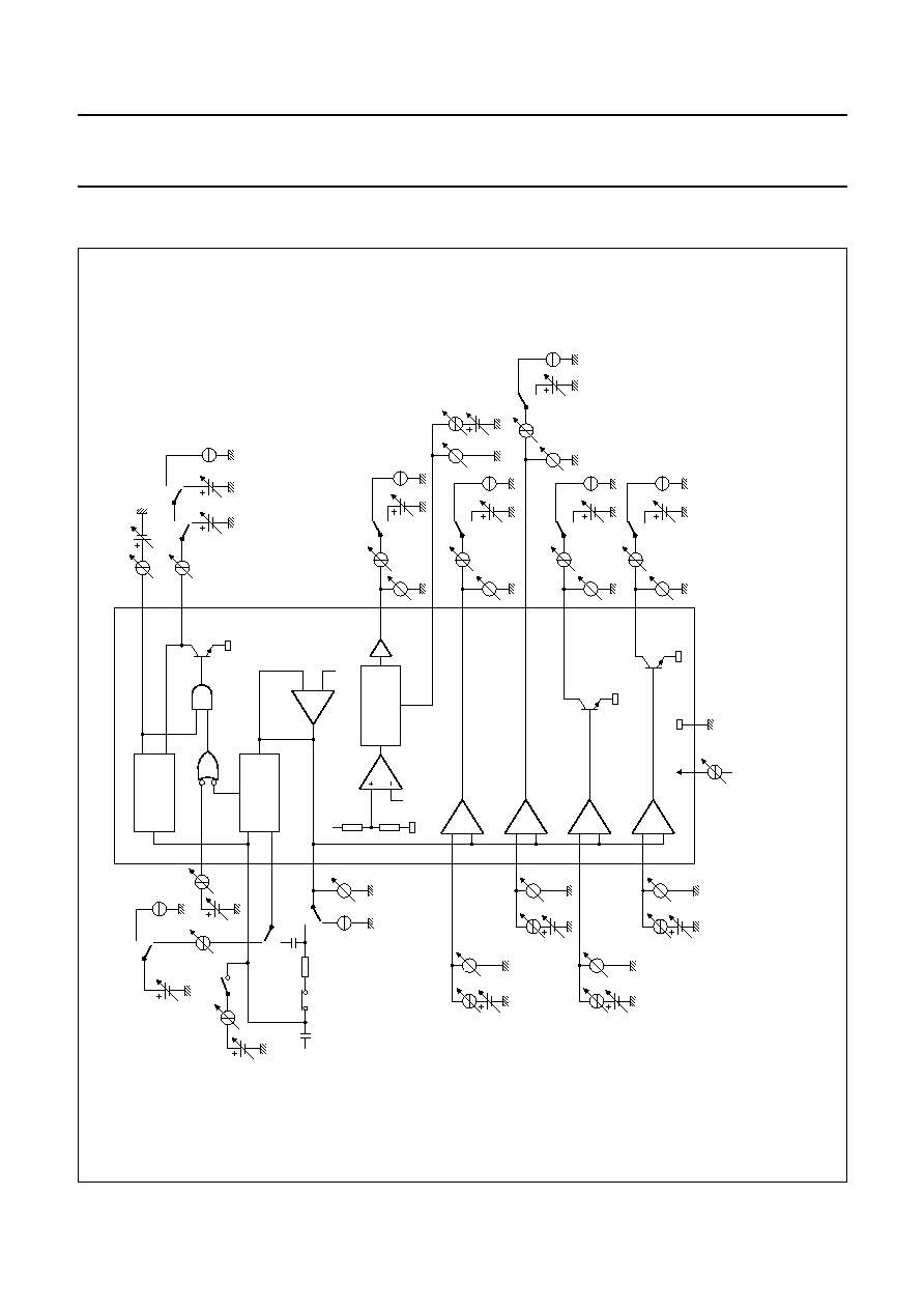
APPLICATION INFORAMTION
Fig.4 Test circuit diagram.
Pin numbers in parenthesis refer to the SAA1310T.
handbook, full pagewidth
MEA086 - 1
13
(14)
AMPLIFIER
FIL
TER
DETECT
OR
1
(1)
2
(2)
V
P
compar
ator 1
compar
ator 2
compar
ator 3
compar
ator 4
SAA1310
(SAA1310T)
WRITE
AMPLIFIER
wr
ite
current
GND
4
(4)
18
(20)
16
(18)
15
(17)
14
(15)
11
(12)
10
(11)
3
(3)
5
(6)
6
(7)
7
(8)
12(13)
8
(9)
9(10)
V
ref
PO
WER-ON AND
PO
WER-F
AILURE
DETECT
OR
V
P
17
(19)
-
-
+
+
-
+
-
+
-
+
IV
IV
IV
IV
V
I
V
I
I
82 nF
10
µ
F
650
V
i
I
R
W
I
V
I
V
I
V
I
V
I
I
V
ref
April 1995
11
Philips Semiconductors
Product specification
Control interface for VHS video recorders
SAA1310
handbook, full pagewidth
47
µ
F
4.7 nF
68
nF
47
µ
F
100
nF
47 k
+5 V
SAA1310
(SAA1310T)
1
(1)
2
(2)
3
(3)
4
(4)
5
(6)
6
(7)
7
(8)
18
(20)
17
(19)
16
(18)
15
(17)
14
(15)
13
(14)
12
(13)
VI
CTL head
47
µ
F
8
(9)
11
(12)
10
(11)
9
(10)
VI
VI
VI
VI
COUT4
COUT1
COUT2
COUT3
CAPREV
PO/FAIL OUT
CTL DATA
WRITE/READ
MEA087
Pin numbers in parenthesis refer to the SAA1310T.
Fig.5 Application diagram.
April 1995
12
Philips Semiconductors
Product specification
Control interface for VHS video recorders
SAA1310
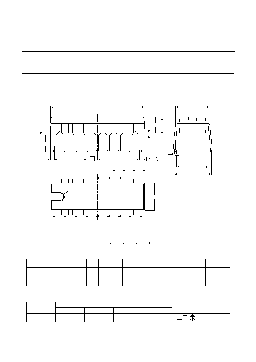
PACKAGE OUTLINES
REFERENCES
OUTLINE
VERSION
EUROPEAN
PROJECTION
ISSUE DATE
IEC
JEDEC
EIAJ
SOT102-1
93-10-14
95-01-23
UNIT
A
max.
1
2
b
1
(1)
(1)
(1)
b
2
c
D
E
e
M
Z
H
L
mm
DIMENSIONS (inch dimensions are derived from the original mm dimensions)
A
min.
A
max.
b
max.
w
M
E
e
1
1.40
1.14
0.53
0.38
0.32
0.23
21.8
21.4
6.48
6.20
3.9
3.4
0.254
2.54
7.62
8.25
7.80
9.5
8.3
0.85
4.7
0.51
3.7
inches
0.055
0.044
0.021
0.015
0.013
0.009
1.40
1.14
0.055
0.044
0.86
0.84
0.26
0.24
0.15
0.13
0.01
0.10
0.30
0.32
0.31
0.37
0.33
0.033
0.19
0.020
0.15
M
H
c
(e )
1
M
E
A
L
seating plane
A
1
w
M
b
1
b
2
e
D
A
2
Z
18
1
10
9
b
E
pin 1 index
0
5
10 mm
scale
Note
1. Plastic or metal protrusions of 0.25 mm maximum per side are not included.
DIP18: plastic dual in-line package; 18 leads (300 mil)
SOT102-1

April 1995
13
Philips Semiconductors
Product specification
Control interface for VHS video recorders
SAA1310
UNIT
A
max.
A
1
A
2
A
3
b
p
c
D
(1)
E
(1)
(1)
e
H
E
L
L
p
Q
Z
y
w
v
REFERENCES
OUTLINE
VERSION
EUROPEAN
PROJECTION
ISSUE DATE
IEC
JEDEC
EIAJ
mm
inches
2.65
0.30
0.10
2.45
2.25
0.49
0.36
0.32
0.23
13.0
12.6
7.6
7.4
1.27
10.65
10.00
1.1
1.0
0.9
0.4
8
0
o
o
0.25
0.1
DIMENSIONS (inch dimensions are derived from the original mm dimensions)
Note
1. Plastic or metal protrusions of 0.15 mm maximum per side are not included.
1.1
0.4
SOT163-1
10
20
w
M
b
p
detail X
Z
e
11
1
D
y
0.25
075E04
MS-013AC
pin 1 index
0.10
0.012
0.004
0.096
0.089
0.019
0.014
0.013
0.009
0.51
0.49
0.30
0.29
0.050
1.4
0.055
0.419
0.394
0.043
0.039
0.035
0.016
0.01
0.25
0.01
0.004
0.043
0.016
0.01
0
5
10 mm
scale
X
A
A
1
A
2
H
E
L
p
Q
E
c
L
v
M
A
(A )
3
A
SO20: plastic small outline package; 20 leads; body width 7.5 mm
SOT163-1
95-01-24
97-05-22

April 1995
14
Philips Semiconductors
Product specification
Control interface for VHS video recorders
SAA1310
SOLDERING
Introduction
There is no soldering method that is ideal for all IC
packages. Wave soldering is often preferred when
through-hole and surface mounted components are mixed
on one printed-circuit board. However, wave soldering is
not always suitable for surface mounted ICs, or for
printed-circuits with high population densities. In these
situations reflow soldering is often used.
This text gives a very brief insight to a complex technology.
A more in-depth account of soldering ICs can be found in
our
"IC Package Databook" (order code 9398 652 90011).
DIP
S
OLDERING BY DIPPING OR BY WAVE
The maximum permissible temperature of the solder is
260
∞
C; solder at this temperature must not be in contact
with the joint for more than 5 seconds. The total contact
time of successive solder waves must not exceed
5 seconds.
The device may be mounted up to the seating plane, but
the temperature of the plastic body must not exceed the
specified maximum storage temperature (T
stg max
). If the
printed-circuit board has been pre-heated, forced cooling
may be necessary immediately after soldering to keep the
temperature within the permissible limit.
R
EPAIRING SOLDERED JOINTS
Apply a low voltage soldering iron (less than 24 V) to the
lead(s) of the package, below the seating plane or not
more than 2 mm above it. If the temperature of the
soldering iron bit is less than 300
∞
C it may remain in
contact for up to 10 seconds. If the bit temperature is
between 300 and 400
∞
C, contact may be up to 5 seconds.
SO
R
EFLOW SOLDERING
Reflow soldering techniques are suitable for all SO
packages.
Reflow soldering requires solder paste (a suspension of
fine solder particles, flux and binding agent) to be applied
to the printed-circuit board by screen printing, stencilling or
pressure-syringe dispensing before package placement.
Several techniques exist for reflowing; for example,
thermal conduction by heated belt. Dwell times vary
between 50 and 300 seconds depending on heating
method. Typical reflow temperatures range from
215 to 250
∞
C.
Preheating is necessary to dry the paste and evaporate
the binding agent. Preheating duration: 45 minutes at
45
∞
C.
W
AVE SOLDERING
Wave soldering techniques can be used for all SO
packages if the following conditions are observed:
∑
A double-wave (a turbulent wave with high upward
pressure followed by a smooth laminar wave) soldering
technique should be used.
∑
The longitudinal axis of the package footprint must be
parallel to the solder flow.
∑
The package footprint must incorporate solder thieves at
the downstream end.
During placement and before soldering, the package must
be fixed with a droplet of adhesive. The adhesive can be
applied by screen printing, pin transfer or syringe
dispensing. The package can be soldered after the
adhesive is cured.
Maximum permissible solder temperature is 260
∞
C, and
maximum duration of package immersion in solder is
10 seconds, if cooled to less than 150
∞
C within
6 seconds. Typical dwell time is 4 seconds at 250
∞
C.
A mildly-activated flux will eliminate the need for removal
of corrosive residues in most applications.
R
EPAIRING SOLDERED JOINTS
Fix the component by first soldering two diagonally-
opposite end leads. Use only a low voltage soldering iron
(less than 24 V) applied to the flat part of the lead. Contact
time must be limited to 10 seconds at up to 300
∞
C. When
using a dedicated tool, all other leads can be soldered in
one operation within 2 to 5 seconds between
270 and 320
∞
C.

April 1995
15
Philips Semiconductors
Product specification
Control interface for VHS video recorders
SAA1310
DEFINITIONS
LIFE SUPPORT APPLICATIONS
These products are not designed for use in life support appliances, devices, or systems where malfunction of these
products can reasonably be expected to result in personal injury. Philips customers using or selling these products for
use in such applications do so at their own risk and agree to fully indemnify Philips for any damages resulting from such
improper use or sale.
Data sheet status
Objective specification
This data sheet contains target or goal specifications for product development.
Preliminary specification
This data sheet contains preliminary data; supplementary data may be published later.
Product specification
This data sheet contains final product specifications.
Limiting values
Limiting values given are in accordance with the Absolute Maximum Rating System (IEC 134). Stress above one or
more of the limiting values may cause permanent damage to the device. These are stress ratings only and operation
of the device at these or at any other conditions above those given in the Characteristics sections of the specification
is not implied. Exposure to limiting values for extended periods may affect device reliability.
Application information
Where application information is given, it is advisory and does not form part of the specification.