 | –≠–ª–µ–∫—Ç—Ä–æ–Ω–Ω—ã–π –∫–æ–º–ø–æ–Ω–µ–Ω—Ç: SAA1501T | –°–∫–∞—á–∞—Ç—å:  PDF PDF  ZIP ZIP |

DATA SHEET
Objective specification
File under Integrated Circuits, IC11
December 1994
INTEGRATED CIRCUITS
Philips Semiconductors
SAA1501T
Battery charge level indicator

December 1994
2
Philips Semiconductors
Objective specification
Battery charge level indicator
SAA1501T
FEATURES
∑
High level of integration to allow assembly in intelligent
battery packs
∑
Accurate charge and discharge account
∑
Large dynamic range of charge and discharge currents
∑
Independent settings of charge and discharge efficiency
∑
2 V minimum supply voltage (2 cell operation)
∑
Temperature protection of batteries during charging
∑
Temperature controlled self-discharge
∑
Accurate charge current regulation
∑
Two charge amount display modes, LCD and LED.
GENERAL DESCRIPTION
The SAA1501T is intended to be used as a battery monitor
and charge current control circuit in rechargeable battery
systems.
The SAA1501T is processed in BiCMOS technology
where the benefits of mixed bipolar and CMOS technology
is fully utilized to achieve high accuracy measurements
and digital signal processing in the same device. The
general function of the integrated circuit is a Coulomb
counter. During battery charging, the charge current and
charge time are registered in a Coulomb counter. During
discharge, the discharge current and time are recorded.
The momentary charge amount of the batteries can be
displayed either on an LCD screen or on an LED bargraph.
Using the SAA1501T, intelligent batteries or intelligent
battery powered systems can be easily designed with only
a few external components.
QUICK REFERENCE DATA
ORDERING INFORMATION
SYMBOL
PARAMETER
CONDITIONS
MIN.
TYP.
MAX.
UNIT
V
CC
supply voltage
2.0
3.0
4.3
V
I
CC
supply current
V
CC
= 3 V;
I
c
= I
d
= 60
µ
A
-
1.2
1.7
mA
I
CCstb
supply current in standby mode
V
CC
= 3 V;
V
CSI
= V
DSI
= 0 V
-
-
100
µ
A
f
osc
fixed oscillator frequency
C
osc
= 820 pF;
R
ref
= 51.5 k
-
4.2
-
kHz
V
i(s)
input sense voltage (pins 9 and 10)
0
-
V
CC
-
1.6 V
T
amb
operating ambient temperature
0
-
+70
∞
C
TYPE NUMBER
PACKAGE
NAME
DESCRIPTION
VERSION
SAA1501T
SO24
plastic small outline package; 24 leads; body width 7.5 mm
SOT137-1

December 1994
3
Philips Semiconductors
Objective specification
Battery charge level indicator
SAA1501T
BBBB
BBBB
BBBB
BBB
BBB
BBB
BBBB
BBBB
BBBB
BBBB
BBBB
BBB
BBB
BBB
BBB
BBB
BBB
BBB
BBB
BBB
BBB
BBB
BBB
BBB
B
B
B
B
B
BBBBBBB
BBBBBBB
B
B
B
B
B
BBB
BBB
BBB
BBB
BBB
BBB
BBB
BBB
BBB
BBB
B
B
B
B
BBB
BBB
BBBB
BBBB
BBBB
BB
BB
BB
BBB
BBB
BBB
BBB
BBB
BBB
BBB
BBB
BBB
BBB
BBB
BBB
BBB
BBB
BBB
BBB
BLOCK DIAGRAM
Fig.1 Block diagram.
December 1994
4
Philips Semiconductors
Objective specification
Battery charge level indicator
SAA1501T
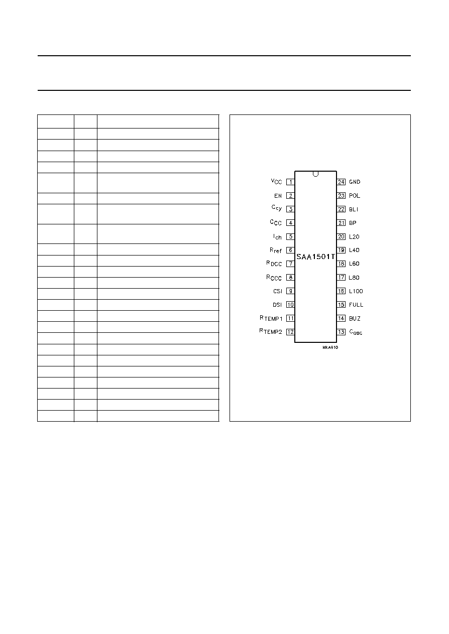
PINNING
SYMBOL
PIN
DESCRIPTION
V
CC
1
supply voltage
EN
2
enable output
C
cy
3
duty cycle capacitor output
C
CC
4
charge counter capacitor output
I
ch
5
maximum average charge current
setting input
R
ref
6
current reference resistor input
R
DCC
7
discharge current conversion resistor
input
R
CCC
8
charge current conversion resistor
input
CSI
9
charge sense input
DSI
10
discharge sense input
R
TEMP1
11
temperature sensing resistor 1 input
R
TEMP2
12
temperature sensing resistor 2 input
C
osc
13
oscillator capacitor input
BUZ
14
buzzer output
FULL
15
battery full indication output
L100
16
100% segment indication output
L80
17
80% segment indication output
L60
18
60% segment indication output
L40
19
40% segment indication output
L20
20
20% segment indication output
BP
21
LCD back plane drive
BLI
22
battery low indicator LED output
POL
23
power-on LED output
GND
24
power ground
Fig.2 Pin configuration.

December 1994
5
Philips Semiconductors
Objective specification
Battery charge level indicator
SAA1501T
FUNCTIONAL DESCRIPTION
The most important function of the SAA1501T is the
charge account in rechargeable battery systems. Both
NiCd and NiMH batteries in all sizes can be used. The
system can operate alone as a charge monitor with a
charge amount display function or, can operate in
conjunction with a charger. If the SAA1501T operates
together with a charger, it delivers a control signal at output
EN, for charge current regulation or for battery voltage
regulation.
Fast charging systems and charge current regulation
The SAA1501T is especially designed to be used in fast
charging systems. In fast charging systems, the charge
time is lowered by raising the charge current. Signal EN
controls the charger current. The counters register the
state of charge of the batteries and at the 80% level the
charge current is reduced via a smaller duty cycle
regulation of signal EN. The second (slow) level fully
charges the batteries which is not possible with the first
(fast) level. After the slow charge mode the counter
switches over to an even smaller duty cycle of EN and thus
enters the third (trickle) charge mode, to overcome the
self-discharge of the batteries.
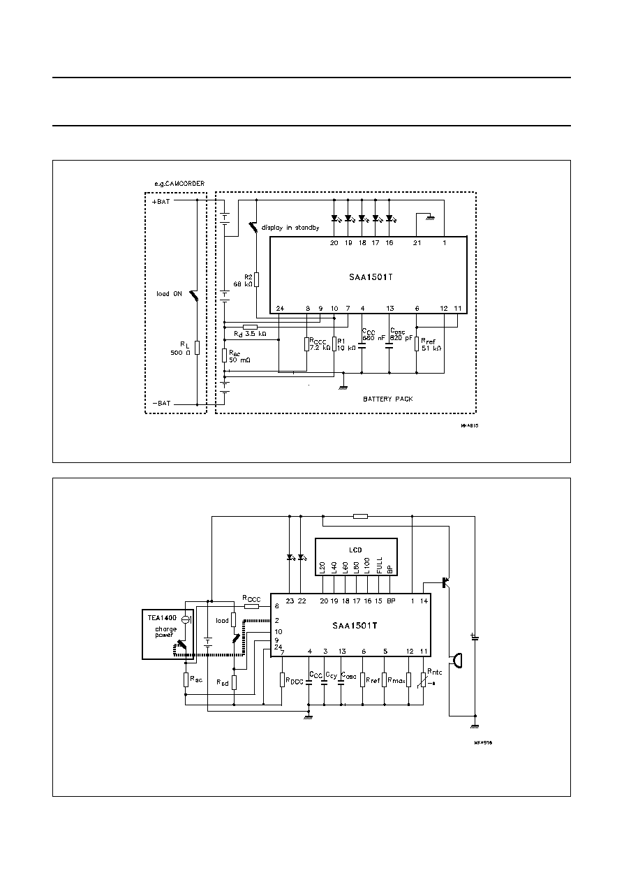
Current sensing and charge account
The charge current is sensed by means of a very low
resistance (e.g. 70 m
) sense resistor R
sc
(see Fig.8) to
save power at high charge rates. Via the V/I charge
converter and external resistor R
CCC
(see Fig.8), the
sensed voltage is converted into a charge current I
c
(the
same is applicable for the discharge current). In the I/F
converter the charge current is converted into a frequency
for up-counting the counter. For the discharge current (I
d
)
the converted frequency is used for down-counting. The
up and down counting is registered in counters CNT1 and
CNT2, depending on the actual charge and discharge
current levels of the batteries. This is called dynamic
charge account.
Charge display
The charge amount represented by the Coulomb counter
can be displayed via an LCD screen or via an LED
bargraph. If the charge amount is reduced to 0%, the
battery low indicator (BLI) LED is turned on at the end of a
battery discharge session. A flashing BLI, in combination
with a repeating buzzer alarm, informs the user about the
low charge state. A new charge session should then be
started.
Protections
In the temperature control block, the absolute temperature
is used as a protection to end the fast charge cycle. Fast
charging at high temperature is not permitted because of
degradation of the battery cells. If the batteries are
disconnected, an open-battery condition is recognized and
the SAA1501T enters the standby mode.
Mode detection
The mode detector detects whether there are any charge
or discharge currents, whether the system is powered,
whether loads are connected or whether the system is in
the standby mode. If power is connected, the power-on
LED (POL) is on. In the standby mode, the Coulomb
counter will count down in accordance with the
self-discharge speed of the batteries, which is temperature
controlled. The following subsections describe the various
blocks of the block diagram in more detail.
Supply and reference
During the period when V
CC
rises from 0 V to the internal
reset level, all counters are reset. The internal reset is
released before V
CC
reaches 1.7 V. The operating supply
voltage ranges from 2 V to the open battery level of
4.3 V (min). The characteristics are guaranteed at
V
CC
= 3 V. In order to protect the SAA1501T against high
supply voltages during open battery in a flyback converter,
a voltage clamp circuit is made active at 6.35 V (typ). The
clamping current must not exceed 80 mA. A band gap
reference block is included to generate accurate voltages
i.e. for the oscillator. Moreover, together with R
ref
, accurate
currents are generated which are used in the I/F and V/I
converters and the oscillator block. In the standby mode
only the oscillator and the digital parts are active to limit the
discharge current of the batteries to a current level of less
than 100 mA. The circuits that are needed temporarily are
switched on and off during standby (see "Timing
characteristics" t
som
).
Voltage-to-current charge and discharge
In the V/I converter, the input charge current is translated
into acceptable levels for the circuit. The conversion
formula is:
; where R
CCC
> R
sc
(see Fig.7)
I
c
I
ch
e
arg
R
sc
◊
(
)
R
CCC
---------------------------------------
=

December 1994
6
Philips Semiconductors
Objective specification
Battery charge level indicator
SAA1501T
With R
CCC
, the charge efficiency can be manipulated
depending on the charge level. The restriction of the
SAA1501T is a maximum average charge current of 60
µ
A
and a minimum momentary charge current of 0.6
µ
A. The
same formula is applicable for the discharge current. The
discharge efficiency can now also be changed by R
DCC
depending on the discharge current levels, but
independent of the charge current. As both sense levels
are referenced to ground, the sensing elements could be
combined into one. The outputs are used combined as
1
/
6
◊
(I
c
-
I
d
) in the I/F converter and combined as (I
c
-
I
d
)
in the pulse width modulator block and made separately
available in the mode detector. The conversion is made
lower by a factor of 6 in the I/F converter block, thereby
enabling the use of poor leakage capacitors on pin 4. All
V/I converter pins are sensitive to capacitive loading
(C
out
◊
R
conv
< 1 ms), the conversion resistors should be
mounted as close as possible to the output pins.
I/F converter
This block produces up-counts while charging and
down-counts while discharging. The I/F converter
translates the charge/discharge currents into a frequency.
This frequency is determined by
During the time period `t', the charge current, expressed as
a `Charge Parcel', will be counted in the Coulomb counters
(CNT1 and CNT2). During discharge the `Charge Parcel' is
the product of the discharge current and the `t' from the I/F
converter generated frequency. The momentary contents
of the Coulomb counter is a multiple of the `Charge
Parcels'.
Coulomb counters CNT1 and CNT2
The SAA1501T has been designed for average maximum
charge and discharge current levels of 5 C and minimum
charge and discharge current levels of 0.05 C. This means
that counter CNT1 will be full, or empty, after a minimum
time period of 12 minutes at maximum charge and
discharge currents at the recommended oscillator
frequency. Higher charge and discharge rates than 5 C
are possible, but only by changing the oscillator frequency.
It should be noted that the self-discharge time and the
display functions are influenced by a higher oscillator
frequency. The SAA1501T enables top-up charging in
order to account for the decrease of charge efficiency at
high charge rates. The SAA1501T switches to the slow
charge mode at full recognition when CNT1 is at its
maximum. As soon as the batteries are completely full
(when CNT2 is at its maximum), the SAA1501T switches
f
I
(
c d
( )
R
sense
6
)
◊
◊
C
(
CC
V
osc
R
CCC RDCC
(
)
)
◊
◊
------------------------------------------------------------------------------------
=
to the trickle charge mode to overcome the self-discharge
of the batteries. The top-up charge volume of
CNT2 = 0.2
◊
CNT1 = 0.2 C (where Q is rated as Ampere
hours of the battery). The slow and trickle charge current
levels are dependent on the k-factor. Signal EN controls
the external charger e.g. TEA1400 (see Fig.8). When an
LED bargraph display is used, the LED currents are also
considered as a battery discharge current, and therefore
influence the duty cycle of the charge current regulation
signal EN. The SAA1501T also enables temperature
protection. In the event that the battery temperature
exceeds a certain maximum temperature level
(T
battery
> T
max
), which can be set by an external NTC
resistor, the SAA1501T switches to the slow charge mode.
In the standby mode (self-discharge mode), which is
recognized by the SAA1501T in the mode detector when
both the charge and discharge currents are zero
(I
c
= I
d
= 0), the self-discharge of the batteries is registered
by counting down in 200 days (based on f
osc
= 4 kHz) if
T
battery
< T
self
or in 100 days (based on f
osc
= 4 kHz) if
T
battery
> T
self
. T
self
is also set by means of an external NTC
resistor.
Band gap generation
From the band gap voltage block, two reference voltages
are derived V
ref
and V
max
. Voltage V
ref
at pin R
ref
sets the
reference currents, I
ref1
(I/F converter); I
ref2
(mode
detector) and I
ref3
(oscillator). Voltage V
max
sets the
current I
max
which is used in the pulse width modulation
block to accurately control the charge current.
Charge current regulation
While charging, the SAA1501T produces a charge current
regulation signal EN in the pulse width modulation block
which is used for controlling an external charger. This
digital signal EN is derived from the signal produced at pin
C
cy
. The duty cycle is determined by
in which the value of k depends on the state of the
counters CNT1 and CNT2:
CNT1 is not full; k = 1 (fast charging).
CNT1 is full; CNT2 is not full; k = 0.1 (slow charging).
CNT1 and CNT2 are full; k = 0.025 (trickle charging).
k
I
max
◊
I
c
I
d
≠
--------------------
=

December 1994
7
Philips Semiconductors
Objective specification
Battery charge level indicator
SAA1501T
Mode detector
This block differentiates between the available modes of
operation. The modes are given below:
Charge mode; power charge (POCH).
Discharge mode; battery load (BATLD).
Power load mode (POLD); the batteries are charged
while the load is also active.
Self discharge mode; (STANDBY).
To detect power in a regulated system (see Fig.8) the EN
signal is used for sensing. The POCH mode is recognized
when the converted charge current I
c
> I
ref2
(when in the
power mode, change of mode can only be recognised if
EN is HIGH). The BATLD mode is recognized when
I
d
> I
ref2
; the POLD mode is recognized when I
c
> I
ref2
and
I
d
> I
ref2
; the standby mode is recognized when I
c
< I
ref2
and I
d
< I
ref2
. In the standby mode, if the advised frequency
(4 kHz) is applied, it takes 0.5 s to determine another
mode (in all other modes, a change of mode is sensed
continuously). In all other modes an eventual change of
mode is done continuously. To save supply current during
standby, the V/I converters are switched off. With the
specific fixed intervals, the SAA1501T checks whether
power or load is connected again. This checking is
synchronized by the sensing signal of the V/I converters.
The SAA1501T can handle a DC charge current as well as
a discontinuous charge current (SMSP charger). The load
current can also be DC or interrupted, e.g. produced by a
motor. The digital filtering of both signals, to overcome
faulty mode detections, restricts the conditions in which
power and load are recognized. Because of the very
sensitive input detection level of the mode detector for a
charge current (power) in combination with the high
interference levels of motor driving, the detection level for
power (I
c
> I
ref2
) is raised by a factor of 25 when the
batteries are loaded.
Oscillator
As the oscillator has to operate in all modes, including the
standby mode, the current consumption of the oscillator
must be very low. The same applies for the band gap
generator block, because the band gap delivers accurate
reference voltages and currents to the oscillator block.
Apart from the low current consumption, the accuracy of
the period time is important. The period time of the
oscillator is:
t
osc
2
C
osc
◊
V
H
V
L
≠
(
)
I
ref3
---------------------------
5.6
C
osc
R
ref
◊
◊
=
◊
=
Prescaler/controller
In the prescaler, a new system clock is created (CLK)
which is used for all timing blocks. Many frequencies are
derived from the basic oscillator at the standard frequency
of 4 kHz (1/T
osc
), such as the self-discharge times and the
modulation frequency for the buzzer, the drive voltage
frequency for the LCD screen and the pulse trains for
temperature measurements and power/load sensing
measurements in the mode detector.
Temperature
In the temperature control block two temperature
measurements are performed. In order to switch off fast
charging when the battery temperature exceeds an
adjustable maximum temperature (T
max
), a maximum
temperature measurement is performed. A second
temperature measurement is performed in the standby
mode. This temperature measurement is input to the
temperature control block to switch over the self-discharge
rate from a count down of 200 days (based on f
osc
= 4 kHz)
if T
battery
< T
self
, to a count down rate of 100 days (based
on f
osc
= 4 kHz) if T
battery
> T
self
. In all modes the
temperature is measured periodical. The temperature
circuit which controls the above mentioned functions is a
bridge configuration synthesis, as illustrated in Fig.3.
Fig.3 Temperature circuit.

December 1994
8
Philips Semiconductors
Objective specification
Battery charge level indicator
SAA1501T
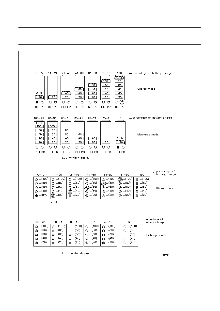
Display decoder driver
The counters are used to output the battery charge
amount via a decoder and driver stage to the display
outputs L100, L80, L60, L40 and L20 to drive an LCD
screen or an LED bargraph. A 64 Hz (based on
f
osc
= 4 kHz) block signal at output BP (back plane) must
be connected to the back plane of the LCD bar. If pin BP
is connected to ground, the display outputs L20 to L100
will produce signals for an LED bargraph. Output signal
POL (power-on LED) indicates when the batteries are in
the charge mode. When the counter is not at its maximum
state, POL is on and flickers at 2 Hz (based on
f
osc
= 4 kHz) when the counter is at its maximum. The
waveforms illustrated in Fig.4 depict operation of the
monitor display. The outputs BLI (battery low indication),
BUZ (buzzer) and FULL indicate the extreme status
(empty or full) of the counters and the batteries. The
waveforms of the signals BLI and BUZ if one switches over
from BATLD to standby when BLI is active, are given in
Fig.4.
The BLI sequence is as follows. If during discharge the
charge state falls below 0%, the red BLI LED is turned on.
Changing mode from discharge to standby means that the
BLI LED and the buzzer (BUZ) are activated as indicated
in Fig.4. If after a 0% passing recharge is activated, the red
BLI LED is turned on again for as long as the counter
remains below 10%. Switch-over in the 0 to 10% range to
standby will activate BLI and BUZ again.
The LEDs of the LED bargraph are activated as a result of
each operational mode change, starting with a step-up
pattern. Step-up means that LEDs are activated
successively one after the other, in accordance with the
charge status each
1
/
8
s (based on f
osc
= 4 kHz). After the
step-up, the LEDs will be on for 8 s (based on
f
osc
= 4 kHz), except for the POCH mode, where the LEDs
will be on continuously to inform the user about the charge
state of the batteries. The LCD display is, apart from the
LED mode, always visible.
Figure 5 shows the legend for Fig.6. Figure 6 shows the
operation of the monitor display.
BUZ
Fig.4 BLI and buzzer timing.

December 1994
9
Philips Semiconductors
Objective specification
Battery charge level indicator
SAA1501T
Open battery protection
Open battery protection is active when V
CC
= 4.5 V (typ.).
The SAA1501T will then react as if the system is in the
standby mode. This means that the LEDs are turned off in
the LED mode, in the LCD mode the flickering is stopped
and the enable pin (EN) is switched to floating.
Testing
A user test facility is built-in for checking if the LCD and/or
LED displays are mounted correctly. Pin R
CCC
is used as
a test pin. Raising the voltage above 1 V during the set-up
time will activate the test. The test mode can only be
started in the standby mode. In the test mode all counters
are reset and will be active successively in the sequence
BLI, L20, L40, L60, L80, L100 and FULL with an interval
period determined by T
osc
. The test mode can be exited via
the following methods:
Power-on; the Coulomb counter retains the latest data
displayed.
Automatically after the test cycle time; the Coulomb
counter is reset.
Fig.5 Legend for Fig.6.
December 1994
10
Philips Semiconductors
Objective specification
Battery charge level indicator
SAA1501T
Fig.6 Charge state of counter shown by LCD or LED display.

December 1994
11
Philips Semiconductors
Objective specification
Battery charge level indicator
SAA1501T
LIMITING VALUES
In accordance with the Absolute Maximum Rating System (IEC 134). All voltages with respect to GND (pin 24); input
currents are positive; pins 5, 6 and 21 are not allowed to be voltage driven; the voltage ratings are valid provided other
ratings are not being violated.
QUALITY SPECIFICATION
In accordance with SNW-FQ-611 part E. The numbers of the quality specification can be found in the "
Quality Reference
Handbook". The Handbook can be ordered using the code 9398 510 63011.
THERMAL CHARACTERISTICS
SYMBOL
PARAMETER
CONDITIONS
MIN.
MAX.
UNIT
V
CC
supply voltage
-
0.5
+5.5
V
V
n1
input voltage at pins 9 to 12
-
0.5
+1.0
V
V
n2
input voltage at pins 2 to 4, 13 to 20, 22
and 23
-
0.5
V
CC
V
V
voltage difference between pins 10 and
7 and between pins 9 and 8
-
2.0
+2.0
V
I
CC
supply current
-
80
mA
I
GND
power ground supply current
-
-
80
mA
I
n
supply current at pins 5 to 8
-
-
1
mA
P
tot
total power dissipation
T
amb
= 70
∞
C
-
0.75
W
T
stg
storage temperature
-
55
+150
∞
C
T
j
junction temperature
-
+150
∞
C
T
amb
operating ambient temperature
-
10
+75
∞
C
SYMBOL
PARAMETER
VALUE
UNIT
R
th j-a
thermal resistance from junction to ambient in free air
75
K/W

December 1994
12
Philips Semiconductors
Objective specification
Battery charge level indicator
SAA1501T
CHARACTERISTICS
V
CC
= 3 V; T
amb
= 25
∞
C; R
ref
= 51.5 k
(0.1%); C
osc
= 820 pF (0.1%); R
CCC
= R
DCC
= 3.65 k
(0.1%); R
max
= 3.48 k
(0.1%); I
ref
= V
ref
/R
ref
; I
max
= V
max
/R
max
; the minimum and maximum values are 4 sigma limits; unless otherwise
specified.
SYMBOL
PARAMETER
CONDITIONS
MIN.
TYP.
MAX.
UNIT
Supply
V
CC
supply voltage
note 1
2.0
3.0
4.3
V
V
CC(ir)
supply voltage internal
reset
-
1.2
1.7
V
I
CC
supply current
I
c
= I
d
= 60
µ
A
0.6
-
1.7
mA
I
CCstb
supply current in standby
mode
V
CSI
= V
DSI
= 0 V
-
-
100
mA
V
ref
reference voltage
note 2
204
211
217
mV
I
ref
reference current
notes 1 and 2
3.5
-
8
µ
A
V
max
maximum voltage
note 2
204
211
217
mV
TC
temperature coefficient of
reference voltage
T = 0 to 100
∞
C
0
25
◊
10
-
6
100
◊
10
-
6
∞
C
V
clamp
clamping level voltage
I
CC
= 50 mA
5.8
6.3
6.8
V
Voltage-to-current charge/discharge
I
4
voltage-to-current
charge/discharge current
accuracy
V
9
= 7 mV; V
4
= 1.5 V
-
259
-
324
-
389
nA
V
10
= 7 mV; V
4
= 1.5 V
262
328
394
nA
V
9
= 200 mV; V
4
= 1.5 V
-
8.93
-
9.13
-
9.32
µ
A
V
10
= 200 mV; V
4
= 1.5 V
8.93
9.13
9.32
µ
A
I
3
voltage-to-current
charge/discharge current
accuracy
V
9
= 7 mV; R
max
= 400 k
;
k = 0.025
-
1.55
-
1.94
-
2.32
µ
A
V
10
= 7 mV; R
max
= 400 k
;
k = 0.025
1.57
1.97
2.36
µ
A
V
9
= 200 mV;
R
max
= 400 k
; k = 0.025
-
53.5
-
54.7
-
56
µ
A
V
10
= 200 mV;
R
max
= 400 k
; k = 0.025
53.5
54.7
56
µ
A
I
4
/I
3
relative current accuracy
of voltage-to-current in
charge counter capacitor
V
9
= V
10
= 200 mV
-
1.0
2.5
%
V
i(s)
input sense voltage at
pins 9 and 10
V
CC(max)
= 3.7 V; note 1
0
-
V
CC
-
1.6
V
3.7 < V
CC
< 4.4 V; note 1
-
-
2.1
V
I
o(s)
DC output sense current
(pins 8 and 7)
0.6
-
60
µ
A
V
os
offset voltage
-
-
1.8
mV

December 1994
13
Philips Semiconductors
Objective specification
Battery charge level indicator
SAA1501T
I/F converter
a
multiplication factor for
I
ref1
I
ref1
= a
◊
I
ref
(where a is constant);
V
4
= 1.26 V; idle mode
2.35
2.5
2.65
V
clamp
clamping voltage (pin 4)
I
c
= 0; I
d
= 60
µ
A;
I
4
= 10
µ
A
0.7
0.9
1.1
V
V
CCC(H)
HIGH level reference
voltage (pin 4)
1.58
1.66
1.74
V
V
CCC(L)
LOW level reference
voltage (pin 4)
1.26
1.33
1.4
V
Pulse width modulator
ACC
accuracy for I
max
at C
cy
15 < I
max
< 60
µ
A
-
-
±
3
%
I
max
maximum DC current
I
max
= V
max
/R
max
; note 1
0.6
-
60
mA
I
d
/I
max
k factor
k = 1; V
d
= 1.5 V; idle mode
0.95
0.98
1.01
k = 0.1; V
d
= 1.5 V; idle
mode
0.094
0.099
0.104
k = 0.025; V
d
= 1.5 V;
idle mode
0.023
0.025
0.027
V
CCY
start up-clamping voltage
(pin 3)
I
d
= 10
µ
A; I
c
= 0
0.7
0.9
1.1
V
V
CCY
clamping voltage (pin 3)
open-circuit at pin 3;
pin 5 = V
CC
;
±
(I
c
-
I
d
) = 60
µ
A
-
-
V
CC
-
0.6
V
V
CCY(H)
HIGH level switching
voltage
1.60
1.77
1.86
V
V
CCY(L)
LOW level switching
voltage
1.28
1.32
1.37
V
I
Z
3-state enable current
V
2
= 1.5 V
-
-
1
µ
A
Mode detector
I
ref2
mode detection level at
pins 7 and 8
I
ref2
e
◊
I
ref
(where e is constant)
-
0.15I
ref
-
I
ref4
mode detection level at
pin 7
I
ref4
I
ref2
;
in modes POLD and BATLD
-
25I
ref2
-
Oscillator (pin 13)
Q
c
charge amount
I
ref1(sink)
◊
T
clk
142
150
158
nC
Q
d
discharge amount
I
ref1(source)
◊
T
clk
142
150
158
nC
Q
difference between
charge and discharge
charge amount
0.95
1.0
1.05
b
multiplication factor for
I
ref3
I
ref3
= b
◊
I
ref
(where b is constant)
-
0.75
-
V
osc
voltage swing
HIGH-to-LOW transition
-
440
-
mV
SYMBOL
PARAMETER
CONDITIONS
MIN.
TYP.
MAX.
UNIT

December 1994
14
Philips Semiconductors
Objective specification
Battery charge level indicator
SAA1501T
f
osc
oscillator frequency
3.9
4.3
4.7
kHz
Temperature control (pins 11 and 12)
V
i
input voltage
0
-
900
mV
I
TEMP2
/I
TEMP1
detection at T
max
V
11
= V
12
= 300 mV
9.7
10.0
10.3
I
TEMP2
/I
TEMP1
detection at T
self
V
11
= V
12
= 300 mV
15
16
17
c
multiplication factor for
I
TEMP1
I
TEMP1
= c
◊
I
ref
(where c is constant);
V
TEMP1
= V
TEMP2
= 300 mV
0.45
0.54
0.63
d
multiplication factor for
I
TEMP2
I
TEMP2
= d
◊
I
ref
(where d is constant);
V
TEMP1
= V
TEMP2
= 300 mV
4.5
5.4
6.3
Open battery protection
V
CC(ob)
open-battery level voltage
4.3
4.5
4.65
V
Testing
V
test
test level voltage
1.0
-
2.0
V
Display decoder driver
I
OL1
LOW level output current
(pin 20 LED),
(LED 20 is on)
V
OL
= 0.6 V; L40 to L100 off;
V
CC
= 2.4 V
7
10
12
mA
I
OBP
output LED sense current
(pin 21 LED),
(LED 20 is on)
V
OBP
= 0.1 V; L40 to L100
off; V
CC
= 2.4 V
63
82
100
µ
A
I
LED(CF)
LED current
compensation factor
I
OL1
/I
OBP
; V
CC
= 2.4 V
110
121
132
I
OL2
LOW level output current
(pins 20 to 16 LED),
(all LEDs are on)
all LEDs on; V
OL
= 0.7 V;
V
CC
= 2.8 V
7.5
11
14
mA
I
OBP(tot)
total output sense current
(pins 21)
V
OBP
= 0.1 V; V
CC
= 2.8 V;
L20 to L100 on
350
452
560
µ
A
I
LED(CF)
LED current
compensation factor
5I
OL2
/I
OBP(tot)
115
125
135
I
OL
output current
(pins 20 to 16 LCD)
V
OL
= 0.5 V; V
CC
= 2.8 V
350
480
640
µ
A
I
OL(14,15)
LOW level output current
(pins 14 and 15)
V
OL
= 0.4 V; V
CC
= 2.4 V
0.9
1.2
1.7
mA
I
OL(22,23)
LOW level output current
(pins 22 and 23 LED)
V
OL
= 0.4 V; V
CC
= 2.1 V
7
10
12
mA
I
OL(21)
LOW level output current
(pin 21 LCD)
V
OL
= 0.4 V; V
CC
= 2.8 V
572
849
1214
µ
A
I
OH
HIGH level output current
(pins 20 to 16 LED)
V
OH
= 2.4 V; V
CC
= 2.8 V
261
378
526
µ
A
I
OH(21)
HIGH level output current
(pin 21 LED)
V
OH
= 2.4 V; V
CC
= 2.8 V
239
378
565
µ
A
SYMBOL
PARAMETER
CONDITIONS
MIN.
TYP.
MAX.
UNIT

December 1994
15
Philips Semiconductors
Objective specification
Battery charge level indicator
SAA1501T
Notes
1. Not measured by the industrial measuring program, but guaranteed by design.
2. Internally detected from band gap generator.
V
OH(14)
HIGH level output current
(pin 14)
V
OH
= 2 V; V
CC
= 2.4 V
0.7
1.6
2.5
µ
A
I
OH(15)
HIGH level output current
(pin 15)
V
OH
= 2 V; V
CC
= 2.4 V
0.99
1.67
2.69
mA
I
OH(22,23)
HIGH level output current
(pins 22 and 23)
V
OH
= 2.4 V; V
CC
= 2.4 V
260
450
708
µ
A
I
LO
output leakage current
(pin 21)
V
OH
= 0 to V
CC
-
-
±
1
µ
A
SYMBOL
PARAMETER
CONDITIONS
MIN.
TYP.
MAX.
UNIT

December 1994
16
Philips Semiconductors
Objective specification
Battery charge level indicator
SAA1501T
TIMING CHARACTERISTICS
Notes
1.
; where V
osc
= 440 mV and I
ref3
= 0.75.
2. Applies to all converters and enable signal.
3. For charge current AC or DC: f >
1
/
2
f
osc
.
4. For discharge current AC: f >
1
/
4
f
osc
.
SYMBOL
PARAMETER
CONDITIONS
VALUE
T
osc
oscillator cycle time
note 1
T
osc
= 2C
osc
◊
V
osc
/I
ref3
T
clk
clock cycle time
64t
osc
t
som
sense operation mode time
note 2
1.5
◊
2
7
T
osc
t
som(p)
sense operation mode period
time
note 2
2
12
T
osc
t
rec
recognition time
power; note 3
>32t
osc
load; note 4
>20t
osc
t
self
self discharge counter time
T
battery
> T
self
(100 days at f
osc
= 4 kHz)
2
35
T
osc
T
battery
> T
self
(200 days at f
osc
= 4 kHz)
2
36
T
osc
t
battery(s)
battery temperature
measurement sense time
2
7
T
osc
t
battery(p)
battery temperature
measurement period time
2
16
T
osc
t
su
display test set-up time
2
11
T
osc
< t < 1.5
◊
2
18
T
osc
t
id
interval display test time
2
10
T
osc
t
pd
period display test time
1.5
◊
2
18
T
osc
t
su:LED
LED set-up time
2
9
T
osc
t
LED(ON)
LEDs-on time
after change of mode
(except POCH mode)
2
15
T
osc
f
BP
drive voltage frequency for back
plane
2
-
4
T
osc
f
BUZ
modulation frequency for auto
buzzer
1
/
2
T
osc
t
osc
2C
osc
V
osc
I
ref3
-----------
◊
=
December 1994
17
Philips Semiconductors
Objective specification
Battery charge level indicator
SAA1501T
APPLICATION INFORMATION
BBBBBBBBBBBB
BBBBBBBBBBBB
BBBBBBBBBBBB
BBBBBBBBBBBB
BBBBBBBBBBBB
Fig.7 Battery pack application diagram; with camcorder.
BBBBBBBBBB
BBBBBBBBBB
BBBBBBBBBB
BBBBBBBBBB
BBBBBB
BBBBBB
BBBBBB
BBBBBB
Fig.8 State-of-charge indicator and charge current regulation.
December 1994
18
Philips Semiconductors
Objective specification
Battery charge level indicator
SAA1501T
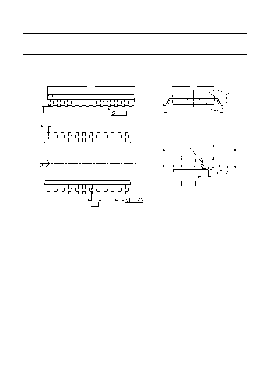
PACKAGE OUTLINE
handbook, full pagewidth
7.6
7.4
10.65
10.00
A
MBC235 - 1
0.3
0.1
2.45
2.25
1.1
0.5
0.32
0.23
1.1
1.0
0 to 8
o
2.65
2.35
detail A
S
15.6
15.2
0.1 S
1
12
13
24
pin 1
index
0.9
0.4
(4x)
0.25 M
(24x)
0.49
0.36
1.27
Fig.9 Plastic small outline package; 24 leads; body width 7.5 mm (SO24; SOT137-1).
Dimensions in mm.

December 1994
19
Philips Semiconductors
Objective specification
Battery charge level indicator
SAA1501T
SOLDERING
Plastic small-outline packages
B
Y WAVE
During placement and before soldering, the component
must be fixed with a droplet of adhesive. After curing the
adhesive, the component can be soldered. The adhesive
can be applied by screen printing, pin transfer or syringe
dispensing.
Maximum permissible solder temperature is 260
∞
C, and
maximum duration of package immersion in solder bath is
10 s, if allowed to cool to less than 150
∞
C within 6 s.
Typical dwell time is 4 s at 250
∞
C.
A modified wave soldering technique is recommended
using two solder waves (dual-wave), in which a turbulent
wave with high upward pressure is followed by a smooth
laminar wave. Using a mildly-activated flux eliminates the
need for removal of corrosive residues in most
applications.
B
Y SOLDER PASTE REFLOW
Reflow soldering requires the solder paste (a suspension
of fine solder particles, flux and binding agent) to be
applied to the substrate by screen printing, stencilling or
pressure-syringe dispensing before device placement.
Several techniques exist for reflowing; for example,
thermal conduction by heated belt, infrared, and
vapour-phase reflow. Dwell times vary between 50 and
300 s according to method. Typical reflow temperatures
range from 215 to 250
∞
C.
Preheating is necessary to dry the paste and evaporate
the binding agent. Preheating duration: 45 min at 45
∞
C.
R
EPAIRING SOLDERED JOINTS
(
BY HAND
-
HELD SOLDERING
IRON OR PULSE
-
HEATED SOLDER TOOL
)
Fix the component by first soldering two, diagonally
opposite, end pins. Apply the heating tool to the flat part of
the pin only. Contact time must be limited to 10 s at up to
300
∞
C. When using proper tools, all other pins can be
soldered in one operation within 2 to 5 s at between 270
and 320
∞
C. (Pulse-heated soldering is not recommended
for SO packages.)
For pulse-heated solder tool (resistance) soldering of VSO
packages, solder is applied to the substrate by dipping or
by an extra thick tin/lead plating before package
placement.
DEFINITIONS
LIFE SUPPORT APPLICATIONS
These products are not designed for use in life support appliances, devices, or systems where malfunction of these
products can reasonably be expected to result in personal injury. Philips customers using or selling these products for
use in such applications do so at their own risk and agree to fully indemnify Philips for any damages resulting from such
improper use or sale.
Data sheet status
Objective specification
This data sheet contains target or goal specifications for product development.
Preliminary specification
This data sheet contains preliminary data; supplementary data may be published later.
Product specification
This data sheet contains final product specifications.
Limiting values
Limiting values given are in accordance with the Absolute Maximum Rating System (IEC 134). Stress above one or
more of the limiting values may cause permanent damage to the device. These are stress ratings only and operation
of the device at these or at any other conditions above those given in the Characteristics sections of the specification
is not implied. Exposure to limiting values for extended periods may affect device reliability.
Application information
Where application information is given, it is advisory and does not form part of the specification.

Philips Semiconductors
Philips Semiconductors ≠ a worldwide company
Argentina: IEROD, Av. Juramento 1992 - 14.b, (1428)
BUENOS AIRES, Tel. (541)786 7633, Fax. (541)786 9367
Australia: 34 Waterloo Road, NORTH RYDE, NSW 2113,
Tel. (02)805 4455, Fax. (02)805 4466
Austria: Triester Str. 64, A-1101 WIEN, P.O. Box 213,
Tel. (01)60 101-1236, Fax. (01)60 101-1211
Belgium: Postbus 90050, 5600 PB EINDHOVEN, The Netherlands,
Tel. (31)40 783 749, Fax. (31)40 788 399
Brazil: Rua do Rocio 220 - 5
th
floor, Suite 51,
CEP: 04552-903-S√O PAULO-SP, Brazil.
P.O. Box 7383 (01064-970).
Tel. (011)821-2333, Fax. (011)829-1849
Canada: PHILIPS SEMICONDUCTORS/COMPONENTS:
Tel. (800) 234-7381, Fax. (708) 296-8556
Chile: Av. Santa Maria 0760, SANTIAGO,
Tel. (02)773 816, Fax. (02)777 6730
Colombia: IPRELENSO LTDA, Carrera 21 No. 56-17,
77621 BOGOTA, Tel. (571)249 7624/(571)217 4609,
Fax. (571)217 4549
Denmark: Prags Boulevard 80, PB 1919, DK-2300 COPENHAGEN S,
Tel. (032)88 2636, Fax. (031)57 1949
Finland: Sinikalliontie 3, FIN-02630 ESPOO,
Tel. (9)0-50261, Fax. (9)0-520971
France: 4 Rue du Port-aux-Vins, BP317,
92156 SURESNES Cedex,
Tel. (01)4099 6161, Fax. (01)4099 6427
Germany: P.O. Box 10 63 23, 20043 HAMBURG,
Tel. (040)3296-0, Fax. (040)3296 213.
Greece: No. 15, 25th March Street, GR 17778 TAVROS,
Tel. (01)4894 339/4894 911, Fax. (01)4814 240
Hong Kong: PHILIPS HONG KONG Ltd., 6/F Philips Ind. Bldg.,
24-28 Kung Yip St., KWAI CHUNG, N.T.,
Tel. (852)424 5121, Fax. (852)428 6729
India: Philips INDIA Ltd, Shivsagar Estate, A Block ,
Dr. Annie Besant Rd. Worli, Bombay 400 018
Tel. (022)4938 541, Fax. (022)4938 722
Indonesia: Philips House, Jalan H.R. Rasuna Said Kav. 3-4,
P.O. Box 4252, JAKARTA 12950,
Tel. (021)5201 122, Fax. (021)5205 189
Ireland: Newstead, Clonskeagh, DUBLIN 14,
Tel. (01)640 000, Fax. (01)640 200
Italy: PHILIPS SEMICONDUCTORS S.r.l.,
Piazza IV Novembre 3, 20124 MILANO,
Tel. (0039)2 6752 2531, Fax. (0039)2 6752 2557
Japan: Philips Bldg 13-37, Kohnan 2 -chome, Minato-ku, TOKYO 108,
Tel. (03)3740 5028, Fax. (03)3740 0580
Korea: (Republic of) Philips House, 260-199 Itaewon-dong,
Yongsan-ku, SEOUL, Tel. (02)794-5011, Fax. (02)798-8022
Malaysia: No. 76 Jalan Universiti, 46200 PETALING JAYA,
SELANGOR, Tel. (03)750 5214, Fax. (03)757 4880
Mexico: 5900 Gateway East, Suite 200, EL PASO, TX 79905,
Tel. 9-5(800)234-7381, Fax. (708)296-8556
Netherlands: Postbus 90050, 5600 PB EINDHOVEN, Bldg. VB
Tel. (040)783749, Fax. (040)788399
New Zealand: 2 Wagener Place, C.P.O. Box 1041, AUCKLAND,
Tel. (09)849-4160, Fax. (09)849-7811
Norway: Box 1, Manglerud 0612, OSLO,
Tel. (022)74 8000, Fax. (022)74 8341
Pakistan: Philips Electrical Industries of Pakistan Ltd.,
Exchange Bldg. ST-2/A, Block 9, KDA Scheme 5, Clifton,
KARACHI 75600, Tel. (021)587 4641-49,
Fax. (021)577035/5874546.
Philippines: PHILIPS SEMICONDUCTORS PHILIPPINES Inc,
106 Valero St. Salcedo Village, P.O. Box 2108 MCC, MAKATI,
Metro MANILA, Tel. (02)810 0161, Fax. (02)817 3474
Portugal: PHILIPS PORTUGUESA, S.A.,
Rua dr. AntÛnio Loureiro Borges 5, Arquiparque - Miraflores,
Apartado 300, 2795 LINDA-A-VELHA,
Tel. (01)4163160/4163333, Fax. (01)4163174/4163366.
Singapore: Lorong 1, Toa Payoh, SINGAPORE 1231,
Tel. (65)350 2000, Fax. (65)251 6500
South Africa: S.A. PHILIPS Pty Ltd.,
195-215 Main Road Martindale, 2092 JOHANNESBURG,
P.O. Box 7430 Johannesburg 2000,
Tel. (011)470-5911, Fax. (011)470-5494.
Spain: Balmes 22, 08007 BARCELONA,
Tel. (03)301 6312, Fax. (03)301 42 43
Sweden: Kottbygatan 7, Akalla. S-164 85 STOCKHOLM,
Tel. (0)8-632 2000, Fax. (0)8-632 2745
Switzerland: Allmendstrasse 140, CH-8027 ZÐRICH,
Tel. (01)488 2211, Fax. (01)481 77 30
Taiwan: PHILIPS TAIWAN Ltd., 23-30F, 66, Chung Hsiao West
Road, Sec. 1. Taipeh, Taiwan ROC, P.O. Box 22978,
TAIPEI 100, Tel. (02)388 7666, Fax. (02)382 4382.
Thailand: PHILIPS ELECTRONICS (THAILAND) Ltd.,
209/2 Sanpavuth-Bangna Road Prakanong,
Bangkok 10260, THAILAND,
Tel. (662)398-0141, Fax. (662)398-3319.
Turkey: Talatpasa Cad. No. 5, 80640 GÐLTEPE/ISTANBUL,
Tel. (0 212)279 2770, Fax. (0212)269 3094
United Kingdom: Philips Semiconductors LTD.,
276 Bath road, Hayes, MIDDLESEX UB3 5BX,
Tel. (081)73050000, Fax. (081)7548421
United States: 811 East Arques Avenue, SUNNYVALE,
CA 94088-3409, Tel. (800)234-7381, Fax. (708)296-8556
Uruguay: Coronel Mora 433, MONTEVIDEO,
Tel. (02)70-4044, Fax. (02)92 0601
For all other countries apply to: Philips Semiconductors,
International Marketing and Sales, Building BE-p,
P.O. Box 218, 5600 MD, EINDHOVEN, The Netherlands,
Telex 35000 phtcnl, Fax. +31-40-724825
SCD35
© Philips Electronics N.V. 1994
All rights are reserved. Reproduction in whole or in part is prohibited without the
prior written consent of the copyright owner.
The information presented in this document does not form part of any quotation
or contract, is believed to be accurate and reliable and may be changed without
notice. No liability will be accepted by the publisher for any consequence of its
use. Publication thereof does not convey nor imply any license under patent- or
other industrial or intellectual property rights.
Printed in The Netherlands
373061/1500/01/pp20
Date of release: December 1994
Document order number:
9397 743 50011