 | –≠–ª–µ–∫—Ç—Ä–æ–Ω–Ω—ã–π –∫–æ–º–ø–æ–Ω–µ–Ω—Ç: SAA2013 | –°–∫–∞—á–∞—Ç—å:  PDF PDF  ZIP ZIP |
Document Outline
- FEATURES
- GENERAL DESCRIPTION
- ORDERING INFORMATION
- BLOCK DIAGRAM
- PINNING
- FUNCTIONAL DESCRIPTION
- PASC processor
- Decode/encode control
- Reset
- Sleep mode
- Low-power decode mode
- Power-On Reset (POR)
- Encode mode
- Decode mode
- Filtered data interface
- Audio sample resolution section
- Control interfaces
- SAA2013 interface modes
- Current consumption
- LIMITING VALUES
- CHARACTERISTICS
- PACKAGE OUTLINE
- SOLDERING
- DEFINITIONS
- LIFE SUPPORT APPLICATIONS

DATA SHEET
Preliminary specification
File under Integrated Circuits, IC01
May 1994
INTEGRATED CIRCUITS
Philips Semiconductors
SAA2013
Adaptive allocation and scaling for
PASC coding in DCC systems
May 1994
2
Philips Semiconductors
Preliminary specification
Adaptive allocation and scaling for PASC
coding in DCC systems
SAA2013
FEATURES
∑
Wide operating voltage range: 2.7 to 5.5 V
∑
Low power consumption: 13 mW; 3.0 V
∑
Low power decode mode: 1 mW; 5.0 V
∑
Sleep mode for low power and low Electromagnetic
Interference (EMI)
∑
Sophisticated allocation algorithm
∑
Optimum sound quality
∑
Three-wire L3 bus microcontroller interface
∑
Stereo or 2-channel mono recording
∑
Small surface mounted package (QFP; SOT307).
GENERAL DESCRIPTION
The SAA2013 performs the adaptive allocation and
scaling function in the Precision Adaptive Sub-band
Coding (PASC) system. It is not required in playback only
applications, and is only used during recording. To
complete the PASC processor, a SAA2003 stereo filter
and codec is required.
ORDERING INFORMATION
Note
1. When using reflow soldering it is recommended that the Dry Packing instructions in the
"Quality Reference
Pocketbook" are followed. The pocketbook can be ordered using the code 9398 510 34011.
TYPE NUMBER
PACKAGE
PINS
PIN POSITION
MATERIAL
CODE
SAA2013H
44
QFP
(1)
plastic
SOT307-2
May 1994
3
Philips Semiconductors
Preliminary specification
Adaptive allocation and scaling for PASC
coding in DCC systems
SAA2013
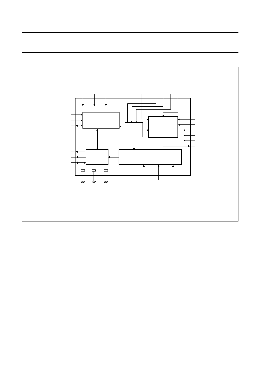
BLOCK DIAGRAM
Fig.1 Block diagram.
handbook, full pagewidth
MGB355
VDD2
VDD1
VDD3
14
24
40
6
25
44
SAA2013
MICROCONTROLLER
BUS
3
4
5
L3MODEM
L3CLKM
L3DATAM
CONTROL
AND
SYNC
COMPENSATION
DELAY
39
SFC
BUS
ALLOCATION AND SCALE FACTOR
COMPUTATION
37
36
35
34
FS256
FDIR
FRESET
FSYNC
FDAI
32
31
30
26
33
9
10
11
L3MODEC
L3CLKC
L3DATAC
22
21
20
NODONE
RESOL0
RESOL1
VSS2
VSS1
VSS3
FDCL
FDWS
SLEEP
CLK24
23
RESET
FDAO

May 1994
4
Philips Semiconductors
Preliminary specification
Adaptive allocation and scaling for PASC
coding in DCC systems
SAA2013
PINNING
SYMBOL
PIN
DESCRIPTION
TYPE
TEST10
1
test input; connect to V
SS
I
TEST11
2
test input; connect to V
SS
I
L3MODEM
3
microcontroller interface mode input
I
L3CLKM
4
microcontroller interface clock input
I
L3DATAM
5
microcontroller interface data 3-state input/output
I/O
V
SS1
6
supply ground
-
TEST12
7
test output; do not connect
O
TEST13
8
test output; do not connect
O
L3MODEC
9
codec interface mode output
O
L3CLKC
10
codec interface clock output
O
L3DATAC
11
codec interface data 3-state input/output
I/O
TEST1
12
test output; do not connect
O
TEST2
13
test output; do not connect
O
V
DD1
14
supply voltage
-
TEST3
15
test mode input; connect to V
DD
I
TEST4
16
test mode input; connect to V
DD
I
TEST5
17
test input; connect to V
SS
I
TEST6
18
test input; connect to V
SS
I
TEST7
19
test input; connect to V
SS
I
NODONE
20
nodone state selection input; connect to V
DD
I
RESOL0
21
resolution selection 0 input
I
RESOL1
22
resolution selection 1 input
I
RESET
23
reset input; active HIGH
I
V
DD2
24
supply voltage
-
V
SS2
25
supply ground
-
CLK24
26
24.576 MHz clock input
I
LOWPWR
27
low power decode select input
I
POR
28
power on reset input
I
TEST8
29
test input; connect to V
SS
I
SLEEP
30
sleep mode select input
I
FDWS
31
filtered data word select
I
FDCL
32
filtered data clock
I
FDAO
33
filtered data output
O
FDAI
34
filtered data input
I
FSYNC
35
sub-band synchronization on filtered I
2
S bus
I
FRESET
36
reset signal input from SAA2003
I
FDIR
37
filtered data direction input
I
TEST9
38
test input; connect to V
SS
I
FS256
39
system clock input; 256
◊
sample frequency (f
s
)
I
V
DD3
40
supply voltage
-

May 1994
5
Philips Semiconductors
Preliminary specification
Adaptive allocation and scaling for PASC
coding in DCC systems
SAA2013
n.c.
41
not connected
-
n.c.
42
not connected
-
n.c.
43
not connected
-
V
SS3
44
supply ground
-
SYMBOL
PIN
DESCRIPTION
TYPE
Fig.2 Pin configuration.
handbook, full pagewidth
1
2
3
4
5
6
7
8
9
10
11
33
32
31
30
29
28
27
26
25
24
23
12
13
14
15
16
17
18
19
20
21
22
44
43
42
41
40
39
38
37
36
35
34
FDAO
FDCL
FDWS
SLEEP
TEST8
V
CLK24
RESET
SS2
VDD2
n.c.
n.c.
n.c.
SS3
DD1
TEST9
FDIR
FRESET
FSYNC
FDAI
V
V
TEST10
TEST11
L3MODEM
L3CLKM
L3DATAM
L3MODEC
L3CLKC
L3DATAC
SAA2013
TEST1
RESOL0
RESOL1
MGB356
SS1
V
TEST12
TEST13
POR
LOWPWR
FS256
TEST2
TEST7
TEST6
NODONE
TEST5
TEST4
TEST3
DD3
V
May 1994
6
Philips Semiconductors
Preliminary specification
Adaptive allocation and scaling for P
ASC
coding in DCC systems
SAA2013
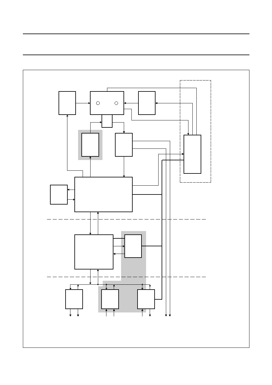
FUNCTIONAL DESCRIPTION
handbook, full pagewidth
MBD620
TAPE DRIVE PROCESSING
DAC
TDA1305
ADC
SAA7366
analog
output
DIGITAL
AUDIO I/O
TDA1315
IEC958
analog
input
AUDIO IN/OUT
PASC PROCESSOR
I S
2
L
R
L
R
SFC3
SAA2003
STEREO
FILTER CODEC
ADAS3
SAA2013
ADAPTIVE
ALLOCATION
filtered I S
2
sub-band
I S
2
baseband
DRP
SAA2023
OR
SAA3323
DRIVE
PROCESSOR
RAM
41464
BUFFER
64K x 4
RDAMP
TDA1380
READ AMP.
WRAMP
TDA1381
WRITE AMP.
FIXED
HEAD
TAPE
CAPSTAN
DRIVE
speed control
MECHANICS
DRIVERS
analog CC
L output
analog CC
R output
SYSTEM
MICROCONTROLLER
SYSTEM CONTROL
search data
detect
switch
Fig.3 DCC system block diagram.
May 1994
7
Philips Semiconductors
Preliminary specification
Adaptive allocation and scaling for PASC
coding in DCC systems
SAA2013
PASC processor
The PASC processor is a dedicated Digital Signal
Processor (DSP) engine which efficiently codes digital
audio data at a bit rate of 384 kbits/s without affecting the
sound quality. This is achieved using an efficient adaptive
data notation and by only encoding the audio information
which can be heard by the human ear.
The audio data is split into 32 equal sub-bands during
encoding. For each of the sub-bands a masking threshold
is calculated. The samples from each of the sub-bands are
included in the PASC data with an accuracy that is
determined by the available bit-pool and by the difference
between the signal power and the masking threshold for
that sub-band. In decode, the sub-band signals are
reconstructed into the full bandwidth audio signal.
The stereo filter codec performs the splitting (encoding)
and reconstruction (decoding), including the necessary
formatting functions. During encoding, the adaptive
allocation and scaling circuit calculates the required
accuracy (bit allocation) and scale factors of the
sub-band samples.
Decode/encode control
Selection of decode or encode is controlled using FRESET
and FDIR. FRESET causes a general reset. The FDIR
signal is sampled at the falling edge of the FRESET signal
to determine the operation mode. When FDIR is HIGH,
SAA2013 is in decode mode. When FDIR is LOW the
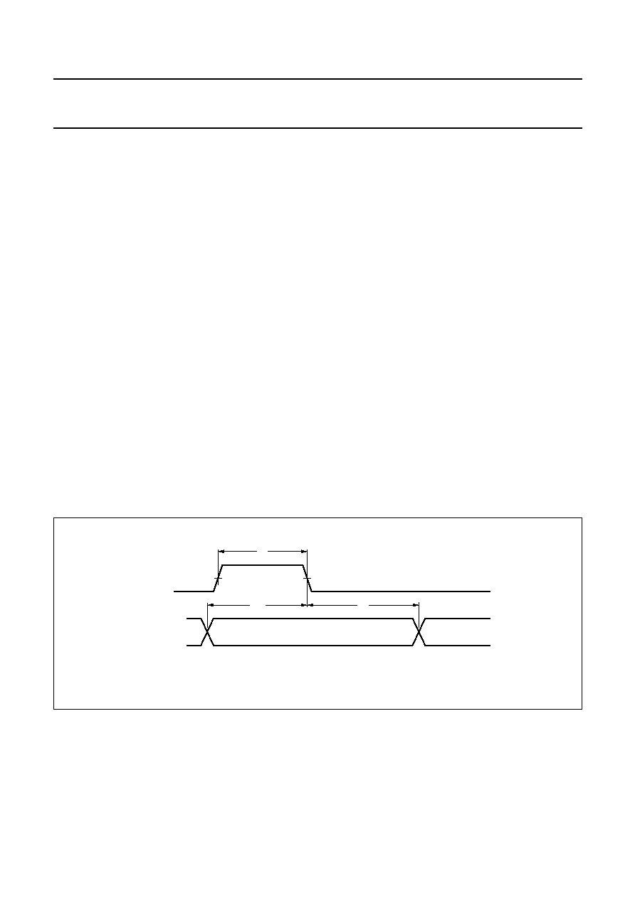
SAA2013 is in encode mode. See Fig.4.
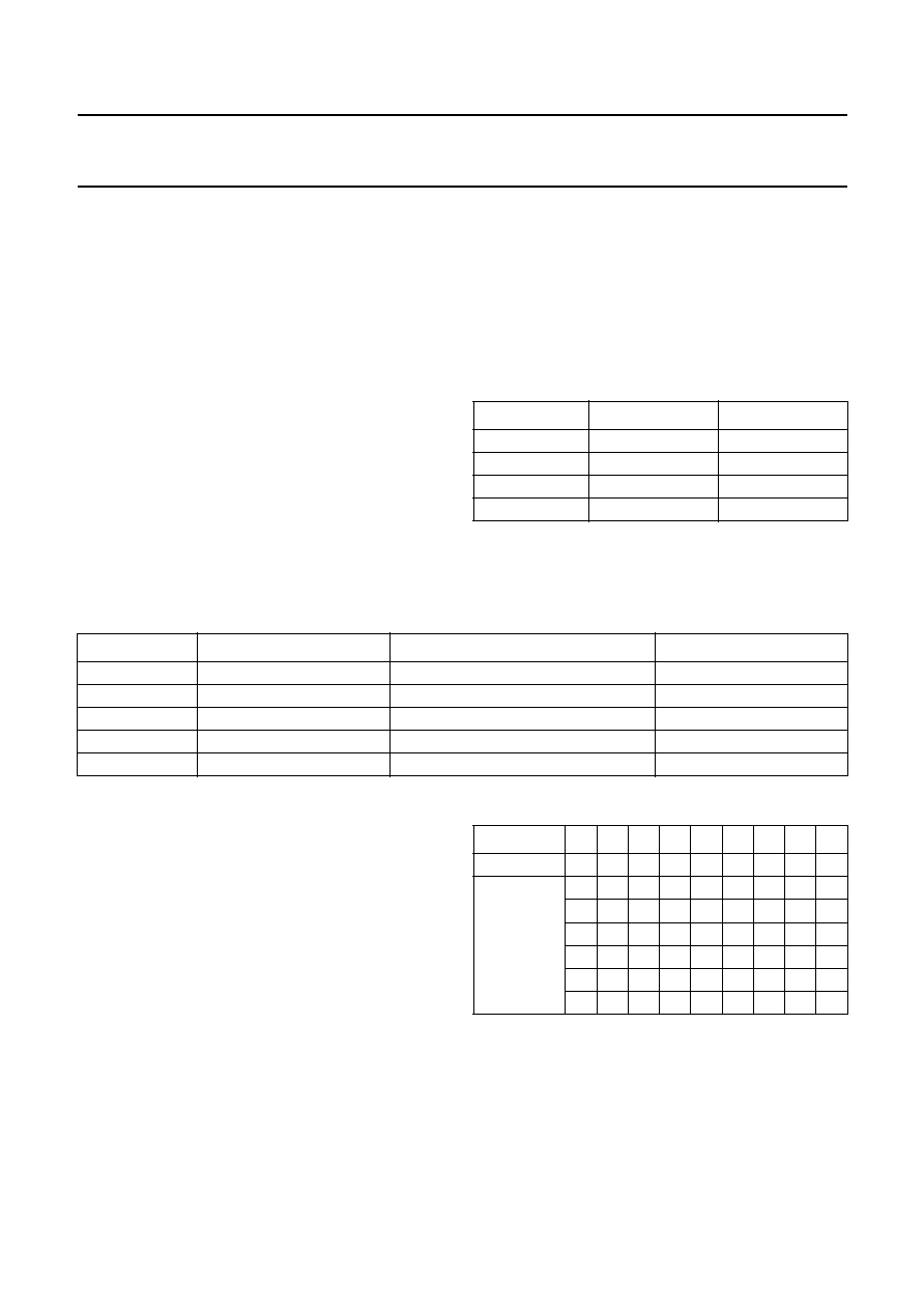
Fig.4 FDIR and FRESET timing.
handbook, full pagewidth
tH
FRESET
FDIR
t su
t h
MGB357
Reset
When used with low-power mode disabled
(LOWPWR = V
SS
), and with the SLEEP input LOW,
SAA2013 is reset if the RESET pin is held HIGH for at least
5 periods of the CLK24 clock, see Fig.5. SAA2013 defaults
to decode mode. When in low-power mode, the RESET
pin is disabled.
Sleep mode
Sleep mode is entered by taking the SLEEP input HIGH
with the LOWPWR pin connected to V
SS
; CLK24 and
FS256 are stopped internally to the SAA2013, the 3-state
buffers will have a high impedance, and outputs will freeze
in the same state as just before the sleep mode became
active (clocks stopped). To come out of sleep mode, the
SLEEP input must be taken LOW again. To clear data
present from before sleep was entered, this should be
followed by a reset, see Fig.5.

May 1994
8
Philips Semiconductors
Preliminary specification
Adaptive allocation and scaling for PASC
coding in DCC systems
SAA2013
Fig.5 SLEEP and RESET timing.
handbook, full pagewidth
MGB358
t d
t h
SLEEP
RESET
CLK24
Low-power decode mode
Low-power decode mode is made available by connecting
the LOWPWR pin to V
DD
. With LOWPWR = V
DD
,
low-power decode mode is entered 9 cycles of CLK24
after the SLEEP input is taken HIGH. In low-power decode
mode, the L3 bus connections are connected straight
trough the SAA2013, which is effectively bypassed. The
compensation delay connection between pins FDAI and
FDAO is no longer needed by the SAA2003, and CLK24
and FS256 are stopped internally to the SAA2013.
To get out of low-power decode mode, it is necessary to
take SLEEP LOW, FDIR LOW, and FRESET HIGH (in a
normal application taking FDIR LOW and FRESET HIGH
can be achieved by setting SAA2003 into encode mode),
SAA2013 then performs an internal reset, and defaults to
normal decode mode. The RESET pin does not reset the
circuit from low-power decode mode.
Power-On Reset (POR)
When low-power decode mode is enabled
(LOWPWR = V
DD
), a power-on reset circuit is required to
ensure that the internal clocks are connected correctly at
power-on. A suitable circuit is shown in Fig.6. This circuit
will correctly reset the internal clock connection provided
that the nominal value of the V
DD
supply is reached within
40 ms at power-on.
Encode mode
In encode mode the SAA2013 receives sub-band filtered
samples from SAA2003 on the FDAI pin. The SAA2013
has to collect a complete frame of sub-band data before
the allocation and scale factor information can be
calculated. So that the allocation and scale factor
information is available in the same time frame as the
audio samples at the output, the sub-band filtered samples
are delayed by 480 FDWS periods.
One FDWS period is equal to
where f
s
is the audio
sample rate of 32, 44.1 or 48 kHz. The delayed samples
are passed to the codec part of SAA2003 on the
FDAO pin.
handbook, halfpage
MGB359
V
DD
150
k
µ
1 F
POR
VSS
V
DD
V
SS
Fig.6 POR circuit.
1
f
s
----
May 1994
9
Philips Semiconductors
Preliminary specification
Adaptive allocation and scaling for PASC
coding in DCC systems
SAA2013
For each sub-band frame, SAA2013 calculates the
allocation and scale factor index information required by
the SAA2003. In order to synchronize the codec part of
SAA2003, SAA2013 frequently requests status
information from the codec. It monitors sample frequency,
emphasis information and stereo mode, and uses the
ready-to-receive bit of the codec to determine when to
transfer information.
Decode mode
In decode the SAA2003 will transfer samples from FDAI to
FDAO with a delay of 480 FDWS periods. Settings and
status information can be sent to SAA2003 via SAA2013,
but the SAA2013 does not itself act on this information.
Transfer of this information is automatically synchronized
to the ready-to-receive bit of SAA2003 by SAA2013.
Audio sample resolution section
The SAA2013 is designed for operation with audio input
sources of 14, 15, 16 or 18-bit resolution.
For optimum audio performance the bit allocation
algorithm of the SAA2013 can be varied to suit the bit
resolution of the audio source. This is done with the pins
RESOL0 and RESOL1 as shown in Table 1.
Table 1
Resolution set by pins RESOL0 and RESOL1.
RESOLUTION
RESOL0
RESOL1
16 bits
0
0
18 bits
0
1
14 bits
1
0
15 bits
1
1
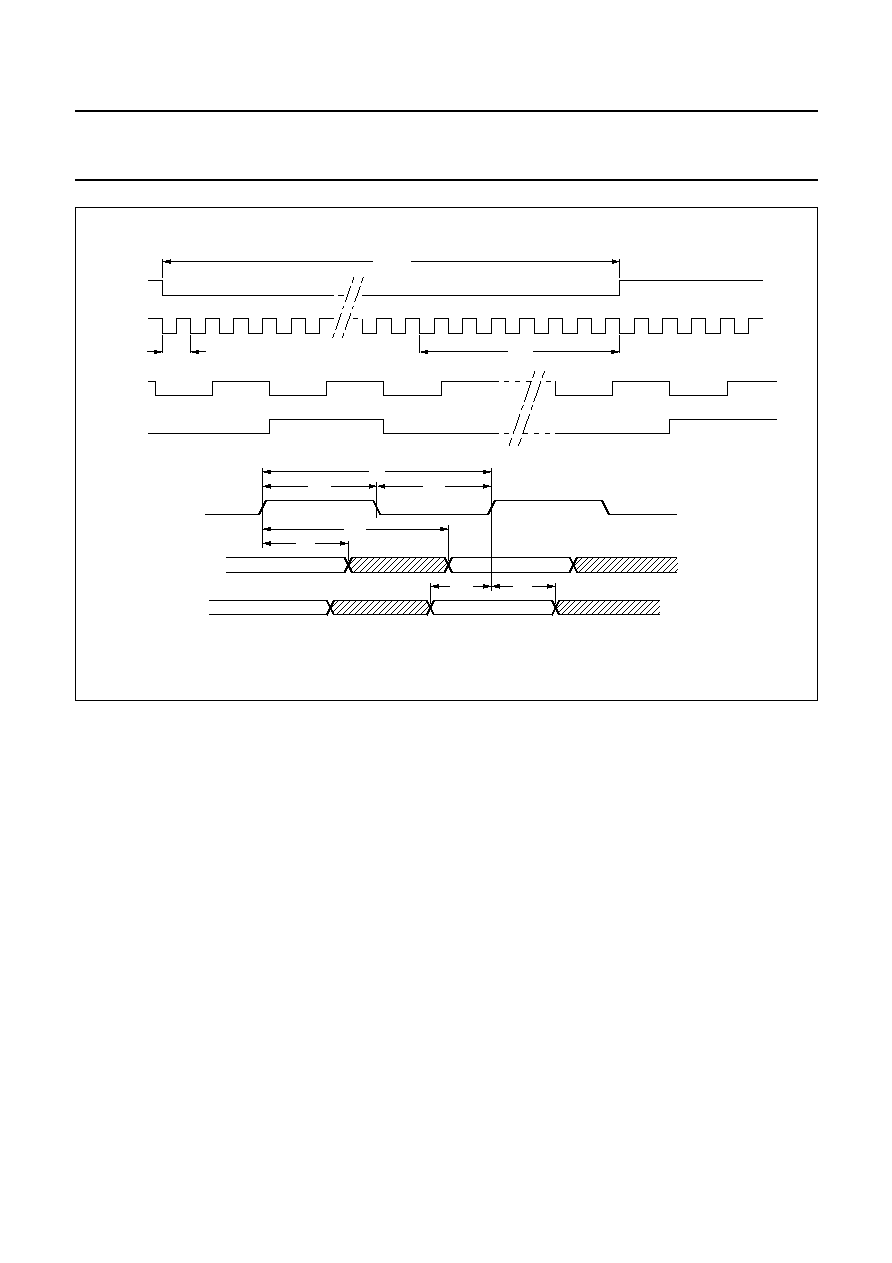
Filtered data interface
The filtered data interface signals are given in Table 2.
Table 2
Filtered data interface signals.
PIN
INPUT/OUTPUT
FUNCTION
FREQUENCY
FDWS
input
filtered data interface word select
f
s
FDCL
input
filtered data interface bit clock
64f
s
FDAI
input
filtered data input
-
FDAO
output
filtered data output
-
FSYNC
input
filtered data sub-band synchronization
-
The filtered data interface transfers sub-band filtered
samples between the stereo filter codec SAA2003 and
SAA2013. The interface is similar to a normal I
2
S interface,
consisting of clock (FDCL), data (FDAI/FDAO) and word
select lines (FDWS), except that the samples sent
represent signals divided into 32 sub-bands. One frame of
data consists of 12 samples from 32 sub-bands for both
left and right channels, i.e.: 768 audio samples. Each
audio sub-band sample is represented by a 24-bit two's
complement number.
The order in which the samples are sent is shown in
Table 3.
For two channel mono, the order is the same, but with
Channel 1 samples in the place of left and Channel 2
samples in place of right.
Table 3
Order of samples.
The signal FSYNC is used between each PASC frame to
indicate the sending of samples for sub-band 0 (Fig.7).
SUB-BAND
0
0
1
1
2
2
...
31
31
Channel
L
R
L
R
L
R
...
L
R
Sample
0
0
0
0
0
0
...
0
0
1
1
1
1
1
1
...
1
1
2
2
2
2
2
2
...
2
2
.
.
.
.
.
.
...
.
.
.
.
.
.
.
.
...
.
.
11
11
11
11
11
11
...
11
11
May 1994
10
Philips Semiconductors
Preliminary specification
Adaptive allocation and scaling for PASC
coding in DCC systems
SAA2013
Fig.7 Filtered interface format.
handbook, full pagewidth
left
right
L
R
L
R
L
R
L
R
L
R
31
0
1
31
0
32 bits
t d3
cL
t
cH
t
t d4
Tc
t su1
t h1
FDCL
FDAO
FDAI
FDWS
FSYNC
sub-band
FDWS
FDCL
FDWS
channel
FSYNC
timing
MGB360
1 bit
23
22
21
20
7 bit
0
1
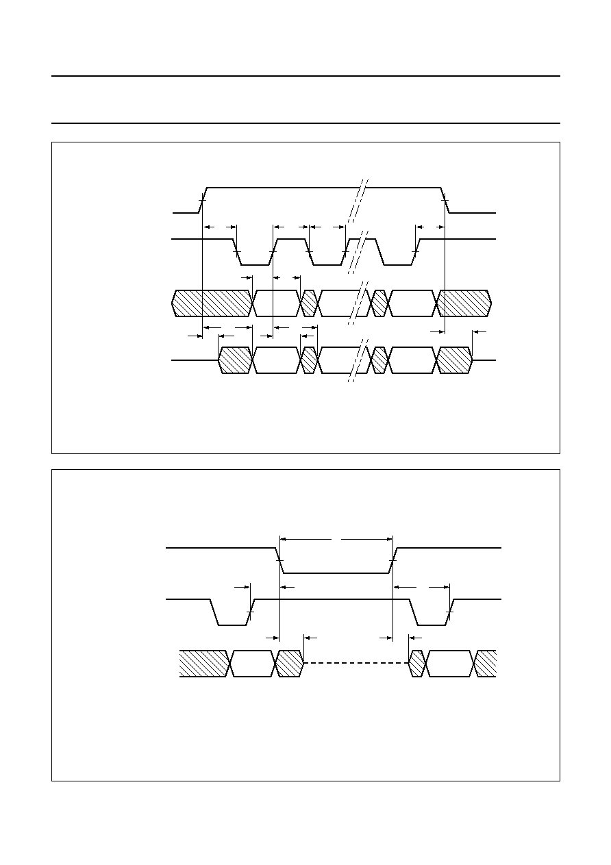
Control interfaces
Two 3-wire control interfaces are provided (referred to as
`L3' interfaces). One is connected to the system
microcontroller (L3MODEM, L3CLKM, L3DATAM where
`M' represents microcontroller), the other to SAA2003
(L3MODEC, L3CLKC, L3DATAC where `C' represents
codec). In general, control data is passed between
SAA2003 and the microcontroller via SAA2013. This
ensures that the microcontroller is buffered from the
time-critical SAA2013 to SAA2003 interface during
encode.
The SAA2013 does not interpret the data from the
microcontroller interface.
Status information from the codec is interpreted to ensure
that SAA2013 quickly acts upon the status of SAA2003.
The L3 bus operation is shown in Fig.8. There are three
modes:
1. Address.
2. Data.
3. Halt.
Each interface operates as either a master or a slave,
where the master provides L3CLK and L3MODE. For the
microcontroller to SAA2013 interface, the microcontroller
is the master. For the SAA2013 to SAA2003 interface,
SAA2013 is the master.

May 1994
11
Philips Semiconductors
Preliminary specification
Adaptive allocation and scaling for PASC
coding in DCC systems
SAA2013
handbook, full pagewidth
L3MODE
L3CLK
L3DATA
0
1
2
3
4
5
6
7
MGB361
Fig.8 L3 bus operation; address mode.
handbook, full pagewidth
L3MODE
L3CLK
L3DATA
0
1
2
3
4
5
6
7
MGB362
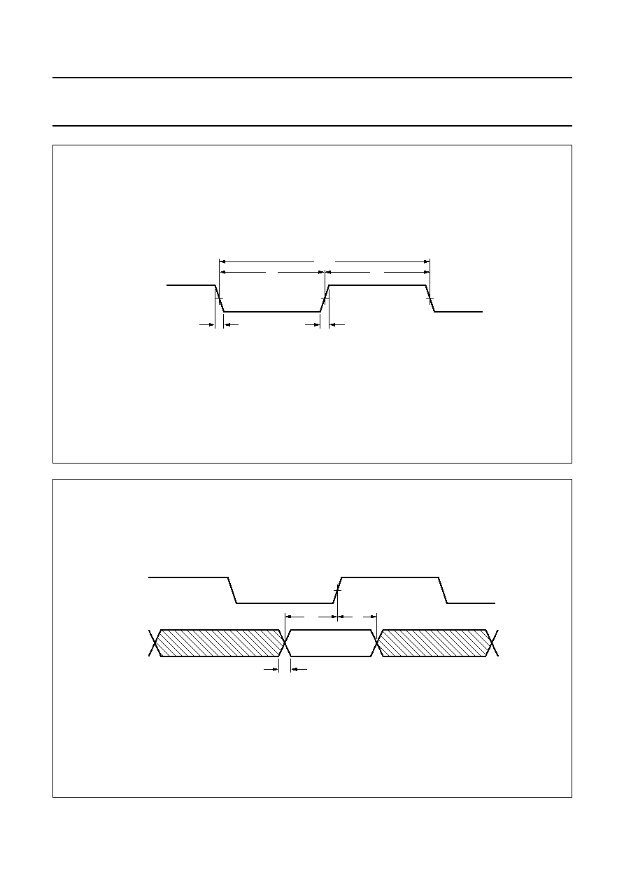
Fig.9 L3 single byte transfer.
handbook, full pagewidth
L3MODE
L3CLK
L3DATA
8
9
10 11 12 13 14 15
MGB363
0
1
2
3
4
5
6
7
Fig.10 L3 bus two byte transfer.

May 1994
12
Philips Semiconductors
Preliminary specification
Adaptive allocation and scaling for PASC
coding in DCC systems
SAA2013
A
DDRESS MODE
Address mode is entered by the master pulling L3MODE
LOW. This causes the L3DATA line to act as an input on
the slave, and 8 bits of address data are clocked into the
slave. If the slave recognizes the address, it will set-up its
internal state based on the 2 Least Significant Bits (LSBs)
of the address. The slave than expects to send status data
or receive control data.
The addresses for SAA2013 are shown in Table 4.
Table 4
SAA2013 addresses.
The interface may be reset by sending an address of all
zeros (`00000000'). This may be used to allow
inter-operation with other devices sharing the L3CLK and
L3DATA lines (e.g. SAA7345 CD decoder).
D
ATA MODE
In data mode, bytes of data are clocked into (e.g. control)
or out of (e.g. status) the slave. A single byte transfer is
shown in Fig.9. A two byte transfer is shown in Fig.10,
between bytes there must be a pause during which the
clock remains HIGH.
MSB
LSB
L3 OPERATION
MODE
FUNCTION
0010
0000
WDAT
extended settings
0010
0001
RDAT
allocation information
0010
0010
WCMD
settings
0010
0011
RSTAT
status/peak read
H
ALT MODE
Halt mode consists of pulling L3MODE LOW after sending
data. It is used for marking the end of a data transfer mode
which does not have an internal bit counter.
SAA2013 interface modes
The SAA2013 may be used to read and write from or to
SAA2003. Information is transferred via a set of transit
registers within SAA2013.
D
ECODE OPERATION
During decode, the SAA2013 does not perform allocation.
Therefore no allocation and scale factor indices are sent to
SAA2003. Settings and extended settings may still be sent
to SAA2003, and SAA2013 monitors the status of the
codec by reading status from it after every occurrence of
FSYNC. Peak level data can also be transferred from
SAA2003.
E
NCODE OPERATION
In encode, the same information may be sent as for
decode, and in addition, allocation/scale factor indices are
sent to the codec by SAA2013.
The interface modes are shown in Table 5.

May 1994
13
Philips Semiconductors
Preliminary specification
Adaptive allocation and scaling for PASC
coding in DCC systems
SAA2013
Table 5
Interface modes.
MODE
ADDRESS
INTERFACE MODE
LENGTH (BITS)
DIRECTION
BIT 1
BIT 0
Decode
0
0
extended settings
8
microcontroller to SAA2003
0
1
-
-
-
1
0
settings
16
microcontroller to SAA2003
1
1
status/peak
16 or 48
SAA2003 to microcontroller
Encode
0
0
extended settings
8
microcontroller to SAA2003
0
1
allocation/scale
48
◊
16
SAA2013 to SAA2003
1
0
settings
16
microcontroller to SAA2003
1
1
status/peak
16 or 48
SAA2003 to microcontroller
P
RIORITY
Each type of transfer has a priority. The priorities are:
1. Allocation/scale/settings (highest priority).
2. Status read.
3. Peak read.
4. Extended settings (lowest priority).
A
LLOCATION AND SCALE FACTOR TRANSFER
The allocation and scale factor information sent from
SAA2013 to SAA2003 during encode has the highest
priority. The other types of transfer interleaved with the
allocation/scale information.
S
ETTINGS TRANSFER
This is a 16-bit transfer. The microcontroller sends settings
to SAA2003. SAA2013 only transfers these without taking
notice of the contents. In encode, the settings are held in
the transit registers, and sent next time that allocation is
being sent. In decode, settings are sent as soon as
possible subject to the RTRC flag from SAA2003.
Before sending settings the microcontroller should read
the status of SAA2013 to examine the Ready-To-Receive
bit Settings (RTRS). After the settings have been received
by SAA2013, RTRS will be made logic 0, until the settings
have been sent to SAA2003. Only after RTRS is logic 1
again may the microcontroller send new settings.
S
TATUS READ
Status and peak information may be read from SAA2003
by the microcontroller. The status bits are defined in
Table 6.
Table 6
Status bits.
BIT
NAME
FUNCTION
VALID IN
B15 to B12
bit rate index
bit rate indication
encode/decode
B11 and B10
sample frequency indication
44.1, 48, 32 kHz indication
encode/decode
B9
RTRS (settings)
1 = ready; 0 = not ready
encode/decode
B8
RTRE (external settings)
1 = ready; 0 = not ready
encode/decode
B7 and B6
MODE
sub-band signal mode
identification
encode/decode
B5
SYNC
synchronization indication
encode/decode
B4
CLKOK
1 = OK; 0 = not OK
encode/decode
B3 and B2
Tr0 and Tr1
transparent bits
encode/decode
B1 and B0
EMPHASIS
emphasis indication
encode/decode
May 1994
14
Philips Semiconductors
Preliminary specification
Adaptive allocation and scaling for PASC
coding in DCC systems
SAA2013
Since the two bytes of status information are sampled
separately, the bytes may result from different sub-band
frames.
The only valid bit rate code for the SAA2013 is 1100.
The sample frequency indication is shown in Table 7.
Table 7
Sample frequency indication.
Ready-to-receive S or E indicates whether the SAA2013 is
ready-to-receive new settings or extended settings from
the microcontroller. This should be checked before
sending new information.
For details of the MODE, SYNC, CLKOK and transparent
bits, refer to the
"SAA2003 data sheet".
The emphasis indication can be used to apply the correct
de-emphasis. In encode SAA2013 will correct the
calculated allocation if
50
/
15
µ
s emphasis is applied. When
"CCITT J.17" emphasis is applied, the bit allocation
remains the same as when no emphasis is applied.
The 2 bytes of the status are `sampled' at different
moments. So the information may not result from the same
sub-band frame.
When making repeated status reads (for instance reading
the RTRS/RTRE flags before sending settings or extended
settings), the microcontroller must send an address
before each status read, to ensure that the byte counter in
the interface is reset to logic 0. If this is not done, then the
peak data will be read. Conversely, it is important not to
send a new address after a status read if the peak data is
required.
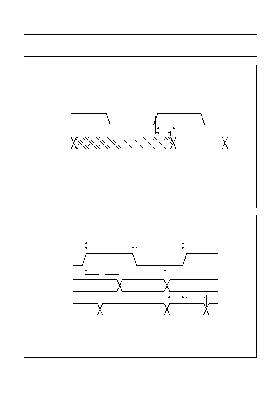
P
EAK READ
Peak information is read by clocking a further 4 bytes of
data after a status read. The data format is shown in
Figs 11 and 12. Bits B17 to B31 contain a 15-bit unsigned
peak, LSB first, channel indicated by bit B16. Bits B33 to
B47 contain a 15-bit unsigned peak, channel indicated by
bit B32.
The peak data is delayed by 1 read period. If for example
the microcontroller reads peak level data every 50 ms, the
peak data sourced by SAA2013 will be 50 ms old. Also it
BIT 11
BIT 10
SAMPLE FREQUENCY
0
0
44.1 kHz; default
0
1
48.0 kHz
1
0
32.0 kHz
1
1
do not use
is possible that peak data may contain an additional delay
of 1 column (667
µ
s minimum at 48 kHz, 1 ms maximum
at 32 kHz). If the microcontroller attempts to read peak
level data with a delay of less than 1 column, the peak level
data from the previous reading will be repeated. Normally
the microcontroller should allow at least 1 ms between
reads. There is also a delay required between peak data
words (Fig.13).
If the SAA2013 does not have peak data available (for
instance the microcontroller attempts two reads in very
quick succession), it will return all peak data bits set to
logic 0. The microcontroller can detect if valid peak data
has been returned by inspecting bits T16 and T32. If both
bits are set to logic 0 the data is not valid.
handbook, halfpage
0 0 1 0 0 0 1 1
STATUS MSB
PEAK BYTE 1
PEAK BYTE 3
STATUS LSB
PEAK BYTE 0
PEAK BYTE 2
MSB
LSB
MGB364
Fig.11 Peak level read format; SAA2013 to
microcontroller.
handbook, halfpage
MSB
LSB
16
15-bit peak
channel
indicator
bits 17 to 31
MSB
LSB
32
15-bit peak
channel
indicator
bits 33 to 47
MGB365
Fig.12 Peak level format.

May 1994
15
Philips Semiconductors
Preliminary specification
Adaptive allocation and scaling for PASC
coding in DCC systems
SAA2013
E
XTENDED SETTINGS
This is a single byte transfer, valid during decode and encode. The sequence of operations is:
1. Microcontroller reads status from SAA2013, waiting for the flag RTRE to be set.
2. When RTRE is logic 1, the microcontroller writes address bit 0 is logic 0, bit 1 is logic 0.
3. One byte of extended settings is clocked into the transit register (SAA2013).
4. When it is possible (i.e. subject to RTRC being HIGH, and assuming that allocation or status is not waiting), the byte
is transferred from the transit register to the SAA2003.
handbook, full pagewidth
L3MODEC
MGB366
STATUS
BYTES
PEAK 1
HALT
PEAK 2
15.625 s
µ
Fig.13 Peak data timing.
Fig.14 L3 interface timing; SAA2013 to SAA2003 (address mode).
handbook, full pagewidth
t d3
td4
td5
td2
t h1
L3MODEC
L3CLKC
L3DATAC
(ADAS-SFC)
MGB367
cL
t
cH
t
t d1
t h2
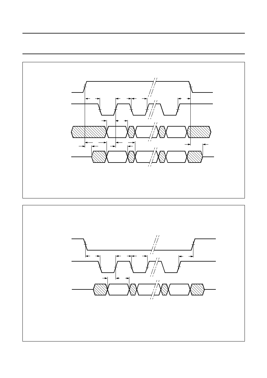
May 1994
16
Philips Semiconductors
Preliminary specification
Adaptive allocation and scaling for PASC
coding in DCC systems
SAA2013
handbook, full pagewidth
td3
td4
t d5
th2
td2
t h3
L3MODEC
L3CLKC
MGB368
cL
t
cH
t
td1
t h1
t su1
L3DATAC
(ADAS-SFC)
L3DATAC
SFC-ADAS)
Fig.15 L3 interface timing; SAA2013 to SAA2003 (data mode).
Fig.16 L3 interface timing; microcontroller to SAA2013 (address mode).
handbook, full pagewidth
L3MODEM
L3CLKM
L3DATAM
(microcontroller-
ADAS)
MGB369
cL
t
cH
t
t d1
t h1
t su1
th2
May 1994
17
Philips Semiconductors
Preliminary specification
Adaptive allocation and scaling for PASC
coding in DCC systems
SAA2013
handbook, full pagewidth
t d3
t d4
t d5
t d2
t h3
L3MODEM
L3CLKCM
MGB370
cL
t
cH
t
t d1
th1
t su1
L3DATAM
(ADAS-
microcontroller)
L3DATAM
(microcontroller-
ADAS)
t h2
Fig.17 L3 interface timing; microcontroller to SAA2013 (data mode).
Fig.18 L3 interface timing; microcontroller to SAA2013 and SAA2013 to SAA2003 (halt mode).
handbook, full pagewidth
L3MODEM/
L3MODEC
L3CLKM/
L3CLKC
L3DATA/
L3DATAC
(OUTPUT)
MGB371
t d5
th2
td2
td1
tL
May 1994
18
Philips Semiconductors
Preliminary specification
Adaptive allocation and scaling for PASC
coding in DCC systems
SAA2013
handbook, full pagewidth
cL
CLK24
t f
t r
t
cH
t
T
MGB372
c24
Fig.19 Input timing CLK24.
Fig.20 Input signal timing for FSYNC, FRESET, FDIR, FDWS, L3MODEM, L3CLKM, L3DATAM and L3DATAC.
handbook, full pagewidth
CLK24
DATA
t , t f
r
t h
t su
MGB373
May 1994
19
Philips Semiconductors
Preliminary specification
Adaptive allocation and scaling for PASC
coding in DCC systems
SAA2013
Fig.21 Output signal timing FDAO.
handbook, full pagewidth
FS256
FDAO
th
t d
MGB374
Fig.22 Filtered data interface timing.
handbook, full pagewidth
t d3
t d4
FDCL
cL
t
cH
t
MGB375
Tc
FDAO
(FDAI)
FDAI,
FDWS
t h1
t su1

May 1994
20
Philips Semiconductors
Preliminary specification
Adaptive allocation and scaling for PASC
coding in DCC systems
SAA2013
Current consumption
The typical current consumption is shown in Fig.23.
Fig.23 Typical current consumption.
handbook, halfpage
2
3
4
6
10
0
8
MBD697
5
6
4
2
V (V)
DD
I DD
(mA)
T
amb
= 25
∞
C.
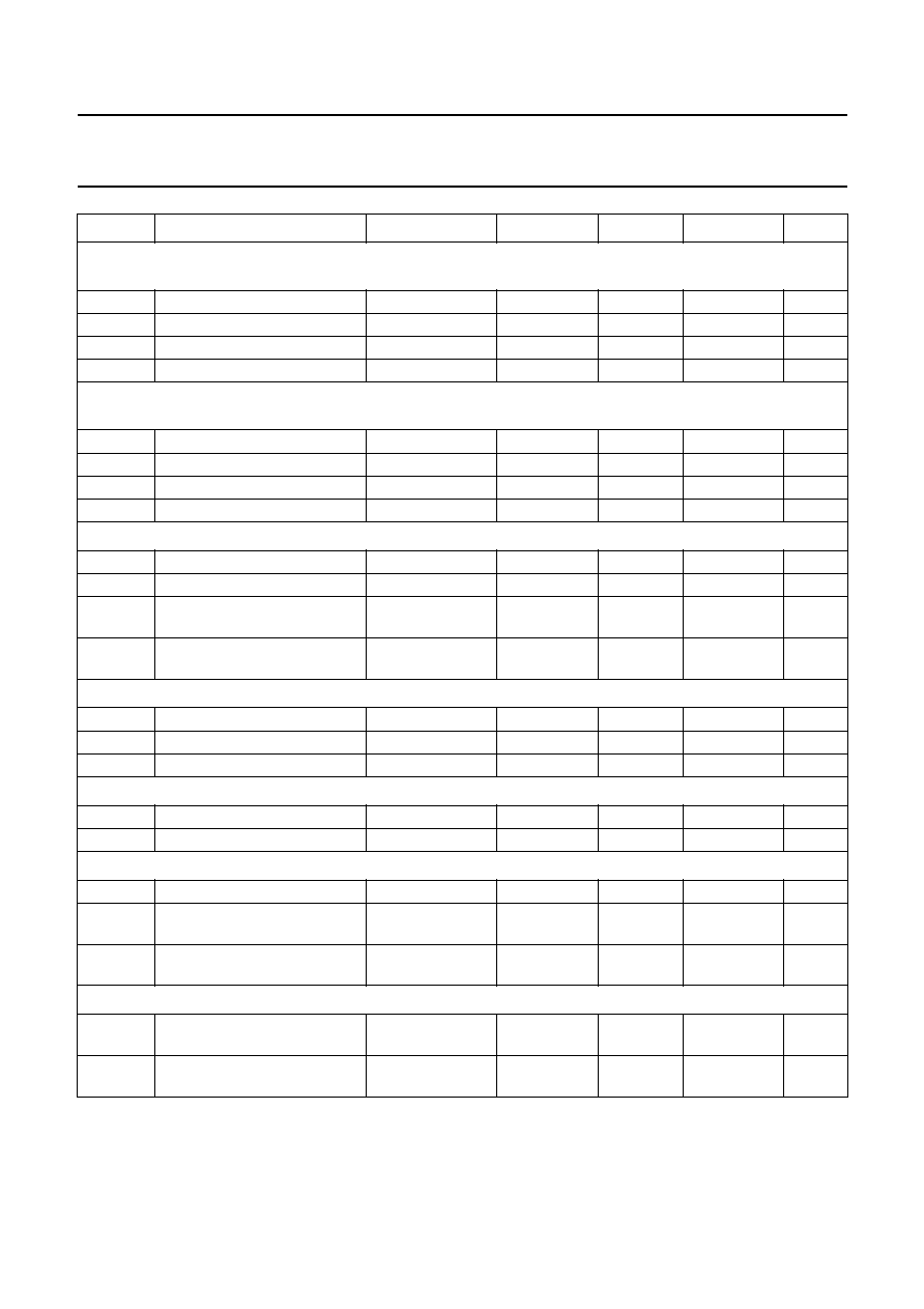
LIMITING VALUES
In accordance with the Absolute Maximum Rating System (IEC 134).
Notes
1. Equivalent to discharging a 100 pF capacitor through a 1.5 k
series resistor.
2. Equivalent to discharging a 200 pF capacitor through a 0
series resistor.
SYMBOL
PARAMETER
CONDITIONS
MIN.
MAX.
UNIT
V
DD
supply voltage
-
0.5
+6.5
V
V
I
input voltage
-
0.5
V
DD
+ 0.5
V
I
I
input current
-
20
mA
V
O
output voltage
-
0.5
+6.5
V
I
O
output current
-
20
mA
T
stg
storage temperature
-
65
+150
∞
C
T
amb
operating ambient temperature
-
40
+85
∞
C
V
es
electrostatic handling
Human Body Model (HBM)
note 1
-
2000
+2000
V
Machine Model (MM)
note 2
-
200
+200
V
May 1994
21
Philips Semiconductors
Preliminary specification
Adaptive allocation and scaling for PASC
coding in DCC systems
SAA2013
CHARACTERISTICS
V
DD
= 2.7 to 5.5 V; V
SS
= 0 V;T
amb
=
-
40 to 85
∞
C; unless otherwise specified; I
OL
and I
OH
derated by 75% for
V
DD
< 4.5 V.
SYMBOL
PARAMETER
CONDITIONS
MIN.
TYP.
MAX.
UNIT
Supply
V
DD
supply voltage
2.7
5.0
5.5
V
I
DD
supply current
V
DD
= 3.0 V
4
5
6
mA
V
DD
= 5.0 V
7
10
12
mA
I
stb
standby current
V
DD
= 5.0 V
-
-
400
µ
A
Inputs
V
IL
LOW level input voltage
0
-
0.3V
DD
V
V
IH
HIGH level input voltage
0.7V
DD
-
V
DD
V
I
LI
input leakage current
V
I
= 0 to V
DD
-
10
-
+10
µ
A
C
I
input capacitance
-
-
10
pF
Outputs
V
OL
LOW level output voltage
I
OL
= 4 mA
0
-
0.4
V
V
OH
HIGH level output voltage
I
OH
=
-
4 mA
V
DD
-
0.4
-
V
DD
V
C
L
load capacitance
-
-
30
pF
Inputs/outputs
V
IL
LOW level input voltage
0
-
0.3V
DD
V
V
IH
HIGH level input voltage
0.7V
DD
-
V
DD
V
I
LI
3-state leakage current
V
I
= 0 to V
DD
-
10
-
+10
µ
A
C
I
input capacitance
-
-
10
pF
V
OL
LOW level output voltage
I
OL
= 4 mA
0
-
0.4
V
V
OH
HIGH level output voltage
I
OH
=
-
4 mA
V
DD
-
0.4
-
V
DD
V
C
L
load capacitance
-
-
30
pF
Clock input CLK24
f
i
input frequency
see Fig.19
-
24.576
-
MHz
t
r
rise time
-
-
7
ns
t
f
fall time
-
-
7
ns
t
cH
HIGH time
10
-
-
ns
t
cL
LOW time
10
-
-
ns
Clock input FS256
f
i
input frequency
f
s
= 48 kHz
-
12.288
-
MHz
f
s
= 44.1 kHz
-
11.2896
-
MHz
f
s
= 32 kHz
-
8.192
-
MHz
t
r
rise time
-
-
7
ns
t
f
fall time
-
-
7
ns
t
cH
HIGH time
35
-
-
ns
t
cL
LOW time
35
-
-
ns
May 1994
22
Philips Semiconductors
Preliminary specification
Adaptive allocation and scaling for PASC
coding in DCC systems
SAA2013
Inputs FSYNC, FRESET, FDIR, FDWS, L3MODEM, L3CLKM, L3DATAM and L3DATAC;
referenced to CLK24 rising edge; see Fig.20; SLEEP = RESET = POR = logic 0
t
su
set-up time
15
-
-
ns
t
h
hold time
20
-
-
ns
t
r
rise time
-
-
200
ns
t
f
fall time
-
-
200
ns
Inputs FDAI, FDCL, FDWS, FRESET and FDIR; referenced to FS256 rising edge;
SLEEP = RESET = POR = logic 0
t
su
set-up time
15
-
-
ns
t
h
hold time
20
-
-
ns
t
r
rise time
-
-
200
ns
t
f
fall time
-
-
200
ns
Output FDAO; referenced to FS256 rising edge; see Fig.21; SLEEP = RESET = POR = logic 0
t
h
hold time
C
L
= 7.5 pF
0
-
-
ns
t
d
delay time
C
L
= 30 pF
-
-
30
ns
t
d3
output delay time after FDCL
HIGH
see Fig.22
2T
c256
-
10
(1)
-
-
ns
t
d4
output delay time after FDCL
HIGH
see Fig.22
-
-
3T
c256
+ 60
(1)
ns
Input FDCL; see Fig.22
T
c
FDCL period
280
4T
c256
(1)
-
ns
t
cH
FDCL HIGH time
T
c256
+ 35
(1)
-
-
ns
t
cL
FDCL LOW time
T
c256
+ 35
(1)
-
-
ns
Inputs FDAI and FDWS; see Fig.22
t
su1
set-up time before FDCL HIGH
3T
c256
+ 60
(1)
-
-
ns
t
h1
hold time after FDCL HIGH
T
c256
+ 20
(1)
-
-
ns
Input FRESET; see Fig.4
t
H
FRESET HIGH time
1280
-
-
ns
t
su
FDIR set-up time before
FRESET LOW
0
210
-
ns
t
h
FDIR hold time after FRESET
LOW
9T
c24
(2)
370
-
ns
SLEEP and RESET timing; see Fig.5; LOWPWR = logic 1
t
h
RESET hold time after SLEEP
LOW
5T
c24
(2)
210
-
ns
t
d
CLK24 disable after SLEEP
HIGH
9T
c24
(2)
370
-
ns
SYMBOL
PARAMETER
CONDITIONS
MIN.
TYP.
MAX.
UNIT

May 1994
23
Philips Semiconductors
Preliminary specification
Adaptive allocation and scaling for PASC
coding in DCC systems
SAA2013
L3 interface timing; microcontroller to SAA2013
A
DDRESS MODE
;
SEE
F
IG
.16
t
d1
L3MODEM LOW to L3CLKM
LOW
190
-
-
ns
t
cH
L3CLKM HIGH time
250
-
-
ns
t
cL
L3CLKM LOW time
250
-
-
ns
t
su1
L3DATAM input set-up time
before L3CLKM HIGH
190
-
-
ns
t
h1
L3DATAM input hold time
after L3CLKM HIGH
30
-
-
ns
t
h2
L3CLKM HIGH before
L3MODEM HIGH
190
-
-
ns
D
ATA MODE
;
SEE
F
IG
.17
t
d1
L3MODEM HIGH to L3CLKM
LOW delay time
190
-
-
ns
t
cH
L3CLKM HIGH time
250
-
-
ns
t
cL
L3CLKM LOW time
250
-
-
ns
t
su1
L3DATAM input set-up time
before L3CLKM HIGH
190
-
-
ns
t
h1
L3DATAM input hold time
after L3CLKM HIGH
30
-
-
ns
t
h2
L3CLKM HIGH before
L3MODEM LOW
190
-
-
ns
t
d3
L3MODEM HIGH to L3DATAM
output valid
-
-
380
ns
t
h3
L3DATAM output hold time
after L3CLKM HIGH
120
-
-
ns
t
d4
L3CLKM HIGH to L3DATAM
output valid delay time
-
-
360
ns
between bits 7
and 8; no halt
mode used
-
-
530
ns
t
d2
L3MODEM HIGH to L3DATAM
output enabled delay time
0
-
50
ns
t
d5
L3MODEM LOW to L3DATAM
output disabled delay time
0
-
50
ns
SYMBOL
PARAMETER
CONDITIONS
MIN.
TYP.
MAX.
UNIT

May 1994
24
Philips Semiconductors
Preliminary specification
Adaptive allocation and scaling for PASC
coding in DCC systems
SAA2013
H
ALT MODE
;
SEE
F
IG
.18
t
L
L3MODEM LOW time
190
-
-
ns
t
d1
L3MODEM HIGH to L3CLKM
HIGH delay time
190
-
-
ns
t
h2
L3CLKM HIGH before
L3MODEM LOW
190
-
-
ns
t
d2
L3MODEM HIGH to L3DATAM
output enabled delay time
0
-
50
ns
t
d5
L3MODEM LOW to L3DATAM
output disabled delay time
0
-
50
ns
L3 interface timing; SAA2013 to SAA2003
A
DDRESS MODE
;
SEE
F
IG
.14
t
d1
L3MODEC LOW to L3CLKC
LOW delay time
190
-
-
ns
t
cH
L3CLKC HIGH time
210
-
-
ns
t
cL
L3CLKC LOW time
210
-
-
ns
t
h2
L3CLKC HIGH time before
L3MODEC HIGH
190
-
-
ns
t
d3
L3MODEC LOW to L3DATAC
output valid delay time
-
-
380
ns
t
h1
L3DATAC output hold time
after L3CLKC HIGH
120
-
-
ns
t
d4
L3CLKC HIGH to L3DATAC
output valid delay time
-
-
360
ns
t
d2
L3MODEC LOW to L3DATAC
output enabled delay time
0
-
50
ns
t
d5
L3MODEC HIGH to L3DATAC
output disabled delay time
0
-
50
ns
SYMBOL
PARAMETER
CONDITIONS
MIN.
TYP.
MAX.
UNIT

May 1994
25
Philips Semiconductors
Preliminary specification
Adaptive allocation and scaling for PASC
coding in DCC systems
SAA2013
Notes
1. T
c256
is a clock period of FS256.
2. T
c24
is a clock period of CLK24.
D
ATA MODE
;
SEE
F
IG
.15
t
d1
L3MODEC HIGH to L3CLKC
LOW
190
-
-
ns
t
cH
L3CLKC HIGH time
210
-
-
ns
t
cL
L3CLKC LOW time
210
-
-
ns
t
su1
L3DATAC input set-up time
before L3CLKC HIGH
100
-
-
ns
t
h1
L3DATAC input hold time after
L3CLKC HIGH
30
-
-
ns
t
h2
L3CLKC HIGH time before
L3MODEC LOW
190
-
-
ns
t
d3
L3MODEC HIGH to L3DATAC
output valid
-
-
380
ns
t
h3
L3DATAC output hold time
after L3CLKC HIGH
120
-
-
ns
t
d4
L3CLKC HIGH to L3DATAC
output valid
-
-
360
ns
between bits 7
and 8; no halt
mode used
-
-
530
ns
H
ALT MODE
;
SEE
F
IG
.18
t
L
L3MODEC LOW time
190
-
-
ns
t
d1
L3MODEC HIGH to L3CLKC
HIGH delay time
190
-
-
ns
t
h2
L3CLKC HIGH time before
L3MODEC LOW
190
-
-
ns
L3 interface delays in bypassed mode; LOWPWR = logic 1
t
pd1
propagation delay from
L3MODEM to L3MODEC;
L3DATAM to L3DATAC;
L3CLKM to L3CLKC
-
-
35
ns
t
pd2
propagation delay from
L3DATAM to L3DATAC;
L3CLKM to L3CLKC
-
20
-
+4
ns
t
pd3
propagation delay from
L3DATAM to L3DATAC;
L3MODEM to L3MODEC
-
20
-
+4
ns
SYMBOL
PARAMETER
CONDITIONS
MIN.
TYP.
MAX.
UNIT

May 1994
26
Philips Semiconductors
Preliminary specification
Adaptive allocation and scaling for PASC
coding in DCC systems
SAA2013
PACKAGE OUTLINE
handbook, full pagewidth
X
A
B
10.1
9.9
12.9
12.3
0.15
M
B
0.40
0.20
pin 1 index
1
44
34
33
23
22
11
0.40
0.20
0.15 M A
0.8
12
0.8
10.1
9.9
12.9
12.3
S
0.1 S
seating
plane
1.2
0.8
(4x)
1.2
0.8
(4x)
0.95
0.55
MBB944 - 2
detail X
0.85
0.75
0.25
0.14
2.10
1.70
0 to 10
o
1.85
1.65
0.25
0.05
Fig.24 Plastic quad flat-pack, 44-pin (short) (QFP44SL).
Dimensions in mm.

May 1994
27
Philips Semiconductors
Preliminary specification
Adaptive allocation and scaling for PASC
coding in DCC systems
SAA2013
SOLDERING
Plastic quad flat-packs
B
Y WAVE
During placement and before soldering, the component
must be fixed with a droplet of adhesive. After curing the
adhesive, the component can be soldered. The adhesive
can be applied by screen printing, pin transfer or syringe
dispensing.
Maximum permissible solder temperature is 260
∞
C, and
maximum duration of package immersion in solder bath is
10 s, if allowed to cool to less than 150
∞
C within 6 s.
Typical dwell time is 4 s at 250
∞
C.
A modified wave soldering technique is recommended
using two solder waves (dual-wave), in which a turbulent
wave with high upward pressure is followed by a smooth
laminar wave. Using a mildly-activated flux eliminates the
need for removal of corrosive residues in most
applications.
B
Y SOLDER PASTE REFLOW
Reflow soldering requires the solder paste (a suspension
of fine solder particles, flux and binding agent) to be
applied to the substrate by screen printing, stencilling or
pressure-syringe dispensing before device placement.
Several techniques exist for reflowing; for example,
thermal conduction by heated belt, infrared, and
vapour-phase reflow. Dwell times vary between 50 and
300 s according to method. Typical reflow temperatures
range from 215 to 250
∞
C.
Preheating is necessary to dry the paste and evaporate
the binding agent. Preheating duration: 45 min at 45
∞
C.
R
EPAIRING SOLDERED JOINTS
(
BY HAND
-
HELD SOLDERING
IRON OR PULSE
-
HEATED SOLDER TOOL
)
Fix the component by first soldering two, diagonally
opposite, end pins. Apply the heating tool to the flat part of
the pin only. Contact time must be limited to 10 s at up to
300
∞
C. When using proper tools, all other pins can be
soldered in one operation within 2 to 5 s at between 270
and 320
∞
C. (Pulse-heated soldering is not recommended
for SO packages.)
For pulse-heated solder tool (resistance) soldering of VSO
packages, solder is applied to the substrate by dipping or
by an extra thick tin/lead plating before package
placement.

May 1994
28
Philips Semiconductors
Preliminary specification
Adaptive allocation and scaling for PASC
coding in DCC systems
SAA2013
DEFINITIONS
LIFE SUPPORT APPLICATIONS
These products are not designed for use in life support appliances, devices, or systems where malfunction of these
products can reasonably be expected to result in personal injury. Philips customers using or selling these products for
use in such applications do so at their own risk and agree to fully indemnify Philips for any damages resulting from such
improper use or sale.
Data sheet status
Objective specification
This data sheet contains target or goal specifications for product development.
Preliminary specification
This data sheet contains preliminary data; supplementary data may be published later.
Product specification
This data sheet contains final product specifications.
Limiting values
Limiting values given are in accordance with the Absolute Maximum Rating System (IEC 134). Stress above one or
more of the limiting values may cause permanent damage to the device. These are stress ratings only and operation
of the device at these or at any other conditions above those given in the Characteristics sections of the specification
is not implied. Exposure to limiting values for extended periods may affect device reliability.
Application information
Where application information is given, it is advisory and does not form part of the specification.
The Digital Compact Cassette logo is a registered trade mark of Philips Electronics N.V.

May 1994
29
Philips Semiconductors
Preliminary specification
Adaptive allocation and scaling for PASC
coding in DCC systems
SAA2013
NOTES

May 1994
30
Philips Semiconductors
Preliminary specification
Adaptive allocation and scaling for PASC
coding in DCC systems
SAA2013
NOTES

May 1994
31
Philips Semiconductors
Preliminary specification
Adaptive allocation and scaling for PASC
coding in DCC systems
SAA2013
NOTES

Philips Semiconductors
Philips Semiconductors ≠ a worldwide company
Argentina: IEROD, Av. Juramento 1992 - 14.b, (1428)
BUENOS AIRES, Tel. (541)786 7633, Fax. (541)786 9367
Australia: 34 Waterloo Road, NORTH RYDE, NSW 2113,
Tel. (02)805 4455, Fax. (02)805 4466
Austria: Triester Str. 64, A-1101 WIEN, P.O. Box 213,
Tel. (01)60 101-1236, Fax. (01)60 101-1211
Belgium: Postbus 90050, 5600 PB EINDHOVEN, The Netherlands,
Tel. (31)40 783 749, Fax. (31)40 788 399
Brazil: Rua do Rocio 220 - 5
th
floor, Suite 51,
CEP: 04552-903-S√O PAULO-SP, Brazil.
P.O. Box 7383 (01064-970).
Tel. (011)821-2327, Fax. (011)829-1849
Canada: INTEGRATED CIRCUITS:
Tel. (800)234-7381, Fax. (708)296-8556
DISCRETE SEMICONDUCTORS: 601 Milner Ave,
SCARBOROUGH, ONTARIO, M1B 1M8,
Tel. (0416)292 5161 ext. 2336, Fax. (0416)292 4477
Chile: Av. Santa Maria 0760, SANTIAGO,
Tel. (02)773 816, Fax. (02)777 6730
Colombia: IPRELENSO LTDA, Carrera 21 No. 56-17,
77621 BOGOTA, Tel. (571)249 7624/(571)217 4609,
Fax. (571)217 4549
Denmark: Prags Boulevard 80, PB 1919, DK-2300 COPENHAGEN S,
Tel. (032)88 2636, Fax. (031)57 1949
Finland: Sinikalliontie 3, FIN-02630 ESPOO,
Tel. (9)0-50261, Fax. (9)0-520971
France: 4 Rue du Port-aux-Vins, BP317,
92156 SURESNES Cedex,
Tel. (01)4099 6161, Fax. (01)4099 6427
Germany: PHILIPS COMPONENTS UB der Philips G.m.b.H.,
P.O. Box 10 63 23, 20043 HAMBURG,
Tel. (040)3296-0, Fax. (040)3296 213.
Greece: No. 15, 25th March Street, GR 17778 TAVROS,
Tel. (01)4894 339/4894 911, Fax. (01)4814 240
Hong Kong: PHILIPS HONG KONG Ltd., Components Div.,
6/F Philips Ind. Bldg., 24-28 Kung Yip St., KWAI CHUNG, N.T.,
Tel. (852)424 5121, Fax. (852)428 6729
India: Philips INDIA Ltd, Components Dept,
Shivsagar Estate, A Block ,
Dr. Annie Besant Rd. Worli, Bombay 400 018
Tel. (022)4938 541, Fax. (022)4938 722
Indonesia: Philips House, Jalan H.R. Rasuna Said Kav. 3-4,
P.O. Box 4252, JAKARTA 12950,
Tel. (021)5201 122, Fax. (021)5205 189
Ireland: Newstead, Clonskeagh, DUBLIN 14,
Tel. (01)640 000, Fax. (01)640 200
Italy: PHILIPS COMPONENTS S.r.l.,
Viale F. Testi, 327, 20162 MILANO,
Tel. (02)6752.3302, Fax. (02)6752 3300.
Japan: Philips Bldg 13-37, Kohnan 2 -chome, Minato-ku, TOKYO 108,
Tel. (03)3740 5028, Fax. (03)3740 0580
Korea: (Republic of) Philips House, 260-199 Itaewon-dong,
Yongsan-ku, SEOUL, Tel. (02)794-5011, Fax. (02)798-8022
Malaysia: No. 76 Jalan Universiti, 46200 PETALING JAYA,
SELANGOR, Tel. (03)750 5214, Fax. (03)757 4880
Mexico: Philips Components, 5900 Gateway East, Suite 200,
EL PASO, TX 79905, Tel. 9-5(800)234-7381, Fax. (708)296-8556
Netherlands: Postbus 90050, 5600 PB EINDHOVEN, Bldg. VB
Tel. (040)783749, Fax. (040)788399
New Zealand: 2 Wagener Place, C.P.O. Box 1041, AUCKLAND,
Tel. (09)849-4160, Fax. (09)849-7811
Norway: Box 1, Manglerud 0612, OSLO,
Tel. (022)74 8000, Fax. (022)74 8341
Pakistan: Philips Electrical Industries of Pakistan Ltd.,
Exchange Bldg. ST-2/A, Block 9, KDA Scheme 5, Clifton,
KARACHI 75600, Tel. (021)587 4641-49,
Fax. (021)577035/5874546.
Philippines: PHILIPS SEMICONDUCTORS PHILIPPINES Inc,
106 Valero St. Salcedo Village, P.O. Box 2108 MCC, MAKATI,
Metro MANILA, Tel. (02)810 0161, Fax. (02)817 3474
Portugal: PHILIPS PORTUGUESA, S.A.,
Rua dr. AntÛnio Loureiro Borges 5, Arquiparque - Miraflores,
Apartado 300, 2795 LINDA-A-VELHA,
Tel. (01)14163160/4163333, Fax. (01)14163174/4163366.
Singapore: Lorong 1, Toa Payoh, SINGAPORE 1231,
Tel. (65)350 2000, Fax. (65)251 6500
South Africa: S.A. PHILIPS Pty Ltd., Components Division,
195-215 Main Road Martindale, 2092 JOHANNESBURG,
P.O. Box 7430 Johannesburg 2000,
Tel. (011)470-5911, Fax. (011)470-5494.
Spain: Balmes 22, 08007 BARCELONA,
Tel. (03)301 6312, Fax. (03)301 42 43
Sweden: Kottbygatan 7, Akalla. S-164 85 STOCKHOLM,
Tel. (0)8-632 2000, Fax. (0)8-632 2745
Switzerland: Allmendstrasse 140, CH-8027 ZÐRICH,
Tel. (01)488 2211, Fax. (01)481 77 30
Taiwan: PHILIPS TAIWAN Ltd., 23-30F, 66, Chung Hsiao West
Road, Sec. 1. Taipeh, Taiwan ROC, P.O. Box 22978,
TAIPEI 100, Tel. (02)388 7666, Fax. (02)382 4382.
Thailand: PHILIPS ELECTRONICS (THAILAND) Ltd.,
209/2 Sanpavuth-Bangna Road Prakanong,
Bangkok 10260, THAILAND,
Tel. (662)398-0141, Fax. (662)398-3319.
Turkey: Talatpasa Cad. No. 5, 80640 GÐLTEPE/ISTANBUL,
Tel. (0 212)279 2770, Fax. (0212)269 3094
United Kingdom: Philips Semiconductors Limited, P.O. Box 65,
Philips House, Torrington Place, LONDON, WC1E 7HD,
Tel. (071)436 41 44, Fax. (071)323 03 42
United States: INTEGRATED CIRCUITS:
811 East Arques Avenue, SUNNYVALE, CA 94088-3409,
Tel. (800)234-7381, Fax. (708)296-8556
DISCRETE SEMICONDUCTORS: 2001 West Blue Heron Blvd.,
P.O. Box 10330, RIVIERA BEACH, FLORIDA 33404,
Tel. (800)447-3762 and (407)881-3200, Fax. (407)881-3300
Uruguay: Coronel Mora 433, MONTEVIDEO,
Tel. (02)70-4044, Fax. (02)92 0601
For all other countries apply to: Philips Semiconductors,
International Marketing and Sales, Building BAF-1,
P.O. Box 218, 5600 MD, EINDHOVEN, The Netherlands,
Telex 35000 phtcnl, Fax. +31-40-724825
SCD31
© Philips Electronics N.V. 1994
All rights are reserved. Reproduction in whole or in part is prohibited without the
prior written consent of the copyright owner.
The information presented in this document does not form part of any quotation
or contract, is believed to be accurate and reliable and may be changed without
notice. No liability will be accepted by the publisher for any consequence of its
use. Publication thereof does not convey nor imply any license under patent- or
other industrial or intellectual property rights.
Printed in The Netherlands
513061/1500/01/pp32
Date of release: May 1994
Document order number:
9397 731 90011