 | –≠–ª–µ–∫—Ç—Ä–æ–Ω–Ω—ã–π –∫–æ–º–ø–æ–Ω–µ–Ω—Ç: SAA2502 | –°–∫–∞—á–∞—Ç—å:  PDF PDF  ZIP ZIP |

DATA SHEET
Preliminary specification
Supersedes data of 1997 Apr 18
File under Integrated Circuits, IC01
1997 Nov 17
INTEGRATED CIRCUITS
SAA2502
ISO/MPEG Audio Source Decoder

1997 Nov 17
2
Philips Semiconductors
Preliminary specification
ISO/MPEG Audio Source Decoder
SAA2502
CONTENTS
1
FEATURES
2
APPLICATIONS
3
GENERAL DESCRIPTION
4
ORDERING INFORMATION
5
BLOCK DIAGRAM
6
PINNING
7
FUNCTIONAL DESCRIPTION
7.1
Basic functionality
7.2
Clock generator module
7.2.1
External sample clock
7.2.2
Free running internal sample clock
7.2.3
Locked internal sample clock
7.2.4
Limited sampling frequency support for internal
sampling clocks
7.3
Input interface module
7.3.1
Master input mode
7.3.2
Slave input mode
7.3.3
Buffer controlled input mode
7.4
Decoder core
7.4.1
Frame synchronization to input data streams
7.4.2
Master input mode bit rate generation
7.4.3
Sample clock generation
7.4.4
Decoder precision
7.4.5
Scale factor CRC protection
7.4.6
Handling of errors in the coded input data
7.4.7
Dynamic range compression
7.4.8
Baseband audio processing
7.4.9
Decoder latency time
7.5
Output interface module
7.5.1
I
2
S output
7.5.2
SPIDF output
7.5.3
Bit serial analog output
7.6
Control interface module
7.6.1
Resetting
7.6.2
Interrupts
7.6.3
Microcontroller interface
7.6.4
Initialization
7.6.5
Transfer protocols
7.6.6
Local registers
8
APPENDIX
8.1
L3 interface specification
8.1.1
Introduction
8.1.2
Example of a data transfer
8.1.3
Timing requirements
8.1.4
Timing
9
LIMITING VALUES
10
DC CHARACTERISTICS
11
AC CHARACTERISTICS
11.1
Host interface: CDATA, CCLK and CMODE
12
APPLICATION INFORMATION
13
PACKAGE OUTLINE
14
SOLDERING
14.1
Introduction
14.2
Reflow soldering
14.3
Wave soldering
14.4
Repairing soldered joints
15
DEFINITIONS
16
LIFE SUPPORT APPLICATIONS

1997 Nov 17
3
Philips Semiconductors
Preliminary specification
ISO/MPEG Audio Source Decoder
SAA2502
1
FEATURES
∑
Low sampling frequency decoding possibilities (24 kHz,
22.05 kHz and 16 kHz) of MPEG2 are supported
∑
A variety of output formats are supported: I
2
S, SPDIF
and 256 or more times oversampled bit serial analog
stereo
∑
Automatic internal dynamic range compression
algorithm using programmable compression
parameters
∑
Non byte-aligned coded input data is handled
∑
Built-in provisions to generate high quality sampling
clocks for all six supported sampling frequencies; these
sampling clocks may locked to an external PLL to
support an extensive list of input data reference clock
frequencies
∑
Bit-rate and sampling-rate settings may be overruled by
the microcontroller while the SAA2502 is trying to
establish frame synchronization
∑
Input interface mode which requests data based on
input buffer content, enables the handling of variable
bit-rate input streams and input data offered in (fixed
length) bursts
∑
An interrupt output pin which can generate interrupt
requests at the occurrence of various events;
consequently polling by the microcontroller is not
needed in most situations
∑
L3 and the I
2
C-bus microcontroller interface protocols
are supported
∑
The control interface is always fully operational (also
while STOP is asserted)
∑
CRC protection of scale factors is provided for all
supported sample frequencies.
2
APPLICATIONS
∑
Astra Digital Radio (ADR)
∑
Digital Audio Broadcast (DAB)
∑
Digital Versatile Disc (DVD)
∑
Digital Video Broadcast (DVB)
∑
General purpose MPEG2 audio decoding.
3
GENERAL DESCRIPTION
The SAA2502 is a second generation ISO/MPEG audio
source decoder. The device specification has been
enhanced with respect to the SAA2500 and SAA2501 ICs
and therefore it offers in principle all features of its
predecessors.
It supports layer I and II of MPEG1 and the MPEG2
requirements for a stereo decoder.
4
ORDERING INFORMATION
TYPE NUMBER
PACKAGE
NAME
DESCRIPTION
VERSION
SAA2502H
QFP44
plastic quad flat package; 44 leads (lead length 1.3 mm);
body 10
◊
10
◊
1.75 mm
SOT307-2
1997 Nov 17
4
Philips Semiconductors
Preliminary specification
ISO/MPEG Audio Source Decoder
SAA2502
5
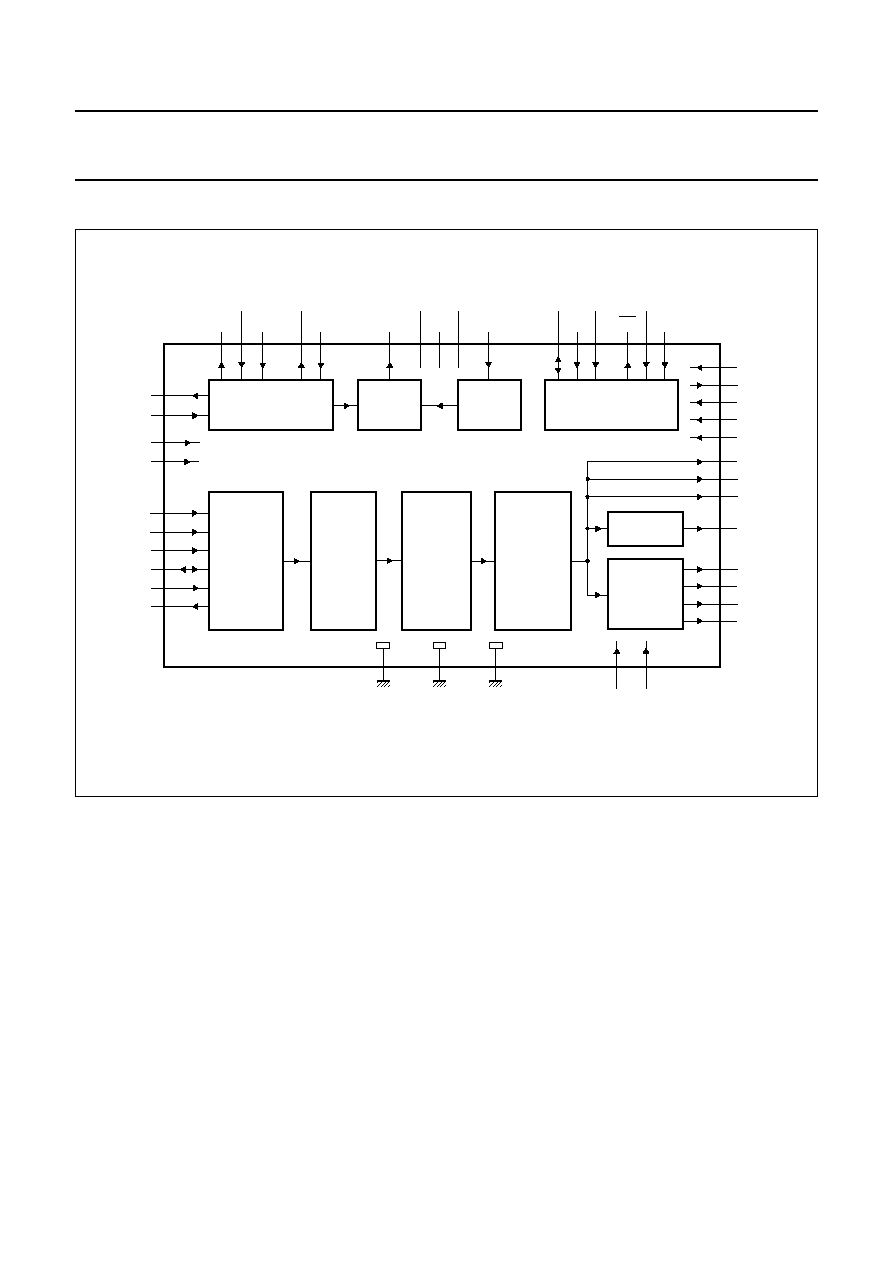
BLOCK DIAGRAM
Fig.1 Block diagram.
handbook, full pagewidth
MGE469
INPUT
INTERFACE
DEMULTI-
PLEXER
DEQUANTI-
ZATION
AND
SCALING
SYNTHESIS
SUB-BAND
FILTER
DIGITAL-TO-
ANALOG
CONVERTER
SPDIF
ENCODER
CLOCK GENERATOR
PHASE
COMPA-
RATOR
DIVIDER
DECODING
CONTROL
1
25
40
43
15
17
19
14
20
13
16
28
42
37
36
35
34
38
39
6
4
2
3
5
21
24
41
33
11
12
10
9
7
8
22
23
26
27
29
32
31
18 30 44
SAA2502
MCLKOUT
MCLKIN
MCLK24
X22OUT
X22IN
PHDIF
VDD1
VDD2
VDD3
REFCLK
CDATA
CCLK
CMODE
INT
STOP
RESET
TDI
TDO
TCK
TMS
TRST
SD
SCK
WS
SPDIF
LFTPOS
LFTNEG
RGTPOS
RGTNEG
REFN
REFP
GND1
GND2
GND3
CDRQ
CDVAL
CDCL
CDSY
CDEF
CD
TC1
TC0
FSCLKIN
FSCLK

1997 Nov 17
5
Philips Semiconductors
Preliminary specification
ISO/MPEG Audio Source Decoder
SAA2502
6
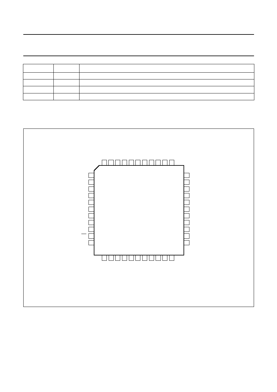
PINNING
SYMBOL
PIN
DESCRIPTION
FSCLK
1
sample rate clock output; buffered signal
SCK
2
baseband audio data I
2
S clock output
SD
3
baseband audio I
2
S data output
WS
4
baseband audio data I
2
S word select output
TRST
5
boundary scan test reset input
SPDIF
6
SPDIF baseband audio output
CCLK
7
L3 clock/I
2
C-bus bit clock input
CDATA
8
L3 data/I
2
C-bus serial data input/output; note 1
CMODE
9
L3 mode (address/data select input)
INT
10
interrupt request output; active LOW; note 1
RESET
11
master reset input
STOP
12
soft reset/stop decoding input
CDRQ
13
coded data request output
CDCL
14
coded data bit clock input/output; note 2
CD
15
MPEG coded data input
GND1
16
ground 1
CDEF
17
coded data error flag input
V
DD1
18
supply voltage 1
CDSY
19
coded data byte or frame sync input
CDVAL
20
coded data valid flag input
TMS
21
boundary scan test mode select input
REFCLK
22
PLL reference clock input
PHDIF
23
PLL phase comparator output; note 2
TCK
24
boundary scan test clock input
FSCLKIN
25
sample rate clock input
X22IN
26
22.579 MHz clock oscillator input or signal input
X22OUT
27
22.579 MHz clock oscillator output
GND2
28
ground 2
MCLK24
29
master clock frequency indication input
V
DD2
30
supply voltage 2
MCLKOUT
31
master clock oscillator output
MCLKIN
32
master clock oscillator input or signal input
TDI
33
boundary scan test data input
RGTPOS
34
analog right channel positive output
RGTNEG
35
analog right channel negative output
REFN
36
low reference voltage input for analog outputs
REFP
37
high reference voltage input for analog outputs
LFTNEG
38
analog left channel negative output
LFTPOS
39
analog left channel positive output
TC0
40
factory test scan chain control 0 input
1997 Nov 17
6
Philips Semiconductors
Preliminary specification
ISO/MPEG Audio Source Decoder
SAA2502
Notes
1. Output type is: open-drain.
2. Output type is: 3-state.
TDO
41
boundary scan test data output
GND3
42
ground 3
TC1
43
factory test scan chain control 1 input
V
DD3
44
supply voltage 3
SYMBOL
PIN
DESCRIPTION
Fig.2 Pin configuration.
1
2
3
4
5
6
7
8
9
10
11
33
32
31
30
29
28
27
26
25
24
23
12
13
14
15
16
17
18
19
20
21
22
44
43
42
41
40
39
38
37
36
35
34
SAA2502
MGE468
TDI
MCLKIN
MCLKOUT
VDD2
GND2
X22OUT
X22IN
FSCLKIN
TCK
PHDIF
FSCLK
SCK
SD
WS
TRST
SPDIF
CDATA
CMODE
RESET
MCLK24
TC1
GND3
TDO
TC0
LFTPOS
LFTNEG
REFN
RGTNEG
RGTPOS
V
DD3
REFP
CDRQ
CDCL
CD
GND1
CDEF
V
DD1
CDVAL
TMS
REFCLK
STOP
CDSY
CCLK
INT
1997 Nov 17
7
Philips Semiconductors
Preliminary specification
ISO/MPEG Audio Source Decoder
SAA2502
7
FUNCTIONAL DESCRIPTION
7.1
Basic functionality
From a functional point of view, several blocks can be
distinguished in the SAA2502. A clock generator section
derives the internally and externally required clock signals
from its clock inputs. The input interface section receives
or requests coded input data in one of the supported input
interface modes. The demultiplexer processor handles
frame synchronization, parsing, demultiplexing and error
concealment of the input data stream The de-quantization
and scaling processor performs the transformation and
scaling operations on the (demultiplexed) coded sample
representations in the input bitstream to yield sub-band
domain samples.
The sub-band samples are transferred to the synthesis
sub-band filter bank processor which reconstructs the
baseband audio samples. The output interface block
transforms the audio samples to the output formats
required by the different output ports.
The decoding control block houses the I
2
C-bus/L3
microcontroller interface, and handles the response to
external control signals. This section enables the
application to configure the SAA2502, to read its decoding
status, to read ancillary data and so on.
Several pins are reserved for boundary scan test (5 pins)
and factory test scan chain control (2 pins).
7.2
Clock generator module
The SAA2502 clock interfacing is designed for application
versatility. It consists of 9 signals (see Table 1).
The clock generator provides the following clock signals:
∑
Internal sample clocks
∑
External buffered sample clock FSCLK
∑
Processor master clock
∑
Coded input data bit clock
∑
Coded input data request clock
The module can be configured to operate in 3 different
modes of operation:
∑
External sample clock mode
∑
Free running internal sample clock mode
∑
Locked internal sample clock mode.
Clock generator operation mode must be stationary while
the device is in normal operation. Changing mode should
always be followed by a (soft) reset.
f
input bit rate
32
-----------------------------------
=
Table 1
Clock interfacing signals
SIGNAL
DIRECTION
FUNCTION
MCLKIN
input
master clock oscillator input or signal input
MCLKOUT
output
master clock oscillator output
MCLK24
input
master clock frequency indication
X22IN
input
22.5792 MHz clock oscillator input or signal input
X22OUT
output
22.5792 MHz clock oscillator output
FSCLKIN
input
external sample rate clock signal input
FSCLK
output
sample rate clock signal output
REFCLK
input
coded input data rate reference clock
PHDIF
output
phase difference indication output between reference clock and sample clock
1997 Nov 17
8
Philips Semiconductors
Preliminary specification
ISO/MPEG Audio Source Decoder
SAA2502
7.2.1
E
XTERNAL SAMPLE CLOCK
In applications where a 256
◊
f
s
sample clock is available,
the use of external crystals may be avoided by putting the
SAA2502 clock generator module in `external sample
clock mode'. Such mode setting may be realized by setting
control flag FSCINP of the control interface. In this event
the sample clock has to be provided to the FSCLKIN clock
input. If sample rate switching should be supported,
required clock frequency changes are the responsibility of
the application. After such a clock frequency change,
enforcement of a soft reset is advised.
In external sample clock mode (and only in that mode) the
clock generator module is able to accept a 384
◊
f
s
sample
clock input. If that mode of operation is desired the control
flag FSC384 should be set.
The FSCLK output is normally disabled in this mode.
If enabled (by setting control flag FSCENA) FSCLK will
produce a buffered copy of FSCLKIN.
X22IN, X22OUT, REFCLK and PHDIF are not used in this
mode. X22IN and REFCLK should be connected to GND
or V
DD
.
MCLKIN is used to provide the (free running) master clock.
This may either be achieved by applying a correct clock
signal to MCLKIN or by connecting a crystal between
MCLKIN and MCLKOUT. In external sample clock mode
(and only in that mode) the master clock may deviate from
24.576 MHz. The master clock frequency value required
depends on the state of pin MCLK24 (see Table 2).
Table 2
Master clock frequency setting by MCLK24
7.2.2
F
REE RUNNING INTERNAL SAMPLE CLOCK
This is the default mode of operation: 256
◊
f
s
for all six
supported sample rates is generated internally from the
clock frequencies supplied to MCLKIN (24.576 MHz) and
X22IN (22.5792 MHz) as shown in Table 3.
MCLK24
FREQUENCY
MINIMUM
MAXIMUM
GND
256
◊
f
s
12.288 MHz
(256
◊
48 kHz)
V
DD
512
◊
f
s
24.576 MHz
(512
◊
48 kHz)
Table 3
Internal sample clock (default mode)
Note
1. Asymmetrical FSCLK.
The main advantage of this mode is that the SAA2502
determines automatically which sampling rate is active
from the sampling rate setting of the input data bit stream,
and then selects either MCLKIN or X22IN divided by the
correct number as the sample clock source.
Therefore this mode is particularly suited in applications
supporting dynamically varying sampling rates.
The required clocks may either be applied to MCLKIN
(respectively to X22IN) or be generated by connecting a
crystal between MCLKIN and MCLKOUT (respectively
between X22IN and X22OUT).
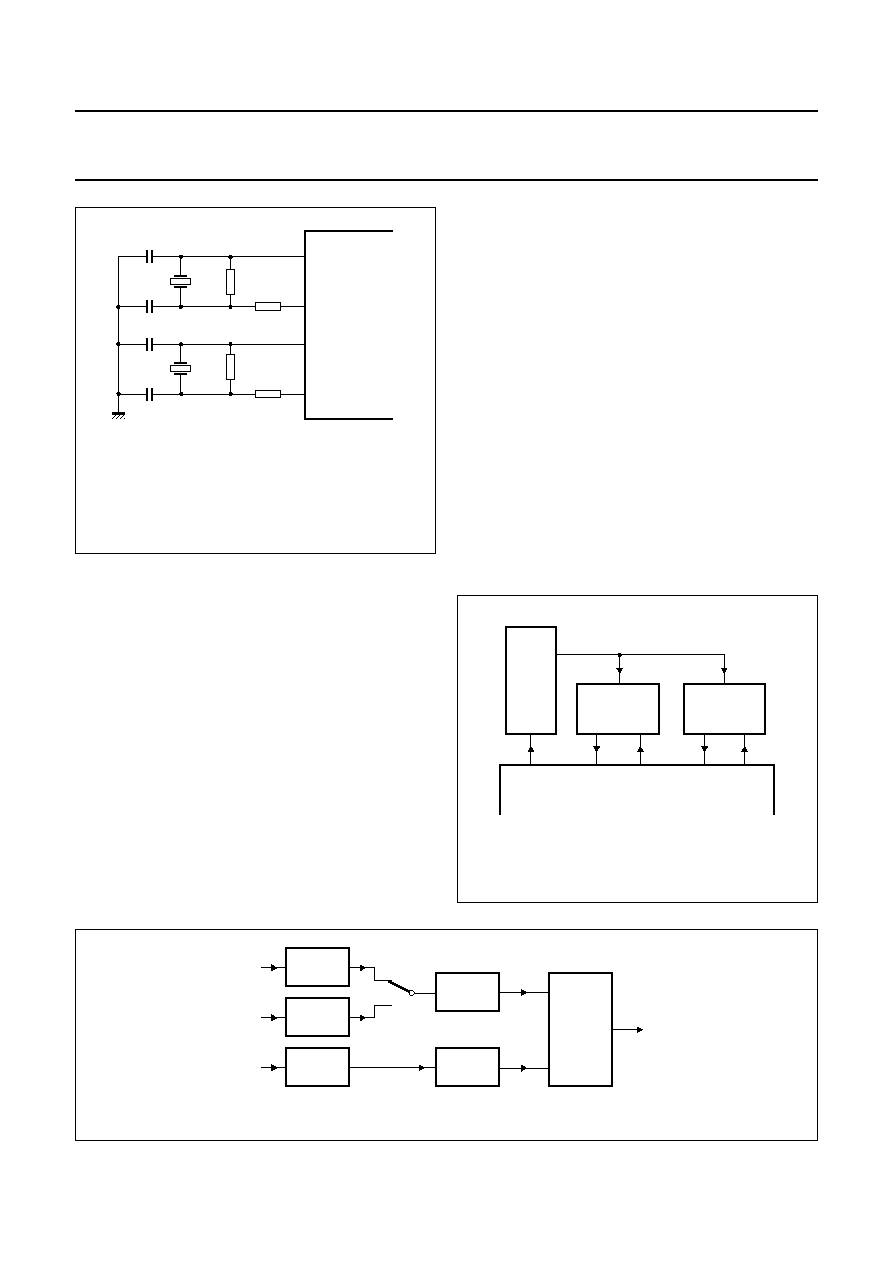
The recommended crystal oscillator configuration is
shown in Fig.3. The specified component values only
apply to crystals with a low equivalent series resistance
of <40
.
FSCLKIN, REFCLK and PHDIF are not used in this mode
(FSCLKIN and REFCLK should be connected to V
SS
or
V
DD
). MCLK24 has to be connected to V
DD
, while the
control flags FSCINP and FSC384 should be left in their
default (cleared) states. If the FSCLK output is enabled (by
setting control flag FSCENA) FSCLK will produce a
buffered version of 256
◊
f
s
.
SAMPLE
FREQUENCY
RESULTANT FREQUENCIES
(MHz)
256
◊
48 kHz
12.288
256
◊
44.1 kHz
11.2896
256
◊
32 kHz
8.192
(1)
256
◊
24 kHz
6.144
256
◊
22.05 kHz
5.6448
256
◊
16 kHz
4.096
24.576
2
------------------
22.5792
2
---------------------
24.576
3
------------------
24.576
4
------------------
22.5792
4
---------------------
24.576
6
------------------
1997 Nov 17
9
Philips Semiconductors
Preliminary specification
ISO/MPEG Audio Source Decoder
SAA2502
7.2.3
L
OCKED INTERNAL SAMPLE CLOCK
This mode differs from the previous one in just a single
aspect: the REFCLK and PHDIF pins are used to realize a
Phase-Locked Loop (PLL) which locks the 256
◊
f
s
sample
clock to the REFCLK reference clock. Because the real
goal is locking sample clock and bit rate, a reference clock
should be used which has a fixed relation to the input bit
rate. An example of such a PLL realization is shown in
Fig.4.
The phase comparator output PHDIF generates a signal
with a DC component proportional to the phase difference
between the internal signals SIG and REF (see Fig.5).
The 22.5792 MHz signal X22IN is divided by 147 and the
24.576 MHz signal MCLKIN is divided by 160. This results
in the same frequency (153.6 kHz) in both events.
One of the two signals is selected as input for the
programmable divide by N
1
unit. The selector is controlled
handbook, halfpage
MGE470
C2
C1
C3
C4
X1
X2
R1
R4
R2
R3
26
27
32
31
SAA2502
Fig.3 Crystal oscillator components.
C1 = C2 = C3 = C4 = 10 pF;
R1 = R4 = 100 k
;
R2 = R3 = 1 k
;
X1 = 22.5792 MHz;
X2 = 24.5760 MHz.
in such a way that SIG and 256
◊
f
s
will stem from the
same source. The divisor N
1
is programmable with
(1 to 16)
◊
8 as possible values.
REF on the other hand is derived from the REFCLK input.
Two programmable dividers in series are used here. N
2
may adopt one of 4 possible values: 5, 25, 125 or 625
while N
3
can be programmed to be 1 to 32. Because both
inputs of the phase comparator have to operate at identical
frequencies the next equation has to be obeyed:
or, written differently:
For a list of supported REFCLK frequency values
see Chapter 8.
The mode of operation of the phase comparator in Fig.5 is
programmable via the control flag PHSMOD:
REFCLK
N
2
N
3
◊
--------------------------
156.6 kHz
N
1
---------------------------
=
REFCLK
153.6 kHz
N
2
◊
N
3
◊
N
1
------------------------------------------------------
=
Fig.4 External PLL components.
handbook, halfpage
MGE471
LOW-
PASS
FILTER
24.576 MHz
VCXO
22.5792 MHZ
VCXO
PHDIF
MCLKIN
MCLKOUT
X22IN X22OUT
SAA2502
Fig.5 SAA2502 phase comparator.
handbook, full pagewidth
MGE472
DIVIDE BY
147
DIVIDE BY
160
DIVIDE BY
N2
DIVIDE BY
N3
DIVIDE BY
N1
PHASE
COMPA-
RATOR
X22IN
MCLKIN
REFCLK
153.6 kHz
SIG
REF
PHDIF
1997 Nov 17
10
Philips Semiconductors
Preliminary specification
ISO/MPEG Audio Source Decoder
SAA2502
7.2.3.1
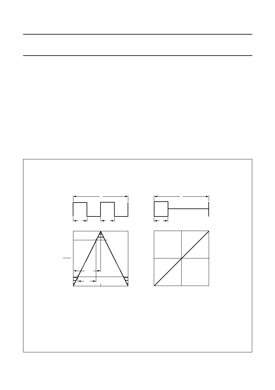
XOR mode
PHDIF is the XOR function of SIG and REF. The frequency
is twice the frequency of SIG and REF. The PHDIF output
carries a signal, switching between GND and V
DD
, with an
average value V
avg
which is a function of the phase
difference between SIG and REF (see left part of Fig.6).
The locking range in this mode of operation is maximum
for even values of N
3
(180 degrees phase difference) but
less for odd values of N
3
. It is minimum for N
3
= 3
(120 degrees phase difference).
7.2.3.2
Edge triggered mode
PHDIF is only influenced by the rising edges of SIG and
REF. Consequently its frequency is equal to the SIG and
REF frequency.
The electrical behaviour of the PHDIF output pin in this
mode is special:
PHDIF is HIGH from the rising edge of REF to the rising
edge of SIG and 3-stated elsewhere if REF is leading and
PHDIF is low from rising edge of SIG to rising edge of REF
and 3-stated elsewhere if REF is trailing. Therefore PHDIF
is NOT 3-stated during a portion t
up
of each cycle when it
acts as a pull-up device or during a portion t
down
of each
cycle when it acts as a pull-down device (see right part of
Fig.6).
As a result the locking range is always 360 degrees phase
difference. The output behaviour as function of phase
difference is non-symmetrical with reference to the vertical
axis, but a reversed mode is also available (by setting the
control flag PHSRVS).
Fig.6 PHDIF output behaviour.
handbook, full pagewidth
MGE473
REF to SIG phase difference
REF to SIG phase difference
max
min
0
o
180
o
360
o
-
180
o
0
o
+
180
o
0
1
5/6
1/6
Vavg
VDD
100%
100%
0%
tup
tdown
T
t1
t2
T
t
PHDIF
3-stated
XOR mode
edge triggered mode

1997 Nov 17
11
Philips Semiconductors
Preliminary specification
ISO/MPEG Audio Source Decoder
SAA2502
7.2.4
L
IMITED SAMPLING FREQUENCY SUPPORT FOR
INTERNAL SAMPLING CLOCKS
7.2.4.1
When sampling frequency is limited to
44.1 and/or 22.05 kHz:
In this event MCLKIN is only required to generate the
master clock frequency. Consequently the remarks on
MCLKIN frequency also apply in this special case.
7.2.4.2
When sampling frequency is limited to
48, 32, 24 and/or 16 kHz:
In this event X22IN is not required. Therefore X22IN
should be connected to V
SS
or V
DD
, but it is more efficient
to apply any available clock signal to X22IN. Because
44.1 kHz is the default initial sampling frequency it may
also be advisable to over-rule the sampling frequency after
a hard reset.
7.3
Input interface module
The input interface module handles the reception of the
coded input data stream.
The module can be configured to operate in 3 distinct
modes of operation:
∑
The master input mode
∑
The slave input mode
∑
The buffer controlled input mode.
Input interface mode must be stationary while the device is
in normal operation. Changing mode will result in an
(automatically generated) internal soft reset.
The inputs CD, CDVAL, CDEF and CDSY are all clocked
at the rising edge of the CDCL bit clock.
CDRQ changes at the falling edge of CDCL.
CDVAL = logic 0 indicates that CD and CDEF should be
ignored while CDVAL = logic 1 indicates that CD is a valid
coded input stream data bit (CDEF is then its error
attribute).
CDEF = logic 0 means that the value of CD may be
assumed to be reliable while CDEF = logic 1 means that
the value of CD is flagged as insecure (e.g. due to erratic
non-correctable channel behaviour). The value of CDEF
may be different for each data bit, but is combined by the
SAA2502 for every group of 8 (byte aligned) valid coded
input bits.
CDSY will only have effect when the SYMOD control flags
are set to 10 or 11. When SYMOD = 10 the valid input bit
at a rising edge of CDSY marks the start of a new byte
(when SYMOD = 11 it marks the start of a new MPEG
audio frame). Note that just the rising edge of CDSY is
important, the falling edge has no meaning.
If CDSY is used with SYMOD = 10 leading edges must be
frequent enough to assure fast byte alignment, if used with
SYMOD = 11 a leading edge must be present every frame.
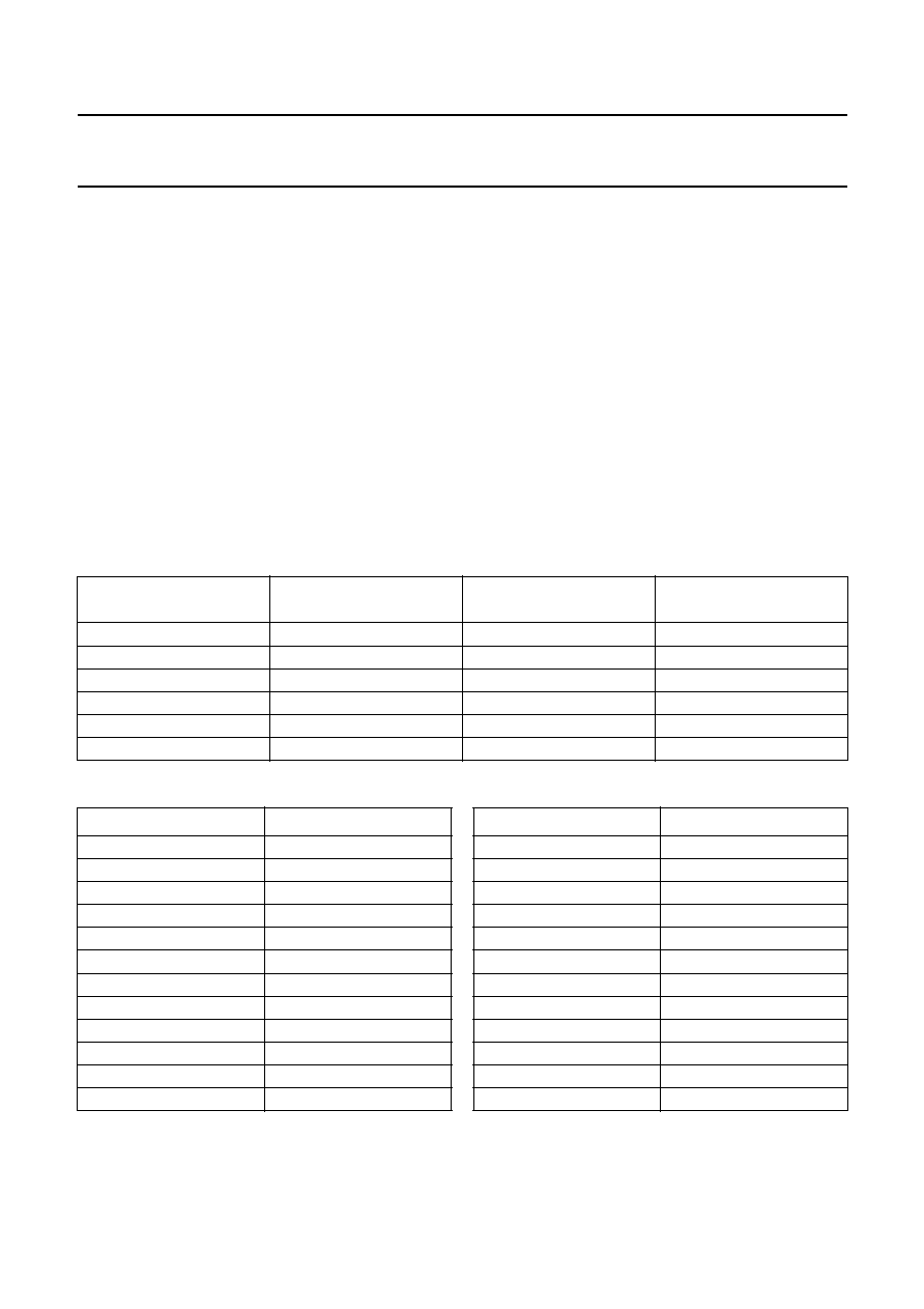
Leading edges of CDSY may occur while CDVAL is
(implicitly) high. Alternatively, a situation as shown in Fig.8
is also allowed, where CDSY has a rising edge while
CDVAL is low, i.e. during invalid data. The first valid CD bit
after the rising edge of CDVAL is then interpreted as the
first byte or frame bit.
The output pin CDRQ is used to request new coded input
data.
Table 4
Signals of coded data input interface
SIGNAL
DIRECTION
FUNCTION
CD
input
coded data input bit
CDVAL
input
coded data bit valid flag
CDEF
input
coded data bit error flag
CDSY
input
coded data sync (start of byte/frame) indication
CDCL
input/output
coded data bit clock
CDRQ
output
coded data request
1997 Nov 17
12
Philips Semiconductors
Preliminary specification
ISO/MPEG Audio Source Decoder
SAA2502
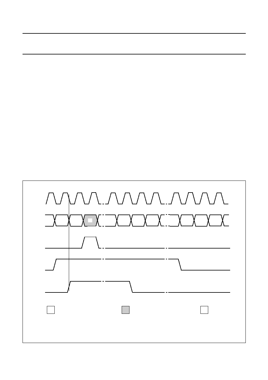
7.3.1
M
ASTER INPUT MODE
Master input mode is the default mode of operation. This
mode may also be enforced by setting the INMOD control
flags to 00. Which means that the SAA2502 will generate
requests for input data at regular intervals. CDVAL is not
used in this mode (it should be connected to V
SS
or V
DD
).
CDVAL is implicitly assumed to be logic 1 during the 2nd
up to (and including) the 17th bit slot after a rising or a
falling edge of CDRQ (see Fig.7). Thus signal CD should
carry the coded data in bursts of 16 valid bits.
In this mode the CDRQ frequency is locked to (i.e. derived
from) the 256
◊
f
s
clock. Its average value equals the bit
rate divided by 32.
The bit clock CDCL is output, its frequency is fixed:
when MCLK24 = logic 1
when MCLK24 = logic 0.
MCLK
32
------------------
MCLK
16
------------------
MPEG free format bit rate is NOT allowed in this mode.
Assume N is the number of CDCL periods between two
transitions of CDRQ, and R is the number of CDCL periods
to obtain the effective bit rate E (in kbits/s) at a CDCL
frequency of 768 kHz, i.e.
.
The SAA2502 keeps the average value of N exactly at R,
but individual values of N may vary between
N = round (R)
-
2 and N = round (R) +2.
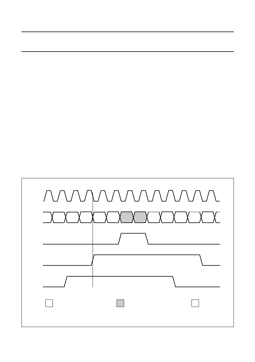
7.3.2
S
LAVE INPUT MODE
Slave input mode is activated by setting the INMOD control
flags to 0 1. Which means that the SAA2502 will accept
input data as presented by the application. In this mode it
is the responsibility of the application to maintain locking
between the 256
◊
f
s
sample clock and the average bit
rate.
R
16
768
◊
E
----------------------
=
Fig.7 Master mode input data format.
,,
,,
,,
,,
,,,
,,,
,,
,,
,,
,,
,,
,,
handbook, full pagewidth
MGE474
CDCL
CD
CDEF
CDRQ
CDSY
unreliable data bit (example)
start of byte or frame
1
1
2
2
14
valid data
valid but unreliable data
invalid data
15
16
,
1997 Nov 17
13
Philips Semiconductors
Preliminary specification
ISO/MPEG Audio Source Decoder
SAA2502
The bit clock CDCL is input, its frequency is determined by
the application, however certain minimum and maximum
values have to be obeyed.
MPEG free format bit rate is allowed in this mode.
CDVAL = logic 1 indicates valid data. In this way, burst
input data is supported.
The speed at which data may be transferred to the input
interface is restricted. Transfer of an MPEG frame is
illustrated in Fig.9. It shows the transfer of all Nf bits of one
frame between time 0 and Tf, where Tf corresponds to
384 sample periods (MPEG layer I input data) or
1152 sample periods (MPEG layer II input data). In the
figure, an example of an actual transfer characteristic is
drawn. Input data may be transferred at a speed higher
than bit rate (i.e. CDCL may have a frequency higher than
bit rate).
Ideally the data transfer of the first frame is in a single
burst. In practice multiple bursts are allowed, provided that
the data transfer is always within
±
128 CDCL cycles of the
ideal data transfer.
Subsequent frames may also have multiple bursts, but the
data transfer must always be within
±
128 CDCL cycles of
both the first frame data transfer and the ideal single burst
transfer characteristics. All frames must start within the
first four bytes of a data burst.
The transfer characteristic has a slope equal to CDCL
frequency during the bursts (when CDVAL is high) and is
horizontal outside the bursts (when CDVAL is low; no bits
are transferred). The frequency of CDCL has to be
constant (except when CDVAL is low) in normal operation;
any change of CDCL frequency should be followed by a
(soft) reset.
For DAB applications there is an exception to the rule that
data transfer is always within
±
128 CDCL cycles of the
ideal single burst characteristic.
When the sampling frequency is 24 kHz and the CDCL
frequency is 384 kbits/s, it is allowed to send an input
frame in two bursts of equal length. The first bit of a frame
must be the first bit of a burst, while the last bit of a frame
must be the last bit of a burst.
Fig.8 Slave mode input data format.
,,
,,
,,,
,,,
,,
,,
,,,
,,,
,,
,,
,,
,,
handbook, full pagewidth
MGE475
CDCL
CD
CDEF
CDVAL
CDSY
unreliable data bits (example)
start of byte or frame
valid data
valid but unreliable data
invalid data
,,
1997 Nov 17
14
Philips Semiconductors
Preliminary specification
ISO/MPEG Audio Source Decoder
SAA2502
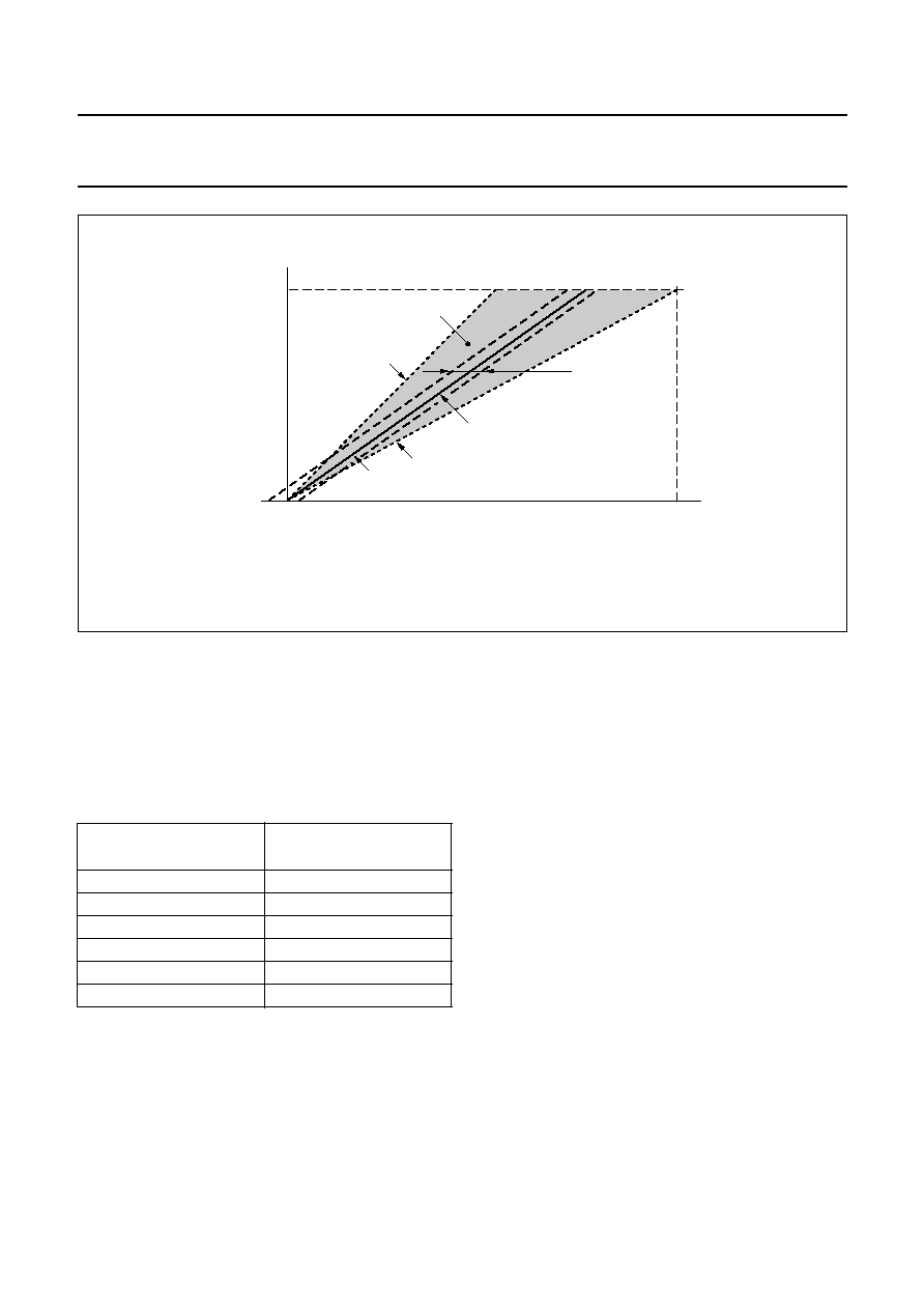
Fig.9 Slave input data transferring speed.
(1) Ideal frame transfer characteristics are restricted to this area.
(2) Ideal frame transfer characteristic (example).
handbook, full pagewidth
MGE476
slope = CDCL frequency
slope = input bit rate
(2)
jitter limits
slope = maximum
CDCL frequency
Nf
transferred
input bits
0
0
time
Tf
(1)
The shaded area in Fig.9 represents the restrictions to the
transfer characteristic of a frame. The characteristic may
not cross the shown upper limit of the shaded area in order
to prevent input buffer underflow and/or overflow.
The slope of the upper limit is determined by the sample
frequency as shown in Table 5.
Table 5
Slope of the upper limit determined by sampling
frequency
SAMPLE FREQUENCY
(kHz)
MAXIMUM CDCL
FREQUENCY (kbits/s)
48
768
44.1
705.6
32
512
24
384
22.05
352.8
16
256
1997 Nov 17
15
Philips Semiconductors
Preliminary specification
ISO/MPEG Audio Source Decoder
SAA2502
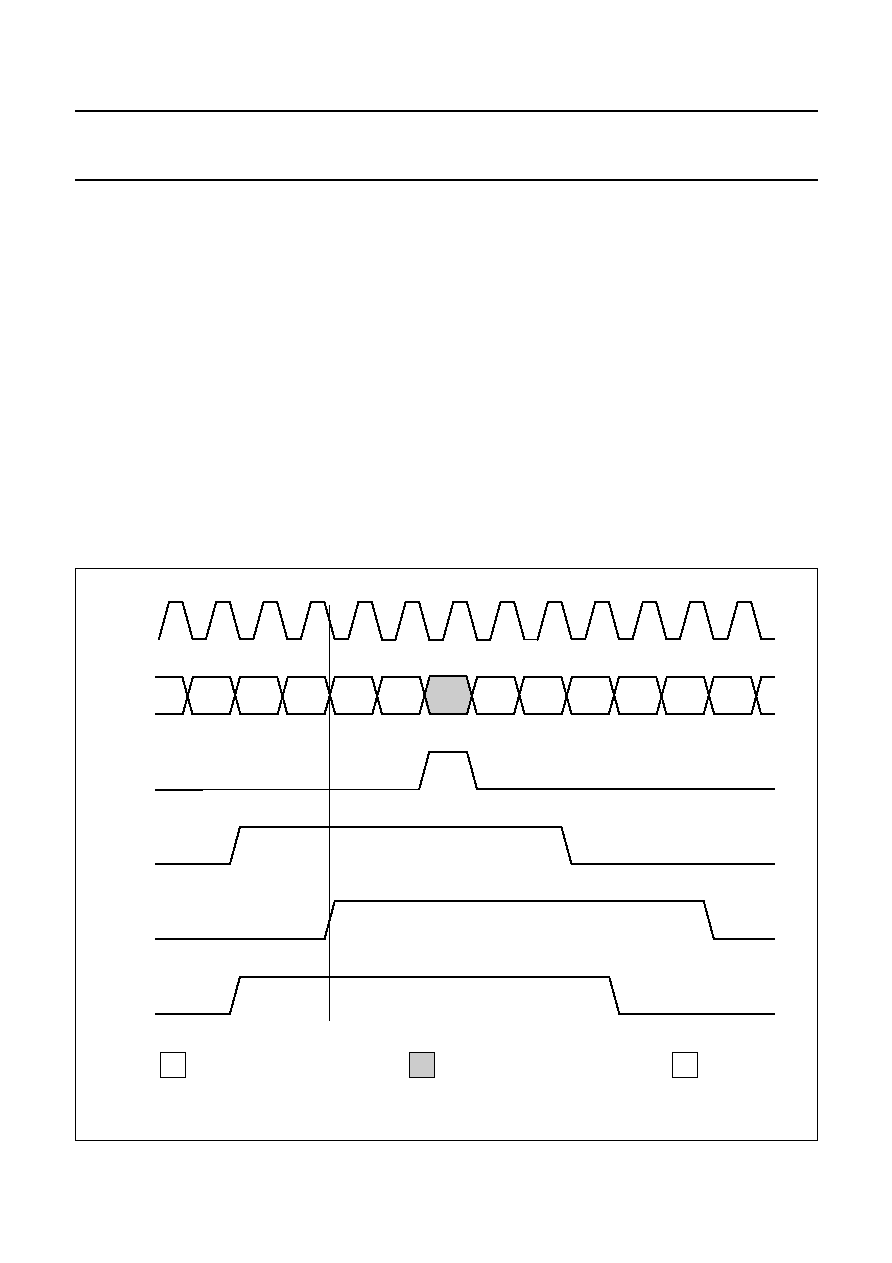
7.3.3
B
UFFER CONTROLLED INPUT MODE
(see Fig.10)
Buffer controlled input mode is activated by setting the
INMOD control flags to 1X, which means that the SAA2502
will request data based on the amount of input bytes
currently residing in the input buffer.
The bit clock CDCL is output, its frequency is fixed:
when MCLK24 = logic 1
when MCLK24 = logic 0.
In this mode CDRQ = logic 1 is an indication that new input
data is required. CDVAL = logic 1 indicates the delivery of
valid data. The application should react to the event of an
input data request as follows:
∑
One byte of input data should be delivered within
16 CDCL cycles. If CDRQ remains high the next byte
MCLK
32
------------------
MCLK
16
------------------
should be delivered and so on until CDRQ is dropped.
Delivery of subsequent bytes while CDRQ remains
HIGH should be uninterrupted (CDVAL should stay
HIGH)
∑
There is also an option for the application to deliver part
of the input data later. Despite violating the conditions in
the previous paragraph, this is allowed, but with
consequences for the input buffer latency time.
MPEG free format bit rate is allowed in this mode.
Dynamically varying bit rate may be supported in this
mode. Whether such support is desired or not is indicated
by the following input mode bits:
∑
INPMOD = 10 means bit rate is assumed to be (quasi)
static
∑
INPMOD = 11 means bit rate is assumed to be dynamic.
Fig.10 Buffer controlled mode input data format.
,,,
,,,
,,
,,
,,
,,
,,
,,
,,
,,
,,
,,
handbook, full pagewidth
MGE477
CDCL
CD
CDEF
CDRQ
CDVAL
CDSY
unreliable data bit (example)
start of byte or frame
valid data
valid but unreliable data
invalid data
,,
,,

1997 Nov 17
16
Philips Semiconductors
Preliminary specification
ISO/MPEG Audio Source Decoder
SAA2502
7.4
Decoder core
The SAA2502 fully complies with MPEG1 (layer I and II)
and MPEG2 (layer I and II, L
0
and R
0
channels). Also
some DAB specific features are supported. Free format bit
rate is not supported in master input mode. Several
aspects of the decoding process and audio
post-processing features are offered.
7.4.1
F
RAME SYNCHRONIZATION TO INPUT DATA STREAMS
The SAA2502 has to localize the start of a frame before
decoding may begin. The process of locating the start of a
frame is called frame synchronization. There are
4 different modes of frame synchronization available.
These modes are in order of decreasing speed of frame
synchronization.
7.4.1.1
Frame sync pulse mode
In this mode the start of each frame is marked by a rising
edge of the CDSY input pin. It is the fastest and most
reliable method of frame synchronization. It is activated by
loading 11 into the SYMOD control flags.
7.4.1.2
Byte aligned mode
This default mode may also be enforced by loading 10 into
the SYMOD control flags. The start of a frame is located by
detection of the 14-bit sync pattern 111111111111X1.
The probability of correct sync detection is enhanced by
the fact that a rising edge of the CDSY input pin marks a
location which is byte aligned with frame bounds. A rising
edge of CDSY is not required at every byte edge but
should occur at regular intervals for reliable frame
synchronization.
7.4.1.3
Layer II non-byte aligned mode
This mode may be entered by loading 01 into the SYMOD
control flags. Frame start is found by detection of the 15-bit
sync pattern 111111111111X10.
As this pattern is slightly longer than the previous one and
also contains at least one 1-to-0 transition, it may be used
to obtain frame synchronization in the absence of any
external alignment indication (CDSY is ignored and
therefore may be left floating).
7.4.1.4
General non-byte aligned mode
This mode may be entered by loading 00 into the SYMOD
control flags. Frame start is detected by alternating
searches for a 15-bit sync pattern 111111111111X10
(identical to the layer II mode search pattern) and a15-bit
sync pattern 0111111111111X1.
Because valid MPEG streams exist that do not contain the
first pattern while other valid MPEG streams do not contain
the second pattern a time-out counter will always be active
in this mode. Time-out length is set to slightly more then
72 ms which is the length of the longest audio frame.
The second pattern operates for layer I and layer II, but
successful synchronization is only guaranteed when the
last bit of the previous frame equals logic 0. Consequently
this mode synchronizes to layer I input bit streams only if
frames at least sometimes end with a logic 0 bit. Both
patterns contain the 1-to-0 or 0-to-1 transition required for
a reliable start-of-frame detection in the absence of
external alignment information.
If the SAA2502 starts at a random place in the bit stream,
it may take up to one frame before a sync pattern or sync
pulse is encountered. Because sync patterns may be
emulated by frame content, detection of a sync is always
followed by a verification period to check whether the sync
is located at the start of a frame. The length of the
verification period depends on the presence of CRC
protection and/or a free format bit rate index. During sync
search and verification the baseband audio outputs are
muted. If verification fails the synchronization process is
restarted.
Table 6
Frame sync verification
INPUT DATA FORMAT
LENGTH OF VERIFICATION PERIOD
FREE FORMAT BIT RATE
NON-FREE FORMAT BIT RATE
MPEG; no CRC
2 frame bit rate
1 frame
MPEG with CRC
1 frame
0 frame
1997 Nov 17
17
Philips Semiconductors
Preliminary specification
ISO/MPEG Audio Source Decoder
SAA2502
7.4.2
M
ASTER INPUT MODE BIT RATE GENERATION
When master input mode is used, the SAA2502 fetches
input data at the effective bit rate. However after a hard
reset the input requests input data at the default bit rate
until synchronization has been established as shown in
Table 7.
When the clock generator mode is `free running internal
sample clock' or `locked internal sample clock' the default
input bit rate is always 384 kbits/s. When the mode is
`external sample clock' the SAA2502 derives the selected
bit rate from the signal FSCLKIN. But initially it has no
indication of the current sampling rate corresponding to
FSCLKIN. Therefore the bit rate of 384 kbits/s is
generated at an assumed sampling frequency of 44.1 kHz.
For different sample rates, the bit rate changes
proportionally.
The consequence is that while the SAA2502 is
synchronizing after a hard reset, the application should be
able to supply input data at the given default bit rate until
synchronization is established. Alternatively there is also
the possibility to overrule default bit rate setting and
sample rate setting using the control interface while
synchronization has not been established.
The speed at which input data is requested by the input in
master mode is changed in one of the following events:
∑
When input synchronization is established at the end of
the verification phase and the bit rate index of the
decoded bit stream indicates a bit rate different from the
one currently selected. In this event, the bit rate is
adapted to the new index.
∑
When the signal STOP is raised while the STOPRQ
control flag = logic 1, input requesting is halted.
Requesting resumes at the last selected input bit rate
when the STOP signal is dropped.
In all other events (including when the SAA2502 loses
synchronization), the last selected input bit rate is
maintained.
Whenever the selected bit rate changes while dynamic bit
rate is not enabled, the SAA2502 will generate internally a
soft reset resulting in a soft mute of the output interfaces
and a decoder restart in order to re-initialize internal buffer
settings.
Table 7
Establishment of default bit rate
CLOCK GENERATOR MODE
FSCLKIN (kHz)
DEFAULT BIT RATE (kbits/s)
Free running internal clock
don't care
384
Locked internal clock
don't care
384
External sample clock
256 or 384
◊
48
417.96
256 or 384
◊
44.1
384
256 or 384
◊
32
278.64
256 or 384
◊
24
208.98
256 or 384
◊
22.05
192
256 or 384
◊
16
139.32

1997 Nov 17
18
Philips Semiconductors
Preliminary specification
ISO/MPEG Audio Source Decoder
SAA2502
7.4.3
S
AMPLE CLOCK GENERATION
When the `external sample clock' mode of the clock
generator is used, the application must know the sample
rate. FSCLKIN has to be applied, with a frequency which
is a multiple of the sample rate. The (sample rate
dependent) output interface timing signals will be
generated from FSCLKIN. This mode will normally be
used in applications with a fixed sample rate. Should the
sample rate change, then a soft reset is strongly advised.
When one of the remaining clock generator modes is used,
the SAA2502 selects the active sample rate automatically,
and generates the required sample rate related timing
signals from its MCLKIN and X22IN clock inputs. Soft
resets at sample rate changes are generated
automatically. After a hard reset, a sample rate of 44.1 kHz
by default is selected. Such default setting may be
overruled using the control interface.
SCK, WS and SPDIF will show frequency changes in any
of the following 3 situations:
∑
When the SAA2502 establishes synchronization to the
coded data input bit stream at a sample rate different
from the one previously selected
∑
When the current (default) sample rate is overruled by
the control interface
∑
When the clock generator mode is changed, resulting in
a switch from or to the `external sample clock mode.
In all those situation the phase of WS and the data content
of SPDIF will be continuous.
In all other events SCK, WS and SPDIF remain operating
without phase or frequency changes and the sample rate
selection remains unchanged.
7.4.4
D
ECODER PRECISION
During decoding several multiply operations are carried
out on coded samples. The results of these operations
have to be rounded in order to keep the word length
required for internal number representation within
reasonable limits. Accumulation of these rounding errors is
kept at a very low level in order to assure precise audio
output samples. SAA2502 precision is specified using the
output of the MPEG reference decoder based on double
precision floating point calculations as a reference.
Differences between that reference decoder and SAA2502
output manifest themselves as white noise.
Two contributions to this noise may be identified:
∑
Noise resulting from internal rounding on intermediate
results
∑
Noise resulting from rounding of final output samples
to 16, 18, 20 or 22 bits (depending on selected output
accuracy).
Table 8 shows the effective noise level figures. (unit is
1 LSB of 22-bit accuracy output). Except for 22-bit
accuracy, output rounding is by far the dominant effect.
Consequently the SAA2502 may be considered a
professional level high precision decoder.
Table 8
Effective noise level figures
Note
1. The output rounding part of this precision is valid only for I
2
S and SPDIF outputs.
OUTPUT ACCURACY
(BITS)
INTERMEDIATE
ROUNDING
OUTPUT ROUNDING
(1)
TOTAL NOISE LEVEL
22
0.6
0.3
0.7
20
0.6
1.2
1.3
18
0.6
4.6
4.7
16
0.6
18.5
18.5

1997 Nov 17
19
Philips Semiconductors
Preliminary specification
ISO/MPEG Audio Source Decoder
SAA2502
7.4.5
S
CALE FACTOR
CRC
PROTECTION
MPEG specifies an optional 16 bit CRC that may be used
to verify whether an important part of each audio frame is
received correctly. The following data items is protected by
this CRC:
∑
Bytes 3 and 4 of the first 4 bytes of each frame,
containing most of the frame header information
∑
Allocation information
∑
Scale factor select information (layer II only).
The scale factors are not protected by this scheme.
The DAB specification includes CRC protection for scale
factors. The 32 sub-bands are divided into the following
4 blocks:
Block 0 = sub-bands 0 to 3
Block 1 = sub-bands 4 to 7
Block 2 = sub-bands 8 to 15
Block 3 = sub-bands 16 to 31.
Each block is protected by an 8-bit CRC if that block of
sub-bands is (partly) inside the current sub-band limit.
The required scale factor CRCs are stored in the last bytes
of the previous audio frame:
∑
The last two bytes of each frame are reserved for
ancillary data; DAB specification calls this Fixed
Program Associated Data (FPAD)
∑
Minimum 2 and maximum 4 bytes before FPAD are
reserved for scale factor CRCs. The number of CRC
bytes present is be derived from the sub-band limit of the
following audio frame
∑
Bytes before the CRCs are available for more ancillary
data; DAB specification calls this extended Program
Associated Data (XPAD), as far as not occupied by
MPEG coded input data.
The DAB type of scale factor CRC protection, extended to
all valid sample frequency plus bit rate combinations of
MPEG1 and MPEG2, and to layer I, is fully supported by
the SAA2502. (DAB is restricted to MPEG1 layer II, to
48 kHz sample frequency and does not support free
format bit rate). Requirements for scale factor CRC
handling is indicated by the SFCRC control flag.
7.4.6
H
ANDLING OF ERRORS IN THE CODED INPUT DATA
The SAA2502 is able to handle certain types of errors in
the input data. Three error categories will be handled:
∑
Errors flagged by the coded input data error flag CDEF
∑
CRC failures (if MPEG and/or scale factor error
protection is active)
∑
MPEG audio frame syntax errors.
Error flags in the input data will effect the decoding process
if the corrupted data is inside the header, bit allocation or
scale factor select information part of a frame (then the
SAA2502 will `soft' mute that frame) or inside the scale
factor field (then the most recent valid scale factor of the
same sub-band will be copied).
Error flags in other data fields will be ignored. If MPEG
and/or scale factor CRCs are active the CRC result has
priority over CDEF flags inside the protected fields. In
applications where the MPEG CRC is always present, the
protection bit (which is not CRC protected) in the MPEG
header may be overruled by setting control flag CRCACT.
Thus the SAA2502 is robust for data errors in the
protection bit.
1997 Nov 17
20
Philips Semiconductors
Preliminary specification
ISO/MPEG Audio Source Decoder
SAA2502
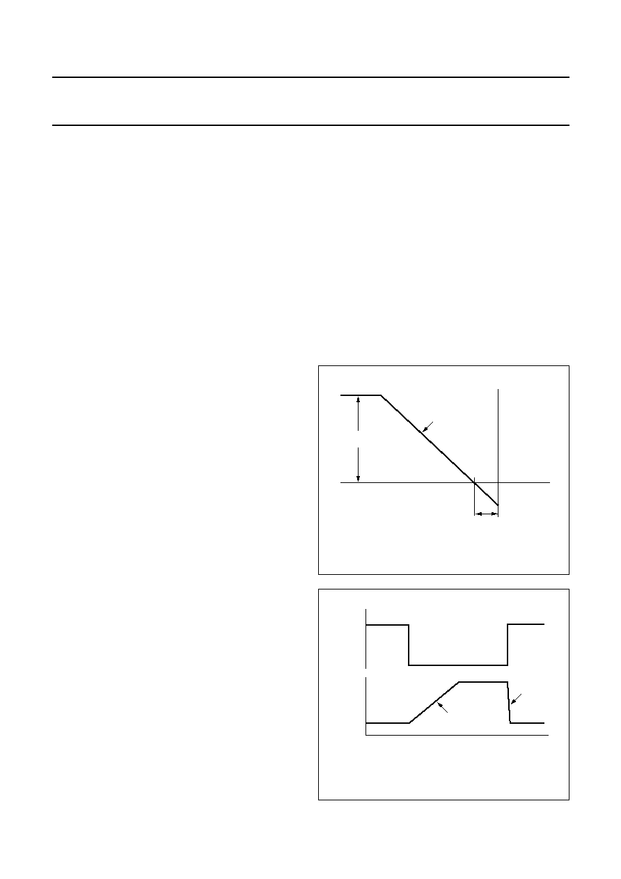
7.4.7
D
YNAMIC RANGE COMPRESSION
The baseband audio output resulting from MPEG
decoding has a high dynamic range (theoretically
>200 dB, practically up to 120 dB for the 22-bit output
mode).This feature is very attractive from the high quality
audio standpoint of view, but such high dynamic range is
undesirable when there is a relatively high level of
background noise (e.g. for car radio). For those
applications the SAA2502 offers the possibility of built in
dynamic range compression:
∑
Internal dynamic range compression is offered. Thus
any standard MPEG encoded bit stream may be
compressed i.e. no added compression information is
required.
∑
The dynamic range compression algorithm is fully
parameterised. All major characteristics are
programmable through the control interface:
≠ Level of compression
≠ Maximum compression
≠ Compression offset
≠ Compression release rate (compression attack rate
has to be fixed).
The dynamic range compression algorithm is based on a
(in time varying) amplification factor, which is equally
applied to all audio output samples. The value of the
amplification factor is calculated on basis of the current
audio output power level for each (sub)frame of 384 output
samples. The applied power to amplification curve is
shown in Fig.11. All characteristics of the curve are
programmable:
∑
Compression slope minimum = 0, maximum = 0.996
∑
Maximum amplification minimum = 0 dB,
maximum = 23.81 dB
∑
Offset minimum = 0 dB, maximum = 47.81 dB.
Offset values close to 0 dB may result in clipped output
signals. This is especially true for signals with a high
amplitude-to-power ratio (an extreme example of such a
signal is a maximum amplitude unit impulse).
The occurrence of this effect can be avoided by selecting
an offset value close to or greater than 15 dB.
In the context of dynamic range compression definition,
the 0 dB power reference level is defined as a sine wave
shaped output signal with maximum amplitude in just one
(right or left) channel.
The calculation will result in an new amplification factor
every 384 samples (i.e. from 8 ms at 48 kHz to 24 ms at
16 kHz sample rate). Subsequent amplification factors
may vary considerably.
An example showing two large step type discontinuation is
shown in Fig.12. It is undesirable to apply large increasing
amplification steps immediately. Consequently increasing
the amplification factor is limited to the `release rate' which
is also programmable:
∑
Minimum release rate =
(1.46 dB/s at 48 kHz; 0.488 dB/s at 16 kHz)
∑
Maximum release rate =
(46.87 dB/s at 48 kHz; 15.625 dB/s at 16 kHz).
Decreasing amplification factors, must be applied almost
immediately to avoid overflow when the audio power
increases rapidly; thus attack rate is non-programmable
and fast.
0.0117 dB
384 samples
----------------------------------
0.375 dB
384 samples
----------------------------------
Fig.11 Dynamic range compression characteristic.
handbook, halfpage
MGE478
maximum
amplification
compression
slope
amplification
(dB)
0 dB
power (dB)
offset
Fig.12 Amplification change rates.
handbook, halfpage
MGE479
audio
signal
power
amplifi-
cation
release
rate
attack
rate
time

1997 Nov 17
21
Philips Semiconductors
Preliminary specification
ISO/MPEG Audio Source Decoder
SAA2502
7.4.8
B
ASEBAND AUDIO PROCESSING
Baseband audio de-emphasis as indicated in the MPEG
input data stream is performed digitally inside the
SAA2502. The included `Audio Processing Unit' (APU)
see Fig.19, may be used to apply programmable
inter-channel crosstalk or independent channel volume
control.
The APU attenuation coefficients LL, LR, RL and RR may
be changed dynamically by the microcontroller, writing
their 8-bit indices to the SAA2502 through its control
interface. The coefficient changes become effective within
one sample period after writing. To avoid audible clicks at
coefficient changes, the transition from the current
attenuation to the next is smoothed. The relationship
between the APU coefficient index and the actual
coefficient (i.e. the gain) is shown in Fig.14 and in Table 9
For coefficient index 0 to 64 the step size is
-
3
/
16
dB and
for coefficient index 64 to 255 the step size is
-
3
/
8
dB.
The APU has no built-in overflow protection, so the
application must assure that the output signals of the APU
cannot exceed the 0 dB level. For an update of the APU
coefficients, it may be required to increase some of the
coefficients and decrease some others. The APU
coefficients are always written sequentially in a fixed
sequence LL, LR, RL and RR. Therefore, to prevent
(temporary) internal APU data overflow, the following
sequence of steps may be necessary:
1. Write LL, LR, RL and RR, but change only decreasing
coefficients. Overwrite increasing coefficients with
their old value (therefore do not change these yet).
2. Write LL, LR, RL and RR again, but now change
increasing coefficients, keeping the other ones
unchanged.
Table 9
APU coefficient index and actual coefficient.
APU COEFFICIENT INDEX C
APU
COEFFICIENT
BINARY
DECIMAL
00000000 to 00111111
0 to 63
01000000 to 11111110
64 to 254
11111111
255
0
2
C
32
------
≠
2
C
32
≠
(
)
16
-----------------------
≠
Fig.13 Audio Processing Unit (APU).
handbook, halfpage
left decoded
audio
samples
LR
LL
RL
left output
audio
samples
right decoded
audio
samples
RR
right output
audio
samples
MGB493
Fig.14 Relation between APU coefficient index and
gain.
(1) Step
-
3
/
16
dB per coefficient increment.
(2) Step
-
3
/
8
dB per coefficient increment.
handbook, halfpage
MGE480
0
0
-
12
-
83.25
254 255
(2)
(1)
APU coefficient index
gain
(dB)
64
1997 Nov 17
22
Philips Semiconductors
Preliminary specification
ISO/MPEG Audio Source Decoder
SAA2502
7.4.9
D
ECODER LATENCY TIME
Latency time is defined as elapsed time between the
moment that the first byte of an audio frame is delivered to
the SAA2502 and the moment that the output response
resulting from the first (sub-band) sample of the same
frame reaches its maximum.
Latency time results from the addition of two internal
latency contributions: t
latency
= t
proc
+ t
buf
.
∑
The processing latency time (t
proc
) is sample frequency
dependent (see Table 10).
∑
The input buffer latency time (t
buf
) is input interface
mode dependent.
Precision of latency time calculation is sampling rate and
bit rate dependent. Maximum deviation is roughly plus or
minus 4 sample periods.
7.4.9.1
Master and slave input interface modes
Input buffer latency time t
buf
= (minimum of t
buf1
and
t
buf2
) + cr
◊
3.52 ms:
∑
t
buf1
is sample frequency dependent (see Table 10)
∑
t
buf2
is input bit rate dependent (see Table 11 and
Table 12)
∑
cr is the ratio between maximum and actual value of
MCLKIN frequency.
For slave input interface mode NOT the average input bit
rate should be used for table look-up, but CDCL frequency
(input bit rate during the burst). For free format bit rates the
table should be interpolated (t
buf2
is proportional to
1/bit rate).
Table 10 Processing latency time
SAMPLE FREQUENCY
(kHz)
t
proc
(ms)
t
buf1
LAYER I (ms)
t
buf1
LAYER II (ms)
48
6.67
8.00
24.00
44.1
7.26
8.71
26.12
32
10.00
12.00
36.00
24
13.33
16.00
48.00
22.05
14.51
17.41
52.24
16
20.00
24.00
72.00
Table 11 Buffer latency time; high bit rate
BIT RATE (kbits/s)
t
buf2
(ms)
448
5.52
384
6.44
320
7.73
256
9.66
192
12.88
160
15.45
128
19.31
96
25.75
64
38.63
48
51.50
32
77.25
16
154.50
Table 12 Buffer latency time; low bit rate
BIT RATE (kbits/s)
t
buf2
(ms)
416
5.94
352
7.02
288
8.58
224
11.04
176
14.05
144
17.17
112
22.07
80
30.90
56
44.14
40
61.80
24
103.00
8
309.00
1997 Nov 17
23
Philips Semiconductors
Preliminary specification
ISO/MPEG Audio Source Decoder
SAA2502
7.4.9.2
Buffer controlled input mode
Input buffer latency time behaviour is relatively complex in
this mode.
At start-up (i.e. during the search-for-frame sync) latency
time is very small (t
buf
< 2 ms) because the input buffer
remains empty.
After a frame sync is detected, normal decoding starts and
the buffer fills up to its desired fill level. That level will result
in a buffer latency time t
buf2
(see Tables 11 and 12, t
buf1
plays no role) for constant bit rate operation.
It is more complex for variable bit rates, at high bit rates the
buffer will hold only a fraction of a frame, while at low bit
rates it may hold many frames (each possibly of a different
bit rate). Also input buffer content may deviate from the
desired level because data consumption rate at the output
of the buffer may be high during short periods while
replenishing is limited by CDCL frequency.
As a result buffer latency time in buffer controlled input
mode may be predicted more or less accurately only at
(re)start time.
Another consequence of buffer behaviour at very low bit
rates in this mode is that buffer latency time values may
become large. Therefore it might be possible that the
SAA2502 will request data, which is not (yet) available.
In those situations the SAA2502 is requesting more data
than required; storage of more than one complete frame in
the input buffer is never necessary.
Consequently the application may delay delivery of
requested data until it becomes available without any
effect on correct SAA2502 operation. This option
constitutes delayed delivery possibility.
7.5
Output interface module
The output interface module produces stereo baseband
output samples in three different formats at the same time:
∑
I
2
S
∑
SPDIF
∑
256 times oversampled bit serial analog.
Any of the three outputs may be enabled or disabled in
order to save dissipation and minimize EMC generation in
applications that do not need all of them.
Decoded mono streams and the (user) selected channel of
dual channel streams are presented at both (left and right)
output channels.
If indicated in the coded input data, de-emphasis filtering
is performed digitally on the output data, thus avoiding the
need of external analog de-emphasis filter circuitry.
7.5.1
I
2
S
OUTPUT
This output interface section generates decoded
baseband audio data in I
2
S format (see Fig.15).
The I
2
S output interface section consists of 3 signals
(see Table 13).
Fig.15 I
2
S output serial data transfer format.
handbook, full pagewidth
WS
SCK
SD
MSB
left sample
LSB
MSB
right sample
LSB
1
16/18/20/22
32
1
16/18/20/22
32
valid data
MGB502

1997 Nov 17
24
Philips Semiconductors
Preliminary specification
ISO/MPEG Audio Source Decoder
SAA2502
Table 13 Signals of output interfacing
The frequency of clock SCK is 64 times the sample
frequency.
The signal SD is the serial baseband audio data, sample
by sample (left/right interleaved; the left sample and the
right immediately following it form one stereo pair). 32 bits
are transferred per sample per channel. The samples are
transmitted in two's complement, MSB first. The output
samples are rounded to either 16, 18, 20 or 22 bit
precision, selectable by the control interface flags RND1
and RND0. The remainder of the 32 transferred bits per
sample per channel are zero.
The word select signal WS indicates the channel of the
output samples (LOW if left, HIGH if right).
7.5.2
SPIDF
OUTPUT
7.5.2.1
SPIDF format
The SPDIF data format is frame based. One SPDIF frame
represents one audio sampling period. Complete frames
must be transmitted at the audio sample rate. Every frame
comprises two sub-frames, each of 32 bits. The data is
transmitted in bi-phase mark modulated format to ensure
a zero DC component.
Four bits of data at the beginning of each sub-frame are
assigned to frame and sub-frame synchronization, which
is achieved using a set of 3 output sequences which
violate the bi-phase mark rules. The audio samples
occupy 24 bits (bits 4 to 27), transmitted LSB first.
Depending on the selected accuracy the 2, 4, 6 or 8 LSBs
will be logic 0.
Bits 28 to 31 are occupied by the validity flag for the audio
sample, a channel status bit (each super-frame of
192 frames contains two groups of 192 channel status
bits, one for each channel), a user data bit, and a parity bit
(even parity for bits 4 to 31). These bits are described
respectively as V, U, C and P in the SPDIF specification.
The synchronization for the channel status frame is
achieved by a pair of preamble violation sequences.
The synchronization for the user channel data is
embedded within the data.
SIGNAL
DIRECTION
FUNCTION
SCK
output
data clock
SD
output
baseband audio data
WS
output
word select
7.5.2.2
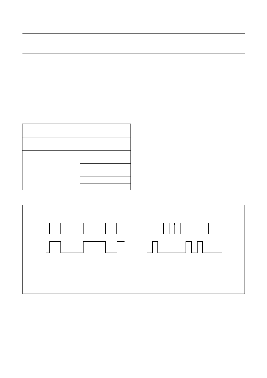
Frame synchronization patterns (Bits 0 to 3,
SPDIF subframe)
The frame synchronization patterns are based on bi-phase
violations. They are sent as shown in Table 14
The sequences are sent in place of 4 bi-phase coded
bits 0 to 3. They are not bi-phase coded, but are sent as
they are.
Table 14 Frame synchronization patterns
7.5.2.3
Validity flag (bit 28, SPDIF subframe, V bit)
The V bit is intended to indicate an invalid data sample.
Equipment connected to the interface is expected to
perform interpolations across small numbers of invalid
(V = logic 1) samples. Owing to the manner in which data
is decoded in the SAA2502, and the sub-band processing
of the signal, an input data error affects output audio
signals in a complex way.
There is not a simple relationship between input errors and
damaged audio samples. Therefore the validity flag value
is made programmable (through the control interface unit)
Control software can use this bit in any way required.
7.5.2.4
User channel data (bit 29, SPDIF subframe,
U bit)
There is a single user data channel. Two bits of data in this
channel are transmitted in each frame. For this minimum
implementation only the possibility to send single byte user
messages to the user channel is offered. Each byte sent
will be preceded by a single logic 1 valued start bit.
The 8 bits of the user message are then sent LSB first.
7.5.2.5
Channel status data (bit 30, SPDIF sub-frame,
C bit)
A group of C channel status bits consists of 192 bits.
Two groups of channel status bits are transmitted every
super-frame (one group for each channel) at a rate of one
bit per sub-frame. In this application, both channel status
words will be identical.
BINARY
PATTERN
DESCRIPTION
11101000
B
left sub-frame follows.
SPDIF super-frame starts.
Bit 0 of left C channel will
be sent in this subframe
11100100
W
right subframe follows
11100010
M
left subframe follows
1997 Nov 17
25
Philips Semiconductors
Preliminary specification
ISO/MPEG Audio Source Decoder
SAA2502
Table 15 Channel status data
Notes
1. This field is filled according to clause 4.2.2.2 of the SPDIF standard `Channel status data format for digital audio
equipment for consumer use' (mode 0).
2. The low sample frequencies of MPEG2 are not defined yet. In order to be able to follow future standardization, the
code sent for the three remaining sampling frequencies (24, 22.05 and 16 kHz) is programmable through the
controller interface.
3. The remaining 162 bits of each channel status word will all be logic 0. Individual bits of the status channel will be sent
bit 0 first.
DESCRIPTION
BITS
FIELD
INDICATION
Control field; note 1
0
0
indicates consumer use
1
0
logic 1 reserved for digital data and further
standardization
2
C
logic 0 = copy prohibited; logic 1 = copy permitted
3 and 4
00
no pre-emphasis (SAA2502 has automatic
de-emphasis)
5
0
2 channel audio data
6 and 7
00
mode 0 indication
Category code
8 to 15
00000000
2 channel
Source number
16 to 19
0000
don't care
Channel number
20 to 23
0000
don't care
Sample frequency;
note 2
24 to 27
field filled in accordance with clause 4.2.2.2 of the SPDIF standard:
0100 = 48 kHz
0000 = 44.1 kHz
1100 = 32 kHz
Clock accuracy; note 3
28 and 29
field filled in accordance with clause 4.2.2.2 of the SPDIF standard:
00= level II (normal accuracy of 0.1%)
7.5.2.6
Parity (bit 31, SPDIF sub-frame, P bit)
Even parity is generated on the 28 sub-frame data bits
(4 to 31) in bit 31.
7.5.2.7
SPDIF control
The SPDIF interface will be controlled by the
microcontroller via the control interface. The V bit is copied
into each SPDIF subframe (once for each data sample).
The C bit is inserted twice per SPDIF super-frame into the
channel status data (bit 2 in each C channel). The user
byte is inserted into the user channel (preceded by a start
bit) immediately after reception through the control
interface, otherwise the user channel is filled with logic 0s.
Table 16 SPDIF interface control
7.5.2.8
Channel status
The sampling frequency bits (bits 24 to 27) are derived
from the sampling frequency index bits of the input data
stream
7.5.2.9
User data
Only single 8 bit messages are sent. Individual messages
should be time separated far enough to insert at least
9 logic 0s in between (for easy synchronization at the
receiver end at random entry points in the stream).
BIT/BYTE
DEFAULT
RESULT
V bit
default = logic 0
valid audio data
C bit
default = logic 1
digital copy permitted
U byte
uuuuuuuu
8 bits user byte
1997 Nov 17
26
Philips Semiconductors
Preliminary specification
ISO/MPEG Audio Source Decoder
SAA2502
7.5.3
B
IT SERIAL ANALOG OUTPUT
In order to serve applications which require low to medium
performance stereo audio output, two bit serial analog
outputs are provided (one for each channel). The on-chip
DACs each consist of three functional blocks in series:
∑
4
◊
f
s
up-sampling filter
∑
AC and DC dithering block
∑
N
◊
f
s
noise shaper; see Table 17.
Table 17 Value of N for N
◊
f
s
noise shaper
MODE
SAMPLE
RATE
VALUES
External sample clock mode
FSC384 = 0
N = 256
FSC384 = 1
N = 384
Other clock generator modes f
s
= 48 kHz
N = 256
f
s
= 44.1 kHz
N = 256
f
s
= 32 kHz
N = 384
f
s
= 24 kHz
N = 512
f
s
= 22.05 kHz N = 512
f
s
= 16 kHz
N = 768
The two analog outputs deliver a `pulse density modulated'
signal, switching between REFN and REFP. The format is
programmable (through the control interface):
∑
Non return-to-zero format (subsequent logic 1 pulses
are merged)
∑
Return-to-zero format (subsequent logic 1 pulses are
separated by logic 0 levels).
The quality of the analog output signal depends on several
external factors:
∑
Stability and decoupling of the analog supply
∑
Absence of jitter on the sample clock
∑
Which external low-pass filter circuit is used
∑
The layout of the low-pass filter.
The recommended external low-pass filter is shown in
Fig.17. With this circuit the DACs performance is <
-
75 dB
(THD + N)/S with a 1 kHz sine wave, measured over the
bandwidth 20 Hz to 20 kHz. The amplifier in the low-pass
filter circuit is the Class AB stereo headphone driver
TDA1308.
The recommended DAC output format is non
return-to-zero, this has a better signal-to-noise ratio than
the return-to-zero format.
Fig.16 Bit serial output formats.
handbook, full pagewidth
MGE481
LFTPOS
RGTPOS
LFTNEG
RGTNEG
bit serial data
0
1
1
0
0
1
0
1
1
0
0
1
non-return-to-zero
(recommended)
return-to-zero
1997 Nov 17
27
Philips Semiconductors
Preliminary specification
ISO/MPEG Audio Source Decoder
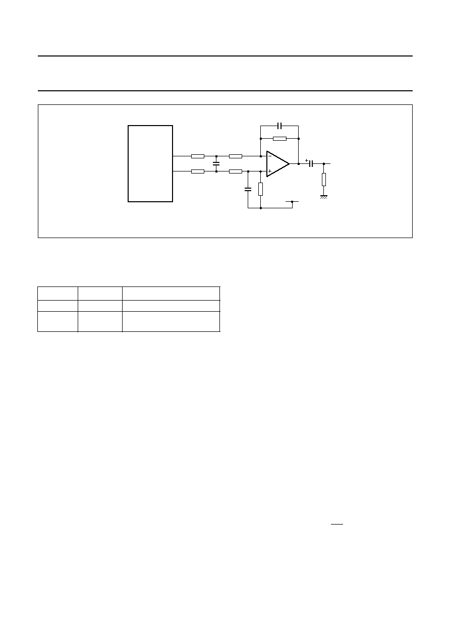
SAA2502
handbook, full pagewidth
MBH974
220 pF
+
2.5 V
220 pF
390 pF
TDA1308T
SAA2502H
neg
pos
output
11 k
10 k
10 k
10 k
10 k
100
µ
F
11 k
10 k
Fig.17 External low-pass filters
7.6
Control interface module
7.6.1
R
ESETTING
Table 18 Resetting is performed by 2 signals
A rising edge of the signal STOP triggers the next event.
The decoding process is interrupted and the input buffer is
flushed. Consequently audio frame synchronization is
abandoned and the decoder starts searching for a new
sync in the coded input data stream. In the meantime the
output interface is soft muted (i.e. the output signal fades
away in approximately 500 samples).
There are several other events that have the same effect
as a rising edge of the STOP signal:
∑
Change of the current MPEG layer in the input stream
∑
Change of the current sampling frequency in the input
stream
∑
Change of the current bit rate in the input stream
(variable bit rate is NOT supported)
∑
Change of current input interface mode
(INMOD1 and 0) and/or audio frame synchronization
mode (SYMOD1 and 0) setting
∑
Enforcement of a soft reset through the control interface.
There is also a level triggered effect which remains
provided STOP is asserted. When the STOPRQ control
flag is set input data requesting will be halted, otherwise
normal input interface behaviour will continue at the bit rate
that was valid before STOP assertion but all data is
SIGNAL
DIRECTION
FUNCTION
STOP
input
soft reset and stop decoding
RESET
input
hard reset: force default
settings
considered to be unreliable (as if CDEF were asserted).
Consequently frame synchronization and decoding will not
resume until STOP is de-asserted.
The hard reset signal RESET has the same effect as
STOP but it will also force the control interface settings into
their default states. RESET must stay high during at least
24 MCLKIN periods if MCLK24 = logic 1 or 12 MCLKIN
periods if MCLK24 = logic 0.
7.6.2
I
NTERRUPTS
The SAA2502 is able to generate an interrupt upon the
occurrence of one or more of the following events:
∑
Status bit DST0 has been set (i.e. ancillary/PAD data,
frame headers and error report are available)
∑
Rising edge of STOP input signal
∑
MPEG CRC check failed
∑
Status bit INSYNC has been set
∑
Status bit INSYNC has been cleared.
For more information on these items see Sections 7.6.6.1
and 7.6.6.9.
Each of these interrupts sources may be enabled or
disabled as required by the application. After a hard reset
all interrupt sources are disabled. When the host
processor is interrupted by the SAA2502 it should read the
interrupt event register to find out which event or events
caused the interrupt. Reading this register will also clear all
pending interrupts.
The interrupt pin is active LOW (INT = logic 0 indicates an
interrupt) and it is of the `open drain' type. Consequently it
is allowed to `wire OR' this pin with interrupt pins of the
same type of other devices. For correct operation an
external pull-up resistor should be provided.
1997 Nov 17
28
Philips Semiconductors
Preliminary specification
ISO/MPEG Audio Source Decoder
SAA2502
7.6.3
M
ICROCONTROLLER INTERFACE
The microcontroller interface operates in one of two distinct modes of operation: L3 or I
2
C-bus. Mode setting is
determined at initialization. The interface uses 3 signals. The function of these signals in the two modes is indicated in
Table 19:
Typical advantages of the use of the L3 protocol are:
∑
High speed protocol (normally the speed of the microcontroller will be the limiting factor)
∑
The protocol may be implemented using microcontrollers featuring only standard I/O ports.
The implemented I
2
C-bus interface is of the 400 kbits/s, 7-bit address, EMC improved type. Typical advantages of the
use of the I
2
C-bus protocol are:
∑
Standardized protocol which is implemented in hardware in many existing microcontrollers
∑
Good robustness against external disturbances on interconnecting lines
∑
May be applied in multi-master configurations.
The CDATA output driver is of the `open drain' type in order to be compliant with the I
2
C-bus specification.
During a hard reset of the device, the microcontroller interface mode is determined. As a consequence, the interface
cannot be used while the RESET signal is asserted.
Table 19 Bus modes
7.6.4
I
NITIALIZATION
Mandatory actions that must be taken for correct microcontroller interface start-up at a hard reset (see Fig.18).
SIGNAL
L3 MODE
I
2
C-BUS MODE
DIRECTION
DESCRIPTION
CDATA
L3DATA
SDA
input/output
microcontroller interface serial data
CCLK
L3CLK
SCK
input
microcontroller interface bit clock
CMODE
L3MODE
none
input
microcontroller interface mode select
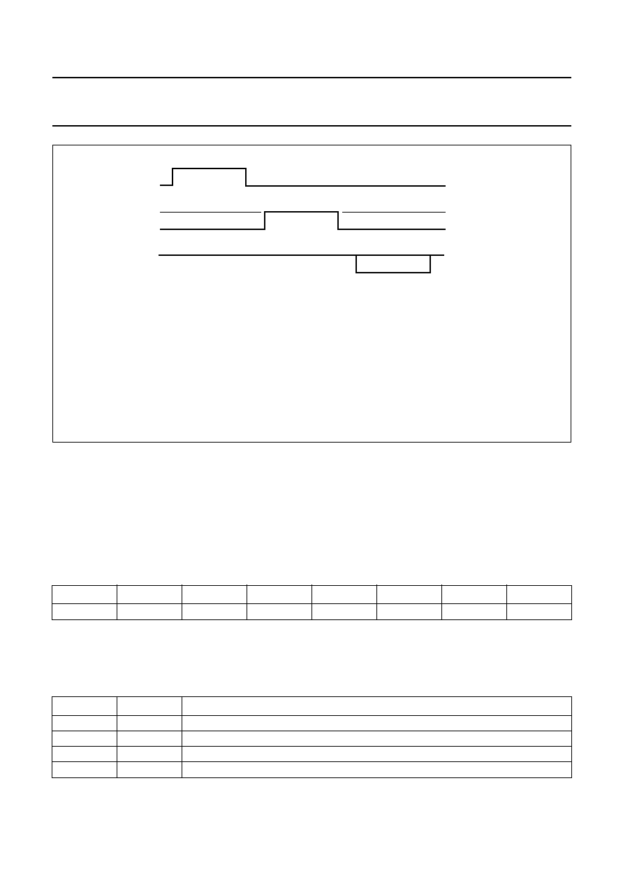
1997 Nov 17
29
Philips Semiconductors
Preliminary specification
ISO/MPEG Audio Source Decoder
SAA2502
7.6.5
T
RANSFER PROTOCOLS
7.6.5.1
L3 transfer protocol
The protocol enables writing of settings and reading of status and/or data. In this protocol, the host first issues a 6-bit
wide `device address' on CDATA while CMODE = logic 0. All devices connected to the bus read this address. Then data
transfers to or from the host are carried out while CMODE = logic 1. All devices with a different device address must
neglect these data transfers until the next address is issued. Only the device with an address equal to the issued device
address performs the transfer.
Table 20 L3 device address.
Note
1. The `Data Operation Mode' bits DOM1 and DOM0 define the current sub-mode of the control interface until the next
time a device address is issued (see Table 21).
Table 21 DOM1 and DOM0 bits
BIT 7
BIT 6
BIT 5
BIT 4
BIT 3
BIT 2
BIT 1
BIT 0
0
1
1
0
0
0
DOM1
(1)
DOM0
(1)
DOM1
DOM0
FUNCTION
0
0
data (new local register contents) sent to the SAA2502
0
1
data (current local register contents) sent to the microcontroller
1
0
local register address sent to the SAA2502
1
1
short (1 byte) SAA2502 status report sent to the microcontroller
Fig.18 Microcontroller interface initialization procedure.
(1) The value of the CMODE signal while RESET is asserted defines the microcontroller interface mode; CMODE = logic 1 = I
2
C-bus,
CMODE = logic 0 = L3. No transfers can be performed (CCLK stays HIGH).
(2) L3 mode of operation only. For a correct initialization of the interface unit, it is mandatory to make CMODE HIGH and LOW again after RESET has
been de-asserted. This must occur before any L3 transfer (even to or from other devices) is performed. As shown CCLK should stay HIGH during
this step.
(3) Now the first transfer can be performed on the microcontroller bus.
Any deviation from these steps may result in undefined behaviour of the microcontroller interface, even with the possibility of disturbing transfers
to other devices connected to the control bus.
At a hard reset, all writeable data items are forced to their default values.
handbook, full pagewidth
MGE482
RESET
CMODE
CCLK
I
2
C-bus mode
L3 mode
(1)
(2)
(3)
,,,,
,,,,
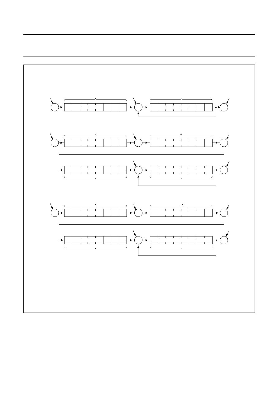
1997 Nov 17
30
Philips Semiconductors
Preliminary specification
ISO/MPEG Audio Source Decoder
SAA2502
Fig.19 L3 transfer protocol.
(1) Halt mode.
(2) Addressing mode.
(3) Data from microcontroller to SAA2502.
(4) Data from SAA2502 to microcontroller.
handbook, full pagewidth
MGE483
1
1
1
0
0
1
1
0
0
1
SAA2502 address
SAA2502 address
SAA2502 address
SAA2502 address
SAA2502 address
H
H
H
H
H
H
H
H
H
H
H
H
H
status to microcontroller
local register address
local register data to microcontroller
local register address
microcontroller data to local register
(2)
(2)
(2)
(2)
(2)
(1)
(1)
(1)
(1)
(1)
(1)
(1)
(1)
(1)
(1)
(1)
(1)
(1)
(4)
(3)
(3)
(3)
(4)
READ status
READ (block) data
WRITE (block) data

1997 Nov 17
31
Philips Semiconductors
Preliminary specification
ISO/MPEG Audio Source Decoder
SAA2502
7.6.5.2
I
2
C-bus transfer protocol (see Fig.20)
The protocol enables reading of data and writing of settings. In this protocol, the host first issues a 7-bit wide `device
address' on CDATA immediately after the generation of a START condition. All devices connected to the bus read this
address. Data transfers to or from the host are then carried out. All devices with a different device address must neglect
these data transfers until the next address is issued. Only the device with an address equal to the issued device address
performs the transfer.
Table 22 I
2
C-bus device address
Notes
1. R/W determines the direction of the subsequent data transfer(s): logic 0 = write, data is sent to the SAA2502;
logic 0 = read, data is sent to the microcontroller.
2. For further description of the acknowledge bit ACK consult the I
2
C-bus specification.
BIT 7
BIT 6
BIT 5
BIT 4
BIT 3
BIT 2
BIT 1
BIT 0
-
0
0
1
1
1
0
1
R/W
(1)
ACK
(2)
Fig.20 I
2
C-bus transfer protocol.
(1) START condition.
(2) STOP condition.
(3) Transfer from microcontroller to SAA2502.
(4) Transfer from SAA2502 to microcontroller.
handbook, full pagewidth
MGE484
0
0
1
0
0
0
SAA2502 address
SAA2502 address
SAA2502 address
P
P
S
S
S
local register address
local register data to microcontroller
local register data to microcontroller
local register address
microcontroller data to local register
(2)
(1)
(1)
(1)
(2)
(4)
(4)
(4)
(4)
(4)
(4)
(3)
(3)
(2)
(3)
(3)
(3)
(3)
(3)
(4)
(4)
READ (block) data
WRITE (block) data
0
0
1
0
0

1997 Nov 17
32
Philips Semiconductors
Preliminary specification
ISO/MPEG Audio Source Decoder
SAA2502
Data is transferred to or from the SAA2502 in local register
units (1 byte). Local registers may be of readable and/or of
writeable type. A local register transfer is initiated by
writing the corresponding local register address. The local
register unit content is then transferred.
7.6.5.3
Register block type
Some sets of local registers are organized in blocks.
One local register address is assigned to a complete block.
The local register block address points to the first local
register of the block. Blocks may be accessed only
sequentially by reading or writing successively to the
individual members of the block. Reading or writing a
restricted type block may be interrupted if desired by
stopping at any location in the block. Transferring may
then continue later via a new block operation using a
special local address (provided that no other restricted
type local SAA2502 address has been sent since). This
special address is labelled `continue block'
(see Section 7.6.6.11).
The set of four APU registers is a special type that has an
auto increment option. The local addresses of these
registers are adjacent to each other. To save time there is
an option to programme them in sequence, in one I
2
C-bus
transmission.
After an initial local address (14H to 17H) the data for each
APU coefficient follows in sequence, without the need for
transmitting other local addresses. The auto increment will
(if required) scroll round from the last local address (17H)
back to the first local address (14H).
Only the APU registers have local addresses that provide
the auto increment option.
Several individual registers store more than one byte of
data. To program them, transmit their local address,
followed by all the data bytes, in sequence.
7.6.5.4
Restricted type registers
Some local registers and/or local register blocks are of the
so-called `restricted type'. Access of such registers is
subject to the following limitations:
∑
Transfer speed in L3 mode is limited to 800 kbits/s.
There are no special speed limitations in I
2
C-bus mode
other than the 400 kbits/s specification limit. Both
maximum speeds are scaled down proportionally when
the MCLK24 frequency is below maximum.
∑
Restricted registers should not be accessed more
frequently than once per audio frame.
Section 7.6.6 describes the category of each local
register/block.
7.6.6
L
OCAL REGISTERS
7.6.6.1
Status
The host may check the SAA2502 status by reading the
one byte status word. Reading status may be
accomplished in two ways:
∑
Using the special read status protocol of the L3 mode
∑
Using the normal data exchange protocol.
The status byte read branch of the protocol may be looped
an arbitrary number of times. If read is looped, status is
updated between individual readings. The status bits are
shown in Table 23.
Table 23 Status register: status is 1 byte (read-only, unrestricted type, local address = 1AH)
BIT 7
BIT 6
BIT 5
BIT 4
BIT 3
BIT 2
BIT 1
BIT 0
DST1
DST1
undefined
undefined
undefined
undefined
INSYNC
undefined
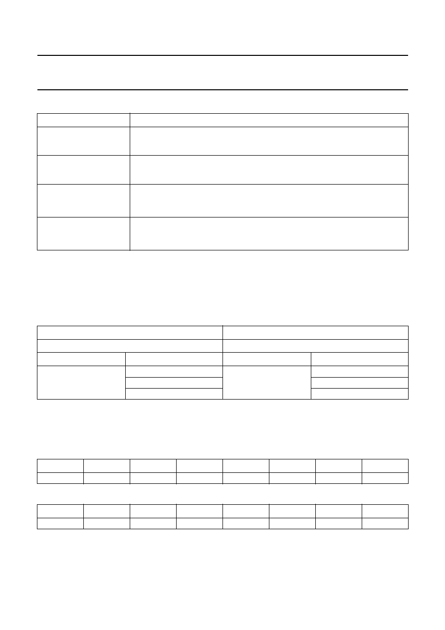
1997 Nov 17
33
Philips Semiconductors
Preliminary specification
ISO/MPEG Audio Source Decoder
SAA2502
Table 24 Explanation of bits in Table 23
Notes
1. DST0 values in general do not have a determined duration. However, DST0 = logic 1 lasts at least 0.4 frame period
when MPEG layer I data is decoded, and 0.8 frame period when MPEG layer II data is decoded. Table 25 indicates
the validity of the SAA2502 readable data items with respect to the decoding subprocess.
2. Some of the readable local register bits only have significance if INSYNC is logic 1.
Table 25 Validity of the SAA2502 readable data items with respect to the decoding subprocess
Note
1. Reading of a data item in a period when it is not valid renders undefined data
7.6.6.2
Clock generator control
Table 26 Clock generator control 1: 1 byte (write-only, unrestricted type, local address = 11H)
Table 27 Clock generator control 2: 1 byte (write-only, unrestricted type, local address = 12H)
BIT
DESCRIPTION
DST1 and DST0
By interpreting DST1 and 0, the host can synchronize to the input frame frequency and
also determine at which moment specific data items are available to be read. The value
of DST1 and 0 is only valid if flag INSYNC is set.
DST1
This is a modulo 2 frame counter, i.e. DST1 inverts at the moment the decoding of a
new frame is started. DST1 enables the host to sample the data items available flag
DST0 less frequently, meanwhile enabling the host to see if it missed a state.
DST0
Bit indicates whether data items are available to be read; note 1:
logic 0 indicates updating of data items is in progress (consequently they are invalid)
logic 1 indicates ancillary (or PAD) data, frame headers and error report are valid.
INSYNC
Synchronization indication:
logic 0 indicates not synchronized to input audio frame borders
logic 1 indicates synchronized to input audio frame borders; note 2.
DECODING FRAME n
DECODING FRAME n + 1
DST1 = 0
DST1 = 1
DST0 = 0
DST0 = 1
DST0 = 0
DST0 = 1
Not valid; note 1
ancillary data (frame n
-
1)
not valid; note 1
ancillary data (frame n)
frame headers (frame n)
frame headers (frame n + 1)
error report (frame n)
error report (frame n+1)
BIT 7
BIT 6
BIT 5
BIT 4
BIT 3
BIT 2
BIT 1
BIT 0
FSCINP
FSC384
FSCENA
N3b4
N3b3
N3b2
N3b1
N3b0
BIT 7
BIT 6
BIT 5
BIT 4
BIT 3
BIT 2
BIT 1
BIT 0
N2b1
N2b0
N1b3
N1b2
N1b1
N1b0
PHSRVS
PHSMOD

1997 Nov 17
34
Philips Semiconductors
Preliminary specification
ISO/MPEG Audio Source Decoder
SAA2502
Table 28 Explanation of bits in Tables 26 and 27
Note
1. Default settings (settings value after a hard reset).
7.6.6.3
Input and decoding control
Table 29 Input and decoding control: 1 byte (write-only, restricted type, local address = 33H)
BIT
DESCRIPTION
FSCINP
external sample clock mode:
logic 0
(1)
: internal sample clock mode (sample clock derived from MCLKIN and X22IN clock inputs)
logic 1: external sample clock mode (FSCLKIN is sample clock input)
FSC384
external sample clock frequency indication:
logic 0
(1)
: FSCLKIN is 256
◊
f
s
logic 1: FSCLKIN is 384
◊
f
s
FSCENA
FSCLK output enable flag:
logic 0
(1)
: FSCLK output is disabled
logic 1: FSCLK output is enabled
PHSMOD
phase detector mode of operation:
logic 0
(1)
: edge triggered mode of operation
logic 1: XOR mode of operation
PHSRVS
reversed phase detection:
logic 0
(1)
: normal phase detection
logic 1: reversed phase detection (characteristics mirrored with reference to vertical axis)
N1b3 to 0
code for N1 value:
`0'
(1)
N1 = 8; `1' N1 = 16; `2' N1 = 24; `3' N1 = 32; `4' N1 = 40; `5' N1 = 48; `6' N1 = 56; `7' N1 = 64
N2b1 to 0
code for N2 value:
`0'
(1)
N2 = 5; `1' N2 = 25; `2' N2 = 125; `3' N2 = 625
N3b4 to 0
N3
-
1; range 0
(1)
to 31 (N3 is 1 to 32)
BIT 7
BIT 6
BIT 5
BIT 4
BIT 3
BIT 2
BIT 1
BIT 0
SYMOD1
SYMOD0
INMOD1
INMOD0
STOPRQ
CRCACT
SELCH2
SFCRC

1997 Nov 17
35
Philips Semiconductors
Preliminary specification
ISO/MPEG Audio Source Decoder
SAA2502
Table 30 Explanation of bits in Table 29
Notes
1. Default settings (settings value after a hard reset).
2. The SAA2502 can only decode one of the dual channels, at a time. Both left and right audio outputs then play the
selected channel.
Table 31 Sampling rate and bit rate: 1 byte (write-only, unrestricted type, local address = 1BH)
Table 32 Soft reset: 1 byte (write-only, unrestricted type, local address = 1EH)
BIT
DESCRIPTION
SYMOD1 and SYMOD0
audio frame synchronization mode:
00
(1)
: general non-byte aligned frame synchronization
01: MPEG layer II non-byte aligned frame synchronization
10: byte aligned frame synchronization
11: sync pulse frame synchronization
INMOD1 and INMOD0
input interface mode of operation:
00
(1)
: master input mode for static bit rates
01: slave input mode for static bit rates
10: buffer controlled input mode for static bit rates
11: buffer controlled input mode for variable bit rates
STOPRQ
enable stop requesting flag:
0
(1)
: input requesting continues when STOP = logic 1
1: input requesting stops when STOP = logic 1
CRCACT
CRC presence:
0
(1)
: protection bit in the MPEG frame header is used to determine CRC presence
1: CRC is assumed be present by definition (the protection bit is overruled)
SELCH2
(2)
dual channel mode channel select (with other modes of input data = don't care):
0
(1)
: select channel I
1: select channel II
SFCRC
enable scale factor CRC protection:
0
(1)
: no scale factor protection
1: scale factor CRC protection enabled
BIT 7
BIT 6
BIT 5
BIT 4
BIT 3
BIT 2
BIT 1
BIT 0
SFX2
SFX1
SFX0
BRX4
BRX3
BRX2
BRX1
BRX0
BIT 7
BIT 6
BIT 5
BIT 4
BIT 3
BIT 2
BIT 1
BIT 0
0
0
0
0
0
0
0
0
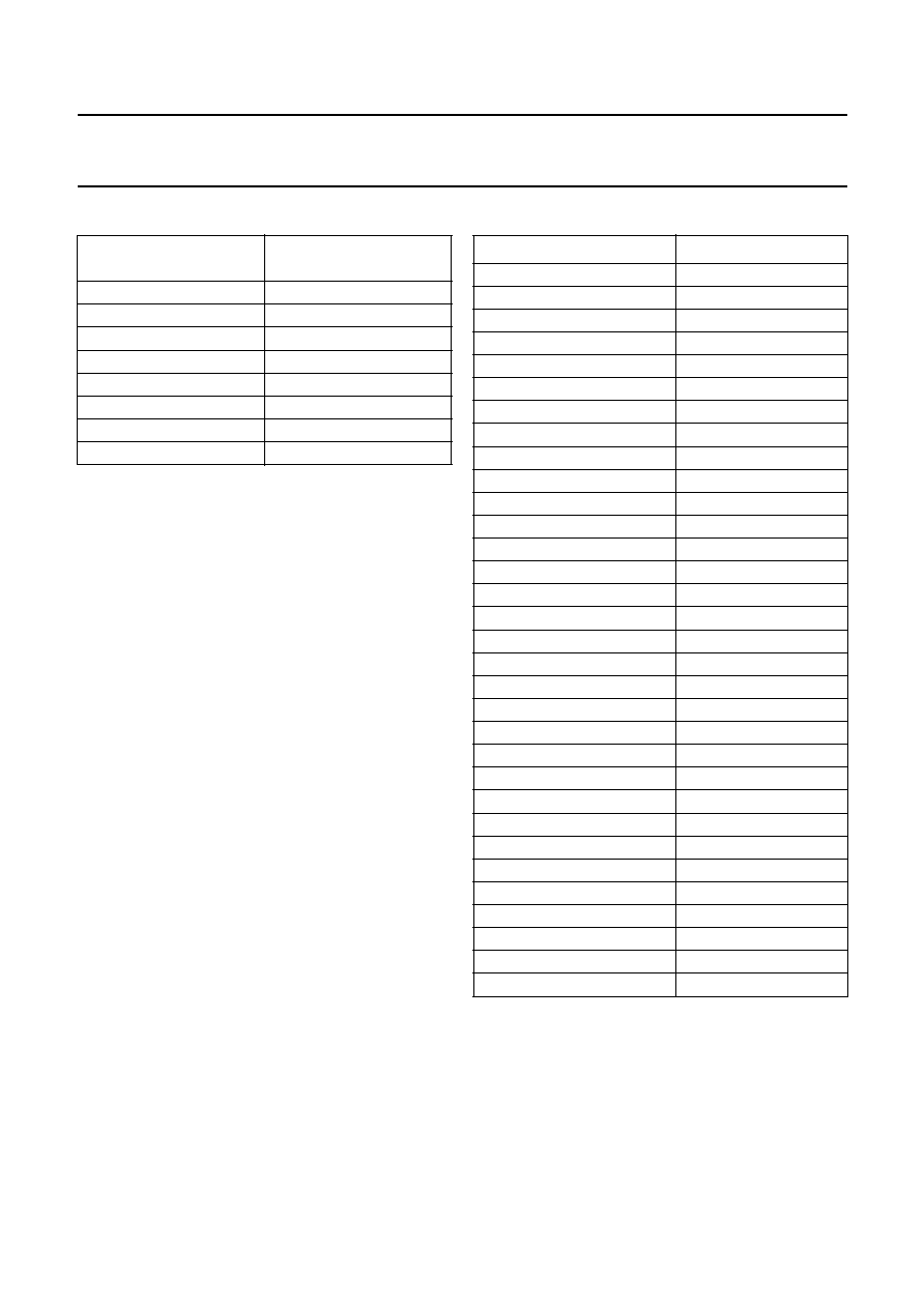
1997 Nov 17
36
Philips Semiconductors
Preliminary specification
ISO/MPEG Audio Source Decoder
SAA2502
Table 33 Sample frequency index setting
Notes
1. Modification of SFX values is only possible while
INSYNC = logic 0. Writing the sample rate control
word while INSYNC = logic 1 will have no effect.
2. Default settings (settings value after a hard reset).
SFX2 to SFX0
(1)
SAMPLE FREQUENCY
(kHz)
000
22.05
001
24
010
16
011
-
100
44.1
(2)
101
48
110
32
111
-
Table 34 Input bit rate index setting
Notes
1. Modification of BRX values is only possible while
INSYNC = logic 0. Writing the bit rate control word
while INSYNC = logic 1 will have no effect.
2. Default settings (settings value after a hard reset).
BRX4 to BRX0
(1)
BIT RATE (kbits/s)
00000
-
00001
8
00010
16
00011
24
00100
32
00101
40
00110
48
00111
56
01000
-
01001
16
01010
32
01011
48
01100
64
01101
80
01110
96
01111
112
10000
128
10001
144
10010
160
10011
176
10100
192
10101
-
10110
224
10111
-
11000
256
11001
288
11010
320
11011
352
11100
384
(2)
11101
416
11110
448
11111
-
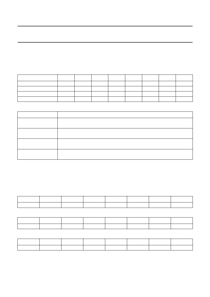
1997 Nov 17
37
Philips Semiconductors
Preliminary specification
ISO/MPEG Audio Source Decoder
SAA2502
7.6.6.4
Soft reset
Writing to this local address has the same effect as a rising edge at the STOP input (pin 12).
7.6.6.5
Dynamic range compression control
Table 35 DRC control registers: 4 bytes (read/write, restricted block type, local address = 20H)
Table 36 Explanation of bits in Table 35
Note
1. Default settings (settings value after a hard reset).
7.6.6.6
Output control
The output interface is controlled by 4 local registers and a register block.
Table 37 Output control register: 1 byte (write-only, unrestricted type, local address = 10H)
Table 38 SPDIF sf code 1: 1 byte (write-only, unrestricted type, local address = 18H)
Table 39 SPDIF sf code 2: 1 byte (write-only, unrestricted type, local address = 19H)
SUBSEQUENT BYTES
7
6
5
4
3
2
1
0
Compression slope
CSLP7
CSLP6
CSLP5
CSLP4
CSLP3
CSLP2
CSLP1
CSLP0
Maximum compression
0
CMAX6
CMAX5
CMAX4
CMAX3
CMAX2
CMAX1
CMAX0
Compression offset
COFS7
COFS6
COFS5
COFS4
COFS3
COFS2
COFS1
COFS0
Release rate
0
0
0
CRRT4
CRRT3
CRRT2
CRRT1
CRRT0
BIT
DESCRIPTION
CSLP7 to CSLP0
compression slope
range 0
(1)
to 255; unit =
1
/
256
dB per dB
CMAX6 to CMAX0
maximum amplification
range 0
(1)
to 127; unit =
3
/
16
dB
COFS7 to COFS0
compression offset
range 0
(1)
to 255; unit =
3
/
16
dB
CRRT4 to CRRT0
release rate
range 1
(1)
to 31; unit =
3
/
256
dB per 384 samples
BIT 7
BIT 6
BIT 5
BIT 4
BIT 3
BIT 2
BIT 1
BIT 0
SPDENA
I2SENA
ANAENA
ANARTZ
RND1
RND0
SPD_V
SPD_C
BIT 7
BIT 6
BIT 5
BIT 4
BIT 3
BIT 2
BIT 1
BIT 0
22C3
22C2
22C1
22C0
24C3
24C2
24C1
24C0
BIT 7
BIT 6
BIT 5
BIT 4
BIT 3
BIT 2
BIT 1
BIT 0
0
0
0
0
16C3
16C2
16C1
16C0

1997 Nov 17
38
Philips Semiconductors
Preliminary specification
ISO/MPEG Audio Source Decoder
SAA2502
Table 40 SPDIF user byte: 1 byte (write-only, unrestricted type, local address = 1FH)
Table 41 Explanation of bits in Tables 37, 38, 39 and 40
Notes
1. Default settings (settings value after a hard reset).
2. ANARTZ = logic 1 is only allowed in internal sample clock mode; FSCINP = logic 0 in clock generator control word 1.
APU coefficients are set by writing their 8-bit indices to the 4-byte APU coefficient local register block. At a hard reset,
indices LL and RR are set to 0 (no attenuation) and indices LR and RL to 255 (infinite attenuation; no crosstalk).
BIT 7
BIT 6
BIT 5
BIT 4
BIT 3
BIT 2
BIT 1
BIT 0
SPDU7
SPDU7
SPDU5
SPDU4
SPDU3
SPDU2
SPDU1
SPDU0
BIT
DESCRIPTION
SPDENA
enable SPDIF output pin:
logic 0
(1)
: SPDIF output pin is disabled
logic 1: SPDIF output pin is enabled
I2SENA
enable I
2
S output:
logic 0
(1)
: I
2
S output is disabled
logic 1: I
2
S output is enabled
ANAENA
enable analog output:
logic 0: analog output is disabled
logic 1
(1)
: analog output is enabled
ANARTZ
analog output return-to-zero mode:
logic 0
(1)
: non return-to-zero mode; subsequent logic 1's in analog outputs are merged
logic 1
(2)
: return-to-zero mode; subsequent logic 1's in analog outputs are separated
RND1 and 0
I
2
S and SPDIF output sample rounding control:
00
(1)
: output rounded to 16 bits
01: output rounded to 18 bits
10: output rounded to 20 bits
11: output rounded to 22 bits
SPD_V
value of validity flag (V bit) in SPDIF output format:
logic 0
(1)
: valid
logic 1: not valid
SPD_C
value of copy permission flag (C bit) in SPDIF output format:
logic 0
(1)
: copy prohibited
logic 1: copy permitted
22C3 to 22C0
SPDIF code used for 22.05 kHz sample frequency; default = 0100
(1)
24C3 to 24C0
SPDIF code used for 24 kHz sample frequency; default = 0110
(1)
16C3 to 16C0
SPDIF code used for 16 kHz sample frequency; default = 0111
(1)
SPDU7 to SPDU0
SPDIF user byte (content of byte is sent on SPDIF user channel); default = inactive
(1)
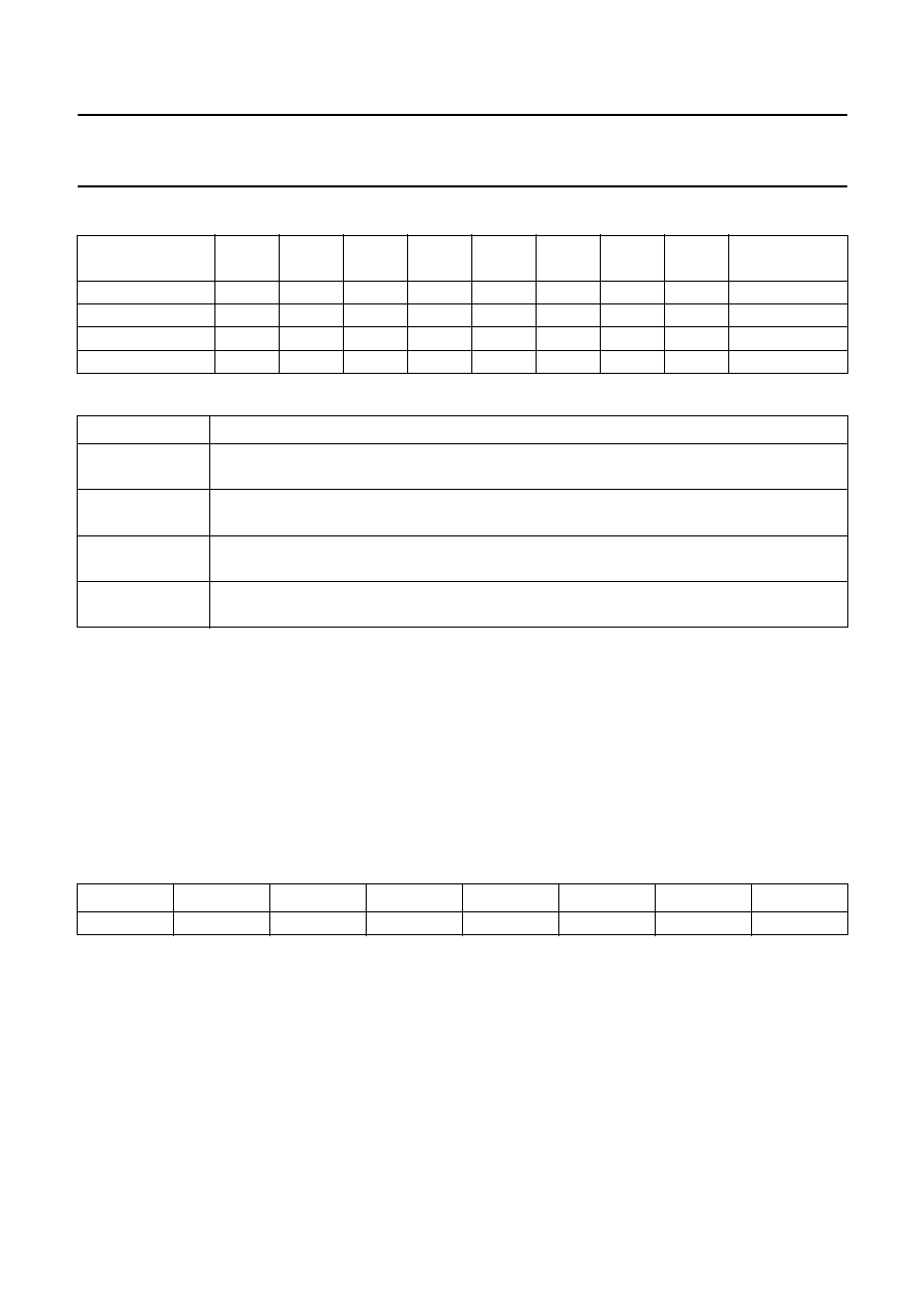
1997 Nov 17
39
Philips Semiconductors
Preliminary specification
ISO/MPEG Audio Source Decoder
SAA2502
Table 42 APU coefficients: 4 bytes (read/write, unrestricted special block type
Table 43 Explanation of bits in Table 42
Note
1. Default settings (settings value after a hard reset).
The APU coefficient block type is a special one:
∑
Block accesses may start at any individual coefficient (each has its own local address)
∑
Block accesses may also extent past RR (the block access will wrap around to LL).
7.6.6.7
Interrupt control
Interrupt generation is controlled using two separate single byte local registers.
Table 44 Interrupt event register: 1 byte (read-only, unrestricted type, local address = 1CH)
The separate bits of the interrupt event register indicate the occurrence of the events shown in Table 44
SUBSEQUENT
BYTES
BIT 7
BIT 6
BIT 5
BIT 4
BIT 3
BIT 2
BIT 1
BIT 0
LOCAL
ADDRESS
APU coefficient LL
LL7
LL6
LL5
LL4
LL3
LL2
LL1
LL0
14H
APU coefficient LR
LR7
LR6
LR5
LR4
LR3
LR2
LR1
LR0
15H
APU coefficient RL
RL7
RL6
RL5
RL4
RL3
RL2
RL1
RL0
16H
APU coefficient RR
RR7
RR6
RR5
RR4
RR3
RR2
RR1
RR0
17H
BIT
DESCRIPTION
LL7 to LL0
left channel in to left channel out attenuation index
range 0
(1)
to 255; see Fig.14
LR7 to LR0
left channel in to right channel out attenuation index
range 0 to 255
(1)
; see Fig.14
RL7 to RL0
right channel in to left channel out attenuation index
range 0 to 255
(1)
; see Fig.14
RR7 to RR0
right channel in to right channel out attenuation index
range 0
(1)
to 255; see Fig.14
BIT 7
BIT 6
BIT 5
BIT 4
BIT 3
BIT 2
BIT 1
BIT 0
undefined
undefined
undefined
DST0U
STOP
CRCERR
INSNC
NOSNC
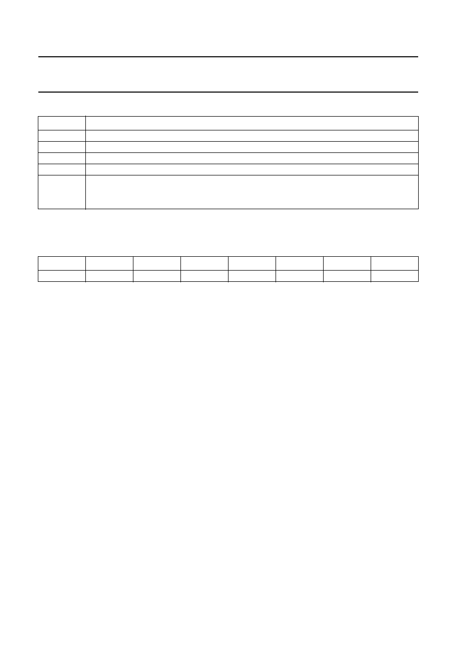
1997 Nov 17
40
Philips Semiconductors
Preliminary specification
ISO/MPEG Audio Source Decoder
SAA2502
Table 45 Explanation of bits in Table 44
Note
1. Default settings (settings value after a hard reset).
Table 46 Interrupt masking register: 1 byte (write-only, unrestricted type, local address = 1DH)
The individual bits of the interrupt masking register (Table 46) may mask the interrupt events at the same bit location in
the interrupt event register (Table 44):
logic 0 (default setting, setting value after a hard reset); interrupt event is masked.
logic 1; interrupt event is not masked.
Masked interrupt are still flagged in the interrupt event register, they just do NOT have an effect on the INTRPT interrupt
pin (thus polling of masked interrupts is possible).
BIT
DESCRIPTION
DST0U
DST0 has been set (valid ancillary/PAD data, headers and error report)
STOP
rising edge of STOP input signal
CRCERR
MPEG CRC check failed
INSNC
status bit INSYNC was set
NOSNC
status bit INSYNC was cleared
logic 0
(1)
; no interrupt for this event
logic 1; interrupt for this event
BIT 7
BIT 6
BIT 5
BIT 4
BIT 3
BIT 2
BIT 1
BIT 0
0
0
0
IMSK4
IMSK3
IMSK2
IMSK1
IMSK0

1997 Nov 17
41
Philips Semiconductors
Preliminary specification
ISO/MPEG Audio Source Decoder
SAA2502
7.6.6.8
Frame headers
Information about input data, derived by the SAA2502 from the input data frame headers, may be read from the frame
header items. Both the frame header bytes decoded from the input bit stream and the header bytes used for the actual
decoding may be read.
The decoded frame header item is valid independent of the value of status flag INSYNC. It shows, for example, the
decoded headers while the SAA2500 is in the process of synchronizing.
The used frame header item is only valid if status flag INSYNC is set. The used header bytes are derived by the SAA2502
from the decoded header bytes by filling in known header fields (e.g. those that have a fixed value) and overruling
detected errors.
Table 47 Decoded frame header: 3 bytes (read-only, restricted block type, local address = 21H)
Note
1. The EMPH1 and EMPH0 bits may only be used to monitor the current de-emphasis indication. Corresponding
de-emphasis is performed automatically before outputting the baseband audio signal.
Table 48 Used frame header: 3 bytes (read-only, restricted block type, local address = 22H)
Note
1. The EMPH1 and EMPH0 bits may only be used to monitor the current de-emphasis indication. Corresponding
de-emphasis is performed automatically before outputting the baseband audio signal.
Table 49 Explanation of bits in Tables 47 and 48
SUBSEQUENT BYTES
BIT 7
BIT 6
BIT 5
BIT 4
BIT 3
BIT 2
BIT 1
BIT 0
Decoded header byte 1
SY3
SY2
SY1
SY0
ID
LAY1
LAY0
NOPR
Decoded header byte 2
BR3
BR2
BR1
BR0
FS1
FS0
undefined undefined
Decoded header byte 3
MOD1
MOD0
MODX1
MODX0
COPR
ORIG
EMPH1
(1)
EMPH0
(1)
SUBSEQUENT BYTES
BIT 7
BIT 6
BIT 5
BIT 4
BIT 3
BIT 2
BIT 1
BIT 0
Used header byte 1
1
1
1
1
ID
1
LAY0
NOPR
Used header byte 2
BR3
BR2
BR1
BR0
FS1
FS0
undefined undefined
Used header byte 3
MOD1
MOD0
MODX1
MODX0
COPR
ORIG
EMPH1
(1)
EMPH0
(1)
BIT
DESCRIPTION
SY3 to SY0
last 4 bits of the synchronization word
ID
algorithm identification
LAY1 and LAY0
layer
NOPR
flag for CRC on header plus bit allocation plus scale factor select information
BR3 to BR0
bit rate index
FS1 and FS0
sample rate index
MOD1 and MOD0
mode
MODX1 and MODX0
mode extension
COPR
copyright flag
ORIG
original or home copy flag
EMPH1 and EMPH0
audio de-emphasis indication

1997 Nov 17
42
Philips Semiconductors
Preliminary specification
ISO/MPEG Audio Source Decoder
SAA2502
7.6.6.9
Error report
The validity of bit allocation plus scale factor select information and the result of the scale factor CRCs (only when scale
factor CRCs are enabled) may be read from the error report register. The error report is only valid when status flag
INSYNC is set.
Table 50 Error report register: 1 byte (read-only, restricted type, local address = 24H)
Table 51 Explanation of bits in Table 50
BIT 7
BIT 6
BIT 5
BIT 4
BIT 3
BIT 2
BIT 1
BIT 0
BALOK
DECFM
undefined
undefined
SF3OK
SF2OK
SF1OK
SF0OK
BIT
DESCRIPTION
BALOK
bit allocation and scale factor select information validity indication:
logic 0; bit allocation or scale factor select information are incorrect or the CRC over
header plus bit allocation plus scale factor select information has failed
logic 1; bit allocation and scale factor select information are correct and CRC over
header plus bit allocation plus scale factor select information is correct or not active
DECFM
frame skipping or frame decoding indication:
logic 0; current input data frame is skipped, and the corresponding baseband audio
output frame is muted due to input data errors or inconsistencies; audio frame
synchronization is maintained
logic 1; current frame is decoded normally
SF3OK to SF0OK
scale factor CRCs not enabled; bits are invalid
scale factor CRCs enabled:
logic 0; one or more scale factors have been concealed in sub-band block 0 to 3
logic 1; no scale factor concealment in sub-band block 0 to 3 (CRC check was OK)
block 0; sub-bands 0 to 3
block 1; sub-bands 4 to 7
block 2; sub-bands 8 to 15
block 3; sub-bands 16 to 31

1997 Nov 17
43
Philips Semiconductors
Preliminary specification
ISO/MPEG Audio Source Decoder
SAA2502
7.6.6.10
Ancillary data and program associated data
With standard MPEG input data, the last 54 bytes of each frame, which may carry Ancillary Data (AD), are buffered by
the SAA2502 to be read by the host. Subsequent ancillary data bytes are read in reversed order with respect to their
order in the input data bit stream; the first item data byte is the last frame byte in the input bit stream. The ancillary data
block of local registers is refilled for every frame. The host must either know or determine itself how many of the ancillary
data bytes are valid per frame. The ancillary data block contains only valid data when status flag INSYNC is set.
Table 52 Ancillary data: 54 bytes (read-only, restricted block type, local address = 25H)
Similarly when scale factor CRCs are enabled, the Fixed Program Associated Data (FPAD) and extended Program
Associated Data (XPAD) bytes contained in each frame may be read, with the 2 FPAD bytes first, followed by maximum
52 XPAD bytes. Subsequent FPAD and XPAD bytes are read in reversed order with respect to their order in the input
data bit stream; the first item data byte is the last PAD byte in the input bit stream. The host must determine itself how
many of the XPAD bytes are valid per frame by interpretation of the FPAD content. The PAD data block contains only
valid data when status flag INSYNC is set.
Table 53 XPAD plus FPAD: 54 bytes (read-only, restricted block type, local address = 25H)
7.6.6.11
Continue block operation
Local address 00H is reserved for continuation of restricted type block operations. Whenever this local address is used,
it will result in continuation of any restricted type block transfer at the point where it was interrupted (provided that no
other restricted type SAA2502 transfer was carried out since).
SUBSEQUENT BYTES
7
6
5
4
3
2
1
0
AD byte 1 to byte 54
bit 7
bit 6
bit 5
bit 4
bit 3
bit 2
bit 1
bit 0
SUBSEQUENT BYTES
7
6
5
4
3
2
1
0
FPAD bytes 1 and 2;
XPAD byte 1 to byte 52
bit 7
bit 6
bit 5
bit 4
bit 3
bit 2
bit 1
bit 0

1997 Nov 17
44
Philips Semiconductors
Preliminary specification
ISO/MPEG Audio Source Decoder
SAA2502
8
APPENDIX
8.1
L3 interface specification
8.1.1
I
NTRODUCTION
The main purpose of the interface definition is to define a
protocol that allows for the transfer of control information
and operational details between a microcontroller and a
number of slave devices, at a rate that exceeds other
common interfaces, but with a sufficient low complexity for
application in consumer products. It should be clearly
noted that the current interface definition is intended for
use in a single apparatus, preferably restricted to a single
printed circuit board.
The interface requires 3 signal lines (apart from a return
`ground') between the microcontroller and the slave
devices (from this the name `L3' is derived). These 3-lines
are common to all ICs connected to the bus:
1. L3MODE
2. L3DATA
3. L3CLK.
L3MODE and L3CLK are always driven by the
microcontroller, L3DATA is bidirectional:
Table 54 The 3-lines common to all ICs; L3MODE,
L3CLK and L3DATA
Notes
1. L3MODE is used for the identification of the operation
mode.
2. L3CLK is the bit clock to which the information transfer
will be synchronized.
3. L3DATA will carry the information to be transferred.
SIGNAL
MICROCONTROLLER
SLAVE
DEVICE
L3MODE
(1)
output
input
L3CLK
(2)
output
input
L3DATA
(3)
output/input
input/output
All slave devices in the system can be addressed using a
6 bit address. This allows for up to 63 different slave
devices, as the all `0' address is reserved for special
purposes.
In operation 2 modes can be identified:
1. Addressing Mode (AM).
During addressing mode a single byte is sent by the
microcontroller. This byte consists of 2 Data Operation
Mode (DOM) bits and 6 Operational Address (OA)
bits. Each of the slave devices evaluates the
operational address. Only the device that has been
issued the same operational address will become
active during the following data mode. The operation
to be executed during the data mode is indicated by
the two data operation mode bits.
2. Data Mode (DM).
During data mode information is transferred between
microcontroller and slave device. The transfer
direction may be from microcontroller to slave (`write')
or from slave to microcontroller (`read'). However,
during one data mode the transfer direction can not
change.
8.1.1.1
Addressing mode
In order to start an addressing mode the microcontroller
will make the L3MODE line LOW. The L3CLK line is
lowered 8 times during which the L3DATA line transfers
8 bits. The information is presented LSB first and remains
stable during the LOW phase of the L3CLK signal.
The addressing mode is ended by making the L3MODE
line HIGH.
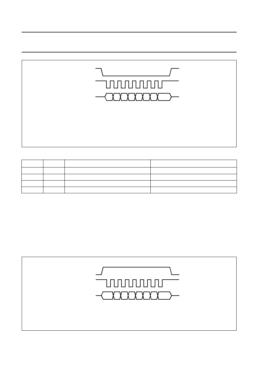
1997 Nov 17
45
Philips Semiconductors
Preliminary specification
ISO/MPEG Audio Source Decoder
SAA2502
Table 55 Preferred allocations
DOM1
DOM0
FUNCTION
REMARKS
0
0
data from microcontroller to SAA2500
general purpose data transfer
0
1
data from SAA2500 to microcontroller
general purpose data transfer
1
0
control from microcontroller to SAA2500
register selection for data transfer
1
1
status from SAA2500 to microcontroller
short device status message
handbook, halfpage
0
1
2
3
4
5
6
7
L3MODE
L3CLK
L3DATA
MGB505
Fig.21 Addressing mode.
The meaning of the bits on L3DATA.
Bit 0 and bit 1; these are the Data Operation Mode (DOM) bits that indicate the nature of the following data transfer. The preferred allocations are
given in Table 55.
Bit 2 to bit 7; these bits act as 6 bit operational IC address, with bit 7 as MSB and bit 2 as LSB.
8.1.1.2
Data mode
In the data mode the microcontroller sends or receives
information to or from the selected device. During data
transfer the L3MODE line is HIGH. The L3CLK line is
lowered 8 times during which the L3DATA line carries
8 bits. The information is presented LSB first and remains
stable during the LOW phase of the L3CLK signal.
The basic data transfer unit is an 8-bit byte. No other basic
data transfer unit is allowed.
8.1.1.3
Halt mode
In between transfer units the L3MODE line will be driven
LOW by the microcontroller to indicate the completion of a
unit transfer. This is called `Halt Mode' (HM). During halt
mode the L3CLK line remains HIGH (to distinguish it from
an addressing mode).
handbook, halfpage
0
1
2
3
4
5
6
7
L3MODE
L3CLK
L3DATA
MGB504
Fig.22 Data transfer mode.
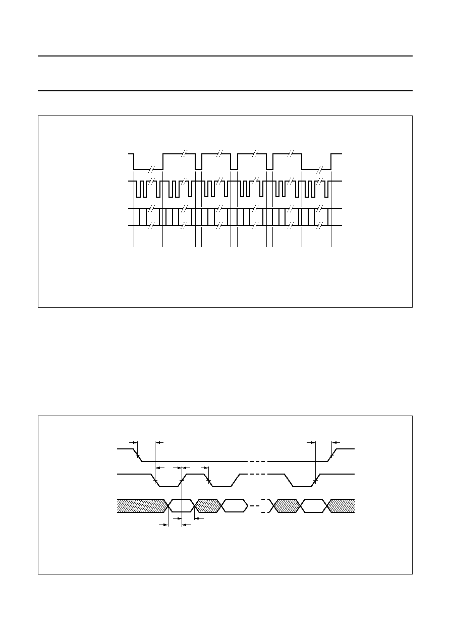
1997 Nov 17
46
Philips Semiconductors
Preliminary specification
ISO/MPEG Audio Source Decoder
SAA2502
8.1.2
E
XAMPLE OF A DATA TRANSFER
Fig.23 Example of transfer of 4 bytes.
handbook, full pagewidth
MGE485
L3 MODE
L3CLK
L3DATA
address
data
byte1
data
byte2
data
byte3
data
byte4
address
A data transfer starts when the microcontroller sends an
address on the bus. All ICs will evaluate this address, but
only the IC addressed will be an active partner for the
microcontroller in the following data transfer mode.
During the data transfer mode bytes will be sent from or to
the microcontroller. The L3MODE line is made LOW (`halt
mode') in between byte transfers. Only bytes should be
used as basic data transfer units.
After the data transfer the microcontroller does not need to
send a new address until a new data transfer is necessary.
8.1.3
T
IMING REQUIREMENTS
These are requirements for the slave devices designed in
accordance with the `L3' interface definitions.
8.1.3.1
Addressing mode
Fig.24 Timing (addressing mode).
handbook, full pagewidth
MGB507
t d1
h2
cL
t
cH
t
h1
t
su
t
t
L3CLK
L3MODE
L3DATA
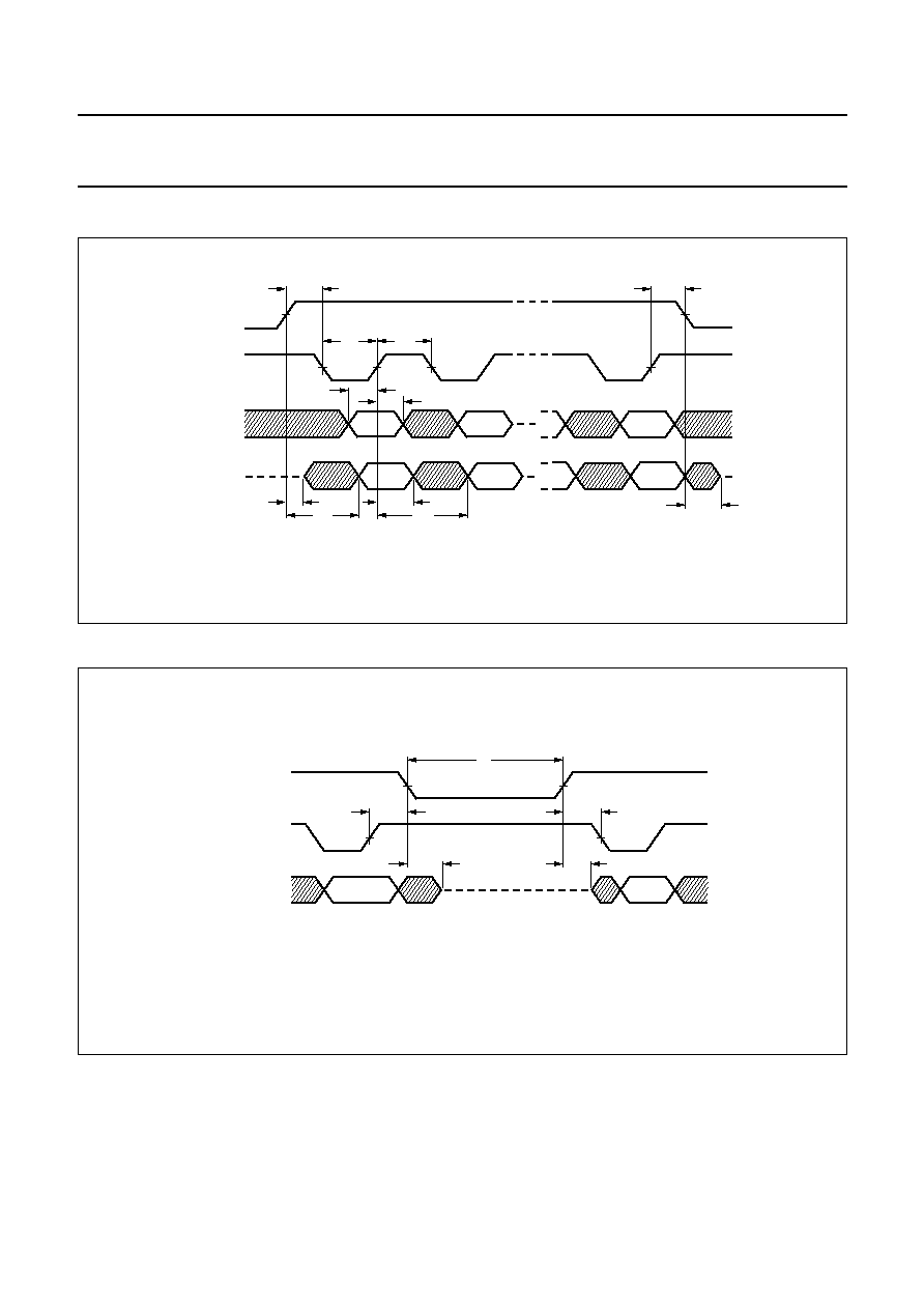
1997 Nov 17
47
Philips Semiconductors
Preliminary specification
ISO/MPEG Audio Source Decoder
SAA2502
8.1.3.2
Data transfer
8.1.3.3
Halt mode
Fig.25 Timing (data transfer).
andbook, full pagewidth
MGB508
L3DATA
microcontroller
to IC
t d1
h2
cL
t
cH
t
h1
t
su
t
t
d2
t
d3
t
h3
t
d4
t
d5
t
L3DATA
IC to
microcontroller
L3CLK
L3MODE
Fig.26 Timing (halt mode).
handbook, full pagewidth
MGB509
t
L
L3CLK
L3MODE
d5
t
h2
t
td1
d2
t
L3DATA
IC to
microcontroller
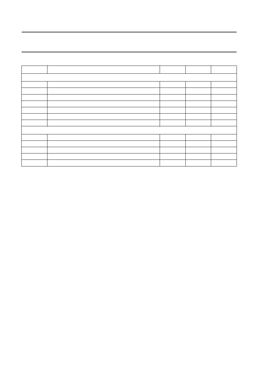
1997 Nov 17
48
Philips Semiconductors
Preliminary specification
ISO/MPEG Audio Source Decoder
SAA2502
Table 56 Requirements for timing; note 1
Notes
1. L3DATA output timing is given with 0 pF external load (derating of maximum delay = 0.5 ns/pF). Maximum external
L3DATA load = 50 pF.
2. T = 4
◊
MCLKIN cycle time if MCLK24 = logic 1; T = 2
◊
MCLKIN cycle time if MCLK24 = logic 0.
8.1.4
T
IMING
8.1.4.1
General ancillary data
If the last part of an audio frame is not occupied by encoded sub-band samples, it may be used to transfer any other data.
Definition of size, format and meaning of this so called ancillary data is completely up to the application (there are no
MPEG requirements). Non-byte aligned layer I coded input audio frames should however preferably not (always) end
with a logic 1 valued bit. In practice there are two common ways to define the size of ancillary data:
∑
The number of ancillary data bytes per frame is fixed and known by the application.
∑
There is a fixed minimum size of the ancillary data block (usually this size is small; one or two bytes). The fixed part of
the block then contains an indication of the actual size of the ancillary data block.
If room for ancillary data is present the content will be stored to be read by the microcontroller (up to a maximum of
54 bytes).
SYMBOL
PARAMETER
MIN.
MAX.
UNIT
Microcontroller to slave device; note 2
t
cL
L3CLK LOW time
T + 10
-
ns
t
cH
L3CLK HIGH time
T + 10
-
ns
t
d1
L3MODE set-up time before first L3CLK LOW
10
-
ns
t
h1
L3DATA hold time after L3CLK HIGH
10
-
ns
t
h2
L3MODE hold time after last L3CLK HIGH
15
-
ns
t
su
L3DATA set-up time before L3CLK HIGH
T + 10
-
ns
t
L
L3MODE LOW time
T + 10
-
ns
Slave device to microcontroller; note 2
t
d2
L3MODE HIGH to L3DATA enabled time
0
20
ns
t
d3
L3MODE HIGH to L3DATA stable time
-
20
ns
t
d4
L3CLK HIGH to L3DATA stable time
-
2T + 30
ns
t
d5
L3MODE LOW to L3DATA disabled time
0
20
ns
t
h3
L3DATA hold time after L3CLK HIGH
T
-
ns
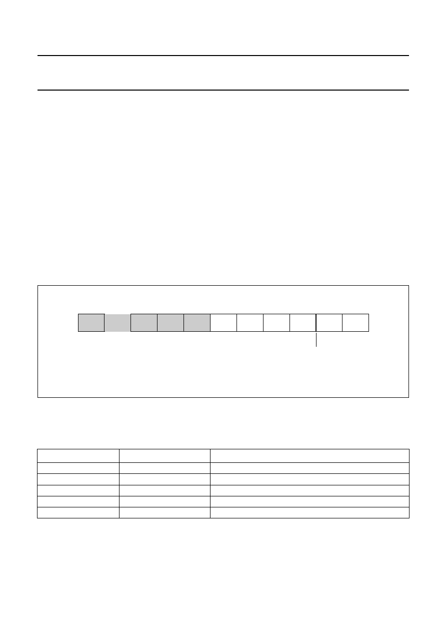
1997 Nov 17
49
Philips Semiconductors
Preliminary specification
ISO/MPEG Audio Source Decoder
SAA2502
8.1.4.2
Ancillary data containing scale factor CRCs
If scale factor CRC protection is enabled, the required CRC values for each audio frame are carried among the ancillary
data of the previous frame. This approach ensures MPEG compatibility for encoded streams with scale factor protection.
The SAA2502 assumes the next ancillary data format when scale factor CRC protection is enabled:
∑
The last 2 bytes of each audio frame carry the minimum ancillary data. These two bytes are called FPAD (fixed
program associated data) bytes. Definition of the content of FPAD is up to the application but should contain
information on the length of the remainder of the ancillary data if that length is variable. FPAD bytes are stored to be
read by the microcontroller.
∑
The byte before the FPAD bytes is called CRC0 and contains the scale factor CRC for sub-bands 0 to 3.
∑
The byte before CRC0 is called CRC1 and contains the scale factor CRC for sub-bands 4 to 7.
∑
An optional byte CRC2 may precede CRC1. It contains the scale factor CRC for sub-bands 8 to 15 and is present only
for sub-band limits greater than 8.
∑
There may be an optional byte CRC3 before CRC2. It contains the scale factor CRC for sub-bands 16 to 31 and will
be present only for sub-band limits greater than 16.
∑
Before the sub-band CRCs more ancillary data may be present. This extra ancillary data is called XPAD (extended
program associated data). If XPAD is present it will be stored to be read by the microcontroller (up to a maximum of
52 bytes).
8.1.4.3
Boundary scan test provision
The SAA2502 contains a 5-pin interface for Boundary Scan Test (BST):
Table 57 Boundary scan test
In normal use TRST must be LOW, TCK must be LOW or HIGH while TDI and TMS must be HIGH or not connected.
Otherwise when any of these pins is used in a way not designed correctly for boundary scan test purposes in the
application, damaging of the SAA2502 and/or the components surrounding it may occur.
SIGNAL
DIRECTION
FUNCTION
TDI
input
boundary scan test data input
TDO
output
boundary scan test data output
TMS
input
boundary scan test mode select
TCK
input
boundary scan test clock
TRST
input
boundary scan test reset
Fig.27 Ancillary data containing scale factor CRCs.
handbook, full pagewidth
MGE486
XPAD
52
FPAD
2
FPAD
1
XPAD
1
CRC
3
CRC
2
CRC
1
CRC
0
- - -
optional
optional
optional
optional
optional
end of frame n
start of frame n
+
1
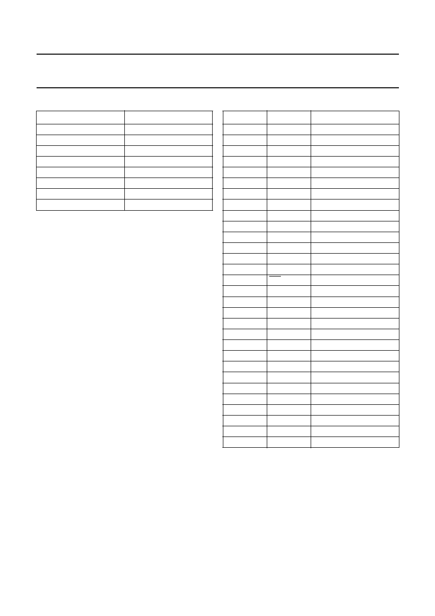
1997 Nov 17
50
Philips Semiconductors
Preliminary specification
ISO/MPEG Audio Source Decoder
SAA2502
Table 58 Boundary scan controller instructions
OPCODE
INSTRUCTION
Binary 000
ExTest
Binary 001
IDcode
Binary 010
sample
Binary 011
clamp
Binary 100
InTest
Binary 101
STCtest
Binary 110
undefined
Binary 111
bypass
Table 59 Boundary scan register definition
Notes
1. LOW or HIGH control of 2 state output.
2. LOW or HIGH control of 3 state output.
3. LOW or HIGH impedance control of 3 state output.
4. LOW or HIGH impedance control of open drain output.
NUMBER
PORT
FUNCTION
1
FSCLK
output 2; note 1
2
SCK
output 2; note 1
3
SD
output 2; note 1
4
WS
output 2; note 1
5
SPDIF
output 2; note 1
6
TC0
input
7
TC1
input
8
FSCLKIN
input
9
REFCLK
input
10
X22IN
input
11
MCLK24
input
12
MCLKIN
input
13
PHDIF
output 3; note 2
14
PHDIF
control; note 3
15
INT
open drain; note 4
16
RESET
input
17
STOP
input
18
CDRQ
output 2; note 1
19
CDEF
input
20
CDCL
input
21
CDCL
output 3; note 2
22
CDCL
control; note 3
23
CD
input
24
CDSY
input
25
CDVAL
input
26
CCLK
input
27
CDATA
input
28
CDATA
open drain; note 4
29
CDATA
control; note 3
30
CMODE
input
1997 Nov 17
51
Philips Semiconductors
Preliminary specification
ISO/MPEG Audio Source Decoder
SAA2502
8.1.4.4
Factory test scan chain provision
Table 60 Signals provided for factory test scan chain control
In normal use factory test scan chain control pins must be not connected or kept LOW. If any of these pins are pulled
HIGH in the application, damage to the SAA2502 and/or the surrounding components may occur.
8.1.4.5
Provision to read internal status
The following internal status information is made available for reading. It provides designers additional information on
status and/or progress of internal processes. This information has no meaning for the application.
Table 61 Transcoder program counter register: 1 byte (read-only, unrestricted type, local address = 10H)
Table 62 Decoder program counter register: 1 byte (read-only, unrestricted type, local address = 11H)
Table 63 Transcoder flag register: 1 byte (read-only, unrestricted type, local address = 12H)
Table 64 Transcoder and decoder branch conditions register: 1 byte (read-only, unrestricted type, local address = 13H)
SIGNAL
DIRECTION
FUNCTION
TC0
input
factory test scan chain control 0
TC1
input
factory test scan chain control 1
BIT 7
BIT 6
BIT 5
BIT 4
BIT 3
BIT 2
BIT 1
BIT 0
tPC11
tPC9
tPC8
tPC7
tPC6
tPC5
tPC4
tPC3
BIT 7
BIT 6
BIT 5
BIT 4
BIT 3
BIT 2
BIT 1
BIT 0
tPC7
tPC6
tPC5
tPC4
tPC3
tPC2
tPC1
tPC0
BIT 7
BIT 6
BIT 5
BIT 4
BIT 3
BIT 2
BIT 1
BIT 0
Undefined
tNSYNC
tORENB
tIRENB
tCRC16
tCRCF
tERRF
tSKF
BIT 7
BIT 6
BIT 5
BIT 4
BIT 3
BIT 2
BIT 1
BIT 0
dOFUL
dIRDY
dOREQ
tIEMT
tOREQ
tUPREQ
tIREQ
tPOR
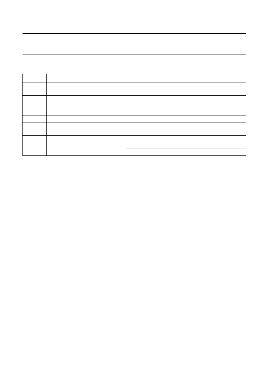
1997 Nov 17
52
Philips Semiconductors
Preliminary specification
ISO/MPEG Audio Source Decoder
SAA2502
9
LIMITING VALUES
In accordance with the Absolute Maximum Rating System (IEC 134).
Notes
1. Input voltage should not exceed 6.5 V unless otherwise specified.
2. Equivalent to discharging a 100 pF capacitor through a 1.5 k
series resistor.
3. Equivalent to discharging a 200 pF capacitor through a 0
series resistor.
SYMBOL
PARAMETER
CONDITIONS
MIN.
MAX.
UNIT
V
DD
supply voltage
-
0.5
+6.5
V
V
i
input voltage
note 1
-
0.5
V
DD
+ 0.5
V
I
DD
supply current
-
100
mA
I
SS
supply current
-
100
mA
I
I
input current
-
10
+10
mA
I
O
output current
-
20
+20
mA
P
tot
total power dissipation
-
163
mW
T
stg
storage temperature
-
65
+150
∞
C
T
amb
operating ambient temperature
-
40
+85
∞
C
V
es
electrostatic handling
note 2
-
2000
+2000
V
note 3
-
200
+200
V
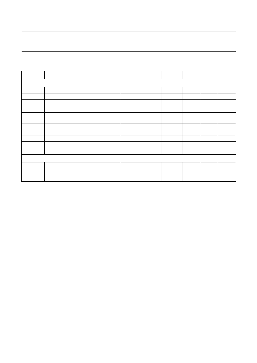
1997 Nov 17
53
Philips Semiconductors
Preliminary specification
ISO/MPEG Audio Source Decoder
SAA2502
10 DC CHARACTERISTICS
V
DD
= 4.5 to 5.5 V; T
amb
=
-
40 to +85
∞
C; unless otherwise specified.
Notes
1. Only applies to pin 25 (FSCLKIN).
2. Boundary scan test inputs.
3. All inputs except for TC0, TC1, FSCLKIN, MCLKIN, X22IN, REFP and REFN.
4. DAC outputs I
OH
= 2 mA. Typical DAC output impedance = 125
.
SYMBOL
PARAMETER
CONDITIONS
MIN.
TYP.
MAX.
UNIT
Inputs
V
IH
HIGH level input voltage (CMOS)
note 1
0.7V
DD
-
-
V
V
IL
LOW level input voltage (CMOS)
note 1
-
-
0.3V
DD
V
V
IH
HIGH level input voltage (TTL)
note 2
2
-
-
V
V
IL
LOW level input voltage (TTL)
note 2
-
-
0.8
V
V
tLH
rising edge threshold voltage
(CMOS hysteresis)
note 3
-
-
0.8V
DD
V
V
tHL
falling edge threshold voltage
(CMOS hysteresis)
note 3
0.2V
DD
-
-
V
V
hys
hysteresis voltage (CMOS hysteresis)
-
0.3V
DD
-
V
I
I
input current (all input types)
-
5
-
+5
µ
A
R
pull
pull-up or pull-down resistance
14
-
140
k
Outputs
V
OH
HIGH level output voltage
note 4
V
DD
-
0.5
-
-
V
V
OL
LOW level output voltage
note 4
-
-
0.5
V
I
LO
leakage current of a disabled output
-
-
5
µ
A
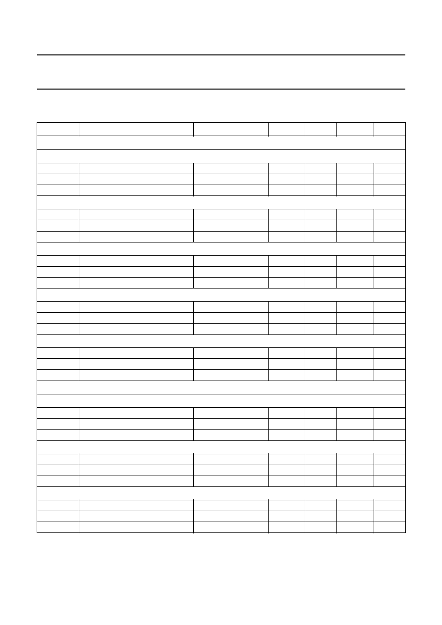
1997 Nov 17
54
Philips Semiconductors
Preliminary specification
ISO/MPEG Audio Source Decoder
SAA2502
11 AC CHARACTERISTICS
V
DD
= 4.5 to 5.5 V; T
amb
=
-
40 to +85
∞
C; unless otherwise specified.
SYMBOL
PARAMETER
CONDITIONS
MIN.
TYP.
MAX.
UNIT
Clock inputs
MCLKIN
T
cy
cycle time
40
-
-
ns
t
H
HIGH time
12
-
-
ns
t
L
LOW time
12
-
-
ns
X22IN
T
cy
cycle time
44
-
-
ns
t
H
HIGH time
12
-
-
ns
t
L
LOW time
12
-
-
ns
FSCLKIN
T
cy
cycle time
54
-
-
ns
t
H
HIGH time
12
-
-
ns
t
L
LOW time
12
-
-
ns
REFCLK
T
cy
cycle time
33
-
-
ns
t
H
HIGH time
12
-
-
ns
t
L
LOW time
12
-
-
ns
CDCL
T
cy
cycle time
note 1
8
◊
T
-
-
ns
t
H
HIGH time
note 1
T + 10
-
-
ns
t
L
LOW time
note 1
T + 10
-
-
ns
Clock outputs
FSCLK
T
cy
cycle time
54
-
-
ns
t
H
HIGH time
10
-
-
ns
t
L
LOW time
10
-
-
ns
CDCL
T
cy
cycle time
note 1
8
◊
T
-
-
ns
t
H
HIGH time
note 1
4
◊
T
-
10
-
-
ns
t
L
LOW time
note 1
4
◊
T
-
10
-
-
ns
SCK
T
cy
cycle time
note 2
2
◊
S
-
-
ns
t
H
HIGH time
note 2
S
-
10
-
-
ns
t
L
LOW time
note 2
S
-
10
-
-
ns

1997 Nov 17
55
Philips Semiconductors
Preliminary specification
ISO/MPEG Audio Source Decoder
SAA2502
Notes
1. T = 4
◊
MCLKIN cycle time if MCLK24 = logic 1; T = 2
◊
MCLKIN cycle time if MCLK24 = logic 0.
2. S is the audio sample time divided by 128.
a) Maximum external clock output load = 25 pF.
3. When CDCL is output (input master mode or buffer controlled mode).
4. When CDCL is input (input slave mode).
5. A negative value of t
PD
means that the output changes before the falling edge of the clock.
a) Propagation delay times are given with an external load of 0 pF.
b) Maximum external output load = 50 pF.
c) Output load derating of maximum propagation delay time is 0.5 ns per pF.
6. Sample frequency = 44.1 kHz.
Data inputs: CD, CDEF, CDSY, CDVAL, TDI and TMS
t
su
set-up time
CD, CDEF, CDSY and CDVAL
CDCL clock; note 3
42
-
-
ns
TDI and TMS
50
-
-
ns
t
h
hold time CD, CDEF, CDSY and
CDVAL
CDCL clock; note 3
0
-
-
ns
t
su
set-up time CD, CDEF, CDSY and
CDVAL
CDCL clock;
notes 1 and 4
T + 10
-
-
ns
t
h
hold time CD, CDEF, CDSY and
CDVAL
CDCL clock; note 4
10
-
-
ns
t
H
TDI and TMS HIGH time
50
-
-
ns
Data outputs
CDRQ
t
PD
propagation delay time CDRQ
CDCL clock; note 5
-
22
-
+10
ns
SD
AND
WS
t
PD
propagation delay time SD and WS SCK clock; note 5
-
22
-
+10
ns
TDO
t
PD
propagation delay time TDO
TCK clock; note 5
0
-
100
ns
Analog output performance; note 6
THD + N
total harmonic distortion plus noise
-
-
75
-
dB
DR
dynamic range
-
75
-
dB
cs
channel separation
-
-
92
-
dB
SYMBOL
PARAMETER
CONDITIONS
MIN.
TYP.
MAX.
UNIT
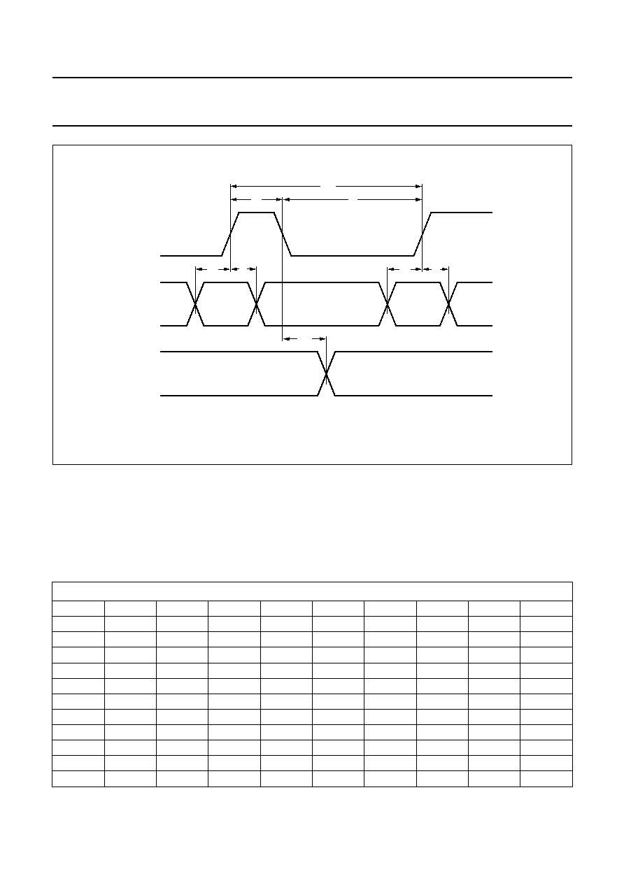
1997 Nov 17
56
Philips Semiconductors
Preliminary specification
ISO/MPEG Audio Source Decoder
SAA2502
11.1
Host interface: CDATA, CCLK and CMODE
For L3 mode host interface timing information is detailed in the Section 8.1.
The I
2
C-bus mode host interface timing is master clock dependent, adherence to this specification is only guaranteed for
the maximum MCLKIN frequency. If MCLKIN frequency is below maximum in principle all timing figures should be
increased proportionally.
Table 65 Supported REFCLK frequencies
REFCLK (kHz)
6
6.4
8
9.6
12
12.8
16
18
19.2
24
25.6
28.8
30
32
36
38.4
40
42
44.8
48
51.2
54
56
57.6
60
64
66
67.2
70.4
72
76.8
78
80
83.2
84
86.4
88
89.6
90
96
102
102.4
104
105.6
108
108.8
112
114
115.2
120
121.6
124.8
126
128
132
134.4
136
138
140.8
144
147.2
150
152
153.6
156
160
162
163.2
166.4
168
172.8
174
176
179.2
180
182.4
184
185.6
186
192
198.4
200
201.6
204
204.8
208
210
211.2
216
220.8
224
228
230.4
232
240
248
249.6
252
256
259.2
264
268.8
270
272
276
278.4
280
288
297.6
300
304
307.2
312
320
324
326.4
330
336
345.6
348
Fig.28 Timing diagram.
,,,,,,,
,,,,,,,
,,,,,,,
,,
,,
,,
,,,
,,,
,,,
handbook, full pagewidth
MGE487
CLOCK
INPUT
OUTPUT
tPD
tsu
th
tsu
th
tH
tL
Tcy

1997 Nov 17
57
Philips Semiconductors
Preliminary specification
ISO/MPEG Audio Source Decoder
SAA2502
352
360
364.8
368
372
384
390
400
403.2
408
416
420
422.4
432
440
441.6
448
450
456
460.8
464
480
496
499.2
504
510
512
518.4
520
528
537.6
540
544
552
556.8
560
570
576
595.2
600
608
614.4
624
630
640
648
660
672
680
690
696
704
720
736
744
750
760
768
780
800
810
816
832
840
864
870
880
896
900
912
920
928
930
960
992
1000
1008
1020
1024
1040
1050
1056
1080
1104
1120
1140
1152
1160
1200
1240
1248
1260
1280
1296
1320
1344
1350
1360
1380
1392
1400
1440
1488
1500
1520
1536
1560
1600
1620
1632
1650
1680
1728
1740
1760
1800
1824
1840
1860
1920
1950
2000
2016
2040
2080
2100
2112
2160
2200
2208
2240
2250
2280
2304
2320
2400
2480
2496
2520
2550
2560
2592
2600
2640
2688
2700
2720
2760
2784
2800
2850
2880
2976
3000
3040
3072
3120
3150
3200
3240
3300
3360
3400
3450
3480
3520
3600
3680
3720
3750
3800
3840
3900
4000
4050
4080
4160
4200
4320
4350
4400
4480
4500
4560
4600
4640
4650
4800
4960
5000
5040
5100
5120
5200
5250
5280
5400
5520
5600
5700
5760
5800
6000
6200
6240
6300
6400
6480
6600
6720
6750
6800
6900
6960
7000
7200
7440
7500
7600
7680
7800
8000
8100
8160
8250
8400
8640
8700
8800
9000
9120
9200
9300
9600
9750
10000
10080
10200
10400
10500
10560
10800
11000
11040
11200
11250
11400
11520
11600
12000
12400
12480
12600
12750
12800
12960
13000
13200
13440
13500
13600
13800
13920
14000
14250
14400
14880
15000
15200
15360
15600
15750
16000
16200
16500
16800
17000
17250
17400
17600
18000
18400
18600
18750
19000
19200
19500
20000
20250
20400
20800
21000
21600
21750
22000
22400
22500
22800
23000
23200
23250
24000
24800
25000
25200
25500
25600
26000
26400
27000
27600
28000
28500
28800
29000
30000
-
-
-
-
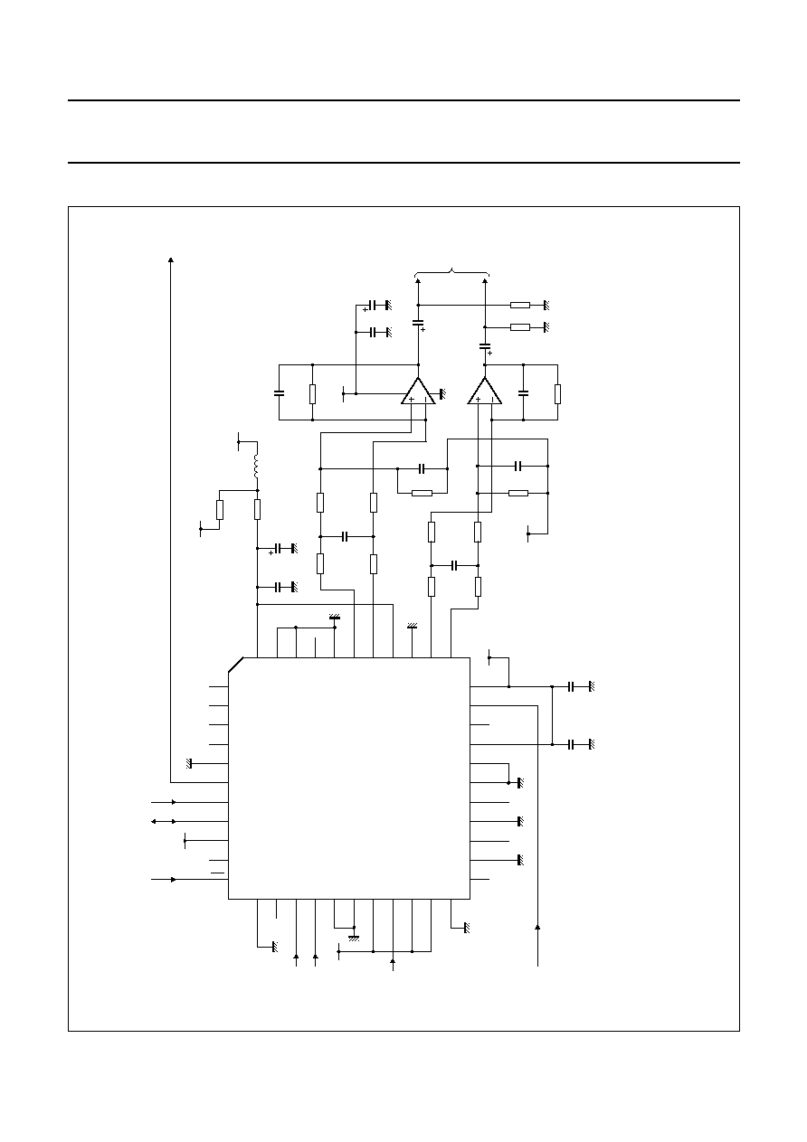
1997 Nov 17
58
Philips Semiconductors
Preliminary specification
ISO/MPEG Audio Source Decoder
SAA2502
12 APPLICATION INFORMATION
k, full pagewidth
MGG817
10 k
4.7
µ
H
C13
100
µ
F
11
k
R14
10 k
R7
10 k
C2
100
µ
F
C1
10 nF
C3
390 pF
C4
220
pF
U2
TDA1308T
C10
220
pF
C14
100 nF
C9
390
pF
STOP
CDRQ
CDCL
CD
GND1
CDEF
CDSY
V
DD1
CDVAL
TMS
REFCLK
PHDIF
RESET
INT
CMODE
CDATA
CCLK
SPDIF
TRST
WS
SD
SCK
FSCLK
TCK
FSCLKIN
X22IN
X22OUT
GND2
MCLK24
MLCKOUT
TDI
MLCKIN
reset
12.228 MHz
I
2
C-bus
data
I
2
C-bus
clock
11
12
13
14
15
16
17
18
19
20
21
22
44
43
42
41
40
39
38
37
36
35
34
V
DD3
VA1
L1
R16
R15
R1
10 k
11 k
R2
C6
10 nF
10 k
R3
10 k
R8
10 k
R9
R5
3
2
8
4
1
7
5
6
C11
C5
R6
VA1
220 pF
right
left
analog
R13
220 pF
11
k
R12
10 k
R10
10 k
R11
10 k
11 k
R4
+
5 V
+
5 V
+
5 V
+
5 V
+
2.5 V
4.7
4.7
SPDIF O/P
data
clock
sync
signal
data
TC1
GND3
TDO
TC0
LFTPOS
LFTNEG
REFP
REFN
RGTNEG
RGTPOS
1
0
9876
U1
SAA2502
54321
23
24
25
26
27
28
29
30
31
32
33
C8
100
µ
F
100
µ
F
C12
C7
100
µ
F
VDD2
Fig.29 Application circuit for ADR.
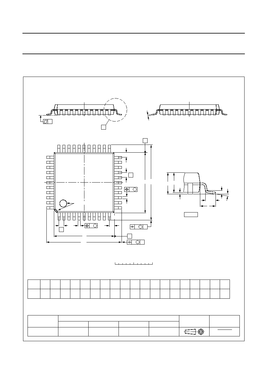
1997 Nov 17
59
Philips Semiconductors
Preliminary specification
ISO/MPEG Audio Source Decoder
SAA2502
13 PACKAGE OUTLINE
UNIT
A
1
A
2
A
3
b
p
c
E
(1)
e
H
E
L
L
p
Z
y
w
v
REFERENCES
OUTLINE
VERSION
EUROPEAN
PROJECTION
ISSUE DATE
IEC
JEDEC
EIAJ
mm
0.25
0.05
1.85
1.65
0.25
0.40
0.20
0.25
0.14
10.1
9.9
0.8
1.3
12.9
12.3
1.2
0.8
10
0
o
o
0.15
0.1
0.15
DIMENSIONS (mm are the original dimensions)
Note
1. Plastic or metal protrusions of 0.25 mm maximum per side are not included.
0.95
0.55
SOT307-2
95-02-04
97-08-01
D
(1)
(1)
(1)
10.1
9.9
H
D
12.9
12.3
E
Z
1.2
0.8
D
e
E
B
11
c
E
H
D
ZD
A
Z E
e
v
M
A
X
1
44
34
33
23
22
12
y
A
1
A
L
p
detail X
L
(A )
3
A
2
pin 1 index
D
H
v
M
B
b
p
b
p
w
M
w
M
0
2.5
5 mm
scale
QFP44: plastic quad flat package; 44 leads (lead length 1.3 mm); body 10 x 10 x 1.75 mm
SOT307-2
A
max.
2.10

1997 Nov 17
60
Philips Semiconductors
Preliminary specification
ISO/MPEG Audio Source Decoder
SAA2502
14 SOLDERING
14.1
Introduction
There is no soldering method that is ideal for all IC
packages. Wave soldering is often preferred when
through-hole and surface mounted components are mixed
on one printed-circuit board. However, wave soldering is
not always suitable for surface mounted ICs, or for
printed-circuits with high population densities. In these
situations reflow soldering is often used.
This text gives a very brief insight to a complex technology.
A more in-depth account of soldering ICs can be found in
our
"IC Package Databook" (order code 9398 652 90011).
14.2
Reflow soldering
Reflow soldering techniques are suitable for all QFP
packages.
The choice of heating method may be influenced by larger
plastic QFP packages (44 leads, or more). If infrared or
vapour phase heating is used and the large packages are
not absolutely dry (less than 0.1% moisture content by
weight), vaporization of the small amount of moisture in
them can cause cracking of the plastic body. For more
information, refer to the Drypack chapter in our
"Quality
Reference Handbook" (order code 9397 750 00192).
Reflow soldering requires solder paste (a suspension of
fine solder particles, flux and binding agent) to be applied
to the printed-circuit board by screen printing, stencilling or
pressure-syringe dispensing before package placement.
Several techniques exist for reflowing; for example,
thermal conduction by heated belt. Dwell times vary
between 50 and 300 seconds depending on heating
method. Typical reflow temperatures range from
215 to 250
∞
C.
Preheating is necessary to dry the paste and evaporate
the binding agent. Preheating duration: 45 minutes at
45
∞
C.
14.3
Wave soldering
Wave soldering is not recommended for QFP packages.
This is because of the likelihood of solder bridging due to
closely-spaced leads and the possibility of incomplete
solder penetration in multi-lead devices.
If wave soldering cannot be avoided, the following
conditions must be observed:
∑
A double-wave (a turbulent wave with high upward
pressure followed by a smooth laminar wave)
soldering technique should be used.
∑
The footprint must be at an angle of 45
∞
to the board
direction and must incorporate solder thieves
downstream and at the side corners.
Even with these conditions, do not consider wave
soldering the following packages: QFP52 (SOT379-1),
QFP100 (SOT317-1), QFP100 (SOT317-2),
QFP100 (SOT382-1) or QFP160 (SOT322-1).
During placement and before soldering, the package must
be fixed with a droplet of adhesive. The adhesive can be
applied by screen printing, pin transfer or syringe
dispensing. The package can be soldered after the
adhesive is cured.
Maximum permissible solder temperature is 260
∞
C, and
maximum duration of package immersion in solder is
10 seconds, if cooled to less than 150
∞
C within
6 seconds. Typical dwell time is 4 seconds at 250
∞
C.
A mildly-activated flux will eliminate the need for removal
of corrosive residues in most applications.
14.4
Repairing soldered joints
Fix the component by first soldering two diagonally-
opposite end leads. Use only a low voltage soldering iron
(less than 24 V) applied to the flat part of the lead. Contact
time must be limited to 10 seconds at up to 300
∞
C. When
using a dedicated tool, all other leads can be soldered in
one operation within 2 to 5 seconds between
270 and 320
∞
C.

1997 Nov 17
61
Philips Semiconductors
Preliminary specification
ISO/MPEG Audio Source Decoder
SAA2502
15 DEFINITIONS
16 LIFE SUPPORT APPLICATIONS
These products are not designed for use in life support appliances, devices, or systems where malfunction of these
products can reasonably be expected to result in personal injury. Philips customers using or selling these products for
use in such applications do so at their own risk and agree to fully indemnify Philips for any damages resulting from such
improper use or sale.
Data sheet status
Objective specification
This data sheet contains target or goal specifications for product development.
Preliminary specification
This data sheet contains preliminary data; supplementary data may be published later.
Product specification
This data sheet contains final product specifications.
Limiting values
Limiting values given are in accordance with the Absolute Maximum Rating System (IEC 134). Stress above one or
more of the limiting values may cause permanent damage to the device. These are stress ratings only and operation
of the device at these or at any other conditions above those given in the Characteristics sections of the specification
is not implied. Exposure to limiting values for extended periods may affect device reliability.
Application information
Where application information is given, it is advisory and does not form part of the specification.

1997 Nov 17
62
Philips Semiconductors
Preliminary specification
ISO/MPEG Audio Source Decoder
SAA2502
NOTES

1997 Nov 17
63
Philips Semiconductors
Preliminary specification
ISO/MPEG Audio Source Decoder
SAA2502
NOTES

Internet: http://www.semiconductors.philips.com
Philips Semiconductors ≠ a worldwide company
© Philips Electronics N.V. 1997
SCA56
All rights are reserved. Reproduction in whole or in part is prohibited without the prior written consent of the copyright owner.
The information presented in this document does not form part of any quotation or contract, is believed to be accurate and reliable and may be changed
without notice. No liability will be accepted by the publisher for any consequence of its use. Publication thereof does not convey nor imply any license
under patent- or other industrial or intellectual property rights.
Netherlands: Postbus 90050, 5600 PB EINDHOVEN, Bldg. VB,
Tel. +31 40 27 82785, Fax. +31 40 27 88399
New Zealand: 2 Wagener Place, C.P.O. Box 1041, AUCKLAND,
Tel. +64 9 849 4160, Fax. +64 9 849 7811
Norway: Box 1, Manglerud 0612, OSLO,
Tel. +47 22 74 8000, Fax. +47 22 74 8341
Philippines: Philips Semiconductors Philippines Inc.,
106 Valero St. Salcedo Village, P.O. Box 2108 MCC, MAKATI,
Metro MANILA, Tel. +63 2 816 6380, Fax. +63 2 817 3474
Poland: Ul. Lukiska 10, PL 04-123 WARSZAWA,
Tel. +48 22 612 2831, Fax. +48 22 612 2327
Portugal: see Spain
Romania: see Italy
Russia: Philips Russia, Ul. Usatcheva 35A, 119048 MOSCOW,
Tel. +7 095 755 6918, Fax. +7 095 755 6919
Singapore: Lorong 1, Toa Payoh, SINGAPORE 1231,
Tel. +65 350 2538, Fax. +65 251 6500
Slovakia: see Austria
Slovenia: see Italy
South Africa: S.A. PHILIPS Pty Ltd., 195-215 Main Road Martindale,
2092 JOHANNESBURG, P.O. Box 7430 Johannesburg 2000,
Tel. +27 11 470 5911, Fax. +27 11 470 5494
South America: Al. Vicente Pinzon, 173, 6th floor,
04547-130 S√O PAULO, SP, Brazil,
Tel. +55 11 821 2333, Fax. +55 11 821 2382
Spain: Balmes 22, 08007 BARCELONA,
Tel. +34 3 301 6312, Fax. +34 3 301 4107
Sweden: Kottbygatan 7, Akalla, S-16485 STOCKHOLM,
Tel. +46 8 632 2000, Fax. +46 8 632 2745
Switzerland: Allmendstrasse 140, CH-8027 ZÐRICH,
Tel. +41 1 488 2686, Fax. +41 1 481 7730
Taiwan: Philips Semiconductors, 6F, No. 96, Chien Kuo N. Rd., Sec. 1,
TAIPEI, Taiwan Tel. +886 2 2134 2865, Fax. +886 2 2134 2874
Thailand: PHILIPS ELECTRONICS (THAILAND) Ltd.,
209/2 Sanpavuth-Bangna Road Prakanong, BANGKOK 10260,
Tel. +66 2 745 4090, Fax. +66 2 398 0793
Turkey: Talatpasa Cad. No. 5, 80640 GÐLTEPE/ISTANBUL,
Tel. +90 212 279 2770, Fax. +90 212 282 6707
Ukraine: PHILIPS UKRAINE, 4 Patrice Lumumba str., Building B, Floor 7,
252042 KIEV, Tel. +380 44 264 2776, Fax. +380 44 268 0461
United Kingdom: Philips Semiconductors Ltd., 276 Bath Road, Hayes,
MIDDLESEX UB3 5BX, Tel. +44 181 730 5000, Fax. +44 181 754 8421
United States: 811 East Arques Avenue, SUNNYVALE, CA 94088-3409,
Tel. +1 800 234 7381
Uruguay: see South America
Vietnam: see Singapore
Yugoslavia: PHILIPS, Trg N. Pasica 5/v, 11000 BEOGRAD,
Tel. +381 11 625 344, Fax.+381 11 635 777
For all other countries apply to: Philips Semiconductors,
International Marketing & Sales Communications, Building BE-p,
P.O. Box 218, 5600 MD EINDHOVEN, The Netherlands, Fax. +31 40 27 24825
Argentina: see South America
Australia: 34 Waterloo Road, NORTH RYDE, NSW 2113,
Tel. +61 2 9805 4455, Fax. +61 2 9805 4466
Austria: Computerstr. 6, A-1101 WIEN, P.O. Box 213, Tel. +43 160 1010,
Fax. +43 160 101 1210
Belarus: Hotel Minsk Business Center, Bld. 3, r. 1211, Volodarski Str. 6,
220050 MINSK, Tel. +375 172 200 733, Fax. +375 172 200 773
Belgium: see The Netherlands
Brazil: see South America
Bulgaria: Philips Bulgaria Ltd., Energoproject, 15th floor,
51 James Bourchier Blvd., 1407 SOFIA,
Tel. +359 2 689 211, Fax. +359 2 689 102
Canada: PHILIPS SEMICONDUCTORS/COMPONENTS,
Tel. +1 800 234 7381
China/Hong Kong: 501 Hong Kong Industrial Technology Centre,
72 Tat Chee Avenue, Kowloon Tong, HONG KONG,
Tel. +852 2319 7888, Fax. +852 2319 7700
Colombia: see South America
Czech Republic: see Austria
Denmark: Prags Boulevard 80, PB 1919, DK-2300 COPENHAGEN S,
Tel. +45 32 88 2636, Fax. +45 31 57 0044
Finland: Sinikalliontie 3, FIN-02630 ESPOO,
Tel. +358 9 615800, Fax. +358 9 61580920
France: 51 Rue Carnot, BP317, 92156 SURESNES Cedex,
Tel. +33 1 40 99 6161, Fax. +33 1 40 99 6427
Germany: Hammerbrookstraþe 69, D-20097 HAMBURG,
Tel. +49 40 23 53 60, Fax. +49 40 23 536 300
Greece: No. 15, 25th March Street, GR 17778 TAVROS/ATHENS,
Tel. +30 1 4894 339/239, Fax. +30 1 4814 240
Hungary: see Austria
India: Philips INDIA Ltd, Band Box Building, 2nd floor,
254-D, Dr. Annie Besant Road, Worli, MUMBAI 400 025,
Tel. +91 22 493 8541, Fax. +91 22 493 0966
Indonesia: see Singapore
Ireland: Newstead, Clonskeagh, DUBLIN 14,
Tel. +353 1 7640 000, Fax. +353 1 7640 200
Israel: RAPAC Electronics, 7 Kehilat Saloniki St, PO Box 18053,
TEL AVIV 61180, Tel. +972 3 645 0444, Fax. +972 3 649 1007
Italy: PHILIPS SEMICONDUCTORS, Piazza IV Novembre 3,
20124 MILANO, Tel. +39 2 6752 2531, Fax. +39 2 6752 2557
Japan: Philips Bldg 13-37, Kohnan 2-chome, Minato-ku, TOKYO 108,
Tel. +81 3 3740 5130, Fax. +81 3 3740 5077
Korea: Philips House, 260-199 Itaewon-dong, Yongsan-ku, SEOUL,
Tel. +82 2 709 1412, Fax. +82 2 709 1415
Malaysia: No. 76 Jalan Universiti, 46200 PETALING JAYA, SELANGOR,
Tel. +60 3 750 5214, Fax. +60 3 757 4880
Mexico: 5900 Gateway East, Suite 200, EL PASO, TEXAS 79905,
Tel. +9-5 800 234 7381
Middle East: see Italy
Printed in The Netherlands
547027/00/02/pp64
Date of release: 1997 Nov 17
Document order number:
9397 750 03068