 | ÐлекÑÑоннÑй компоненÑ: SAA3010 | СкаÑаÑÑ:  PDF PDF  ZIP ZIP |
Äîêóìåíòàöèÿ è îïèñàíèÿ www.docs.chipfind.ru

DATA SHEET
Product specification
File under Integrated Circuits, IC01
June 1989
INTEGRATED CIRCUITS
SAA3010
Infrared remote control transmitter
RC-5

June 1989
2
Philips Semiconductors
Product specification
Infrared remote control transmitter RC-5
SAA3010
FEATURES
·
Low voltage requirement
·
Biphase transmission technique
·
Single pin oscillator
·
Test mode facility
GENERAL DESCRIPTION
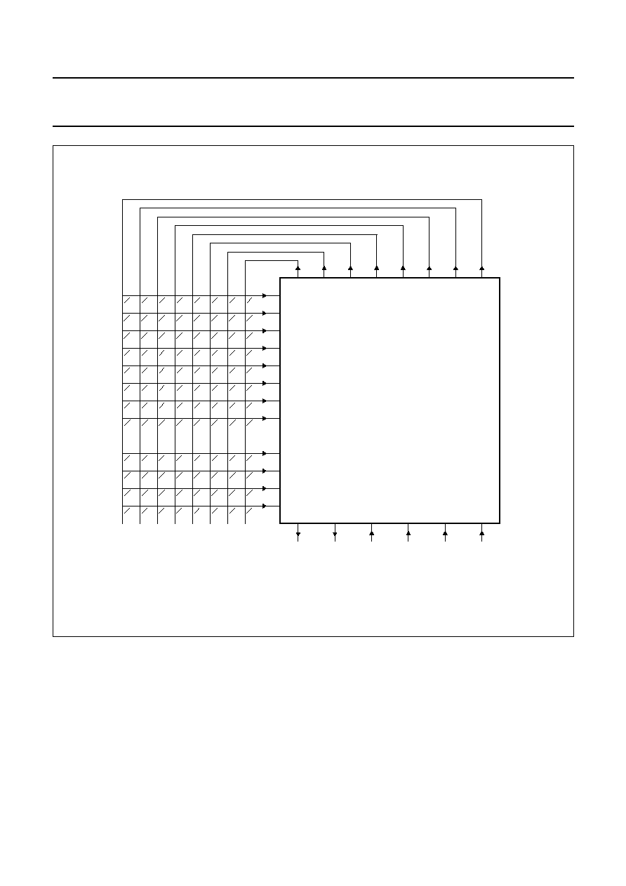
The SAA3010 is intended as a general purpose (RC-5)
infrared remote control system for use where a low voltage
supply and a large debounce time are expected.
The device can generate 2048 different commands and
utilizes a keyboard with a single pole switch for each key.
The commands are arranged so that 32 systems can be
addressed, each system containing 64 different
commands. The keyboard interconnection is illustrated by
Fig.3.
The circuit response to legal (one key pressed at a time)
and illegal (more than one key pressed at a time) keyboard
operation is specified in the section "Keyboard operation".
QUICK REFERENCE DATA
Note
1. V
DD
+0.5 V must not exceed 9 V.
PACKAGE OUTLINES
28-lead DIL plastic; (SOT117); SOT117-1; 1996 September 11.
28-lead mini-pack; plastic (SO28; SOT136A); SOT136-1; 1996 September 11.
PARAMETER
SYMBOL
MIN.
TYP.
MAX.
UNIT
Supply voltage range
V
DD
2
-
7
V
Input voltage range (note 1)
V
I
-
0.5
-
V
DD
+0.5
V
Input current
I
I
-
-
±
10
mA
Output voltage range (note 1)
V
O
-
0.5
-
V
DD
+0.5
V
Output current
I
O
-
-
±
10
mA
Operating ambient temperature
range
T
amb
-
25
-
85
°
C
WARNING
The use of this device must conform with the Philips Standard number URT-0421.
June 1989
3
Philips Semiconductors
Product specification
Infrared remote control transmitter RC-5
SAA3010
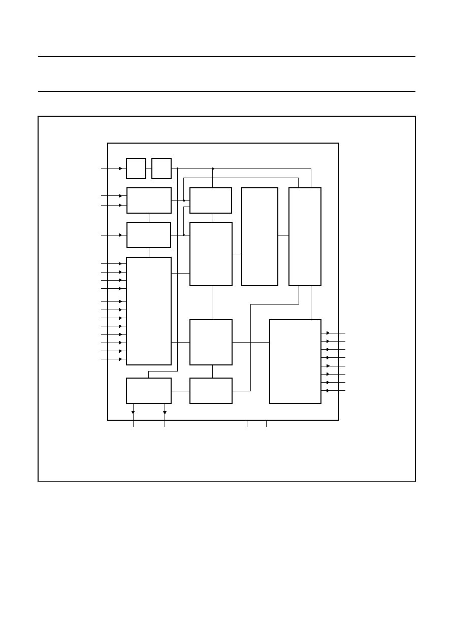
BLOCK DIAGRAM
handbook, full pagewidth
MGE347
KEYBOARD
ENCODER
MODE
SELECTION
TEST
MODE
OSC
3
×
2
1
OUTPUT
COMMAND
AND
SYSTEM
ADDRESS
LATCH
PARALLEL
TO SERIAL
CONVERTER
MASTER
RESET
GENERATOR
CONTROL
UNIT
DECODER
2
13
DIVIDER
KEYBOARD
DRIVER
DECODER
18
20
19
2
6
5
4
3
1
27
26
25
24
23
22
21
8
7
17
16
15
13
12
11
10
9
14
28
SAA3010
OSC
TP1
TP2
SSM
Z3
Z2
Z1
Z0
X7
X6
X5
X4
X3
X2
X1
X0
DATA
MDATA
VSS
VDD
DR0
DR1
DR2
DR3
DR4
DR5
DR6
DR7
Fig.1 Block diagram.
June 1989
4
Philips Semiconductors
Product specification
Infrared remote control transmitter RC-5
SAA3010
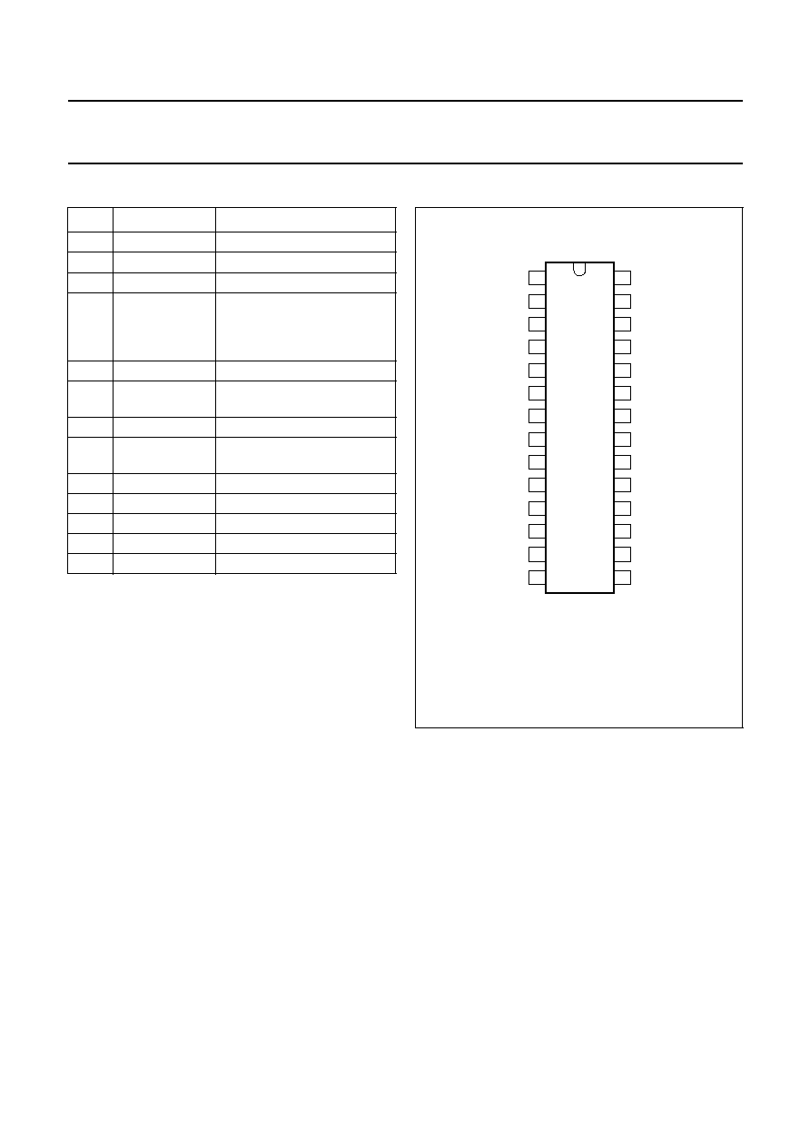
PINNING
Note
1. (I) = input
(IPU) = input with p-channel pull-up transistor
(ODN) = output with open drain n-channel transistor
(OP3) = output 3-state
PIN
MNEMONIC
(1)
FUNCTION
1
X7 (IPU)
sense input from key matrix
2
SSM (I)
system mode selection input
3-6
Z0-Z3 (IPU)
sense inputs from key matrix
7
MDATA (OP3)
generated output data
modulated with 1/12 the
oscillator frequency at a 25%
duty factor
8
DATA (OP3)
generated output information
9-13
DR7-DR3
(ODN)
scan drivers
14
V
SS
ground (0 V)
15-17
DR2-DR0
(ODN)
scan drivers
18
OSC (I)
oscillator input
19
TP2 (I)
test point 2
20
TP1 (I)
test point 1
21-27
X0-X6 (IPU)
sense inputs from key matrix
28
V
DD
(I)
voltage supply
handbook, halfpage
X7
SSM
Z0
Z1
Z2
Z3
MDATA
DATA
DR7
DR6
DR5
DR4
DR3
VSS
VDD
X6
X5
X4
X2
X1
X3
X0
TP1
TP2
OSC
DR0
DR1
DR2
1
2
3
4
5
6
7
8
9
10
11
12
13
28
27
26
25
24
23
22
21
20
19
18
17
16
15
14
SAA3010
MGE346
Fig.2 Pinning diagram.
June 1989
5
Philips Semiconductors
Product specification
Infrared remote control transmitter RC-5
SAA3010
Fig.3 Keyboard interconnection.
handbook, full pagewidth
Z0
Z1
Z2
Z3
X0
X1
X2
X3
X4
X5
X6
X7
DR0
DR1
DR2
DR3
DR4
DR5
DR6
DR7
DATA
MDATA
SSM
TP1
TP2
OSC
MGE348
17
16
15
13
12
11
10
9
21
22
23
24
25
26
27
1
3
4
5
6
8
7
2
20
19
18
SAA3010

June 1989
6
Philips Semiconductors
Product specification
Infrared remote control transmitter RC-5
SAA3010
FUNCTIONAL DESCRIPTION
Keyboard operation
Every connection of one X-input and one DR-output will be recognized as a legal key operation and will cause the device
to generate the corresponding code. The same applies to every connection of one Z-input to one DR-output with the
proviso that SSM must be LOW. When SSM is HIGH a wired connection must exist between a Z-input and a DR-output.
If no connection is present the system number will not be generated. Activating two or more X-inputs, Z-inputs or Z-inputs
and X-inputs at the same time is an illegal action and inhibits further activity (oscillator will not start).
When one X- or Z-input is connected to more than one DR-output, the last scan signal will be considered as legal.
The maximum value of the contact series resistance of the switched keyboard is 7 k
.
Inputs
In the quiescent state the command inputs X0 to X7 are held HIGH by an internal pull-up transistor. When the system
mode selection (SSM) input is LOW and the system is quiescent, the system inputs Z0 to Z3 are also held HIGH by an
internal pull-up transistor. When SSM is HIGH the pull-up transistor for the Z-inputs is switched off, in order to prevent
current flow, and a wired connection in the Z-DR matrix provides the system number.
Outputs
The output signal DATA transmits the generated information in accordance with the format illustrated by Fig.4 and
Tables 1 and 2. The code is transmitted using a biphase technique as illustrated by Fig.5. The code consists of four parts:
·
Start part
-
1.5 bits (2
×
logic 1)
·
Control part
-
1 bit
·
System part
-
5 bits
·
Command part
-
6 bits
The output signal MDATA transmits the generated information modulated by 1/12 of the oscillator frequency with a 50%
duty factor.
In the quiescent state both DATA and MDATA are non-conducting (3-state outputs).
The scan driver outputs DR0 to DR7 are open drain n-channel transistors and conduct when the circuit is quiescent.
After a legal key operation the scanning cycle is started and the outputs switched to the conductive state one by one.
The DR-outputs were switched off at the end of the preceding debounce cycle.
June 1989
7
Philips Semiconductors
Product specification
Infrared remote control transmitter RC-5
SAA3010
Fig.4 Data output format.
Where:
debounce time + scan time = 18 bit-times
repetition time = 4
×
16 bit-times
handbook, full pagewidth
MGE349
debounce
time
(16 bit-times)
scan
time
start
bits
control
bit
system bits
command bits
1st. code
2nd. code
TWO SUCCESSIVE CODES
MSB
LSB MSB
LSB
start
start
ONE CODE
Fig.5 Biphase transmission technique.
Where:
1 bit-time = 3.2
8
×
T
OSC
= 1.778 ms (typ.)
handbook, halfpage
MGE350
logic 1
logic 0

June 1989
8
Philips Semiconductors
Product specification
Infrared remote control transmitter RC-5
SAA3010
Table 1
Command matrix (X-DR)
CODE
NO.
X-LINES
DR-LINES
COMMAND BITS
0
1
2
3
4
5
6
7
0
1
2
3
4
5
6
7
5
4
3
2
1
0
0
·
·
0
0
0
0
0
0
1
·
·
0
0
0
0
0
1
2
·
·
0
0
0
0
1
0
3
·
·
0
0
0
0
1
1
4
·
·
0
0
0
1
0
0
5
·
·
0
0
0
1
0
1
6
·
·
0
0
0
1
1
0
7
·
·
0
0
0
1
1
1
8
·
·
0
0
1
0
0
0
9
·
·
0
0
1
0
0
1
10
·
·
0
0
1
0
1
0
11
·
·
0
0
1
0
1
1
12
·
·
0
0
1
1
0
0
13
·
·
0
0
1
1
0
1
14
·
·
0
0
1
1
1
0
15
·
·
0
0
1
1
1
1
16
·
·
0
1
0
0
0
0
17
·
·
0
1
0
0
0
1
18
·
·
0
1
0
0
1
0
19
·
·
0
1
0
0
1
1
20
·
·
0
1
0
1
0
0
21
·
·
0
1
0
1
0
1
22
·
·
0
1
0
1
1
0
23
·
·
0
1
0
1
1
1
24
·
·
0
1
1
0
0
0
25
·
·
0
1
1
0
0
1
26
·
·
0
1
1
0
1
0
27
·
·
0
1
1
0
1
1
28
·
·
0
1
1
1
0
0
29
·
·
0
1
1
1
0
1
30
·
·
0
1
1
1
1
0
31
·
·
0
1
1
1
1
1

June 1989
9
Philips Semiconductors
Product specification
Infrared remote control transmitter RC-5
SAA3010
32
·
·
1
0
0
0
0
0
33
·
·
1
0
0
0
0
1
34
·
·
1
0
0
0
1
0
35
·
·
1
0
0
0
1
1
36
·
·
1
0
0
1
0
0
37
·
·
1
0
0
1
0
1
38
·
·
1
0
0
1
1
0
39
·
·
1
0
0
1
1
1
40
·
·
1
0
1
0
0
0
41
·
·
1
0
1
0
0
1
42
·
·
1
0
1
0
1
0
43
·
·
1
0
1
0
1
1
44
·
·
1
0
1
1
0
0
45
·
·
1
0
1
1
0
1
46
·
·
1
0
1
1
1
0
47
·
·
1
0
1
1
1
1
48
·
·
1
1
0
0
0
0
49
·
·
1
1
0
0
0
1
50
·
·
1
1
0
0
1
0
51
·
·
1
1
0
0
1
1
52
·
·
1
1
0
1
0
0
53
·
·
1
1
0
1
0
1
54
·
·
1
1
0
1
1
0
55
·
·
1
1
0
1
1
1
56
· ·
1
1
1
0
0
0
57
·
·
1
1
1
0
0
1
58
·
·
1
1
1
0
1
0
59
·
·
1
1
1
0
1
1
60
·
·
1
1
1
1
0
0
61
·
·
1
1
1
1
0
1
62
·
·
1
1
1
1
1
0
63
·
·
1
1
1
1
1
1
CODE
NO.
X-LINES
DR-LINES
COMMAND BITS
0
1
2
3
4
5
6
7
0
1
2
3
4
5
6
7
5
4
3
2
1
0

June 1989
10
Philips Semiconductors
Product specification
Infrared remote control transmitter RC-5
SAA3010
Table 2
System matrix (Z-DR)
SYST.
NO.
Z-LINES
DR-LINES
SYSTEM BITS
0
1
2
3
4
5
6
7
0
1
2
3
4
5
6
7
4
3
2
1
0
0
·
·
0
0
0
0
0
1
·
·
0
0
0
0
1
2
·
·
0
0
0
1
0
3
·
·
0
0
0
1
1
4
·
·
0
0
1
0
0
5
·
·
0
0
1
0
1
6
·
·
0
0
1
1
0
7
·
·
0
0
1
1
1
8
·
·
0
1
0
0
0
9
·
·
0
1
0
0
1
10
·
·
0
1
0
1
0
11
·
·
0
1
0
1
1
12
·
·
0
1
1
0
0
13
·
·
0
1
1
0
1
14
·
·
0
1
1
1
0
15
·
·
0
1
1
1
1
16
·
·
1
0
0
0
0
17
·
·
1
0
0
0
1
18
·
·
1
0
0
1
0
19
·
·
1
0
0
1
1
20
·
·
1
0
1
0
0
21
·
·
1
0
1
0
1
22
·
·
1
0
1
1
0
23
·
·
1
0
1
1
1
24
·
·
1
1
0
0
0
25
·
·
1
1
0
0
1
26
·
·
1
1
0
1
0
27
·
·
1
1
0
1
1
28
·
·
1
1
1
0
0
29
·
·
1
1
1
0
1
30
·
·
1
1
1
1
0
31
·
·
1
1
1
1
1

June 1989
11
Philips Semiconductors
Product specification
Infrared remote control transmitter RC-5
SAA3010
Combined system mode (SSM is LOW)
The X and Z sense inputs have p-channel pull-up transistors, so that they are HIGH, until pulled LOW by connecting them
to an output as the result of a key operation. Legal operation of a key in the X-DR or Z-DR matrix will start the debounce
cycle, once key contact has been established for 18 bit-times without interruption, the oscillator enable signal is latched
and the key may be released. An interruption within the 18 bit-time period resets the device.
At the end of the debounce cycle the DR-outputs are switched off and two scan cycles are started, that switch on the
DR-lines one by one. When a Z- or X-input senses a low level, a latch enable signal is fed to the system (Z-input) or
command (X-input) latches.
After latching a system number the device will generate the last command (i.e. all command bits logic 1) in the chosen
system for as long as the key is operated. Latching of a command number causes the chip to generate this command
together with the system number memorized in the system latch. Releasing the key will reset the device if no data is to
be transmitted at the time. Once transmission has started the code will complete to the end.
Single system mode (SSM is HIGH)
In the single system mode, the X-inputs will be HIGH as in the combined system mode. The Z-inputs will be disabled by
having their pull-up transistors switched off; a wired connection in the Z-DR matrix provides the system code. Only legal
key operation in the X-DR matrix will start the debounce cycle, once key contact has been established for 18 bit-times
without interruption the oscillator enable signal is latched and the key may be released. An interruption within the
18 bit-time period resets the internal action.
At the end of the debounce cycle the pull-up transistors in the X-lines are switched off and those in the Z-lines are
switched on for the first scan cycle. The wired connection in the Z-matrix is then translated into a system number and
memorized in the system latch. At the end of the first scan cycle the pull-up transistors in the Z-lines are switched off and
the inputs are disabled again; the pull-up transistors in the X-lines are switched on. The second scan cycle produces the
command number which, after being latched, is transmitted together with the system number.
Key release detection
An extra control bit is added which will be complemented after key release; this indicates to the decoder that the next
code is a new command. This is important in the case where more digits need to be entered (channel numbers of Teletext
or Viewdata pages). The control bit will only be complemented after the completion of at least one code transmission.
The scan cycles are repeated before every code transmission, so that even with "take over" of key operation during code
transmission the right system and command numbers are generated.
Reset action
The device will be reset immediately a key is released during:
·
debounce time
·
between two codes.
When a key is released during matrix scanning, a reset will occur if:
·
a key is released while one of the driver outputs is in the low ohmic stage (logic 0)
·
a key is released before that key has been detected
·
there is no wired connection in the Z-DR matrix when SSM is HIGH.

June 1989
12
Philips Semiconductors
Product specification
Infrared remote control transmitter RC-5
SAA3010
Oscillator
The OSC is the input/output for a 1-pin oscillator. The oscillator is formed by a ceramic resonator, TOKO CRK429, order
code, 2422 540 98069 or equivalent. A resistor of 6.8 k
must be placed in series with the resonator. The resistor and
resonator are grounded at one side.
Test
Initialization of the circuit is performed when TP1, TP2 and OSC are HIGH. All internal nodes are defined except for the
LATCH. The latch is defined when a scan cycle is started by pulling down an X- or Z-input while the oscillator is running.
If the debounce cycle has been completed, the scan cycle can be completed 3
×
2
3
faster, by setting TP1 HIGH.
If the scan cycle has been completed, the contents of the latch can be read 3
×
2
7
faster by setting TP2 HIGH.

June 1989
13
Philips Semiconductors
Product specification
Infrared remote control transmitter RC-5
SAA3010
LIMITING VALUES
Limiting values in accordance with the Absolute Maximum Rating System (IEC 134)
Note
1. V
DD
+0.5 V must not exceed 9.0 V.
HANDLING
Inputs and outputs are protected against electrostatic charge in normal handling, however, to be totally safe it is desirable
to take normal precautions appropriate to handling MOS devices (see "Handling MOS Devices").
PARAMETER
SYMBOL
MIN.
MAX.
UNIT
Supply voltage range
V
DD
-
0.5
8.5
V
Input voltage range (note 1)
V
I
-
0.5
V
DD
+0.5
V
Output voltage range (note 1)
V
O
-
0.5
V
DD
+0.5
V
Input current
I
I
-
±
10
mA
Output current
I
O
-
±
10
mA
Maximum power dissipation
OSC output
P
O
-
50
mW
other outputs
P
O
-
100
mW
Total power dissipation
P
tot
-
200
mW
Operating ambient temperature range
T
amb
-
25
+85
°
C
Storage temperature range
T
stg
-
55
+150
°
C

June 1989
14
Philips Semiconductors
Product specification
Infrared remote control transmitter RC-5
SAA3010
DC CHARACTERISTICS
T
amb
=
-
25
°
C to +70
°
C; V
DD
= 2.0 to 7.0 V unless otherwise specified
PARAMETER
CONDITIONS
SYMBOL
MIN.
TYP.
MAX.
UNIT
Supply voltage
V
DD
2.0
-
7.0
V
Quiescent supply current
note 1
T
amb
= 25
°
C; I
O
= 0 mA at all
outputs; X0 to X7 and Z0 to
Z3 at V
DD
; TP1, TP2, OSC at
V
SS
SSM at V
SS
or V
DD
I
DD
-
-
10
µ
A
INPUTS
Keyboard inputs X and Z with
p-channel pull-up transistor
Input current at each input
V
I
= 0 V;
TP1 = TP2 = SSM = LOW
-
I
I
10
-
600
µ
A
Input voltage HIGH
note 2
V
IH
0.7V
DD
-
V
DD
V
Input voltage LOW
note 2
V
IL
0
-
0.3V
DD
V
Input leakage current
T
amb
= 25
°
C; V
I
= 7 V;
TP1 = TP2 = HIGH
I
LI
-
-
1
µ
A
Input leakage current
T
amb
= 25
°
C; V
I
= 0 V;
TP1 = TP2 = HIGH
-
I
LI
-
-
1
µ
A
OSC
Input leakage current
T
amb
= 25
°
C; V
I
= 0 V;
TP1 = TP2 = HIGH
-
I
LI
-
-
2
µ
A
Input current
T
amb
= 25
°
C; V
I
= V
DD
I
OSC
4.5
-
30
µ
A
SSM, TP1, TP2
Input voltage HIGH
V
IH
0.7V
DD
-
V
DD
V
Input voltage LOW
V
IL
0
-
0.3V
DD
V
Input leakage current
T
amb
= 25
°
C; V
I
= 7.0 V
I
LI
-
-
1
µ
A
Input leakage current
T
amb
= 25
°
C; V
I
= 0 V
-
I
LI
-
-
1
µ
A

June 1989
15
Philips Semiconductors
Product specification
Infrared remote control transmitter RC-5
SAA3010
Notes to the DC characteristics
1. Quiescent supply current measurement must be preceded by the initialization procedure described in the "Test"
section.
2. This DC test condition protects the AC performance of the output. The DC current requirements in the actual
applications are lower.
OUTPUTS
DATA, MDATA
Output voltage HIGH
I
OH
=
-
0.4 mA
V
OH
V
DD
-
0.3
-
-
V
Output voltage LOW
I
OL
= 0.6 mA
V
OL
-
-
0.3
V
Output leakage current
V
O
= 7.0 V
+I
LO
-
-
10
µ
A
V
O
= 7.0 V; T
amb
= 25
°
C
+I
LO
-
-
1
µ
A
V
O
= 0 V
-
I
LO
-
-
20
µ
A
V
O
= 0 V; T
amb
= 25
°
C
-
I
LO
-
-
2
µ
A
DR0
TO
DR7
Output voltage low
I
OL
= 0.3 mA
V
OL
-
-
0.3
V
Output leakage current
V
O
= 7.0 V
+I
LO
-
-
10
µ
A
V
O
= 7.0 V; T
amb
= 25
°
C
+I
LO
-
-
1
µ
A
PARAMETER
CONDITIONS
SYMBOL
MIN.
TYP.
MAX.
UNIT
June 1989
16
Philips Semiconductors
Product specification
Infrared remote control transmitter RC-5
SAA3010
AC CHARACTERISTICS
T
amb
=
-
25 to +85
°
C; V
DD
= 2.0 to 7.0 V unless otherwise stated.
PARAMETER
CONDITIONS SYMBOL
MIN.
TYP.
MAX.
UNIT
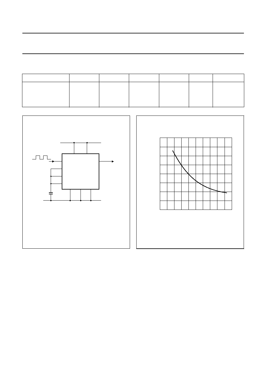
Oscillator frequency
C
L
= 160 pF;
Figs 6 and 7
operational
f
OSC
-
-
450
kHz
free-running
f
OSC
10
-
120
kHz
Fig.6 Test set-up for maximum f
OSC
measurement.
handbook, halfpage
MGE351
18
21
3
17
28
2
20
SAA3010
19
14
8
DATA
X0
Z0
DR0
TP1
TP2
VSS
VSS
SSM
VDD
OSC
VDD
160 pF
CL
Fig.7
Typical normalized frequency as a function of
keyboard load capacitance.
handbook, halfpage
0
2
1
0
80
400
MGE352
160
240
320
normalized
frequency
(kHz)
CL (pF)
June 1989
17
Philips Semiconductors
Product specification
Infrared remote control transmitter RC-5
SAA3010
PACKAGE OUTLINES
UNIT
A
max.
1
2
b
1
(1)
(1)
(1)
c
D
E
w
e
M
H
L
REFERENCES
OUTLINE
VERSION
EUROPEAN
PROJECTION
ISSUE DATE
IEC
JEDEC
EIAJ
mm
inches
DIMENSIONS (inch dimensions are derived from the original mm dimensions)
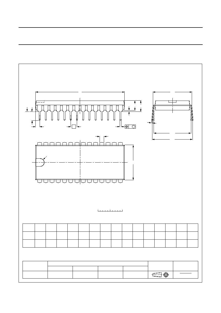
SOT117-1
92-11-17
95-01-14
A
min.
A
max.
b
Z
max.
M
E
e
1
1.7
1.3
0.53
0.38
0.32
0.23
36.0
35.0
14.1
13.7
3.9
3.4
0.25
2.54
15.24
15.80
15.24
17.15
15.90
1.7
5.1
0.51
4.0
0.066
0.051
0.020
0.014
0.013
0.009
1.41
1.34
0.56
0.54
0.15
0.13
0.01
0.10
0.60
0.62
0.60
0.68
0.63
0.067
0.20
0.020
0.16
051G05
MO-015AH
M
H
c
(e )
1
M
E
A
L
seating plane
A
1
w
M
b
1
e
D
A
2
Z
28
1
15
14
b
E
pin 1 index
0
5
10 mm
scale
Note
1. Plastic or metal protrusions of 0.25 mm maximum per side are not included.
handbook, full pagewidth
DIP28: plastic dual in-line package; 28 leads (600 mil)
SOT117-1
June 1989
18
Philips Semiconductors
Product specification
Infrared remote control transmitter RC-5
SAA3010
UNIT
A
max.
A
1
A
2
A
3
b
p
c
D
(1)
E
(1)
(1)
e
H
E
L
L
p
Q
Z
y
w
v
REFERENCES
OUTLINE
VERSION
EUROPEAN
PROJECTION
ISSUE DATE
IEC
JEDEC
EIAJ
mm
inches
2.65
0.30
0.10
2.45
2.25
0.49
0.36
0.32
0.23
18.1
17.7
7.6
7.4
1.27
10.65
10.00
1.1
1.0
0.9
0.4
8
0
o
o
0.25
0.1
DIMENSIONS (inch dimensions are derived from the original mm dimensions)
Note
1. Plastic or metal protrusions of 0.15 mm maximum per side are not included.
1.1
0.4
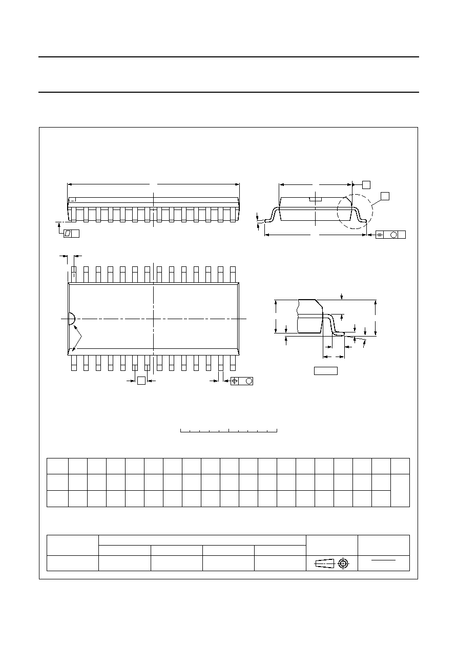
SOT136-1
X
14
28
w
M
A
A
1
A
2
b
p
D
H
E
L
p
Q
detail X
E
Z
c
L
v
M
A
e
15
1
(A )
3
A
y
0.25
075E06
MS-013AE
pin 1 index
0.10
0.012
0.004
0.096
0.089
0.019
0.014
0.013
0.009
0.71
0.69
0.30
0.29
0.050
1.4
0.055
0.419
0.394
0.043
0.039
0.035
0.016
0.01
0.25
0.01
0.004
0.043
0.016
0.01
0
5
10 mm
scale
SO28: plastic small outline package; 28 leads; body width 7.5 mm
SOT136-1
95-01-24
97-05-22

June 1989
19
Philips Semiconductors
Product specification
Infrared remote control transmitter RC-5
SAA3010
SOLDERING
Introduction
There is no soldering method that is ideal for all IC
packages. Wave soldering is often preferred when
through-hole and surface mounted components are mixed
on one printed-circuit board. However, wave soldering is
not always suitable for surface mounted ICs, or for
printed-circuits with high population densities. In these
situations reflow soldering is often used.
This text gives a very brief insight to a complex technology.
A more in-depth account of soldering ICs can be found in
our
"IC Package Databook" (order code 9398 652 90011).
DIP
S
OLDERING BY DIPPING OR BY WAVE
The maximum permissible temperature of the solder is
260
°
C; solder at this temperature must not be in contact
with the joint for more than 5 seconds. The total contact
time of successive solder waves must not exceed
5 seconds.
The device may be mounted up to the seating plane, but
the temperature of the plastic body must not exceed the
specified maximum storage temperature (T
stg max
). If the
printed-circuit board has been pre-heated, forced cooling
may be necessary immediately after soldering to keep the
temperature within the permissible limit.
R
EPAIRING SOLDERED JOINTS
Apply a low voltage soldering iron (less than 24 V) to the
lead(s) of the package, below the seating plane or not
more than 2 mm above it. If the temperature of the
soldering iron bit is less than 300
°
C it may remain in
contact for up to 10 seconds. If the bit temperature is
between 300 and 400
°
C, contact may be up to 5 seconds.
SO
R
EFLOW SOLDERING
Reflow soldering techniques are suitable for all SO
packages.
Reflow soldering requires solder paste (a suspension of
fine solder particles, flux and binding agent) to be applied
to the printed-circuit board by screen printing, stencilling or
pressure-syringe dispensing before package placement.
Several techniques exist for reflowing; for example,
thermal conduction by heated belt. Dwell times vary
between 50 and 300 seconds depending on heating
method. Typical reflow temperatures range from
215 to 250
°
C.
Preheating is necessary to dry the paste and evaporate
the binding agent. Preheating duration: 45 minutes at
45
°
C.
W
AVE SOLDERING
Wave soldering techniques can be used for all SO
packages if the following conditions are observed:
·
A double-wave (a turbulent wave with high upward
pressure followed by a smooth laminar wave) soldering
technique should be used.
·
The longitudinal axis of the package footprint must be
parallel to the solder flow.
·
The package footprint must incorporate solder thieves at
the downstream end.
During placement and before soldering, the package must
be fixed with a droplet of adhesive. The adhesive can be
applied by screen printing, pin transfer or syringe
dispensing. The package can be soldered after the
adhesive is cured.
Maximum permissible solder temperature is 260
°
C, and
maximum duration of package immersion in solder is
10 seconds, if cooled to less than 150
°
C within
6 seconds. Typical dwell time is 4 seconds at 250
°
C.
A mildly-activated flux will eliminate the need for removal
of corrosive residues in most applications.
R
EPAIRING SOLDERED JOINTS
Fix the component by first soldering two diagonally-
opposite end leads. Use only a low voltage soldering iron
(less than 24 V) applied to the flat part of the lead. Contact
time must be limited to 10 seconds at up to 300
°
C. When
using a dedicated tool, all other leads can be soldered in
one operation within 2 to 5 seconds between
270 and 320
°
C.

June 1989
20
Philips Semiconductors
Product specification
Infrared remote control transmitter RC-5
SAA3010
DEFINITIONS
LIFE SUPPORT APPLICATIONS
These products are not designed for use in life support appliances, devices, or systems where malfunction of these
products can reasonably be expected to result in personal injury. Philips customers using or selling these products for
use in such applications do so at their own risk and agree to fully indemnify Philips for any damages resulting from such
improper use or sale.
Data sheet status
Objective specification
This data sheet contains target or goal specifications for product development.
Preliminary specification
This data sheet contains preliminary data; supplementary data may be published later.
Product specification
This data sheet contains final product specifications.
Limiting values
Limiting values given are in accordance with the Absolute Maximum Rating System (IEC 134). Stress above one or
more of the limiting values may cause permanent damage to the device. These are stress ratings only and operation
of the device at these or at any other conditions above those given in the Characteristics sections of the specification
is not implied. Exposure to limiting values for extended periods may affect device reliability.
Application information
Where application information is given, it is advisory and does not form part of the specification.