2000 Jun 14
2
Philips Semiconductors
Preliminary specification
Digital audio broadcast channel decoder
SAA3500H
CONTENTS
1
FEATURES
2
APPLICATIONS
3
GENERAL DESCRIPTION
4
QUICK REFERENCE DATA
5
ORDERING INFORMATION
6
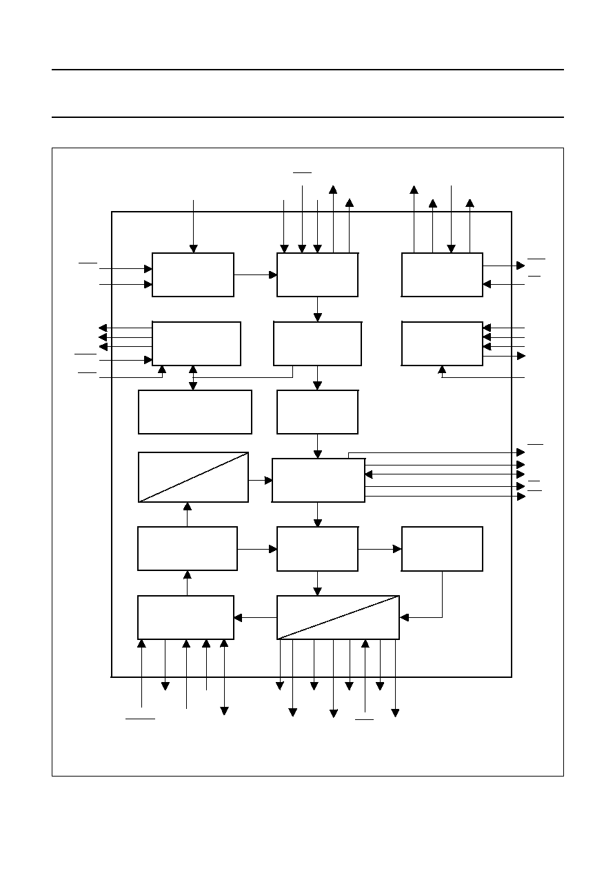
BLOCK DIAGRAM
7
PINNING
8
FUNCTIONAL DESCRIPTION
9
INTERFACE DESCRIPTION
9.1
Input interface
9.2
Memory interface
9.3
Parallel output interface
9.4
Serial output interface
9.5
Simple full capacity output
9.6
RDI output
9.7
Microcontroller interface
9.7.1
I
2
C-bus mode
9.7.2
L3-bus mode
9.7.3
Microcontroller interface registers
10
LIMITING VALUES
11
THERMAL CHARACTERISTICS
12
DC CHARACTERISTICS
13
AC CHARACTERISTICS
14
APPLICATION INFORMATION
14.1
Clock oscillator
14.2
Reset input
14.3
Boundary scan test interface
15
PACKAGE OUTLINE
16
SOLDERING
16.1
Introduction to soldering surface mount
packages
16.2
Reflow soldering
16.3
Wave soldering
16.4
Manual soldering
16.5
Suitability of surface mount IC packages for
wave and reflow soldering methods
17
DATA SHEET STATUS
18
DEFINITIONS
19
DISCLAIMERS
20
PURCHASE OF PHILIPS I
2
C COMPONENTS

2000 Jun 14
3
Philips Semiconductors
Preliminary specification
Digital audio broadcast channel decoder
SAA3500H
1
FEATURES
∑
Digital Audio Broadcast (DAB) full-capacity demodulator
and decoder
∑
Supports DAB transmission modes I, II, III and IV
∑
Integrated Analog-to-Digital Converter (ADC) for
IF input
∑
Digital mixer with on-chip digital Automatic Frequency
Control (AFC) and Automatic Gain Control (AGC)
∑
Detectors for null symbol, DAB mode and transmitter
identification
∑
On-chip or external synchronization algorithms and
control loops
∑
On-chip timing PLL and DCXO
∑
Dynamic DAB multiplex reconfiguration supported
∑
Equal and unequal error protection for up to
64 sub-channels
∑
Fast information channel buffering
∑
Simple full capacity output
∑
Receiver data interface
∑
Serial output for three sub-channels
∑
I
2
C-bus or L3-bus control interface.
2
APPLICATIONS
∑
Mobile receivers (FM/DAB car radios)
∑
Personal Computer add-ons
∑
Test and measurement equipment
∑
Portable radios.
3
GENERAL DESCRIPTION
The Philips SAA3500H is a Digital Audio Broadcast (DAB)
channel decoder according to the ETSI specification
ETS 300 401. The SAA3500H is a successor to the Philips
FADIC and SIVIC chip set and provides an IF ADC, digital
mixer, full DAB ensemble demodulation and decoding as
well as time and frequency synchronization functions.
Because of the full-speed Viterbi decoding capacity and a
high-speed receiver data output interface, DAB data
reception is not limited by the SAA3500H channel
decoder.
4
QUICK REFERENCE DATA
5
ORDERING INFORMATION
SYMBOL
PARAMETER
MIN.
TYP.
MAX.
UNIT
V
DD
supply voltage
3.0
3.3
3.6
V
V
i(max)
maximum input voltage
-
0.5
-
V
DD
+ 0.5
V
I
DD
DC supply current
-
-
180
mA
f
clk
clock frequency
-
24576
-
kHz
T
amb
ambient temperature
-
40
+25
+85
∞
C
T
stg
storage temperature
-
65
-
+150
∞
C
TYPE NUMBER
PACKAGE
NAME
DESCRIPTION
VERSION
SAA3500H
QFP100
plastic quad flat package; 100 leads (lead length 1.95 mm);
body 14
◊
20
◊
2.7 mm; high stand-off height
SOT317-1
2000 Jun 14
5
Philips Semiconductors
Preliminary specification
Digital audio broadcast channel decoder
SAA3500H
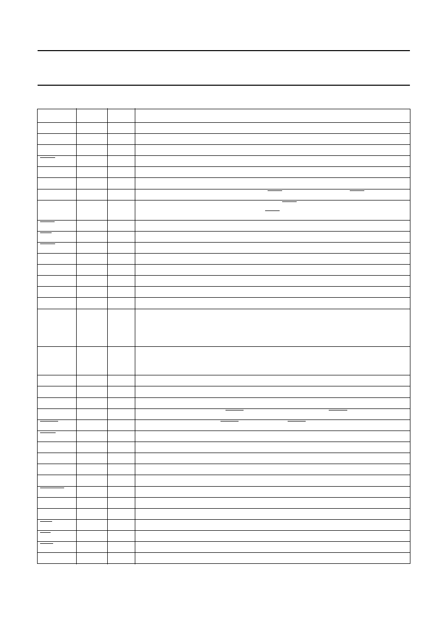
7
PINNING
SYMBOL
PIN
TYPE
DESCRIPTION
ADC
1
input
analog-to-digital converter DC input
AIF
2
input
analog-to-digital converter IF input
V
SSA
3
ground analog supply ground
ADE
99
input
analog-to-digital converter enable (active LOW)
V
DDA
100
supply
analog voltage supply (+3.3 V)
INP[0:9]
8 to 17
input
2048 kHz IF or baseband digital parallel input data (8 or 10 bits)
ADCLK
19
output
analog-to-digital clock output 8192 kHz if BYP = HIGH, 4096 kHz if BYP = LOW
IQS
20
input
clock signal indicating I or Q baseband data if BYP = LOW;
signal for swapping I and Q data bytes if BYP = HIGH
BYP
21
input
IF input stage bypass (active LOW)
FSI
22
input
frame sync input (LOW indicates DAB null symbol detection)
FSO
23
output
null detector/frame sync output (LOW indicates DAB null symbol position)
SLI
24
output
AGC synchronization lock indicator (HIGH if synchronized)
AGC
25
output
AGC level comparator output (HIGH if input sample > reference level, else LOW)
OSCI
4
input
oscillator or system clock input, 24576 kHz
OSCO
5
output
oscillator output
MCLK
41
output
master clock output, 24576 kHz
V
SS
7, 18,
26, 40,
60, 80
and 94
supply
digital supply ground
V
DD
6, 28,
42 and
79
supply
digital voltage supply (+3.3 V)
TEST
92
input
connect to ground for proper operation
OUT[0:7]
32 to 39 output
baseband or channel impulse response output
OCLK
27
output
output data clock (negative edge indicates new data)
OIQ
29
output
output I or Q select signal if OCIR = HIGH, or frame trigger if OCIR = LOW
OCIR
30
input
output select: baseband if OCIR = HIGH, CIR if OCIR = LOW
OEN
31
input
output enable (active LOW)
CFIC
51
output
microcontroller interface signal indicating Fast Information Channel (FIC) processing
CMODE
52
input
microcontroller interface mode input (only L3-bus)
CDATA
53
I/O
microcontroller interface serial data I
2
C-bus or L3-bus (5 V tolerant)
CCLK
54
input
microcontroller interface clock input I
2
C-bus or L3-bus
RESET
55
input
chip reset input (active LOW)
A[17:11]
62 to 68 output
address outputs external RAM
A[10:0]
81 to 91 output
address outputs external RAM
WR
61
output
write data to RAM (active LOW)
RD
69
output
read data from RAM (active LOW)
A17
70
output
address bit 17 inverted for second RAM (128k
◊
8)
D[0:7]
71 to 78 I/O
data input/output external RAM