 | –≠–ª–µ–∫—Ç—Ä–æ–Ω–Ω—ã–π –∫–æ–º–ø–æ–Ω–µ–Ω—Ç: SAA5233P | –°–∫–∞—á–∞—Ç—å:  PDF PDF  ZIP ZIP |
Document Outline
- FEATURES
- GENERAL DESCRIPTION
- QUICK REFERENCE DATA
- ORDERING INFORMATION
- BLOCK DIAGRAM
- PINNING
- LIMITING VALUES
- QUALITY AND RELIABILITY
- CHARACTERISTICS
- FUNCTIONAL DESCRIPTION
- Control of device
- Storage of PDC data
- Error indication
- I 2 C-bus interface
- Register map
- Register 00:Control/Status (reset state XXX0 XX00)
- Register 01: Interrupt (reset state X00X XXXX)
- Register 02 to 0F (HEX): VPS data bytes
- Register 11 to 1D (HEX): Teletext packet 8/30/2 data bytes
- Register 1E to 31D (HEX): Status display message
- I 2 C-bus slave address
- I 2 C-bus increment
- Initialization during power-up
- APPLICATION INFORMATION
- PACKAGE OUTLINES
- SOLDERING
- DEFINITIONS
- LIFE SUPPORT APPLICATIONS
- PURCHASE OF PHILIPS I 2 C COMPONENTS

DATA SHEET
Objective specification
File under Integrated Circuits, IC02
June 1994
INTEGRATED CIRCUITS
Philips Semiconductors
SAA5233
Dual standard PDC decoder
June 1994
2
Philips Semiconductors
Objective specification
Dual standard PDC decoder
SAA5233
FEATURES
∑
Digital data slicer
∑
Acquisition and decoding of VPS data
(EBU PDC System A)
∑
Acquisition and decoding of Teletext packet 8/30/2 data
(EBU PDC System B)
∑
Separate storage of VPS data and packet 8/30/2
allowing dual standard PDC decoders
∑
I
2
C-bus interface with automatic word address
increment
∑
Programmable interrupt for data received
∑
Programmable error level detection
∑
Single +5 V power supply.
GENERAL DESCRIPTION
The SAA5233 is a dual standard Program Delivery Control
(PDC) decoder, allowing the reception and decoding of
both VPS data (EBU PDC System A) and Teletext packet
8/30/2 data (EBU PDC System B). It is intended for use in
European video recorders which are manually
programmed, so that they receive broadcast real time
switching signals for accurate timing of program recording.
QUICK REFERENCE DATA
ORDERING INFORMATION
SYMBOL
PARAMETER
MIN.
TYP.
MAX.
UNIT
V
DD
supply voltage
4.5
5.0
5.5
V
I
DD
supply current
-
30
45
mA
f
clk
crystal input frequency
-
27
-
MHz
V
sync
CVBS sync voltage amplitude
0.1
0.3
0.6
V
V
vid(p-p)
CVBS video voltage amplitude
(peak-to-peak value)
0.7
1.0
1.4
V
T
amb
operating ambient temperature
-
20
-
+70
∞
C
T
stg
storage temperature
-
55
-
+125
∞
C
TYPE NUMBER
PACKAGE
PINS
PIN POSITION
MATERIAL
CODE
SAA5233P
16
DIP16
plastic
SOT38-1
SAA5233T
20
SO20L
plastic
SOT163-1
June 1994
3
Philips Semiconductors
Objective specification
Dual standard PDC decoder
SAA5233
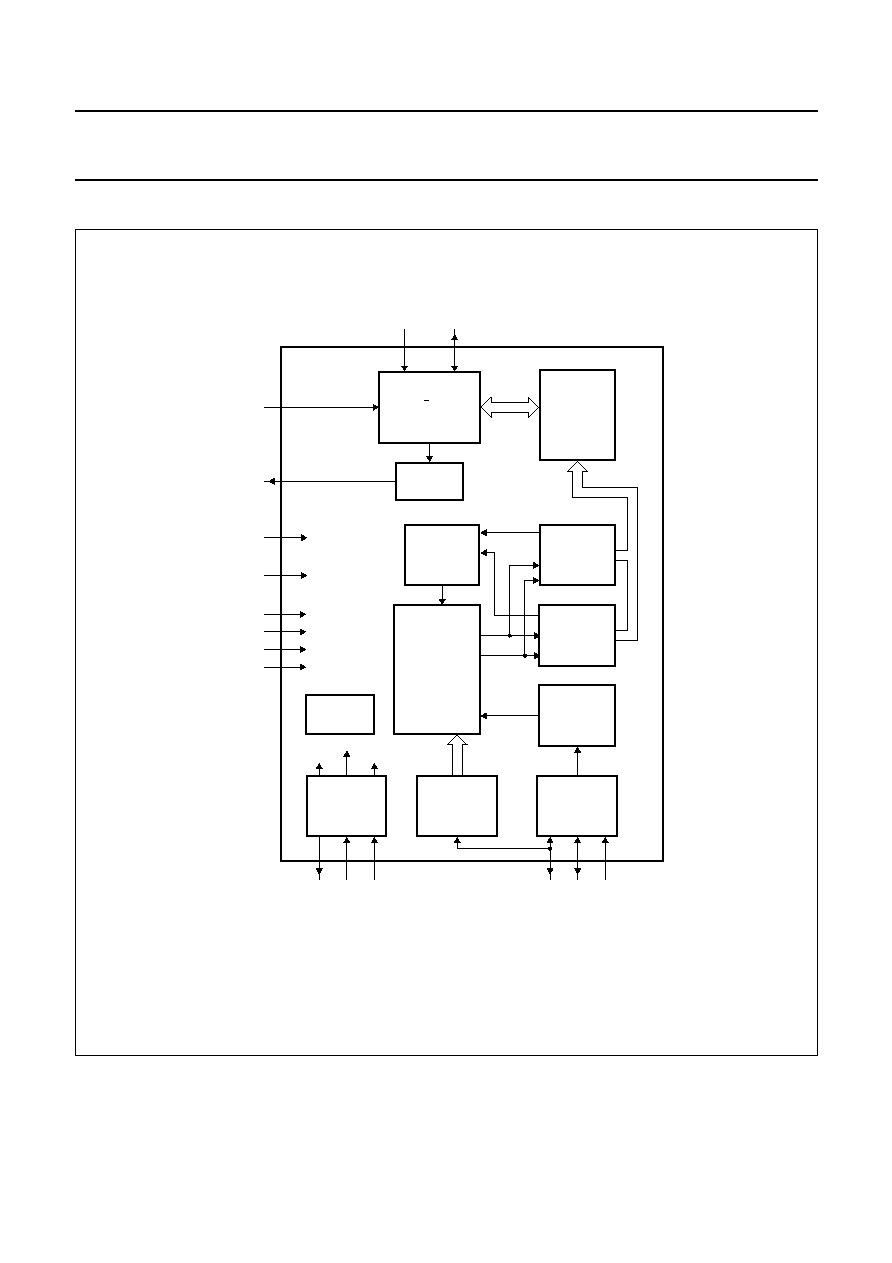
BLOCK DIAGRAM
Fig.1 Block diagram; pin numbers for DIP16.
handbook, full pagewidth
I C BUS
INTERFACE
2
INTERRUPT
CONTROL
MEMORY
INTERFACE
AND RAM
TELETEXT
AND VPS
CONTROL
8/30/2
ACQUISITION
AND
DECODING
DATA SLICER
AND CLOCK
REGENERATOR
VPS
ACQUISITION
AND
DECODING
PLL AND
TIMING
POWER
ON RESET
27 MHz
OSCILLATOR
AND DIVIDER
ANALOGUE
TO DIGITAL
CONVERTER
INPUT
CLAMP
AND SYNC
SEPARATOR
27 MHz
13.5 MHz
1.125 MHz
SCL
SDA
12
13
14
AD
INT
VDD
VSS1
15
4
5
VSS2
9
VSS3
VSS4
VSS5
10
11
16
OSCOUT OSCIN OSCGND
CVBS BLACK IREF
3
2
1
8
7
6
MLB725
SAA5233

June 1994
4
Philips Semiconductors
Objective specification
Dual standard PDC decoder
SAA5233
PINNING
SYMBOL
PIN
DESCRIPTION
DIP16
SO20L
CVBS
1
1
composite video input
BLACK
2
2
video black level storage pin
n.c.
-
3
not connected
IREF
3
4
reference current input
V
DD
4
5
+5 V supply
V
SS1
5
6
0 V ground 1 (main ground pin)
OSCOUT
6
7
27 MHz crystal oscillator output
n.c.
-
8
not connected
OSCIN
7
9
27 MHz crystal oscillator input
OSCGND
8
10
27 MHz crystal oscillator ground
V
SS2
9
11
0 V ground 2; connect to V
SS1
V
SS3
10
12
0 V ground 3; connect to V
SS1
n.c.
-
13
not connected
V
SS4
11
14
connect to V
SS1
in normal operation
SCL
12
15
serial clock open-drain input for I
2
C-bus
SDA
13
16
serial data open-drain input/output for I
2
C-bus
i.c.
-
17
internally connected; do not connect in normal operation
AD
14
18
programmable I
2
C-bus address bit input
INT
15
19
interrupt open-drain output
V
SS5
16
20
connect to V
SS1
in normal operation
Fig.2 Pin configuration; DIP16.
handbook, halfpage
1
2
3
4
5
6
7
8
16
15
14
13
12
11
10
9
SCL
SDA
AD
INT
VDD
VSS1
VSS2
VSS3
VSS4
VSS5
OSCOUT
OSCIN
OSCGND
CVBS
BLACK
IREF
SAA5233
MLB726
Fig.3 Pin configuration; SO20L.
handbook, halfpage
1
2
3
4
5
6
7
8
9
10
20
19
18
17
16
15
14
13
12
11
SCL
SDA
AD
INT
VDD
VSS1
VSS2
VSS3
VSS5
VSS4
OSCOUT
OSCIN
OSCGND
CVBS
BLACK
n.c.
n.c.
n.c.
i.c.
IREF
SAA5233
MLB727
June 1994
5
Philips Semiconductors
Objective specification
Dual standard PDC decoder
SAA5233
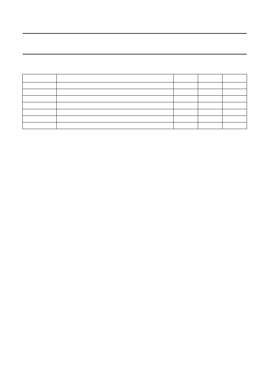
LIMITING VALUES
In accordance with the Absolute Maximum Rating System (IEC 134).
SYMBOL
PARAMETER
MIN.
MAX.
UNIT
V
DD
supply voltage
-
0.3
+6.5
V
V
Imax
maximum input voltage (any input)
-
0.3
V
DD
+ 0.3
V
V
Omax
maximum output voltage (any output)
-
0.3
V
DD
+ 0.3
V
I
IOmax
maximum DC input or output diode current
-
±
20
mA
I
Omax
maximum output current (any output)
-
±
10
mA
T
amb
operating ambient temperature
-
20
+70
∞
C
T
stg
storage temperature
-
55
+125
∞
C