 | –≠–ª–µ–∫—Ç—Ä–æ–Ω–Ω—ã–π –∫–æ–º–ø–æ–Ω–µ–Ω—Ç: SAA5360HL | –°–∫–∞—á–∞—Ç—å:  PDF PDF  ZIP ZIP |

DATA SHEET
Product specification
Supersedes data of 2005 Jan 25
2005 Mar 09
INTEGRATED CIRCUITS
SAA5360; SAA5361
Multi page intelligent teletext
decoder

2005 Mar 09
2
Philips Semiconductors
Product specification
Multi page intelligent teletext decoder
SAA5360; SAA5361
CONTENTS
1
FEATURES
2
GENERAL DESCRIPTION
3
QUICK REFERENCE DATA
4
ORDERING INFORMATION
5
BLOCK DIAGRAM
6
PINNING
6.1
Type SAA5360
6.2
Type SAA5361
7
COMMANDS AND CHARACTER SETS
7.1
High-level command interface
7.2
Character sets
8
LIMITING VALUES
9
THERMAL CHARACTERISTICS
10
QUALITY AND RELIABILITY
11
CHARACTERISTICS
12
APPLICATION INFORMATION
12.1
EMC guidelines
12.2
Application diagram
12.3
Application notes
12.3.1
External data memory access
12.3.2
Symbol explanations
13
PACKAGE OUTLINE
14
SOLDERING
14.1
Introduction to soldering surface mount
packages
14.2
Reflow soldering
14.3
Wave soldering
14.4
Manual soldering
14.5
Suitability of surface mount IC packages for
wave and reflow soldering methods
15
DATA SHEET STATUS
16
DEFINITIONS
17
DISCLAIMERS
18
PURCHASE OF PHILIPS I
2
C COMPONENTS

2005 Mar 09
3
Philips Semiconductors
Product specification
Multi page intelligent teletext decoder
SAA5360; SAA5361
1
FEATURES
∑
Support for 50 or 60 and 100 or 120 Hz and progressive
scan display modes
∑
Complete 625 line teletext decoder in one chip reduces
printed-circuit board area and cost
∑
Automatic detection of transmitted fastext links or
service information (packet 8/30)
∑
On-Screen Display (OSD) for user interface menus
using teletext and dedicated menu icons
∑
Video Programming System (VPS) decoding
∑
Wide Screen Signalling (WSS) decoding
∑
SAA5360 supports Pan-European, Arabic and Iranian
character sets
∑
SAA5361 supports Pan-European, Cyrillic, Greek and
Arabic character sets
∑
High-level command interface via I
2
C-bus gives easy
control with a low software overhead
∑
High-level command interface is backward compatible
to Stand-Alone Fastext And Remote Interface (SAFARI)
∑
625 and 525 line display
∑
RGB interface to standard colour decoder ICs; current
source
∑
Versatile 8-bit open-drain Input/Output (I/O) expander;
5 V tolerant
∑
Single 12 MHz crystal oscillator
∑
Single power supply: from 3.0 V to 3.6 V
∑
Operating temperature:
-
20 to +70
∞
C
∑
Automatic detection of transmitted pages to be selected
by page up and page down
∑
8 page fastext decoder
∑
Table Of Pages (TOP) decoder with Basic Top Table
(BTT) and Additional Information Tables (AITs)
∑
4 page user-defined list mode.
2
GENERAL DESCRIPTION
The SAA5360; SAA5361 is a single-chip multi page 625
line world system teletext decoder with a high-level
command interface, and is SAFARI compatible.
The device is designed to minimize the overall system
cost, due to the high-level command interface offering the
benefit of a low software overhead in the TV
microcontroller.
The SAA5360 incorporates the following functions:
∑
10 page teletext decoder with OSD, fastext, TOP,
default and list acquisition modes
∑
Automatic channel installation support.
The functionality of the SAA5361 is similar to the
SAA5360, but offers the capability to store up to
250 additional pages of teletext in an external SRAM.
3
QUICK REFERENCE DATA
Note
1. Periphery supply current is dependent on external components and I/O voltage levels.
SYMBOL
PARAMETER
CONDITIONS
MIN.
TYP.
MAX.
UNIT
V
DD
all supply voltages
referenced to V
SS
3.0
3.3
3.6
V
I
DDP
periphery supply current
note 1
1
-
-
mA
I
DDC
core supply current
normal mode
-
15
18
mA
idle mode
-
4.6
6
mA
I
DDA
analog supply current
normal mode
-
45
48
mA
idle mode
-
0.87
1
mA
f
xtal(nom)
nominal crystal frequency
fundamental mode
-
12
-
MHz
T
amb
ambient temperature
-
20
-
+70
∞
C
T
stg
storage temperature
-
55
-
+125
∞
C

2005 Mar 09
4
Philips Semiconductors
Product specification
Multi page intelligent teletext decoder
SAA5360; SAA5361
4
ORDERING INFORMATION
5
BLOCK DIAGRAM
TYPE NUMBER
PACKAGE
NAME
DESCRIPTION
VERSION
SAA5360HL
LQFP100
plastic low profile quad flat package; 100 leads; body 14
◊
14
◊
1.4 mm
SOT407-1
SAA5361HL
LQFP100
plastic low profile quad flat package; 100 leads; body 14
◊
14
◊
1.4 mm
SOT407-1
mhc633
MICROCONTROLLER
(80C51)
SRAM
256-byte
ROM
(128 or 192-kbyte)
MEMORY
INTERFACE
DISPLAY
R
G
B
VDS
HSYNC
VSYNC
CVBS
DATA
CAPTURE
DRAM
(14-kbyte)
TV CONTROL
AND
INTERFACE
I
2
C-bus,
general I/O
DISPLAY
TIMING
CVBS
DATA
CAPTURE
TIMING
SAA5360
SAA5361
Fig.1 Block diagram.

2005 Mar 09
5
Philips Semiconductors
Product specification
Multi page intelligent teletext decoder
SAA5360; SAA5361
6
PINNING
6.1
Type SAA5360
SYMBOL
PIN
TYPE
DESCRIPTION
P2_7/PWM6
1
I/O
programmable bidirectional port 2: bit 7 or output bit 6 of the 7-bit PWM
P3_0/ADC0
2
I/O
programmable bidirectional port 3: bit 0 or input 0 for the software ADC facility
n.c.
3
-
not connected
P3_1/ADC1
4
I/O
programmable bidirectional port 3: bit 1 or input 1 for the software ADC facility
P3_2/ADC2
5
I/O
programmable bidirectional port 3: bit 2 or input 2 for the software ADC facility
P3_3/ADC3
6
I/O
programmable bidirectional port 3: bit 3 or input 3 for the software ADC facility
n.c.
7
-
not connected
n.c.
8
-
not connected
n.c.
9
-
not connected
n.c.
10
-
not connected
V
SSC
11
-
core ground
V
SSP
12
-
periphery ground
P0_5
13
I/O
8 mA current sinking output for direct drive of LED
n.c.
14
-
not connected
n.c.
15
-
not connected
SCL_NVRAM
16
I
I
2
C-bus serial clock input to non-volatile RAM
SDA_NVRAM
17
I/O
I
2
C-bus serial data input and output of non-volatile RAM
P0_2
18
I/O
programmable bidirectional port 0: bit 2
n.c.
19
-
not connected
n.c.
20
-
not connected
VPE
21
I
OTP programming voltage input; connect to ground
P0_3
22
I/O
programmable bidirectional port 0: bit 3
n.c.
23
-
not connected
P0_4
24
I/O
programmable bidirectional port 0: bit 4
n.c.
25
-
not connected
n.c.
26
-
not connected
n.c.
27
-
not connected
P0_6
28
I/O
8 mA current sinking output for direct drive of LED
P0_7
29
I/O
programmable bidirectional port 0: bit 7
V
SSA
30
-
analog ground
CVBS0
31
I
composite video input 0 selectable via SFR; a positive-going 1 V (p-p) input is
required and connected via a 100 nF capacitor
CVBS1
32
I
composite video input 1 selectable via SFR; a positive-going 1 V (p-p) input is
required and connected via a 100 nF capacitor
n.c.
33
-
not connected
SYNC_FILTER
34
I/O
CVBS sync filter input; this pin should be connected to V
SSA
via a 100 nF
capacitor
IREF
35
I
reference current input for analog circuits and connected to V
SSA
via a 24 k
resistor

2005 Mar 09
6
Philips Semiconductors
Product specification
Multi page intelligent teletext decoder
SAA5360; SAA5361
n.c.
36
-
not connected
n.c.
37
-
not connected
n.c.
38
-
not connected
n.c.
39
-
not connected
n.c.
40
-
not connected
FRAME
41
O
de-interlace output synchronized with the VSYNC pulse to produce a
non-interlaced display by adjustment of the vertical deflection circuits
VPE
42
I
OTP programming voltage input; connect to ground
COR
43
O
output which allows selective contrast reduction of the TV picture to enhance a
mixed mode display; open-drain; active LOW
n.c.
44
-
not connected
V
DDA
45
-
3.3 V analog supply voltage
B
46
O
pixel rate output of the blue colour information
G
47
O
pixel rate output of the green colour information
R
48
O
pixel rate output of the red colour information
n.c.
49
-
not connected
n.c.
50
-
not connected
n.c.
51
-
not connected
VDS
52
O
video or data switch push-pull output for dot rate fast blanking
HSYNC
53
I
Schmitt-triggered input for a TTL-level version of the horizontal sync pulse; the
polarity of this pulse is programmable by register bit TXT1.H POLARITY
n.c.
54
-
not connected
VSYNC
55
I
Schmitt-triggered input for a TTL-level version of the vertical sync pulse; the
polarity of this pulse is programmable by register bit TXT1.V POLARITY
n.c.
56
-
not connected
n.c.
57
-
not connected
n.c.
58
-
not connected
n.c.
59
-
not connected
V
SSP
60
-
periphery ground
n.c.
61
-
not connected
V
SSC
62
-
core ground
V
DDC
63
-
3.3 V core supply voltage
n.c.
64
-
not connected
n.c.
65
-
not connected
n.c.
66
-
not connected
n.c.
67
-
not connected
n.c.
68
-
not connected
OSCGND
69
-
crystal oscillator ground
XTALIN
70
I
12 MHz crystal oscillator input
XTALOUT
71
O
12 MHz crystal oscillator output
RESET
72
I
reset input; if LOW for at least 24 crystal oscillator periods while the oscillator is
running, the device is reset; internal pull-up
SYMBOL
PIN
TYPE
DESCRIPTION

2005 Mar 09
7
Philips Semiconductors
Product specification
Multi page intelligent teletext decoder
SAA5360; SAA5361
RESET
73
I
reset input; if HIGH for at least 24 crystal oscillator periods while the oscillator is
running, the device is reset; this pin should be connected to V
DDC
via a capacitor if
an active HIGH reset is required; internal pull-down
n.c.
74
-
not connected
V
DDP
75
-
3.3 V periphery supply voltage
P1_0
76
I/O
programmable bidirectional port 1: bit 0
n.c.
77
-
not connected
P1_1
78
I/O
programmable bidirectional port 1: bit 1
P1_2
79
I/O
programmable bidirectional port 1: bit 2
P1_3
80
I/O
programmable bidirectional port 1: bit 3
SCL
81
I
I
2
C-bus serial clock input from application
SDA
82
I/O
I
2
C-bus serial data input from or output to application
P1_4
83
I/O
programmable bidirectional port 1: bit 4
P1_5
84
I/O
programmable bidirectional port 1: bit 5
n.c.
85
-
not connected
n.c.
86
-
not connected
n.c.
87
-
not connected
n.c.
88
-
not connected
n.c.
89
-
not connected
n.c.
90
-
not connected
n.c.
91
-
not connected
n.c.
92
-
not connected
P2_1/PWM0
93
I/O
programmable bidirectional port 2: bit 1 or output bit 0 of the 7-bit PWM
P2_2/PWM1
94
I/O
programmable bidirectional port 2: bit 2 or output bit 1 of the 7-bit PWM
P2_3/PWM2
95
I/O
programmable bidirectional port 2: bit 3 or output bit 2 of the 7-bit PWM
P2_4/PWM3
96
I/O
programmable bidirectional port 2: bit 4 or output bit 3 of the 7-bit PWM
P2_5/PWM4
97
I/O
programmable bidirectional port 2: bit 5 or output bit 4 of the 7-bit PWM
P2_6/PWM5
98
I/O
programmable bidirectional port 2: bit 6 or output bit 5 of the 7-bit PWM
V
SSC
99
-
core ground
P2_0/TPWM
100
I/O
programmable bidirectional port 2: bit 0 or output for 14-bit high precision PWM
SYMBOL
PIN
TYPE
DESCRIPTION

2005 Mar 09
8
Philips Semiconductors
Product specification
Multi page intelligent teletext decoder
SAA5360; SAA5361
SAA5360HL
mhc508
1
2
3
4
5
6
7
8
9
10
11
12
13
14
20
21
22
23
24
25
75
74
73
72
71
70
69
68
67
66
65
64
63
62
56
55
54
53
52
51
15
16
17
18
19
61
60
59
58
57
26
27
28
29
30
31
32
33
34
35
36
37
38
39
45
46
47
48
49
50
10
0
99
98
97
96
95
94
93
92
91
90
89
88
87
81
80
79
78
77
76
40
41
42
43
44
86
85
84
83
82
n.c.
P0_4
n.c.
P0_3
VPE
n.c.
n.c.
P0_2
SDA_NVRAM
SCL_NVRAM
n.c.
n.c.
P0_5
V
SSP
V
SSC
n.c.
n.c.
n.c.
n.c.
P3_3/ADC3
P3_2/ADC2
P3_1/ADC1
n.c.
P3_0/ADC0
P2_7/PWM6
n.c.
n.c.
P0
_
6
P0
_
7
V
SSA
CVBS0
CVBS1
n.c.
SYNC_FILTER
IREF
n.c.
n.c.
n.c.
n.c.
n.c.
FRAME
VPE
COR
n.c.
V
DDA
B
G
R
n.c.
n.c.
n.c.
VDS
HSYNC
n.c.
VSYNC
n.c.
n.c.
n.c.
n.c.
V
SSP
n.c.
V
SSC
V
DDC
n.c.
n.c.
n.c.
n.c.
n.c.
OSCGND
XTALIN
XTALOUT
RESET
RESET
n.c.
V
DDP
P2
_
0
/
TPWM
V
SSC
P2
_
6
/
PWM5
P2
_
5
/
PWM4
P2
_
4
/
PWM3
P2
_
3
/
PWM2
P2
_
2
/
PWM1
P2
_
1
/
PWM0
n.c.
n.c.
n.c.
n.c.
n.c.
n.c.
n.c.
n.c.
P1
_
5
P1
_
4
SDA
SCL
P1
_
3
P1
_
2
P1
_
1
n.c.
P1
_
0
Fig.2 Pin configuration of SAA5360HL.

2005 Mar 09
9
Philips Semiconductors
Product specification
Multi page intelligent teletext decoder
SAA5360; SAA5361
6.2
Type SAA5361
SYMBOL
PIN
TYPE
DESCRIPTION
P2_7/PWM6
1
I/O
programmable bidirectional port 2: bit 7 or output bit 6 of the 6-bit PWM
P3_0/ADC0
2
I/O
programmable bidirectional port 3 with alternative functions: bit 0 or input 0 for the
software ADC facility
n.c.
3
O
not connected
P3_1/ADC1
4
I/O
programmable bidirectional port 3 with alternative functions: bit 1 or input 1 for the
software ADC facility
P3_2/ADC2
5
I/O
programmable bidirectional port 3 with alternative functions: bit 2 or input 2 for the
software ADC facility
P3_3/ADC3
6
I/O
programmable bidirectional port 3 with alternative functions: bit 3 or input 3 for the
software ADC facility
n.c.
7
O
not connected
A14
8
O
address line 14
RD
9
O
read control output to external data memory; active LOW
WR
10
O
write control output to external data memory; active LOW
V
SSC
11
-
core ground
V
SSP
12
-
periphery ground
P0_5
13
I/O
8 mA current sinking output for direct drive of LED
n.c.
14
I
not connected
A7
15
O
address line 7
SCL_NVRAM
16
I
I
2
C-bus serial clock input to non-volatile RAM
SDA_NVRAM
17
I/O
I
2
C-bus serial data input and output of non-volatile RAM
P0_2
18
I/O
programmable bidirectional port 0 with alternative functions: bit 2 input and output
for general use
n.c.
19
O
not connected
n.c.
20
O
not connected
VPE
21
I
OTP programming voltage input; connect to ground
P0_3
22
I/O
programmable bidirectional port 0 with alternative functions: bit 3 input and output
for general use
A6
23
O
address line 6
P0_4
24
I/O
programmable bidirectional port 0 with alternative functions: bit 4 input and output
for general use
n.c.
25
I/O
not connected
A5
26
O
address line 5
A4
27
O
address line 4
P0_6
28
I/O
8 mA current sinking output for direct drive of LED
P0_7
29
I/O
programmable bidirectional port 0 with alternative functions: bit 7 input and output
for general use
V
SSA
30
-
analog ground
CVBS0
31
I
composite video input 0 selectable via SFR; a positive-going 1 V (p-p) input is
required and connected via a 100 nF capacitor
CVBS1
32
I
composite video input 1 selectable via SFR; a positive-going 1 V (p-p) input is
required and connected via a 100 nF capacitor

2005 Mar 09
10
Philips Semiconductors
Product specification
Multi page intelligent teletext decoder
SAA5360; SAA5361
A15_BK
33
O
address line 15
SYNC_FILTER
34
I/O
CVBS sync filter input; this pin should be connected to V
SSA
via a 100 nF capacitor
IREF
35
I
reference current input for analog circuits and connected to V
SSA
via a 24 k
resistor
A13
36
O
address line 13
A12
37
O
address line 12
A3
38
O
address line 3
A2
39
O
address line 2
A1
40
O
address line 1
FRAME
41
O
de-interlace output synchronized with the VSYNC pulse to produce a
non-interlaced display by adjustment of the vertical deflection circuits
VPE
42
I
OTP programming voltage input; connect to ground
COR
43
O
output which allows selective contrast reduction of the TV picture to enhance a
mixed mode display; open-drain; active LOW
n.c.
44
I/O
not connected
V
DDA
45
-
3.3 V analog supply voltage
B
46
O
pixel rate output of the blue colour information
G
47
O
pixel rate output of the green colour information
R
48
O
pixel rate output of the red colour information
A0
49
O
address line 0
RAMBK1
50
O
RAMBK SFR selection bits input 1 for external program SRAM data storage
RAMBK0
51
O
RAMBK SFR selection bits input 0 for external program SRAM data storage
VDS
52
O
video or data switch push-pull output for dot rate fast blanking
HSYNC
53
I
Schmitt-triggered input for a TTL-level version of the horizontal sync pulse; the
polarity of this pulse is programmable by register bit TXT1.H POLARITY
n.c.
54
I/O
not connected
VSYNC
55
I
Schmitt-triggered input for a TTL-level version of the vertical sync pulse; the polarity
of this pulse is programmable by register bit TXT1.V POLARITY
n.c.
56
O
not connected
n.c.
57
O
not connected
n.c.
58
O
not connected
n.c.
59
I/O
not connected
V
SSP
60
-
periphery ground
n.c.
61
I
not connected (internal pull-up)
V
SSC
62
-
core ground
V
DDC
63
-
3.3 V core supply voltage
A11
64
O
address line 11
A10
65
O
address line 10
A9
66
O
address line 9
A8
67
O
address line 8
n.c.
68
O
not connected
OSCGND
69
-
crystal oscillator ground
SYMBOL
PIN
TYPE
DESCRIPTION

2005 Mar 09
11
Philips Semiconductors
Product specification
Multi page intelligent teletext decoder
SAA5360; SAA5361
XTALIN
70
I
12 MHz crystal oscillator input
XTALOUT
71
O
12 MHz crystal oscillator output
RESET
72
I
reset input; if LOW for at least 24 crystal oscillator periods while the oscillator is
running, the device is reset; internal pull-up
RESET
73
I
reset input; if HIGH for at least 24 crystal oscillator periods while the oscillator is
running, the device is reset; this pin should be connected to V
DDC
via a capacitor if
an active HIGH reset is required; internal pull-down
n.c.
74
O
not connected
V
DDP
75
-
3.3 V periphery supply voltage
P1_0
76
IO
programmable bidirectional port 1 with alternative functions: bit 0 input and output
for general use
n.c.
77
O
not connected
P1_1
78
I/O
programmable bidirectional port 1 with alternative functions: bit 1 input and output
for general use
P1_2
79
I/O
programmable bidirectional port 1 with alternative functions: bit 2 input and output
for general use
P1_3
80
I/O
programmable bidirectional port 1 with alternative functions: bit 3 input and output
for general use
SCL
81
I
I
2
C-bus serial clock input from application
SDA
82
I/O
I
2
C-bus serial data input from or output to application
P1_4
83
I/O
programmable bidirectional port 1 with alternative functions: bit 4 input and output
for general use
P1_5
84
I/O
programmable bidirectional port 1 with alternative functions: bit 5 input and output
for general use
AD0
85
I/O
address line 0 with multiplexed data line 0
AD1
86
I/O
address line 1 with multiplexed data line 1
AD2
87
I/O
address line 2 with multiplexed data line 2
AD3
88
I/O
address line 3 with multiplexed data line 3
AD4
89
I/O
address line 4 with multiplexed data line 4
AD5
90
I/O
address line 5 with multiplexed data line 5
AD6
91
I/O
address line 6 with multiplexed data line 6
AD7
92
I/O
address line 7 with multiplexed data line 7
P2_1/PWM0
93
I/O
programmable bidirectional port 2: bit 1 or output bit 0 of the 6-bit PWM
P2_2/PWM1
94
I/O
programmable bidirectional port 2: bit 2 or output bit 1 of the 6-bit PWM
P2_3/PWM2
95
I/O
programmable bidirectional port 2: bit 3 or output bit 2 of the 6-bit PWM
P2_4/PWM3
96
I/O
programmable bidirectional port 2: bit 4 or output bit 3 of the 6-bit PWM
P2_5/PWM4
97
I/O
programmable bidirectional port 2: bit 5 or output bit 4 of the 6-bit PWM
P2_6/PWM5
98
I/O
programmable bidirectional port 2: bit 6 or output bit 5 of the 6-bit PWM
V
SSC
99
-
core ground
P2_0/TPWM
100
I/O
programmable bidirectional port 2: bit 0 or output for 14-bit high precision PWM
SYMBOL
PIN
TYPE
DESCRIPTION

2005 Mar 09
12
Philips Semiconductors
Product specification
Multi page intelligent teletext decoder
SAA5360; SAA5361
SAA5361HL
001aaa526
1
2
3
4
5
6
7
8
9
10
11
12
13
14
20
21
22
23
24
25
75
74
73
72
71
70
69
68
67
66
65
64
63
62
56
55
54
53
52
51
15
16
17
18
19
61
60
59
58
57
26
27
28
29
30
31
32
33
34
35
36
37
38
39
45
46
47
48
49
50
10
0
99
98
97
96
95
94
93
92
91
90
89
88
87
81
80
79
78
77
76
40
41
42
43
44
86
85
84
83
82
n.c.
P0_4
A6
P0_3
VPE
n.c.
n.c.
P0_2
SDA_NVRAM
SCL_NVRAM
A7
n.c.
P0_5
V
SSP
V
SSC
RD
WR
A14
n.c.
P3_3/ADC3
P3_2/ADC2
P3_1/ADC1
n.c.
P3_0/ADC0
P2_7/PWM6
A5
A4
P0
_
6
P0
_
7
V
SSA
CVBS0
CVBS1
A15_BK
SYNC_FILTER
IREF
A13
A12
A3
A2
A1
FRAME
VPE
COR
n.c.
V
DDA
B
G
R
A0
RAMBK1
RAMBK0
VDS
HSYNC
n.c.
VSYNC
n.c.
n.c.
n.c.
n.c.
V
SSP
n.c.
V
SSC
V
DDC
A11
A10
A9
A8
n.c.
OSCGND
XTALIN
XTALOUT
RESET
RESET
n.c.
V
DDP
P2
_
0
/
TPWM
V
SSC
P2
_
6
/
PWM5
P2
_
5
/
PWM4
P2
_
4
/
PWM3
P2
_
3
/
PWM2
P2
_
2
/
PWM1
P2
_
1
/
PWM0
AD7
AD6
AD5
AD4
AD3
AD2
AD1
AD0
P1
_
5
P1
_
4
SDA
SCL
P1
_
3
P1
_
2
P1
_
1
n.c.
P1
_
0
Fig.3 Pin configuration of SAA5361HL.

2005 Mar 09
13
Philips Semiconductors
Product specification
Multi page intelligent teletext decoder
SAA5360; SAA5361
7
COMMANDS AND CHARACTER SETS
7.1
High-level command interface
The I
2
C-bus interface is used to pass control commands and data between the SAA5360; SAA5361 and the television
microcontroller. The interface uses high-level commands, which are backwards compatible with the SAFARI.
The I
2
C-bus transmission formats are given in Tables 1 to 3.
Table 1
User command
Table 2
System command
Table 3
User read
7.2
Character sets
The SAA5360HL/M1/0004 contains the character set for Pan-Euro, Arabic and Iranian and has slave address 58H.
The SAA5361HL/M1/1651 contains the character set for Pan-Euro, Cyrillic, Greek and Arabic and has slave address
60H.
USER COMMAND
START
I
2
C-bus address
write
ACK
command
ACK
STOP
SYSTEM COMMAND
START
I
2
C-bus address
write
ACK
command
ACK
parameter
ACK
STOP
USER READ
START
I
2
C-bus address
read
ACK
data
ACK
STOP

2005 Mar 09
14
Philips Semiconductors
Product specification
Multi page intelligent teletext decoder
SAA5360; SAA5361
8
LIMITING VALUES
In accordance with Absolute Maximum Rating System (IEC 60134).
Note
1. This maximum value refers to 5 V tolerant I/Os and may be 6 V maximum but only when V
DD
is present.
9
THERMAL CHARACTERISTICS
10 QUALITY AND RELIABILITY
In accordance with
"General Quality Specification for Integrated circuits SNW-FQ-611".
SYMBOL
PARAMETER
CONDITIONS
MIN.
MAX.
UNIT
V
DD
all supply voltages
-
0.5
+4.0
V
V
I
input voltage (any input)
V
DD
< 3.6 V; note 1
-
0.5
V
DD
+ 0.5
V
V
DD
3.6 V; note 1
-
0.5
4.1
V
V
O
output voltage (any output)
note 1
-
0.5
V
DD
+ 0.5
V
I
O
output current (each output)
-
10
mA
I
IO(d)
diode DC input or output current
-
20
mA
T
amb
ambient temperature
-
20
+70
∞
C
T
j
junction temperature
-
20
+125
∞
C
T
stg
storage temperature
-
55
+125
∞
C
V
esd
electrostatic discharge voltage
Human body model;
C = 100 pF; R = 1.5 k
-
2000
V
Machine model;
C = 200 pF; R = 0
-
200
V
I
lu
latch-up current
1.5
◊
V
DD
-
100
mA
SYMBOL
PARAMETER
CONDITIONS
VALUE
UNIT
R
th(j-a)
thermal resistance from junction to ambient
in free air
52
K/W
R
th(j-c)
thermal resistance from junction to case
8
K/W

2005 Mar 09
15
Philips Semiconductors
Product specification
Multi page intelligent teletext decoder
SAA5360; SAA5361
11 CHARACTERISTICS
V
DD
= 3.3 V
±
10 %; V
SS
= 0 V; T
amb
=
-
20
∞
C to +70
∞
C; unless otherwise specified.
SYMBOL
PARAMETER
CONDITIONS
MIN.
TYP.
MAX.
UNIT
Supplies
V
DD
any supply voltage
referenced to V
SS
3.0
3.3
3.6
V
I
DDP
periphery supply current
note 1
1
-
-
mA
I
DDC
core supply current
operating mode
-
15
18
mA
idle mode
-
4.6
6
mA
power-down mode
-
0.76
1
mA
I
DDA
analog supply current
operating mode
-
45
48
mA
idle mode
-
0.87
1
mA
power-down mode
-
0.45
0.7
mA
Digital inputs
P
IN
RESET
V
IL
LOW-level input voltage
-
-
1.00
V
V
IH
HIGH-level input voltage
1.85
-
5.5
V
V
hys
hysteresis voltage of Schmitt-trigger input
0.44
-
0.58
V
I
LI
input leakage current
V
I
= 0
-
-
0.17
µ
A
R
pd
equivalent pull-down resistance
V
I
= V
DD
55.73 70.71
92.45
k
P
IN
RESET
V
IL
LOW-level input voltage
-
-
0.98
V
V
IH
HIGH-level input voltage
1.73
-
5.5
V
V
hys
hysteresis voltage of Schmitt-trigger input
0.41
-
0.5
V
I
LI
input leakage current
V
I
= V
DD
-
-
0.00
µ
A
R
pu
equivalent pull-up resistance
V
I
= 0
46.07 55.94
70.01
k
P
INS
HSYNC
AND
VSYNC
V
IL
LOW-level input voltage
-
-
0.96
V
V
IH
HIGH-level input voltage
1.80
-
5.5
V
V
hys
hysteresis of Schmitt-trigger input
0.40
-
0.56
V
I
LI
input leakage current
V
I
= 0 to V
DD
-
-
0.00
µ
A
Digital outputs
P
INS
FRAME
AND
VDS
V
OL
LOW-level output voltage
I
OL
= 3 mA
-
-
0.13
V
V
OH
HIGH-level output voltage
I
OH
= 3 mA
2.84
-
-
V
t
o(r)
output rise time
10 % to 90 % of V
DD
;
C
L
= 70 pF
7.50
8.85
10.90
ns
t
o(f)
output fall time
10 % to 90 % of V
DD
;
C
L
= 70 pF
6.70
7.97
10.00
ns

2005 Mar 09
16
Philips Semiconductors
Product specification
Multi page intelligent teletext decoder
SAA5360; SAA5361
P
IN
COR (
OPEN
-
DRAIN
)
V
OL
LOW-level output voltage
I
OL
= 3 mA
-
-
0.14
V
V
OH
HIGH-level pull-up output voltage
I
OL
=
-
3 mA; push-pull
2.84
-
-
V
I
LI
input leakage current
V
I
= 0 to V
DD
-
-
0.12
µ
A
t
o(r)
output rise time
10 % to 90 % of V
DD
;
C
L
= 70 pF
7.20
8.64
11.10
ns
t
o(f)
output fall time
10 % to 90 % of V
DD
;
C
L
= 70 pF
4.90
7.34
9.40
ns
Digital input/outputs
P
INS
SCL_NVRAM, SDA_NVRAM, P0_4
TO
P0_7, P1_0, P1_1, P2_1
TO
P2_7
AND
P3_0
TO
P3_4
V
IL
LOW-level input voltage
-
-
0.98
V
V
IH
HIGH-level input voltage
1.78
-
5.50
V
V
hys
hysteresis of Schmitt-trigger input
0.41
-
0.55
V
I
LI
input leakage current
V
I
= 0 to V
DD
-
-
0.01
µ
A
V
OL
LOW-level output voltage
I
OL
= 4 mA
-
-
0.18
V
V
OH
HIGH-level output voltage
I
OH
=
-
4 mA; push-pull
2.81
-
-
V
t
o(r)
output rise time
10 % to 90 % of V
DD
;
C
L
= 70 pF; push-pull
6.50
8.47
10.70
ns
t
o(f)
output fall time
10 % to 90 % of V
DD
;
C
L
= 70 pF
5.70
7.56
10.00
ns
P
INS
P1_2, P1_3
AND
P2_0
V
IL
LOW-level input voltage
-
-
0.99
V
V
IH
HIGH-level input voltage
1.80
-
5.50
V
V
hys
hysteresis voltage of Schmitt-trigger input
0.42
-
0.56
V
I
LI
input leakage current
V
I
= 0 to V
DD
-
-
0.02
µ
A
V
OL
LOW-level output voltage
I
OL
= 4 mA
-
-
0.17
V
V
OH
HIGH-level output voltage
I
OH
=
-
4 mA; push-pull
2.81
-
-
V
t
o(r)
output rise time
10 % to 90 % of V
DD
;
C
L
= 70 pF; push-pull
7.00
8.47
10.50
ns
t
o(f)
output fall time
10 % to 90 % of V
DD
;
C
L
= 70 pF
5.40
7.36
9.30
ns
P
INS
P0_5
AND
P0_6
V
IL
LOW-level input voltage
-
-
0.98
V
V
IH
HIGH-level input voltage
1.82
-
5.50
V
I
LI
input leakage current
V
I
= 0 to V
DD
-
-
0.11
µ
A
V
hys
hysteresis voltage of Schmitt-trigger input
0.42
-
0.58
V
V
OL
LOW-level output voltage
I
OL
= 8 mA
-
-
0.20
V
V
OH
HIGH-level output voltage
I
OH
=
-
8 mA; push-pull
2.76
-
-
V
t
o(r)
output rise time
10 % to 90 % of V
DD
;
C
L
= 70 pF; push-pull
7.40
8.22
8.80
ns
SYMBOL
PARAMETER
CONDITIONS
MIN.
TYP.
MAX.
UNIT

2005 Mar 09
17
Philips Semiconductors
Product specification
Multi page intelligent teletext decoder
SAA5360; SAA5361
t
o(f)
output fall time
10 % to 90 % of V
DD
;
C
L
= 70 pF
4.20
4.57
5.20
ns
P
INS
P1_4
AND
P1_5 (
OPEN DRAIN
)
V
IL
LOW-level input voltage
-
-
1.08
V
V
IH
HIGH-level input voltage
1.99
-
5.50
V
V
hys
hysteresis voltage of Schmitt-trigger input
0.49
-
0.60
V
I
LI
input leakage current
V
I
= 0 to V
DD
-
-
0.13
µ
A
V
OL
LOW-level output voltage
I
OL
= 8 mA
-
-
0.35
V
t
o(f)
output fall time
10 % to 90 % of V
DD
;
C
L
= 70 pF
69.70 83.67
103.30
ns
t
o(f)(I2C)
output fall time in relation to the I
2
C-bus
specifications
V
o
= 3 V to 1.5 V at
I
OL
= 3 mA; C
L
= 400 nF
-
57.80
-
ns
Analog inputs
P
INS
CVBS0
AND
CVBS1
V
sync
sync voltage amplitude
0.1
0.3
0.6
V
V
v(p-p)
video input voltage amplitude
(peak-to-peak value)
0.7
1.0
1.4
V
Z
source
source impedance
0
-
250
V
IH
HIGH-level input voltage
3.0
-
V
DDA
+ 0.3
V
C
i
input capacitance
-
-
10
pF
P
IN
IREF
R
gnd
resistance to ground
resistor tolerance 2 %
-
24
-
k
P
INS
ADC0
TO
ADC3
V
IH
HIGH-level input voltage
range = V
DDP
-
V
TN
;
note 2
-
-
V
DDA
V
C
i
input capacitance
-
-
10
pF
Analog outputs
P
INS
R, G
AND
B
I
o(b)
output current (black level)
V
DDA
= 3.3 V
-
10
-
+10
µ
A
I
o(max)
output current (maximum Intensity)
V
DDA
= 3.3 V; intensity
level code = 31 decimal
6.0
6.67
7.3
mA
I
o(70)
output current (70 % of full intensity)
V
DDA
= 3.3 V; intensity
level code = 0 decimal
4.2
4.7
5.1
mA
R
L
load resistor
referenced to V
SSA;
resistor tolerance 5 %
-
150
-
C
L
load capacitance
-
-
15
pF
t
o(r)
output rise time
10 % to 90 % full
intensity
-
16.1
-
ns
t
o(f)
output fall time
90 % to 10 % full
intensity
-
14.5
-
ns
SYMBOL
PARAMETER
CONDITIONS
MIN.
TYP.
MAX.
UNIT

2005 Mar 09
18
Philips Semiconductors
Product specification
Multi page intelligent teletext decoder
SAA5360; SAA5361
Analog input/output
P
IN
SYNC_FILTER
C
sync
storage capacitor to ground
-
100
-
nF
V
sync
sync filter level voltage for nominal sync
amplitude
0.35
0.55
0.75
V
Crystal oscillator
I
NPUT
:
PIN
XTALIN
V
IL
LOW-level input voltage
V
SSA
-
-
V
V
IH
HIGH-level input voltage
-
-
V
DDA
V
C
i
input capacitance
-
-
10
pF
O
UTPUT
:
PIN
XTALOUT
C
o
output capacitance
-
-
10
pF
Crystal specification; notes 3 and 4
f
xtal
nominal frequency
fundamental mode
-
12
-
MHz
C
L
load capacitance
-
-
30
pF
C
mot
motional capacitance
T
amb
= 25
∞
C
-
-
20
fF
R
res
resonance resistance
T
amb
= 25
∞
C
-
-
60
C
osc
capacitors at pins XTALIN and XTALOUT T
amb
= 25
∞
C
-
note 4
-
pF
C
O
crystal holder capacitance
T
amb
= 25
∞
C
-
note 4
-
pF
T
xtal
crystal temperature range
-
20
+25
+85
∞
C
X
j
adjustment tolerance
T
amb
= 25
∞
C
-
-
±
50
◊
10
-
6
X
d
drift
-
-
±
100
◊
10
-
6
I
2
C-bus characteristics for fast mode
f
SCL
SCL clock frequency
0
-
400
kHz
t
BUF
bus free time between a STOP and
START condition
1.3
-
-
µ
s
t
HD;STA
hold time START condition; after this
period; the first clock pulse is generated
0.6
-
-
µ
s
t
LOW
SCL LOW time
1.3
-
-
µ
s
t
HIGH
SCL HIGH time
0.6
-
-
µ
s
t
SU;STA
set-up time repeated START
0.6
-
-
µ
s
t
HD;DAT
data hold time
notes 5 and 6
0
-
0.9
µ
s
t
SU;DAT
data set-up time
note 7
100
-
-
ns
t
r
rise time SDA and SCL
note 7
20
-
300
ns
t
f
fall time SDA and SCL
note 7
20
-
300
ns
t
SU;STO
set-up time STOP condition
0.6
-
-
µ
s
C
b
capacitive load of each bus line
note 8
-
-
400
pF
SYMBOL
PARAMETER
CONDITIONS
MIN.
TYP.
MAX.
UNIT

2005 Mar 09
19
Philips Semiconductors
Product specification
Multi page intelligent teletext decoder
SAA5360; SAA5361
Notes
1. Periphery current is dependent on external components and voltage levels on I/Os.
2. V
TN
is the drop across a protection transistor which clamps the input to V
DD
. The maximum value is V
TN
= 0.75 V
3. Crystal order number 4322 143 05561.
4. If the 4322 143 05561 crystal is not used, the formula in the crystal specification should be used. The mean of the
capacitances due to the chip at XTALIN and at XTALOUT is C
IO
, where C
IO
= 7 pF. C
ext
is a value for the mean of
the stray capacitances due to the external circuits at XTALIN and XTALOUT.
a) C
osc(typ)
= 2C
L
-
C
IO
-
C
ext
. Capacitor C
osc
may need to be reduced from the initial selected value.
b) C
O(max)
= 35
-
0.5 (C
osc
+ C
IO
+ C
ext
) pF. The maximum value for the crystal holder capacitance is to ensure
start-up.
5. A device must internally provide a hold time of at least 300 ns for the SDA signal, referenced to the V
IH(min)
of the
SCL signal, in order to bridge the undefined region of the falling edge of SCL.
6. The maximum t
HD;DAT
has only to be met if the device does not stretch the LOW period of the SCL signal (t
LOW(SCL)
).
7. A fast mode I
2
C-bus device can be used in a standard-mode I
2
C-bus system, but the requirement t
SU;DAT
250 ns
must be met. This requirement is met for a device that does not stretch t
LOW(SCL)
. If a device does stretch t
LOW(SCL)
,
the next data bit to the SDA line must be output t
r(max)
+ t
SU;DAT
= 1000 + 250 = 1250 ns before the SCL line is
released (according to the standard-mode I
2
C-bus specification).
8. C
b
= total capacitance of one bus line in pF.
12 APPLICATION INFORMATION
12.1
EMC guidelines
Optimization of circuit return paths and minimization of
common mode emission is achieved by a double sided
Printed-Circuit Board (PCB) with low inductance ground
plane.
On a single-sided PCB a local ground plane under the
whole IC should be present. Preferably, the PCB local
ground plane connection should not be connected to other
grounds on route to the PCB ground. Do not use wire links.
Wire links cause ground inductance which increases
ground bounce.
The supply pins can be decoupled at the ground pin plane
below the IC. This is easily achieved by using surface
mount capacitors, which, at high frequency, are more
effective than components with leads.
Using a device socket would increase the area and
therefore increase the inductance of the external bypass
loop.
To provide a high-impedance to any high frequency
signals on the V
DD
supplies to the IC, a ferrite bead or
inductor can be connected in series with the supply line
close to the decoupling capacitor. To prevent signal
radiation, pull-up resistors of signal outputs should not be
connected to the V
DD
supply on the IC side of the ferrite
bead or inductor.
OSCGND should only be connected to the crystal load
capacitors and not to any other ground connection.
Distances to physical connections of associated active
devices should be as short as possible.
PCB output tracks should have close proximity, mutually
coupled and ground return paths.

2005
Mar
09
20
Philips Semiconductors
Product specification
Multi page intelligent telete
xt decoder
SAA5360; SAA5361
This text is here in white to force landscape pages to be rotated correctly when browsing through the pdf in the Acrobat reader.This text is here in
_
white to force landscape pages to be rotated correctly when browsing through the pdf in the Acrobat reader.This text is here inThis text is here in
white to force landscape pages to be rotated correctly when browsing through the pdf in the Acrobat reader. white to force landscape pages to be ...
12.2
Application dia
gram
mhc509
93
V
DD
V
DD
V
AFC
AV status
program
+
program
-
plus(
+
)
minus(
-
)
menu
V
tune
V
SS
V
SS
V
SS
V
DD
V
DD
V
SSC
V
DDP
V
DDC
V
SSP
V
SSA
V
SS
VPE
V
SS
V
SS
V
SS
P2_1/PWM0
94
P2_2/PWM1
95
P2_3/PWM2
96
P2_4/PWM3
97
P2_5/PWM4
98
P2_6/PWM5
1
P2_7/PWM6
2
P3_0/ADC0
P3_1/ADC1
P3_2/ADC2
SCL_NVRAM
P3_3/ADC3
4
5
6
11, 62, 99
16
17
18
22
24
13
28
29
SDA_NVRAM
P0_2
P0_3
P0_4
P0_5
P0_6
P0_7
G
B
V
DDA
HSYNC
VDS
R
VSYNC
XTALOUT
XTALIN
OSCGND
P1_0
RESET
IREF
100 nF
100 nF
100 nF
FRAME
SYNC_FILTER
CVBS1
CVBS0
CVBS (IF)
CVBS (SCART)
30
31
32
35
34
43
41
21, 42
100
83
82
81
80
79
78
76
75
73
71
70
69
63
12, 60
55
53
52
48
47
46
45
44
84
P2_0/TPWM
P1_4
SDA
SCL
P1_3
P1_2
P1_1
P1_5
brightness
contrast
saturation
hue
volume (L)
volume (R)
V
DD
V
SS
1 k
1 k
150
24 k
V
DD
40 V
V
SS
V
SS
V
DD
V
SS
PH2369
47
µ
F
V
DD
V
SS
100 nF
COR
10
µ
F
56 pF
V
DD
V
DD
V
DD
SAA5360HL
SAA5361HL
IR
RECEIVER
12 MHz
to TV
display
circuits
TV
control
signals
field flyback
line flyback
V
DD
RESET
72
V
DD
Fig.4 Application diagram.
Bidirectional ports have been configured as open-drain.
Output ports have been configured as push-pull.
Connections of the SAA5361HL to the external SDRAM are shown in Fig.5.

2005 Mar 09
21
Philips Semiconductors
Product specification
Multi page intelligent teletext decoder
SAA5360; SAA5361
coa003
SRAM
SAA5361HL
AD0
AD1
AD2
AD3
AD4
AD5
AD6
AD7
A0
RAMBK1
A1
A2
A3
A12
A13
A5
A4
A15_BK
D7
1
100
99
98
97
96
95
94
93
92
91
90
89
88
87
86
85
84
83
82
81
80
79
78
77
76
27
28
29
30
31
32
33
34
35
36
37
38
39
40
41
42
43
44
45
46
47
48
49
50
2
3 4 5
6 7 8
9 10 11 12 13 14 15 16 17 18 19 20 21 22 23 24 25
75 74 73 72 71 70 69 68 67 66
A11
RAMBK0
A10
A9
A8
65 64 63 62 61 60 59 58 57 56 55 54 53 52 51
26
D6
D5
D4
D3
D2
D1
D0
A7
A7
A6
A6
A5
A4
A3
A2
A1
A0
A17
A16
A15
A14
A13
A12
A11
A10
A9
A8
WR
RD/
WR
RD
A14
OE
Fig.5 Application diagram of SAA5361 with external SRAM connections.

2005 Mar 09
22
Philips Semiconductors
Product specification
Multi page intelligent teletext decoder
SAA5360; SAA5361
12.3
Application notes
Ports AD0 to AD7 of the microcontroller can be connected
to pins D0 to D7 of the SRAM in any order.
For the addressing, the lower group of address lines
(A0 to A8) and the upper group of address lines
(A9 to A14, A15_BK, RAMBK0 and RAMBK1) may be
connected in any order within the groups, provided that the
full 256 kbytes of external SRAM is used.
Fig.5 shows the application diagram of the SAA5361 with
external SRAM connections.
When using an external SRAM smaller than 256 kbytes,
the relevant number of bits from the microcontroller
address bus should be disconnected, always removing the
most significant bits first.
For power saving modes, it might be advisable to control
the CE pin of the SRAM module(s) using one of the
microcontroller ports to de-select the SRAM.
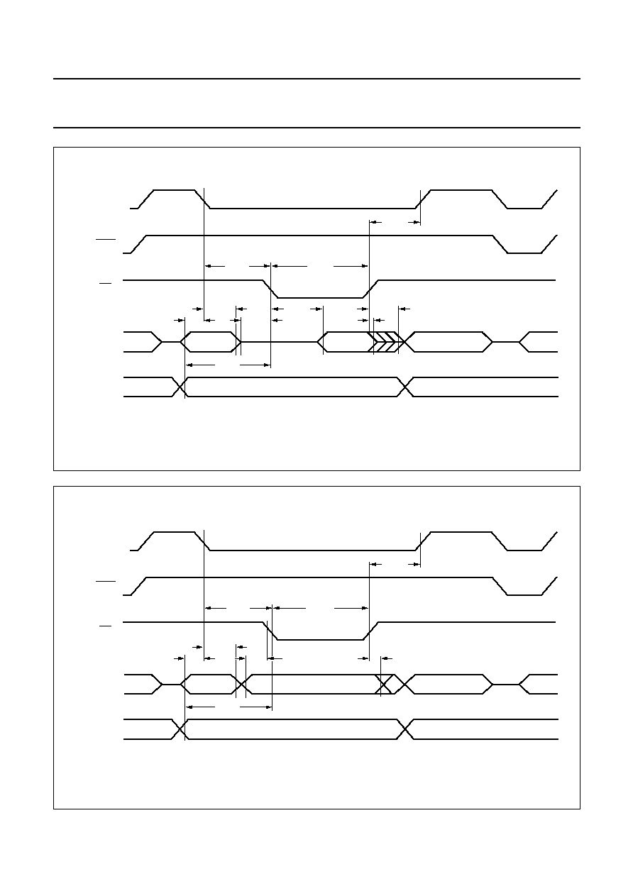
12.3.1
E
XTERNAL DATA MEMORY ACCESS
Table 4
External data memory access (see Fig.6 and
Fig.7)
Note
1. The timings are only valid for the nominal 12 MHz
clock provided to the microcontroller.
12.3.2
S
YMBOL EXPLANATIONS
Each timing symbol has five characters. The first character
is always `t' (time). Depending on their positions, the other
characters indicate the name of a signal or the logical
status of that signal.
The designations are:
A = Address
C = Clock
D = Input data
H = Logic level HIGH
I = Instruction (program memory contents)
L = Logic level LOW, or ALE
P = PSEN
Q = Output data
R = RD signal
t = Time
V = Valid
W = WR signal
X = No longer a valid logic level
Z = Float
Examples:
t
AVLL
= time for address valid to ALE LOW.
t
LLPL
= time for ALE to PSEN LOW.
SYMBOL
PARAMETER
TYPICAL
(1)
UNIT
t
RLRH
RD pulse width
250
ns
t
WLWH
WR pulse width
250
ns
t
RLDV
RD LOW to valid data in 198
ns
t
RHDX
Data hold after RD
0
ns
t
RHDZ
Data float after RD
tbd
ns
t
LLWL
ALE LOW to RD or
WR LOW
132
ns
t
AVWL
Address valid to WR
LOW or RD LOW
172
ns
t
QVWX
Data valid to WR LOW
89
ns
t
WHQX
Data hold after WR
15
ns
t
RLAZ
RD LOW to address
float
tbd
ns
t
WHLH
RD or WR HIGH to
ALE HIGH
40
ns
2005 Mar 09
23
Philips Semiconductors
Product specification
Multi page intelligent teletext decoder
SAA5360; SAA5361
handbook, full pagewidth
GSA082
tLLWL
tRLRH
ALE
PSEN
RD
AD
<
0
:
7
>
A
<
0
:
14
>
, A15_BK,
RAMBK
<
0
:
1
>
A0-A7
DATA IN
A0-A7
INSTR IN
tAVWL
tAVLL
tRHDX
tLLAX
tRLAZ
tRLDV
tRHDZ
tWHLH
Fig.6 External data memory read cycle.
handbook, full pagewidth
GSA083
tLLWL
tWLWH
ALE
PSEN
WR
AD
<
0
:
7
>
A
<
0
:
14
>
, A15_BK,
RAMBK
<
0
:
1
>
A0-A7
DATA OUT
A0-A7 FROM PCL
INSTR IN
tAVWL
tAVLL
tLLAX
tQVWX
tWHQX
tWHLH
Fig.7 External data memory write cycle.

2005 Mar 09
24
Philips Semiconductors
Product specification
Multi page intelligent teletext decoder
SAA5360; SAA5361
13 PACKAGE OUTLINE
UNIT
A
max.
A
1
A
2
A
3
b
p
c
E
(1)
e
H
E
L
L
p
Z
y
w
v
REFERENCES
OUTLINE
VERSION
EUROPEAN
PROJECTION
ISSUE DATE
IEC
JEDEC
JEITA
mm
1.6
0.15
0.05
1.45
1.35
0.25
0.27
0.17
0.20
0.09
14.1
13.9
0.5
16.25
15.75
1.15
0.85
7
0
o
o
0.08
0.08
0.2
1
DIMENSIONS (mm are the original dimensions)
Note
1. Plastic or metal protrusions of 0.25 mm maximum per side are not included.
0.75
0.45
SOT407-1
136E20
MS-026
00-02-01
03-02-20
D
(1)
(1)
(1)
14.1
13.9
H
D
16.25
15.75
E
Z
1.15
0.85
D
b
p
e
E
A
1
A
L
p
detail X
L
(A )
3
B
25
c
D
H
b
p
E
H
A
2
v
M
B
D
ZD
A
Z E
e
v
M
A
X
1
100
76
75
51
50
26
y
pin 1 index
w
M
w
M
0
5
10 mm
scale
LQFP100: plastic low profile quad flat package; 100 leads; body 14 x 14 x 1.4 mm
SOT407-1

2005 Mar 09
25
Philips Semiconductors
Product specification
Multi page intelligent teletext decoder
SAA5360; SAA5361
14 SOLDERING
14.1
Introduction to soldering surface mount
packages
This text gives a very brief insight to a complex technology.
A more in-depth account of soldering ICs can be found in
our
"Data Handbook IC26; Integrated Circuit Packages"
(document order number 9398 652 90011).
There is no soldering method that is ideal for all surface
mount IC packages. Wave soldering can still be used for
certain surface mount ICs, but it is not suitable for fine pitch
SMDs. In these situations reflow soldering is
recommended.
14.2
Reflow soldering
Reflow soldering requires solder paste (a suspension of
fine solder particles, flux and binding agent) to be applied
to the printed-circuit board by screen printing, stencilling or
pressure-syringe dispensing before package placement.
Driven by legislation and environmental forces the
worldwide use of lead-free solder pastes is increasing.
Several methods exist for reflowing; for example,
convection or convection/infrared heating in a conveyor
type oven. Throughput times (preheating, soldering and
cooling) vary between 100 seconds and 200 seconds
depending on heating method.
Typical reflow peak temperatures range from
215
∞
C to 270
∞
C depending on solder paste material. The
top-surface temperature of the packages should
preferably be kept:
∑
below 225
∞
C (SnPb process) or below 245
∞
C (Pb-free
process)
≠ for all BGA, HTSSON..T and SSOP..T packages
≠ for packages with a thickness
2.5 mm
≠ for packages with a thickness < 2.5 mm and a
volume
350 mm
3
so called thick/large packages.
∑
below 240
∞
C (SnPb process) or below 260
∞
C (Pb-free
process) for packages with a thickness < 2.5 mm and a
volume < 350 mm
3
so called small/thin packages.
Moisture sensitivity precautions, as indicated on packing,
must be respected at all times.
14.3
Wave soldering
Conventional single wave soldering is not recommended
for surface mount devices (SMDs) or printed-circuit boards
with a high component density, as solder bridging and
non-wetting can present major problems.
To overcome these problems the double-wave soldering
method was specifically developed.
If wave soldering is used the following conditions must be
observed for optimal results:
∑
Use a double-wave soldering method comprising a
turbulent wave with high upward pressure followed by a
smooth laminar wave.
∑
For packages with leads on two sides and a pitch (e):
≠ larger than or equal to 1.27 mm, the footprint
longitudinal axis is preferred to be parallel to the
transport direction of the printed-circuit board;
≠ smaller than 1.27 mm, the footprint longitudinal axis
must be parallel to the transport direction of the
printed-circuit board.
The footprint must incorporate solder thieves at the
downstream end.
∑
For packages with leads on four sides, the footprint must
be placed at a 45
∞
angle to the transport direction of the
printed-circuit board. The footprint must incorporate
solder thieves downstream and at the side corners.
During placement and before soldering, the package must
be fixed with a droplet of adhesive. The adhesive can be
applied by screen printing, pin transfer or syringe
dispensing. The package can be soldered after the
adhesive is cured.
Typical dwell time of the leads in the wave ranges from
3 seconds to 4 seconds at 250
∞
C or 265
∞
C, depending
on solder material applied, SnPb or Pb-free respectively.
A mildly-activated flux will eliminate the need for removal
of corrosive residues in most applications.
14.4
Manual soldering
Fix the component by first soldering two
diagonally-opposite end leads. Use a low voltage (24 V or
less) soldering iron applied to the flat part of the lead.
Contact time must be limited to 10 seconds at up to
300
∞
C.
When using a dedicated tool, all other leads can be
soldered in one operation within 2 seconds to 5 seconds
between 270
∞
C and 320
∞
C.

2005 Mar 09
26
Philips Semiconductors
Product specification
Multi page intelligent teletext decoder
SAA5360; SAA5361
14.5
Suitability of surface mount IC packages for wave and reflow soldering methods
Notes
1. For more detailed information on the BGA packages refer to the
"(LF)BGA Application Note" (AN01026); order a copy
from your Philips Semiconductors sales office.
2. All surface mount (SMD) packages are moisture sensitive. Depending upon the moisture content, the maximum
temperature (with respect to time) and body size of the package, there is a risk that internal or external package
cracks may occur due to vaporization of the moisture in them (the so called popcorn effect). For details, refer to the
Drypack information in the
"Data Handbook IC26; Integrated Circuit Packages; Section: Packing Methods".
3. These transparent plastic packages are extremely sensitive to reflow soldering conditions and must on no account
be processed through more than one soldering cycle or subjected to infrared reflow soldering with peak temperature
exceeding 217
∞
C
±
10
∞
C measured in the atmosphere of the reflow oven. The package body peak temperature
must be kept as low as possible.
4. These packages are not suitable for wave soldering. On versions with the heatsink on the bottom side, the solder
cannot penetrate between the printed-circuit board and the heatsink. On versions with the heatsink on the top side,
the solder might be deposited on the heatsink surface.
5. If wave soldering is considered, then the package must be placed at a 45
∞
angle to the solder wave direction.
The package footprint must incorporate solder thieves downstream and at the side corners.
6. Wave soldering is suitable for LQFP, QFP and TQFP packages with a pitch (e) larger than 0.8 mm; it is definitely not
suitable for packages with a pitch (e) equal to or smaller than 0.65 mm.
7. Wave soldering is suitable for SSOP, TSSOP, VSO and VSSOP packages with a pitch (e) equal to or larger than
0.65 mm; it is definitely not suitable for packages with a pitch (e) equal to or smaller than 0.5 mm.
8. Image sensor packages in principle should not be soldered. They are mounted in sockets or delivered pre-mounted
on flex foil. However, the image sensor package can be mounted by the client on a flex foil by using a hot bar
soldering process. The appropriate soldering profile can be provided on request.
9. Hot bar soldering or manual soldering is suitable for PMFP packages.
PACKAGE
(1)
SOLDERING METHOD
WAVE
REFLOW
(2)
BGA, HTSSON..T
(3)
, LBGA, LFBGA, SQFP, SSOP..T
(3)
, TFBGA,
VFBGA, XSON
not suitable
suitable
DHVQFN, HBCC, HBGA, HLQFP, HSO, HSOP, HSQFP, HSSON,
HTQFP, HTSSOP, HVQFN, HVSON, SMS
not suitable
(4)
suitable
PLCC
(5)
, SO, SOJ
suitable
suitable
LQFP, QFP, TQFP
not recommended
(5)(6)
suitable
SSOP, TSSOP, VSO, VSSOP
not recommended
(7)
suitable
CWQCCN..L
(8)
, PMFP
(9)
, WQCCN..L
(8)
not suitable
not suitable

2005 Mar 09
27
Philips Semiconductors
Product specification
Multi page intelligent teletext decoder
SAA5360; SAA5361
15 DATA SHEET STATUS
Notes
1. Please consult the most recently issued data sheet before initiating or completing a design.
2. The product status of the device(s) described in this data sheet may have changed since this data sheet was
published. The latest information is available on the Internet at URL http://www.semiconductors.philips.com.
3. For data sheets describing multiple type numbers, the highest-level product status determines the data sheet status.
LEVEL
DATA SHEET
STATUS
(1)
PRODUCT
STATUS
(2)(3)
DEFINITION
I
Objective data
Development
This data sheet contains data from the objective specification for product
development. Philips Semiconductors reserves the right to change the
specification in any manner without notice.
II
Preliminary data Qualification
This data sheet contains data from the preliminary specification.
Supplementary data will be published at a later date. Philips
Semiconductors reserves the right to change the specification without
notice, in order to improve the design and supply the best possible
product.
III
Product data
Production
This data sheet contains data from the product specification. Philips
Semiconductors reserves the right to make changes at any time in order
to improve the design, manufacturing and supply. Relevant changes will
be communicated via a Customer Product/Process Change Notification
(CPCN).
16 DEFINITIONS
Short-form specification
The data in a short-form
specification is extracted from a full data sheet with the
same type number and title. For detailed information see
the relevant data sheet or data handbook.
Limiting values definition
Limiting values given are in
accordance with the Absolute Maximum Rating System
(IEC 60134). Stress above one or more of the limiting
values may cause permanent damage to the device.
These are stress ratings only and operation of the device
at these or at any other conditions above those given in the
Characteristics sections of the specification is not implied.
Exposure to limiting values for extended periods may
affect device reliability.
Application information
Applications that are
described herein for any of these products are for
illustrative purposes only. Philips Semiconductors make
no representation or warranty that such applications will be
suitable for the specified use without further testing or
modification.
17 DISCLAIMERS
Life support applications
These products are not
designed for use in life support appliances, devices, or
systems where malfunction of these products can
reasonably be expected to result in personal injury. Philips
Semiconductors customers using or selling these products
for use in such applications do so at their own risk and
agree to fully indemnify Philips Semiconductors for any
damages resulting from such application.
Right to make changes
Philips Semiconductors
reserves the right to make changes in the products -
including circuits, standard cells, and/or software -
described or contained herein in order to improve design
and/or performance. When the product is in full production
(status `Production'), relevant changes will be
communicated via a Customer Product/Process Change
Notification (CPCN). Philips Semiconductors assumes no
responsibility or liability for the use of any of these
products, conveys no licence or title under any patent,
copyright, or mask work right to these products, and
makes no representations or warranties that these
products are free from patent, copyright, or mask work
right infringement, unless otherwise specified.

© Koninklijke Philips Electronics N.V. 2005
SCA76
All rights are reserved. Reproduction in whole or in part is prohibited without the prior written consent of the copyright owner.
The information presented in this document does not form part of any quotation or contract, is believed to be accurate and reliable and may be changed
without notice. No liability will be accepted by the publisher for any consequence of its use. Publication thereof does not convey nor imply any license
under patent- or other industrial or intellectual property rights.
Philips Semiconductors ≠ a worldwide company
Contact information
For additional information please visit http://www.semiconductors.philips.com.
Fax: +31 40 27 24825
For sales offices addresses send e-mail to: sales.addresses@www.semiconductors.philips.com.
Printed in The Netherlands
R24/06/pp
28
Date of release:
2005 Mar 09
Document order number:
9397 750 14857