 | –≠–ª–µ–∫—Ç—Ä–æ–Ω–Ω—ã–π –∫–æ–º–ø–æ–Ω–µ–Ω—Ç: SAA5561 | –°–∫–∞—á–∞—Ç—å:  PDF PDF  ZIP ZIP |

DATA SHEET
Preliminary specification
Supersedes data of 1999 Aug 02
File under Integrated Circuits, IC02
2000 Feb 23
INTEGRATED CIRCUITS
SAA55xx
Enhanced TV microcontrollers with
On-Screen Display (OSD)

2000 Feb 23
2
Philips Semiconductors
Preliminary specification
Enhanced TV microcontrollers with
On-Screen Display (OSD)
SAA55xx
CONTENTS
1
FEATURES
2
GENERAL DESCRIPTION
3
QUICK REFERENCE DATA
4
ORDERING INFORMATION
5
BLOCK DIAGRAM
6
PINNING INFORMATION
6.1
Pinning
6.2
Pin description
7
MICROCONTROLLER
7.1
Microcontroller features
8
MEMORY ORGANIZATION
8.1
ROM bank switching
8.2
Security bits - program and verify
8.3
RAM organisation
8.4
Data memory
8.5
SFR memory
8.6
Character set feature bits
8.7
External (Auxiliary) memory
9
POWER-ON RESET
10
REDUCED POWER MODES
10.1
Idle mode
10.2
Power-down mode
10.3
Standby mode
11
I/O FACILITY
11.1
I/O ports
11.2
Port type
11.3
Port alternative functions
11.4
LED support
12
INTERRUPT SYSTEM
12.1
Interrupt enable structure
12.2
Interrupt enable priority
12.3
Interrupt vector address
12.4
Level/edge interrupt
13
TIMER/COUNTER
14
WATCHDOG TIMER
14.1
Watchdog Timer operation
15
PULSE WIDTH MODULATORS
15.1
PWM control
15.2
Tuning Pulse Width Modulator (TPWM)
15.3
Software ADC (SAD)
16
I
2
C-BUS SERIAL I/O
16.1
I
2
C-bus port selection
17
MEMORY INTERFACE
17.1
Memory structure
17.2
Memory mapping
17.3
Addressing memory
17.4
Page clearing
18
DATA CAPTURE
18.1
Data Capture features
19
DISPLAY
19.1
Display features
19.2
Display modes
19.3
Display feature descriptions
19.4
Character and attribute coding
19.5
Screen and global controls
19.6
Screen colour
19.7
Text display controls
19.8
Soft scroll action
19.9
Display positioning
19.10
Character set
19.11
ROM addressing
19.12
Redefinable characters
19.13
Display synchronization
19.14
Video/data switch (Fast Blanking) polarity
19.15
Video/Data switch adjustment
19.16
RGB brightness control
19.17
Contrast reduction
20
MEMORY MAPPED REGISTERS (MMR)
21
LIMITING VALUES
22
CHARACTERISTICS
23
QUALITY AND RELIABILITY
23.1
Group A
23.2
Group B
23.3
Group C
24
APPLICATION INFORMATION
25
EMC GUIDELINES
26
REFERENCES
27
PACKAGE OUTLINE
28
SOLDERING
28.1
Introduction to soldering through-hole mount
packages
28.2
Soldering by dipping or by solder wave
28.3
Manual soldering
28.4
Suitability of through-hole mount IC packages
for dipping and wave soldering methods
29
DEFINITIONS
30
LIFE SUPPORT APPLICATIONS
31
PURCHASE OF PHILIPS I
2
C COMPONENTS

2000 Feb 23
3
Philips Semiconductors
Preliminary specification
Enhanced TV microcontrollers with
On-Screen Display (OSD)
SAA55xx
1
FEATURES
∑
Single-chip microcontroller with integrated OSD
∑
Versions available with integrated data capture
∑
OTP memory for both program ROM and character sets
∑
Single power supply: 3.0 to 3.6 V
∑
5 V tolerant digital inputs and I/O
∑
29 I/O ports via individual addressable controls
∑
Programmable I/O for push-pull, open-drain and
quasi-bidirectional
∑
Two port lines with 8 mA sink (at <0.4 V) capability, for
direct drive of LED
∑
Single crystal oscillator for microcontroller, OSD and
data capture
∑
Power reduction modes: Idle, Power-down and Standby
∑
Byte level I
2
C-bus interface with dual port I/O
∑
32 Dynamically Redefinable Characters for OSDs
∑
Special graphic characters allowing four colours per
character
∑
Selectable character height 9, 10, 13 and 16 TV lines
∑
Pin compatibility throughout family
∑
Operating temperature:
-
20 to +70
∞
C.
2
GENERAL DESCRIPTION
The SAA55xx family of microcontrollers are a derivative of
the Philips industry-standard 80C51 microcontroller and
are intended for use as the central control mechanism in a
television receiver. They provide control functions for the
television system, On-Screen Display (OSD) and some
versions include an integrated data capture and display
function.
The data capture hardware has the capability of decoding
and displaying both 525 and 625-line World System
Teletext (WST), Closed Caption (CC) information, Video
Programming Information (VPS) and Wide Screen
Signalling (WSS) information. The same display hardware
is used both for Teletext, Closed Caption and On-Screen
Display, which means that the display features available
give greater flexibility to differentiate the TV set.
The SAA55xx family offers a range of functionality from
non-text, 16-kbyte program ROM and 256-byte RAM, to a
10 page text version, 128-kbyte program ROM and
2.25-kbyte RAM.
3
QUICK REFERENCE DATA
SYMBOL
PARAMETER
MIN.
TYP.
MAX.
UNIT
Supply
V
DDX
any supply voltage (V
DD
to V
SS
)
3.0
3.3
3.6
V
I
DDP
periphery supply current
1
-
-
mA
I
DDC
core supply current
-
15
18
mA
I
DDC(id)
Idle mode core supply current
-
4.6
6
mA
I
DDC(pd)
Power-down mode core supply current
-
0.76
1
mA
I
DDC(stb)
standby mode core supply current
-
5.1
9
mA
I
DDA
analog supply current
-
45
48
mA
I
DDA(id)
Idle mode analog supply current
-
0.87
1.0
mA
I
DDA(stb)
standby mode analog supply current
-
809
950
µ
A
I
DDA(pd)
Power-down mode analog supply current
-
0.45
0.7
mA
f
xtal
crystal frequency
-
12
-
MHz
T
amb
ambient temperature
-
20
-
+70
∞
C
T
stg
storage temperature
-
55
-
+125
∞
C
2000 Feb 23
4
Philips Semiconductors
Preliminary specification
Enhanced TV microcontrollers with
On-Screen Display (OSD)
SAA55xx
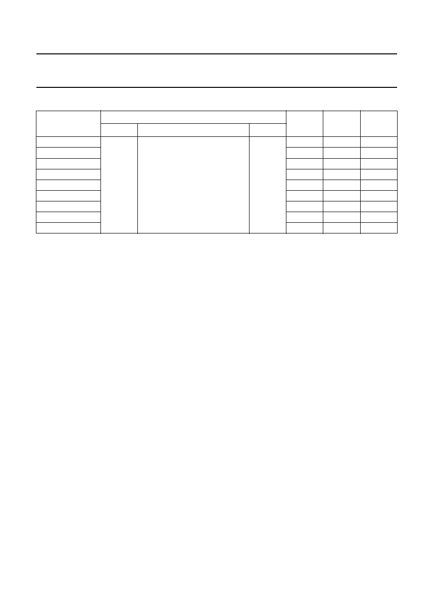
4
ORDERING INFORMATION
Notes
1. `nnnn' is a four digit number uniquely referencing the microcontroller program mask.
2. For details of the LQFP100 package, please contact your local regional sales office for availability.
TYPE NUMBER
(1)
PACKAGE
(2)
ROM
RAM
TEXT
PAGES
NAME
DESCRIPTION
VERSION
SAA5530PS/nnnn
SDIP52
plastic shrink dual in-line package;
52 leads (600 mil)
SOT247-1
16-kbyte
256-byte
1
SAA5531PS/nnnn
32-kbyte
512-byte
1
SAA5532PS/nnnn
48-kbyte
750-byte
1
SAA5533PS/nnnn
64-kbyte
1-kbyte
1
SAA5561PS/nnnn
32-kbyte
750-byte
10
SAA5562PS/nnnn
48-kbyte
1-kbyte
10
SAA5563PS/nnnn
64-kbyte
1.2-kbyte
10
SAA5564PS/nnnn
96-kbyte
1.5-kbyte
10
SAA5565PS/nnnn
128-kbyte
2-kbyte
10

2000 Feb 23
5
Philips Semiconductors
Preliminary specification
Enhanced TV microcontrollers with
On-Screen Display (OSD)
SAA55xx
5
BLOCK DIAGRAM
Fig.1 Block diagram (top level architecture).
handbook, full pagewidth
MBK950
MICROPROCESSOR
(80C51)
SRAM
(256-BYTE)
ROM
(16 TO 128-KBYTE)
MEMORY
INTERFACE
DISPLAY
R
G
B
VDS
VSYNC
HSYNC
CVBS
DATA
CAPTURE
DRAM
(3 TO 12-KBYTE)
TV CONTROL
AND
INTERFACE
I
2
C-bus, general I/O
DISPLAY
TIMING
CVBS
DATA
CAPTURE
TIMING
2000 Feb 23
6
Philips Semiconductors
Preliminary specification
Enhanced TV microcontrollers with
On-Screen Display (OSD)
SAA55xx
6
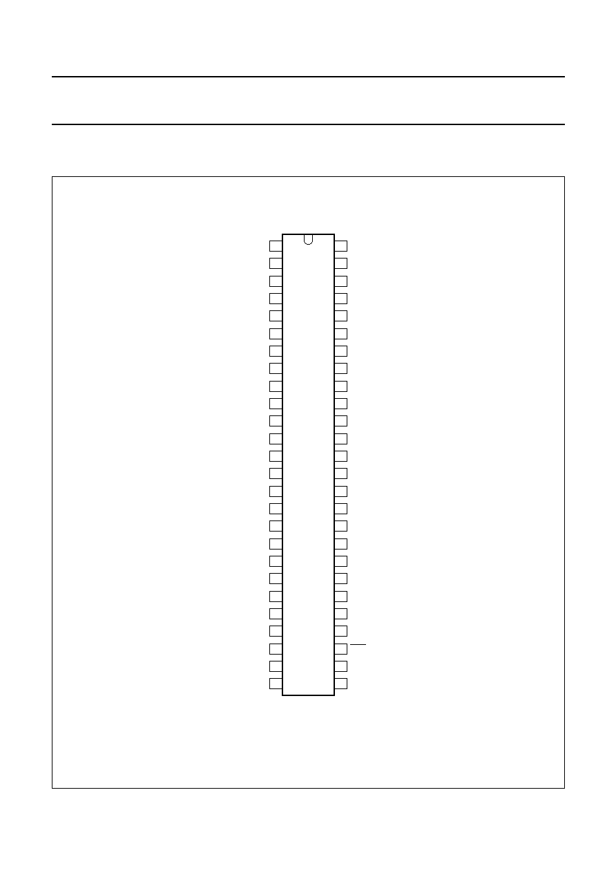
PINNING INFORMATION
6.1
Pinning
Fig.2 SDIP52 pin configuration.
handbook, halfpage
SAA55xx
MBK951
1
2
3
4
5
6
7
8
9
10
11
12
13
14
15
16
17
18
19
20
21
22
23
24
25
26
P2.0/TPWM
P2.1/PWM0
P2.2/PWM1
P2.3/PWM2
P2.4/PWM3
P2.5/PWM4
P2.6/PWM5
P2.7/PWM6
P3.0/ADC0
P3.1/ADC1
P3.2/ADC2
P3.3/ADC3
VSSC
P0.0
P0.1
P0.2
P0.3
P0.4
P0.5
P0.6
P0.7
VSSA
CVBS0
CVBS1
SYNC_FILTER
IREF
P1.5/SDA1
P1.4/SCL1
P1.7/SDA0
P1.6/SCL0
P1.3/T1
P1.2/INT0
P1.1/T0
P1.0/INT1
VDDP
RESET
XTALOUT
XTALIN
OSCGND
VDDC
VSSP
VSYNC
HSYNC
VDS
R
G
B
VDDA
P3.4/PWM7
COR
VPE
FRAME
52
51
50
49
48
47
46
45
44
43
42
41
40
39
38
37
36
35
34
33
32
31
30
29
28
27
2000 Feb 23
7
Philips Semiconductors
Preliminary specification
Enhanced TV microcontrollers with
On-Screen Display (OSD)
SAA55xx
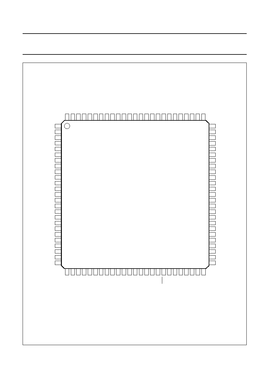
Fig.3 LQFP100 pin configuration.
handbook, full pagewidth
75
74
73
72
71
70
69
68
67
66
65
64
63
62
61
60
59
58
57
56
55
54
53
52
51
25
24
23
22
21
20
19
18
17
16
15
14
13
12
11
10
9
8
7
6
5
4
3
2
1
P3.7
P0.4
n.c.
P0.3
n.c.
n.c.
n.c.
P0.2
P0.1
P0.0
n.c.
n.c.
P0.5
VSSP
VSSC
n.c.
n.c.
n.c.
n.c.
P3.3/ADC3
P3.2/ADC2
P3.1/ADC1
n.c.
P3.0/ADC0
P2.7/PWM6
n.c.
VDS
HSYNC
P3.5
VSYNC
n.c.
n.c.
n.c.
P3.6
VSSP
n.c.
VPE_2
VDDC
n.c.
n.c.
n.c.
n.c.
n.c.
OSCGND
XTALIN
XTALOUT
n.c.
RESET
n.c.
VDDP
100
99
98
97
96
95
94
93
92
91
90
89
88
87
86
85
84
83
82
81
80
79
78
77
76
P2.0/TPWM
n.c.
P2.6/PWM5
P2.5/PWM4
P2.4/PWM3
P2.3/PWM2
P2.2/PWM1
P2.1/PWM0
n.c.
n.c.
n.c.
n.c.
n.c.
n.c.
n.c.
n.c.
P1.5/SDA1
P1.4/SCL1
P1.7/SDA0
P1.6/SCL0
P1.3/T1
P1.2/INT0
P1.1/T0
n.c.
P1.0/INT1
n.c.
n.c.
P0.6
P0.7
V
SSA
CVBS0
CVBS1
n.c.
SYNC_FILTER
IREF
n.c.
n.c.
n.c.
n.c.
n.c.
FRAME
VPE
COR
P3.4/PWM7
V
DDA
B
G
R
n.c.
n.c.
26
27
28
29
30
31
32
33
34
35
36
37
38
39
40
41
42
43
44
45
46
47
48
49
50
GSA001
SAA55xx
2000 Feb 23
8
Philips Semiconductors
Preliminary specification
Enhanced TV microcontrollers with
On-Screen Display (OSD)
SAA55xx
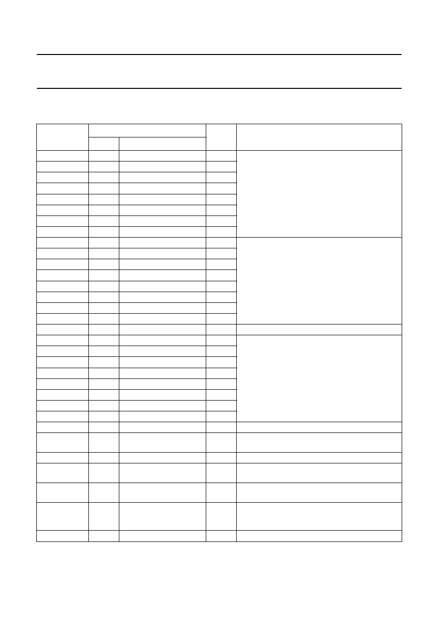
6.2
Pin description
Table 1
SDIP52 and LQFP100 packages
SYMBOL
PIN
TYPE
DESCRIPTION
SDIP52
LQFP100
P2.0/TPWM
1
100
I/O
Port 2. 8-bit programmable bidirectional port with
alternative functions.
P2.0/TPWM is the output for the 14-bit high
precision PWM; P2.1/PWM0 to P2.7/PWM6 are the
outputs for the 6-bit PWMs 0 to 6.
P2.1/PWM0
2
93
I/O
P2.2/PWM1
3
94
I/O
P2.3/PWM2
4
95
I/O
P2.4/PWM3
5
96
I/O
P2.5/PWM4
6
97
I/O
P2.6/PWM5
7
98
I/O
P2.7/PWM6
8
1
I/O
P3.0/ADC0
9
2
I/O
Port 3. 8-bit programmable bidirectional port with
alternative functions.
P3.0/ADC0 to P3.3/ADC3 are the inputs for the
software ADC facility and P3.4/PWM7 is the output
for the 6-bit PWM7. P3.5 to P3.7 have no alternative
functions and are only available with the LQFP100
package.
P3.1/ADC1
10
4
I/O
P3.2/ADC2
11
5
I/O
P3.3/ADC3
12
6
I/O
P3.4/PWM7
30
44
I/O
P3.5
-
54
I/O
P3.6
-
59
I/O
P3.7
-
25
I/O
V
SSC
13
11
-
core ground
P0.0
14
16
I/O
Port 0. 8-bit programmable bidirectional port.
P0.5 and P0.6 have 8 mA current sinking capability
for direct drive of LEDs.
P0.1
15
17
I/O
P0.2
16
18
I/O
P0.3
17
22
I/O
P0.4
18
24
I/O
P0.5
19
13
I/O
P0.6
20
28
I/O
P0.7
21
29
I/O
V
SSA
22
30
-
analog ground
CVBS0
23
31
I
Composite video input. A positive-going 1 V
(peak-to-peak) input is required.
CVBS1
24
32
I
connected via a 100 nF capacitor
SYNC_FILTER
25
34
I
CVBS sync filter input. This pin should be
connected to V
SSA
via a 100 nF capacitor.
IREF
26
35
I
Reference current input for analog circuits,
connected to V
SSA
via a 24 k
resistor.
FRAME
27
41
O
De-interlace output synchronized with the VSYNC
pulse to produce a non-interlaced display by
adjustment of the vertical deflection circuits.
VPE
28
42
I
OTP programming voltage

2000 Feb 23
9
Philips Semiconductors
Preliminary specification
Enhanced TV microcontrollers with
On-Screen Display (OSD)
SAA55xx
COR
29
43
O
Open-drain, active LOW output which allows
selective contrast reduction of the TV picture to
enhance a mixed mode display.
V
DDA
31
45
-
+3.3 V analog power supply
B
32
46
O
pixel rate output of the BLUE colour information
G
33
47
O
pixel rate output of the GREEN colour information
R
34
48
O
pixel rate output of the RED colour information
VDS
35
52
O
video/data switch push-pull output for dot rate fast
blanking
HSYNC
36
53
I
Schmitt triggered input for a TTL-level version of the
horizontal sync pulse; the polarity of this pulse is
programmable by register bit TXT1.H POLARITY.
VSYNC
37
55
I
Schmitt triggered input for a TTL-level version of the
vertical sync pulse; the polarity of this pulse is
programmable by register bit TXT1.V POLARITY.
V
SSP
38
12, 60
-
periphery ground
V
DDC
39
63
-
+3.3 V core power supply
OSCGND
40
69
-
crystal oscillator ground
XTALIN
41
70
I
12 MHz crystal oscillator input
XTALOUT
42
71
O
12 MHz crystal oscillator output
RESET
43
73
I
If the reset input is HIGH for at least 2 machine
cycles (24 oscillator periods) while the oscillator is
running, the device is reset; this pin should be
connected to V
DDP
via a capacitor.
V
DDP
44
75
-
+3.3 V periphery power supply
P1.0/INT1
45
76
I/O
Port 1. 8-bit programmable bidirectional port with
alternative functions.
P1.0/INT1 is external interrupt 1 which can be
triggered on the rising and falling edge of the pulse.
P1.1/T0 is the Counter/Timer 0. P1.2/INT0 is
external interrupt 0. P1.3/T1 is the Counter/Timer 1.
P1.6/SCL0 is the serial clock input for the I
2
C-bus
and P1.7/SDA0 is the serial data port for the
I
2
C-bus. P1.4/SCL1 is the serial clock input for the
I
2
C-bus and P1.5/SDA1 is the serial data port for the
I
2
C-bus.
P1.1/T0
46
78
I/O
P1.2/INT0
47
79
I/O
P1.3/T1
48
80
I/O
P1.6/SCL0
49
81
I/O
P1.7/SDA0
50
82
I/O
P1.4/SCL1
51
83
I/O
P1.5/SDA1
52
58
I/O
VPE-2
-
62
I
OTP programming voltage
n.c.
-
3, 7 to 10,14, 15, 19 to 21,
23, 26, 27, 33, 36 to 40,
49 to 51, 56 to 58, 61,
64 to 68, 72, 74, 77,
85 to 92, 99
-
not connected
SYMBOL
PIN
TYPE
DESCRIPTION
SDIP52
LQFP100

2000 Feb 23
10
Philips Semiconductors
Preliminary specification
Enhanced TV microcontrollers with
On-Screen Display (OSD)
SAA55xx
7
MICROCONTROLLER
The functionality of the microcontroller used on this device
is described here with reference to the industry standard
80C51 microcontroller. A full description of its functionality
can be found in
"Handbook IC20, 80C51-Based 8-bit
Microcontrollers".
7.1
Microcontroller features
∑
80C51 microcontroller core standard instruction set and
timing
∑
1
µ
s machine cycle
∑
Maximum 128K
◊
8-bit Program ROM
∑
Maximum of 12K
◊
8-bit Auxiliary RAM
∑
Interrupt Controller for individual enable/disable with two
level priority
∑
Two 16-bit Timer/Counter registers
∑
Watchdog Timer
∑
Auxiliary RAM page pointer
∑
16-bit Data pointer
∑
Idle and Power-down mode
∑
29 general I/O lines
∑
Eight 6-bit Pulse Width Modulator (PWM) outputs for
control of TV analog signals
∑
One 14-bit PWM for Voltage Synthesis Tuner (VST)
control
∑
8-bit ADC with 4 multiplexed inputs
∑
2 high current outputs for directly driving LEDs etc.
∑
I
2
C byte level bus interface with dual ports.
8
MEMORY ORGANIZATION
The device has the capability of a maximum of 128-kbyte
Program ROM and 12-kbyte Data RAM internally.
8.1
ROM bank switching
The 64-kbyte device has a continuous address space from
0 to 64 kbytes. The 128-kbyte memory is arranged in four
banks of 32 kbytes. One of the 32-kbyte banks is common
and is always addressable. The other three banks
(Bank 0, Bank 1 and Bank 2) can be accessed by
selecting the right bank via the SFR ROMBK bits; see
Table 2.
The ROM bank switching is handled and supported by the
compiler and linker development tools.
Table 2
ROM bank selection
8.2
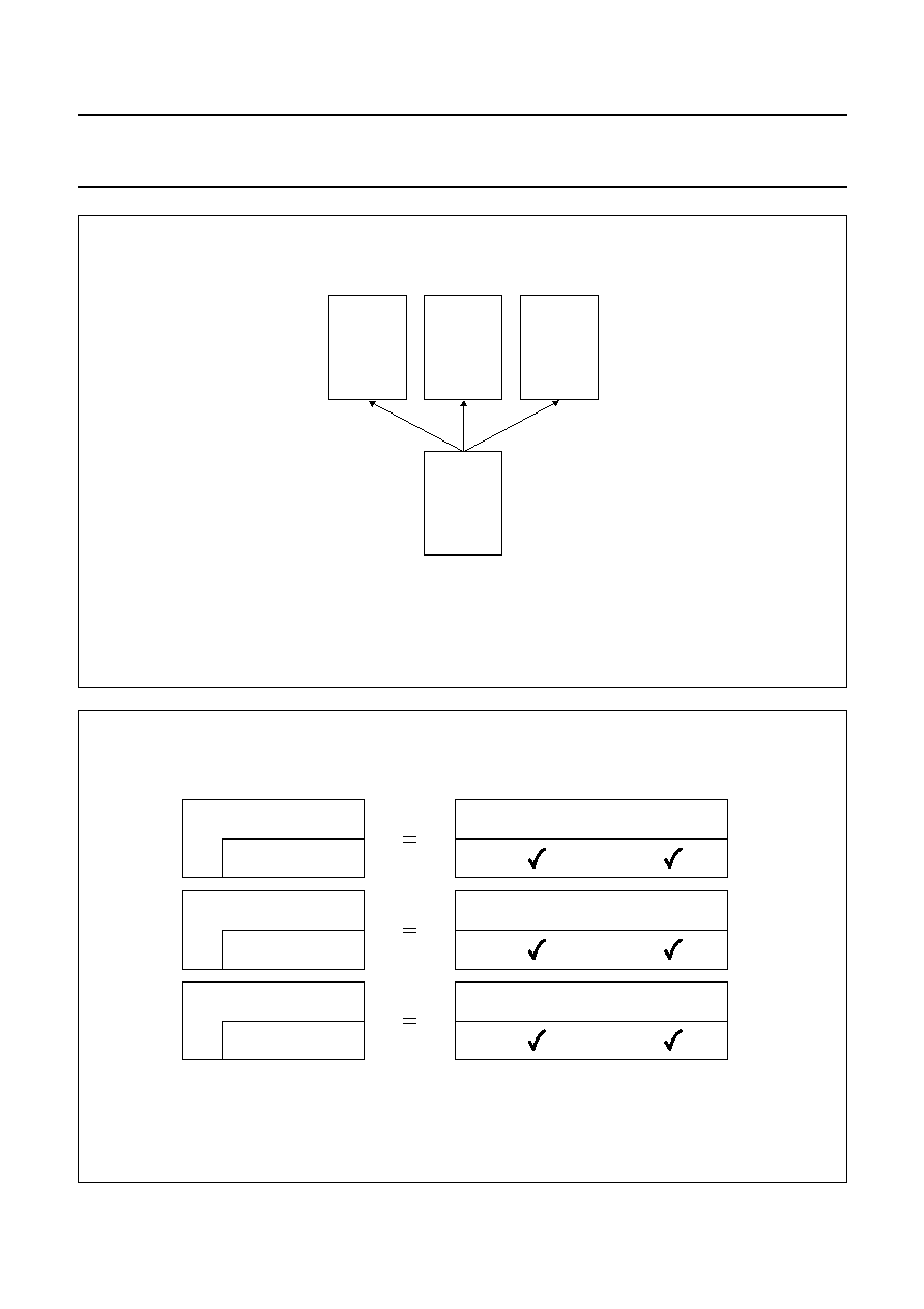
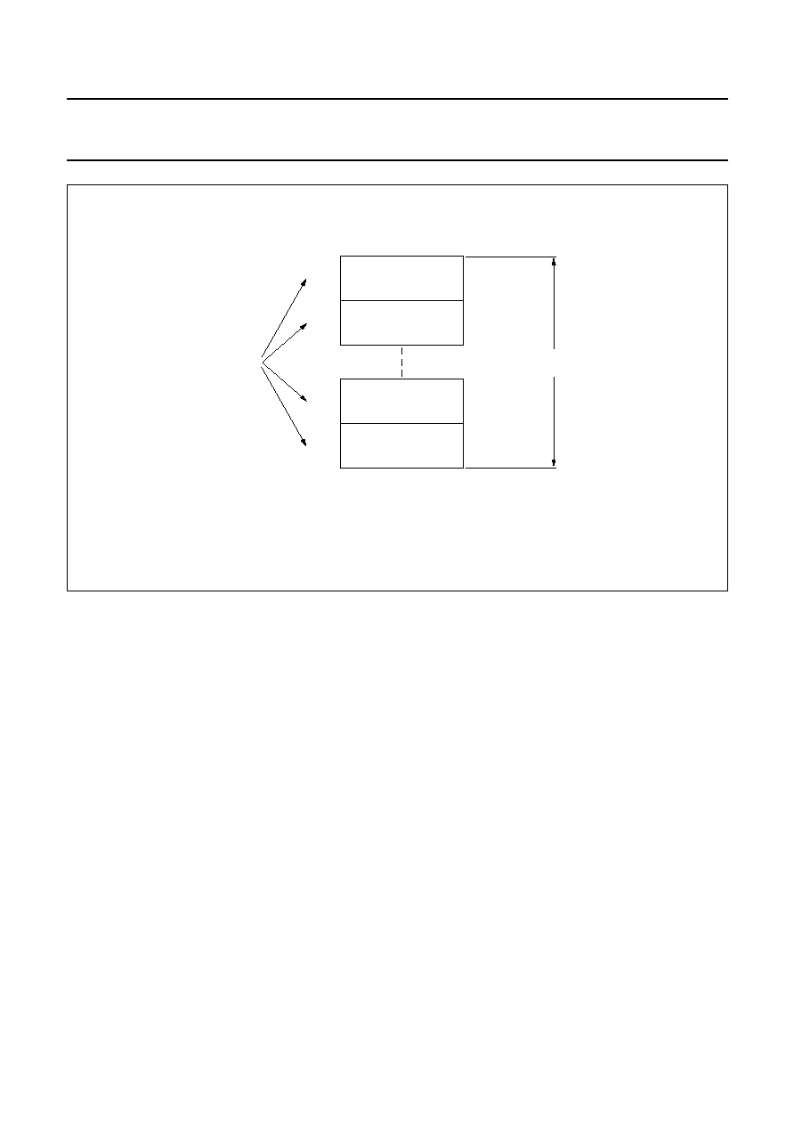
Security bits - program and verify
SAA55xx devices have a set of security bits allied with
each section of the device, i.e. Program ROM, Character
ROM and Packet 26 ROM. The security bits are used to
prevent the ROM from being overwritten once
programmed, and also the contents being verified once
programmed. The security bits are one-time
programmable and cannot be erased.
The SAA55xx memory and security bits are structured as
shown in Fig.5. The SAA55xx security bits are set as
shown in Fig.6 for production programmed devices and
are set as shown in Fig.7 for production blank devices.
8.3
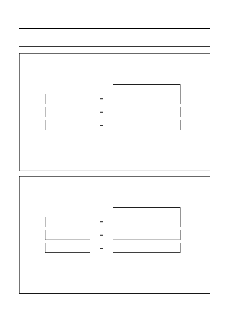
RAM organisation
The internal Data RAM is organised into two areas, Data
memory and Special Function Registers (SFRs) as shown
in Fig.8.
8.4
Data memory
The Data memory is 256
◊
8 bits and occupies the
address range 00H to FFH when using indirect addressing
and 00H to 7FH when using direct addressing. The SFRs
occupy the address range 80H to FFH and are accessible
using direct addressing only.
The lower 128 bytes of Data memory are mapped as
shown in Fig.9. The lowest 24 bytes are grouped into
4 banks of 8 registers, the next 16 bytes above the register
banks form a block of bit addressable memory space.
The upper 128 bytes is not allocated for any special area
or functions.
Table 3
Bank selection
ROMBK1 ROMBK0 0 TO 32-kbyte 32 TO 64-kbyte
0
0
common
Bank 0
0
1
common
Bank 1
1
0
common
Bank 2
1
1
reserved
reserved
RS1
RS0
BANK
0
0
Bank 0
0
1
Bank 1
1
0
Bank 2
1
1
Bank 3
2000 Feb 23
11
Philips Semiconductors
Preliminary specification
Enhanced TV microcontrollers with
On-Screen Display (OSD)
SAA55xx
Fig.4 ROM bank switching memory map.
handbook, halfpage
MBK952
7FFFH
0000H
COMMON
(32-KBYTE)
FFFFH
8000H
BANK 1
(32-KBYTE)
FFFFH
8000H
BANK 2
(32-KBYTE)
FFFFH
8000H
BANK 0
(32-KBYTE)
Fig.5 Memory and security bit structures.
handbook, full pagewidth
MBK953
PROGRAM ROM
MEMORY
USER ROM PROGRAMMING
(ENABLE/DISABLE)
VERIFY
(ENABLE/DISABLE)
SECURITY BITS INTERACTION
USER ROM
(128K x 8-BIT)
CHARACTER ROM
USER ROM
(9K x 12-BIT)
PACKET 26 ROM
USER ROM
(4K x 8-BIT)
USER ROM PROGRAMMING
(ENABLE/DISABLE)
VERIFY
(ENABLE/DISABLE)
USER ROM PROGRAMMING
(ENABLE/DISABLE)
VERIFY
(ENABLE/DISABLE)
2000 Feb 23
12
Philips Semiconductors
Preliminary specification
Enhanced TV microcontrollers with
On-Screen Display (OSD)
SAA55xx
Fig.6 Security bits for production devices.
handbook, full pagewidth
MBK954
PROGRAM ROM
MEMORY
USER ROM PROGRAMMING
(ENABLE/DISABLE)
VERIFY
(ENABLE/DISABLE)
DISABLED
ENABLED
DISABLED
ENABLED
DISABLED
ENABLED
SECURITY BITS SET
CHARACTER ROM
PACKET 26 ROM
Fig.7 Security bits for production blank devices.
handbook, full pagewidth
MBK955
PROGRAM ROM
MEMORY
USER ROM PROGRAMMING
(ENABLE/DISABLE)
VERIFY
(ENABLE/DISABLE)
ENABLED
ENABLED
ENABLED
ENABLED
ENABLED
ENABLED
SECURITY BITS SET
CHARACTER ROM
PACKET 26 ROM

2000 Feb 23
13
Philips Semiconductors
Preliminary specification
Enhanced TV microcontrollers with
On-Screen Display (OSD)
SAA55xx
Fig.8 Internal Data memory.
handbook, halfpage
MBK956
accessible
by indirect
addressing
only
DATA
MEMORY
FFH
upper 128 bytes
lower 128 bytes
80H
7FH
00H
SPECIAL
FUNCTION
REGISTERS
accessible
by direct
and indirect
addressing
accessible
by direct
addressing
only
Fig.9 Lower 128 bytes of internal RAM.
handbook, halfpage
MGM677
R7
R0
07H
0
R7
R0
0FH
08H
R7
R0
17H
10H
R7
R0
1FH
18H
2FH
7FH
20H
30H
bit-addressable space
(bit addresses 00H to 7FH)
4 banks of 8 registers
(R0 to R7)

2000
Feb
23
14
Philips Semiconductors
Preliminar
y specification
Enhanced TV microcontrollers with
On-Screen Displa
y (OSD)
SAA55xx
This text is here in white to force landscape pages to be rotated correctly when browsing through the pdf in the Acrobat reader.This text is here in
_
white to force landscape pages to be rotated correctly when browsing through the pdf in the Acrobat reader.This text is here inThis text is here in
white to force landscape pages to be rotated correctly when browsing through the pdf in the Acrobat reader. white to force landscape pages to be ...
8.5
SFR memory
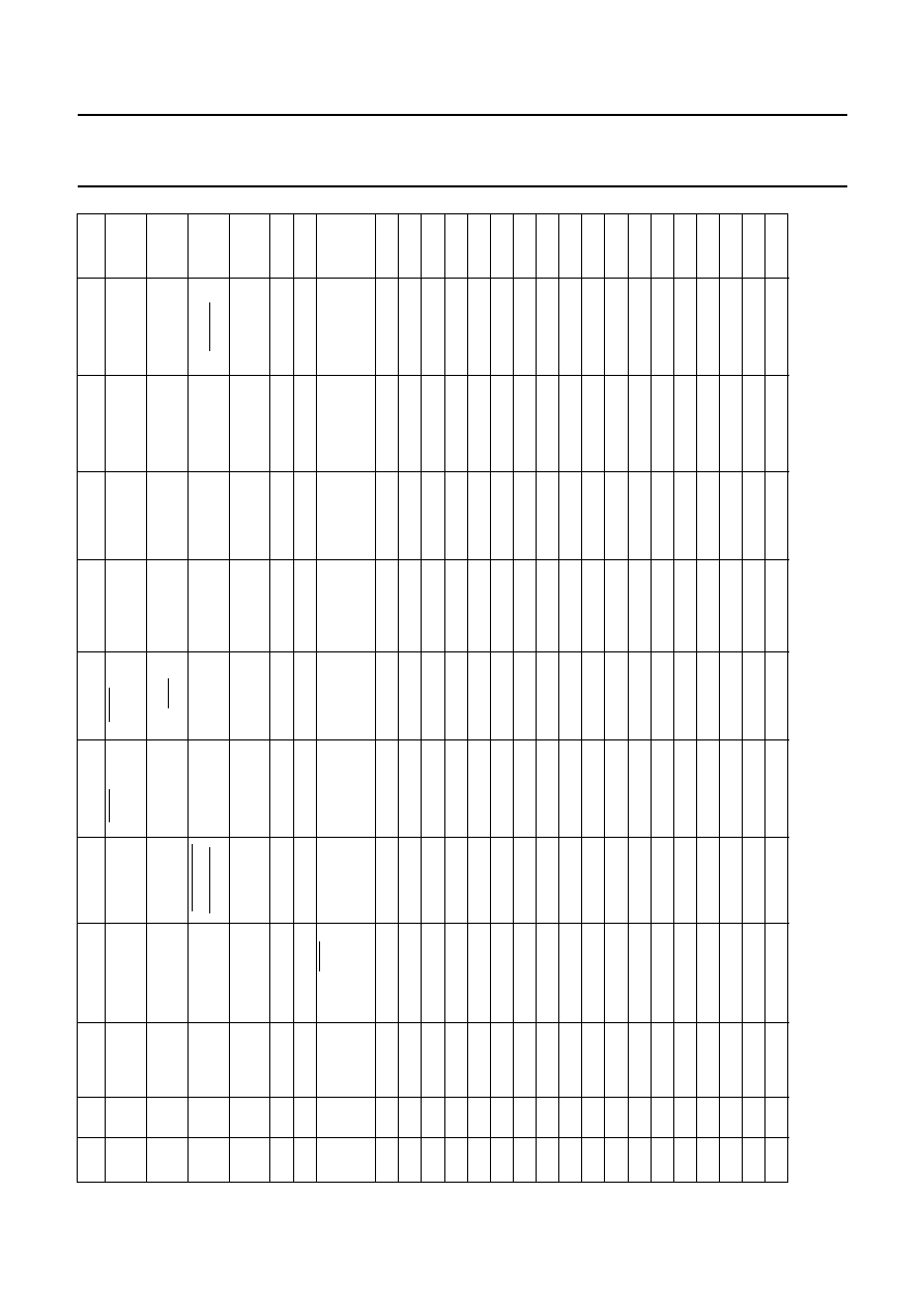
The Special Function Register (SFR) space is used for port latches, timer, peripheral control, acquisition control, display control, etc. These registers
can only be accessed by direct addressing. Sixteen of the addresses in the SFR space are both bit and byte addressable. The bit addressable SFRs
are those whose address ends in 0H or 8H. A summary of the SFR map in address order is shown in Table 4.
A description of each of the SFR bits is shown in Table 5 which presents the SFRs in alphabetical order.
Table 4
SFR memory map
ADD R/W
NAME
7
6
5
4
3
2
1
0
RESET
80H
R/W
P0
P07
P06
P05
P04
P03
P02
P01
P00
FFH
81H
R/W
SP
SP7
SP6
SP5
SP4
SP3
SP2
SP1
SP0
07H
82H
R/W
DPL
DPL7
DPL6
DPL5
DPL4
DPL3
DPL2
DPL1
DPL0
00H
83H
R/W
DPH
DPH7
DPH6
DPH5
DPH4
DPH3
DPH2
DPH1
DPH0
00H
87H
R/W
PCON
0
ARD
RFI
WLE
GF1
GF0
PD
IDL
00H
88H
R/W
TCON
TF1
TR1
TF0
TR0
IE1
IT1
IE0
IT0
00H
89H
R/W
TMOD
GATE
C/T
M1
M0
GATE
C/T
M1
M0
00H
8AH
R/W
TL0
TL07
TL06
TL05
TL04
TL03
TL02
TL01
TL00
00H
8BH
R/W
TL1
TL17
TL16
TL15
TL14
TL13
TL12
TL11
TL10
00H
8CH R/W
TH0
TH07
TH06
TH05
TH04
TH03
TH02
TH01
TH00
00H
8DH R/W
TH1
TH17
TH16
TH15
TH14
TH13
TH12
TH11
TH10
00H
90H
R/W
P1
P17
P16
P15
P14
P13
P12
P11
P10
FFH
96H
R/W
P0CFGA
P0CFGA7
P0CFGA6
P0CFGA5
P0CFGA4
P0CFGA3
P0CFGA2
P0CFGA1
P0CFGA0
FFH
97H
R/W
P0CFGB
P0CFGB7
P0CFGB6
P0CFGB5
P0CFGB4
P0CFGB3
P0CFGB2
P0CFGB1
P0CFGB0
00H
98H
R/W
SADB
0
0
0
DC_COMP
SAD3
SAD2
SAD1
SAD0
00H
9EH
R/W
P1CFGA
P1CFGA7
P1CFGA6
P1CFGA5
P1CFGA4
P1CFGA3
P1CFGA2
P1CFGA1
P1CFGA0
FFH
9FH
R/W
P1CFGB
P1CFGB7
P1CFGB6
P1CFGB5
P1CFGB4
P1CFGB3
P1CFGB2
P1CFGB1
P1CFGB0
00H
A0H
R/W
P2
P27
P26
P25
P24
P23
P22
P21
P20
FFH
A6H
R/W
P2CFGA
P2CFGA7
P2CFGA6
P2CFGA5
P2CFGA4
P2CFGA3
P2CFGA2
P2CFGA1
P2CFGA0
FFH
A7H
R/W
P2CFGB
P2CFGB7
P2CFGB6
P2CFGB5
P2CFGB4
P2CFGB3
P2CFGB2
P2CFGB1
P2CFGB0
00H
A8H
R/W
IE
EA
EBUSY
ES2
ECC
ET1
EX1
ET0
EX0
00H
B0H
R/W
P3
P37
P36
P35
P34
P33
P32
P31
P30
FFH

2000
Feb
23
15
Philips Semiconductors
Preliminar
y specification
Enhanced TV microcontrollers with
On-Screen Displa
y (OSD)
SAA55xx
This text is here in white to force landscape pages to be rotated correctly when browsing through the pdf in the Acrobat reader.This text is here in
_
white to force landscape pages to be rotated correctly when browsing through the pdf in the Acrobat reader.This text is here inThis text is here in
white to force landscape pages to be rotated correctly when browsing through the pdf in the Acrobat reader. white to force landscape pages to be ...
B2H
R/W
TXT18
NOT3
NOT2
NOT1
NOT0
0
0
BS1
BS0
00H
B3H
R/W
TXT19
TEN
TC2
TC1
TC0
0
0
TS1
TS0
00H
B4H
R/W
TXT20
DRCS
ENABLE
OSD
PLANES
0
0
OSD LANG
ENABLE
OSD LAN2
OSD LAN1
OSD LAN0
00H
B5H
R/W
TXT21
DISP
LINES1
DISP
LINES0
CHAR SIZE1
CHAR
SIZE0
I
2
C PORT 1
CC ON
I
2
C PORT 0
CC/TXT
02H
B6H
R
TXT22
GPF7
GPF6
GPF5
GPF4
GPF3
GPF2
GPF1
1
XXH
B7H
R/W
CCLIN
0
0
0
CS4
CS3
CS2
CS1
CS0
15H
B8H
R/W
IP
0
PBUSY
PES2
PCC
PT1
PX1
PT0
PX0
00H
B9H
R/W
TXT17
0
FORCE
ACQ1
FORCE
ACQ0
FORCE
DISP1
FORCE
DISP0
SCREEN
COL2
SCREEN
COL1
SCREEN
COL0
00H
BAH
R
WSS1
0
0
0
WSS<3:0>
ERROR
WSS3
WSS2
WSS1
WSS0
00H
BBH
R
WSS2
0
0
0
WSS<7:4>
ERROR
WSS7
WSS6
WSS5
WSS4
00H
BCH
R
WSS3
WSS<13:11>
ERROR
WSS13
WSS12
WSS11
WSS<10:8>
ERROR
WSS10
WSS9
WSS8
00H
BEH R/W
P3CFGA
1
1
1
P3CFGA4
P3CFGA3
P3CFGA2
P3CFGA1
P3CFGA0
FFH
BFH R/W
P3CFGB
0
0
0
P3CFGB4
P3CFGB3
P3CFGB2
P3CFGB1
P3CFGB0
00H
C0H R/W
TXT0
X24 POSN
DISPLAY
X24
AUTO
FRAME
DISABLE
HEADER
ROLL
DISPLAY
STATUS
ROW ONLY
DISABLE
FRAME
VPS ON
INV ON
00H
C1H R/W
TXT1
EXT PKT
OFF
8-BIT
ACQ OFF
X26 OFF
FULL
FIELD
FIELD
POLARITY
H
POLARITY
V
POLARITY
00H
C2H R/W
TXT2
ACQ BANK
REQ3
REQ2
REQ1
REQ0
SC2
SC1
SC0
00H
C3H
W
TXT3
-
-
-
PRD4
PRD3
PRD2
PRD1
PRD0
00H
C4H R/W
TXT4
OSD BANK
ENABLE
QUAD
WIDTH
ENABLE
EAST/WEST
DISABLE
DOUBLE
HEIGHT
B MESH
ENABLE
C MESH
ENABLE
TRANS
ENABLE
SHADOW
ENABLE
00H
C5H R/W
TXT5
BKGND OUT
BKGND IN
COR OUT
COR IN
TEXT OUT
TEXT IN
PICTURE
ON OUT
PICTURE
ON IN
03H
ADD R/W
NAME
7
6
5
4
3
2
1
0
RESET
2000
Feb
23
16
Philips Semiconductors
Preliminar
y specification
Enhanced TV microcontrollers with
On-Screen Displa
y (OSD)
SAA55xx
This text is here in white to force landscape pages to be rotated correctly when browsing through the pdf in the Acrobat reader.This text is here in
_
white to force landscape pages to be rotated correctly when browsing through the pdf in the Acrobat reader.This text is here inThis text is here in
white to force landscape pages to be rotated correctly when browsing through the pdf in the Acrobat reader. white to force landscape pages to be ...
C6H R/W
TXT6
BKGND OUT
BKGND IN
COR OUT
COR IN
TEXT OUT
TEXT IN
PICTURE
ON OUT
PICTURE
ON IN
03H
C7H R/W
TXT7
STATUS
ROW TOP
CURSOR
ON
REVEAL
BOTTOM
/TOP
DOUBLE
HEIGHT
BOX ON 24
BOX ON
1-23
BOX ON 0
00H
C8H R/W
TXT8
(reserved)
0
FLICKER
STOP ON
(reserved)
0
DISABLE
SPANISH
PKT 26
RECEIVED
WSS
RECEIVED
WSS ON
CVBS1/
CVBS0
00H
C9H R/W
TXT9
CURSOR
FREEZE
CLEAR
MEMORY
A0
R4
R3
R2
R1
R0
00H
CAH R/W
TXT10
0
0
C5
C4
C3
C2
C1
C0
00H
CBH R/W
TXT11
D7
D6
D5
D4
D3
D2
D1
D0
00H
CCH
R
TXT12
525/625
SYNC
SPANISH
ROM VER3
ROM VER2
ROM VER1
ROM VER0
1
VIDEO
SIGNAL
QUALITY
XXXX
XX1X
CDH R/W
TXT14
0
0
0
-
PAGE3
PAGE2
PAGE1
PAGE0
00H
CEH R/W
TXT15
0
0
0
-
BLOCK3
BLOCK2
BLOCK1
BLOCK0
00H
D0H R/W
PSW
C
AC
F0
RS1
RS0
OV
-
P
00H
D2H R/W
TDACL
TD7
TD6
TD5
TD4
TD3
TD2
TD1
TD0
00H
D3H R/W
TDACH
TPWE
1
TD13
TD12
TD11
TD10
TD9
TD8
40H
D4H R/W
PWM7
PW7E
1
PW7V5
PW7V4
PW7V3
PW7V2
PW7V1
PW7V0
40H
D5H R/W
PWM0
PW0E
1
PW0V5
PW0V4
PW0V3
PW0V2
PW0V1
PW0V0
40H
D6H R/W
PWM1
PW1E
1
PW1V5
PW1V4
PW1V3
PW1V2
PW1V1
PW1V0
40H
D7H
R
CCDAT1
CCD17
CCD16
CCD15
CCD14
CCD13
CCD12
CCD11
CCD10
00H
D8H R/W
S1CON
CR2
ENSI
STA
STO
SI
AA
CR1
CR0
00H
D9H
R
S1STA
STAT4
STAT3
STAT2
STAT1
STAT0
0
0
0
F8H
DAH R/W
S1DAT
DAT7
DAT6
DAT5
DAT4
DAT3
DAT2
DAT1
DAT0
00H
DBH R/W
S1ADR
ADR6
ADR5
ADR4
ADR3
ADR2
ADR1
ADR0
GC
00H
DCH R/W
PWM3
PW3E
1
PW3V5
PW3V4
PW3V3
PW3V2
PW3V1
PW3V0
40H
DDH R/W
PWM4
PW4E
1
PW4V5
PW4V4
PW4V3
PW4V2
PW4V1
PW4V0
40H
DEH R/W
PWM5
PW5E
1
PW5V5
PW5V4
PW5V3
PW5V2
PW5V1
PW5V0
40H
DFH R/W
PWM6
PW6E
1
PW6V5
PW6V4
PW6V3
PW6V2
PW6V1
PW6V0
40H
E0H
R/W
ACC
ACC7
ACC6
ACC5
ACC4
ACC3
ACC2
ACC1
ACC0
00H
ADD R/W
NAME
7
6
5
4
3
2
1
0
RESET

2000
Feb
23
17
Philips Semiconductors
Preliminar
y specification
Enhanced TV microcontrollers with
On-Screen Displa
y (OSD)
SAA55xx
This text is here in white to force landscape pages to be rotated correctly when browsing through the pdf in the Acrobat reader.This text is here in
_
white to force landscape pages to be rotated correctly when browsing through the pdf in the Acrobat reader.This text is here inThis text is here in
white to force landscape pages to be rotated correctly when browsing through the pdf in the Acrobat reader. white to force landscape pages to be ...
E4H
R/W
PWM2
PW2E
1
PW2V5
PW2V4
PW2V3
PW2V2
PW2V1
PW2V0
40H
E7H
R
CCDAT2
CCD27
CCD26
CCD25
CCD24
CCD23
CCD22
CCD21
CCD20
00H
E8H
R/W
SAD
VHI
CH1
CH0
ST
SAD7
SAD6
SAD5
SAD4
00H
F0H
R/W
B
B7
B6
B5
B4
B3
B2
B1
B0
00H
F8H
R/W
TXT13
VPS
RECEIVED
PAGE
CLEARING
525
DISPLAY
525 TEXT
625 TEXT
PKT 8/30
FASTEXT
0
XXXX
XXX0
FAH
R/W
XRAMP
XRAMP7
XRAMP6
XRAMP5
XRAMP4
XRAMP3
XRAMP2
XRAMP1
XRAMP0
00H
FBH R/W
ROMBK
STANDBY
0
0
0
0
0
ROMBK1
ROMBK0
00H
FEH
R
WDTKEY
WKEY7
WKEY6
WKEY5
WKEY4
WKEY3
WKEY2
WKEY1
WKEY0
00H
FFH
R/W
WDT
WDV7
WDV6
WDV5
WDV4
WDV3
WDV2
WDV1
WDV0
00H
ADD R/W
NAME
7
6
5
4
3
2
1
0
RESET

2000 Feb 23
18
Philips Semiconductors
Preliminary specification
Enhanced TV microcontrollers with
On-Screen Display (OSD)
SAA55xx
Table 5
SFR bit description
BIT
FUNCTION
Accumulator (ACC)
ACC7 to ACC0
accumulator value
B Register (B)
B7 to B0
B register value
CC data byte 1 (CCDAT1)
CCD17 to CCD10
closed caption first data byte
CC data byte 2 (CCDAT2)
CCD26 to CCD20
closed caption second data byte
CC line (CCLIN)
CS4 to CS0
closed caption slice line using 525-line number
Data Pointer High byte (DPH)
DPH7 to DPH0
data pointer high byte, used with DPL to address auxiliary memory
Data Pointer Low byte (DPL)
DPL7 to DPL0
data pointer low byte, used with DPH to address auxiliary memory
Interrupt Enable Register (IE)
EA
disable all interrupts (logic 0), or use individual interrupt enable bits (logic 1)
EBUSY
enable BUSY interrupt
ES2
enable I
2
C-bus interrupt
ECC
enable Closed Caption interrupt
ET1
enable Timer 1 interrupt
EX1
enable external interrupt 1
ET0
enable Timer 0 interrupt
EX0
enable external interrupt 0
Interrupt Priority Register (IP)
PBUSY
priority EBUSY interrupt
PES2
priority ES2 interrupt
PCC
priority ECC interrupt
PT1
priority Timer 1 interrupt
PX1
priority external interrupt 1
PT0
priority Timer 0 interrupt
PX0
priority external interrupt 0
Port 0 (P0)
P07 to P00
Port 0 I/O register connected to external pins

2000 Feb 23
19
Philips Semiconductors
Preliminary specification
Enhanced TV microcontrollers with
On-Screen Display (OSD)
SAA55xx
Port 1 (P1)
P17 to P10
Port 1 I/O register connected to external pins
Port 2 (P2)
P27 to P20
Port 2 I/O register connected to external pins
Port 3 (P3)
P37 to P30
Port 3 I/O register connected to external pins; P37 to P35 are only available with
the LQFP100 package.
Port 0 Configuration A (P0CFGA) and Port 0 Configuration B (P0CFGB)
P0CFGA<7:0> and P0CFGB<7:0> These two registers are used to configure Port 0 pins. For example, the
configuration of Port 0 pin 3 is controlled by using bit 3 in both P0CFGA and
P0CFGB. P0CFGB<x>/P0CFGA<x>:
00 = P0.x in open-drain configuration
01 = P0.x in quasi-bidirectional configuration
10 = P0.x in high-impedance configuration
11 = P0.x in push-pull configuration
Port 1 Configuration A (P1CFGA) and Port 1 Configuration B (P1CFGB)
P1CFGA<7:0> and P1CFGB<7:0> These two registers are used to configure Port 1 pins. For example, the
configuration of Port 1 pin 3 is controlled by using bit 3 in both P1CFGA and
P1CFGB. P1CFGB<x>/P1CFGA<x>:
00 = P1.x in open-drain configuration
01 = P1.x in quasi-bidirectional configuration
10 = P1.x in high-impedance configuration
11 = P1.x in push-pull configuration
Port 2 Configuration A (P2CFGA) and Port 2 Configuration B (P2CFGB)
P2CFGA<7:0> and P2CFGB<7:0> These two registers are used to configure Port 2 pins. For example, the
configuration of Port 2 pin 3 is controlled by using bit 3 in both P2CFGA and
P2CFGB. P2CFGB<x>/P2CFGA<x>:
00 = P2.x in open-drain configuration
01 = P2.x in quasi-bidirectional configuration
10 = P2.x in high-impedance configuration
11 = P2.x in push-pull configuration
Port 3 Configuration A (P3CFGA) and Port 3 Configuration B (P3CFGB)
P3CFGA<7:0> and P3CFGB<7:0> These two registers are used to configure Port 3 pins. For example, the
configuration of Port 3 pin 3 is controlled by using bit 3 in both P3CFGA and
P3CFGB. P3CFGB<x>/P3CFGA<x>:
00 = P3.x in open-drain configuration
01 = P3.x in quasi-bidirectional configuration
10 = P3.x in high-impedance configuration
11 = P3.x in push-pull configuration
BIT
FUNCTION

2000 Feb 23
20
Philips Semiconductors
Preliminary specification
Enhanced TV microcontrollers with
On-Screen Display (OSD)
SAA55xx
Power Control Register (PCON)
ARD
auxiliary RAM disable bit, all MOVX instructions access the external data
memory
RFI
disable ALE during internal access to reduce radio frequency interference
WLE
Watchdog Timer enable
GF1
general purpose flag 1
GF0
general purpose flag 0
PD
Power-down mode activation bit
IDL
Idle mode activation bit
Program Status Word (PSW)
C
carry bit
AC
auxiliary carry bit
F0
flag 0
RS1 to RS0
register bank selector bits RS<1:0>:
00 = Bank 0 (00H to 07H)
01 = Bank 1 (08H to 0FH)
10 = Bank 2 (10H to 17H)
11 = Bank 3 (18H to 1FH)
OV
overflow flag
P
parity bit
Pulse Width Modulator 0 Control Register (PWM0)
PW0E
activate this PWM and take control of respective port pin (logic 1)
PW0V5 to PW0V0
pulse width modulator high time
Pulse Width Modulator 1 Control Register (PWM1)
PW1E
activate this PWM (logic 1)
PW1V5 to PW1V0
pulse width modulator high time
Pulse Width Modulator 2 Control Register (PWM2)
PW2E
activate this PWM (logic 1)
PW2V5 to PW2V0
pulse width modulator high time
Pulse Width Modulator 3 Control Register (PWM3)
PW3E
activate this PWM (logic 1)
PW3V5 to PW3V0
pulse width modulator high time
Pulse Width Modulator 4 Control Register (PWM4)
PW4E
activate this PWM (logic 1)
PW4V5 to PW4V0
pulse width modulator high time
BIT
FUNCTION

2000 Feb 23
21
Philips Semiconductors
Preliminary specification
Enhanced TV microcontrollers with
On-Screen Display (OSD)
SAA55xx
Pulse Width Modulator 5 Control Register (PWM5)
PW5E
activate this PWM (logic 1)
PW5V5 to PW5V0
pulse width modulator high time
Pulse Width Modulator 6 Control Register (PWM6)
PW6E
activate this PWM (logic 1)
PW6V5 to PW6V0
pulse width modulator high time
Pulse Width Modulator 7 Control Register (PWM7)
PW7E
activate this PWM (logic 1)
PW7V5 to PW7V0
pulse width modulator high time
ROM Bank (ROMBK)
ROMBK1 to ROMBK0
ROM Bank selection bits; ROMBK<1:0>:
00 = Bank 0
01 = Bank 1
10 = Bank 2
11 = reserved
STANDBY
standby activation bit
I
2
C-bus Slave Address Register (S1ADR)
ADR6 to ADR0
I
2
C-bus slave address to which the device will respond
GC
enable I
2
C-bus general call address (logic 1)
I
2
C-bus Control Register (S1CON)
CR2 to CR0
clock rate bits; CR<2:0>:
000 = 100 kHz bit rate
001 = 3.75 kHz bit rate
010 = 150 kHz bit rate
011 = 200 kHz bit rate
100 = 25 kHz bit rate
101 = 1.875 kHz bit rate
110 = 37.5 kHz bit rate
111 = 50 kHz bit rate
ENSI
enable I
2
C-bus interface (logic 1)
STA
START flag. When this bit is set in slave mode, the hardware checks the I
2
C-bus
and generates a START condition if the bus is free or after the bus becomes free.
If the device operates in master mode it will generate a repeated START
condition.
STO
STOP flag. If this bit is set in a master mode a STOP condition is generated.
A STOP condition detected on the I
2
C-bus clears this bit. This bit may also be set
in slave mode in order to recover from an error condition. In this case no STOP
condition is generated to the I
2
C-bus, but the hardware releases the SDA and
SCL lines and switches to the not selected receiver mode. The STOP flag is
cleared by the hardware.
BIT
FUNCTION

2000 Feb 23
22
Philips Semiconductors
Preliminary specification
Enhanced TV microcontrollers with
On-Screen Display (OSD)
SAA55xx
SI
Serial Interrupt flag. This flag is set and an interrupt request is generated, after
any of the following events occur:
∑
A START condition is generated in master mode
∑
The own slave address has been received during AA = 1
∑
The general call address has been received while S1ADR.GC and AA = 1
∑
A data byte has been received or transmitted in master mode (even if arbitration
is lost)
∑
A data byte has been received or transmitted as selected slave
∑
A STOP or START condition is received as selected slave receiver or
transmitter. While the SI flag is set, SCL remains LOW and the serial transfer is
suspended. SI must be reset by software.
AA
Assert Acknowledge flag. When this bit is set, an acknowledge is returned
after any one of the following conditions:
∑
Own slave address is received
∑
General call address is received (S1ADR.GC = 1)
∑
A data byte is received, while the device is programmed to be a master receiver
∑
A data byte is received, while the device is selected slave receiver.
When the bit is reset, no acknowledge is returned. Consequently, no interrupt is
requested when the own address or general call address is received.
I
2
C-bus Data Register (S1DAT)
DAT7 to DAT0
I
2
C-bus data
I
2
C-bus Status Register (S1STA)
STAT4 to STAT0
I
2
C-bus interface status
Software ADC Register (SAD)
VHI
analog input voltage greater than DAC voltage (logic 1)
CH1 to CH0
ADC input channel select bits; CH<1:0>:
00 = ADC3
01 = ADC0
10 = ADC1
11 = ADC2
ST
(1)
initiate voltage comparison between ADC input channel and SAD value
SAD7 to SAD4
4 MSBs of DAC input word
Software ADC Control Register (SADB)
DC_COMP
enable DC comparator mode (logic 1)
SAD3 to SAD0
4 LSBs of SAD value
Stack Pointer (SP)
SP7 to SP0
stack pointer value
BIT
FUNCTION

2000 Feb 23
23
Philips Semiconductors
Preliminary specification
Enhanced TV microcontrollers with
On-Screen Display (OSD)
SAA55xx
Timer/Counter Control Register (TCON)
TF1
Timer 1 overflow flag. Set by hardware on timer/counter overflow. Cleared by
hardware when processor vectors to interrupt routine.
TR1
Timer 1 run control bit. Set/cleared by software to turn timer/counter on/off.
TF0
Timer 0 overflow flag. Set by hardware on timer/counter overflow. Cleared by
hardware when processor vectors to interrupt routine.
TR0
Timer 0 run control bit. Set/cleared by software to turn timer/counter on/off.
IE1
Interrupt 1 edge flag. Both edges generate flag. Set by hardware when external
interrupt edge detected. Cleared by hardware when interrupt processed.
IT1
Interrupt 1 type control bit. Set/cleared by software to specify edge/low level
triggered external interrupts.
IE0
Interrupt 0 Edge l flag. Set by hardware when external interrupt edge detected.
Cleared by hardware when interrupt processed.
IT0
Interrupt 0 type flag. Set/cleared by software to specify falling edge/low level
triggered external interrupts.
14-bit PWM MSB Register (TDACH)
TPWE
activate this 14-bit PWM (logic 1)
TD13 to TD8
6 MSBs of 14-bit number to be output by the 14-bit PWM
14-bit PWM LSB Register (TDACL)
TD7 to TD0
8 LSBs of 14-bit number to be output by the 14-bit PWM
Timer 0 High byte (TH0)
TH07 to TH00
8 MSBs of Timer 0 16-bit counter
Timer 1 High byte (TH1)
TH17 to TH10
8 MSBs of Timer 1 16-bit counter
Timer 0 Low byte (TL0)
TL07 to TL00
8 LSBs of Timer 0 16-bit counter
Timer 1 Low byte (TL1)
TL17 to TL10
8 LSBs of Timer 1 16-bit counter
Timer/Counter Mode Control (TMOD)
GATE
gating control Timer/Counter 1
C/T
Counter/Timer 1 selector
M1 to M0
mode control bits timer/counter 1; M<1:0>:
00 = 8-bit timer or 8-bit counter with divide-by-32 prescaler
01 = 16-bit time interval or event counter
10 = 8-bit time interval or event counter with automatic reload upon overflow;
reload value stored in TH1
11 = stopped
GATE
Gating control Timer/Counter 0
C/T
Counter/Timer 0 selector
BIT
FUNCTION

2000 Feb 23
24
Philips Semiconductors
Preliminary specification
Enhanced TV microcontrollers with
On-Screen Display (OSD)
SAA55xx
M1 to M0
mode control bits timer/counter 0; M<1:0>
00 = 8-bit timer or 8-bit counter with divide-by-32 prescaler
01 = 16-bit time interval or event counter
10 = 8-bit time interval or event counter with automatic reload upon overflow;
reload value stored in TH0
11 = one 8-bit time interval or event counter and one 8-bit time interval counter
Text Register 0 (TXT0)
X24 POSN
store packet 24 in extension packet memory (logic 0) or page memory (logic 1)
DISPLAY X24
display X24 from page memory (logic 0) or extension packet memory (logic 1)
AUTO FRAME
FRAME output switched off automatically if any video displayed (logic 1)
DISABLE HEADER ROLL
disable writing of rolling headers and time into memory (logic 1)
DISPLAY STATUS ROW ONLY
display row 24 only (logic 1)
DISABLE FRAME
FRAME output always LOW (logic 1)
VPS ON
enable capture of VPS data (logic 1)
INV ON
enable capture of inventory page in block 8 (logic 1)
Text Register 1 (TXT1)
EXT PKT OFF
disable acquisition of extension packets (logic 1)
8-BIT
disable checking of packets 0 to 24 written into memory (logic 1)
ACQ OFF
disable writing of data into Display memory (logic 1)
X26 OFF
disable automatic processing of X/26 data (logic 1)
FULL FIELD
acquire data on any TV line (logic 1)
FIELD POLARITY
VSYNC pulse in second half of line during even field (logic 1)
H POLARITY
HSYNC reference edge is negative going (logic 1)
V POLARITY
VSYNC reference edge is negative going (logic 1)
Text Register 2 (TXT2)
ACQ BANK
select acquisition Bank 1 (logic 1)
REQ3 to REQ0
page request
SC2 to SC0
start column of page request
Text Register 3 (TXT3)
PRD4 to PRD0
page request data
Text Register 4 (TXT4)
OSD BANK ENABLE
alternate OSD location available via graphic attribute, additional 32 locations
(logic 1)
QUAD WIDTH ENABLE
enable display of quadruple width characters (logic 1)
EAST/WEST
eastern language selection of character codes A0H to FFH (logic 1)
DISABLE DOUBLE HEIGHT
disable normal decoding of double height characters (logic 1)
B MESH ENABLE
enable meshing of black background (logic 1)
C MESH ENABLE
enable meshing of coloured background (logic 1)
TRANS ENABLE
display black background as video (logic 1)
SHADOW ENABLE
display shadow/fringe (default SE black) (logic 1)
BIT
FUNCTION

2000 Feb 23
25
Philips Semiconductors
Preliminary specification
Enhanced TV microcontrollers with
On-Screen Display (OSD)
SAA55xx
Text Register 5 (TXT5)
BKGND OUT
background colour displayed outside teletext boxes (logic 1)
BKGND IN
background colour displayed inside teletext boxes (logic 1)
COR OUT
COR active outside teletext and OSD boxes (logic 1)
COR IN
COR active inside teletext and OSD boxes (logic 1)
TEXT OUT
text displayed outside teletext boxes (logic 1)
TEXT IN
text displayed inside teletext boxes (logic 1)
PICTURE ON OUT
video displayed outside teletext boxes (logic 1)
PICTURE ON IN
video displayed inside teletext boxes (logic 1)
Text Register 6 (TXT6)
BKGND OUT
background colour displayed outside teletext boxes (logic 1)
BKGND IN
background colour displayed inside teletext boxes (logic 1)
COR OUT
COR active outside teletext and OSD boxes (logic 1)
COR IN
COR active inside teletext and OSD boxes (logic 1)
TEXT OUT
text displayed outside teletext boxes (logic 1)
TEXT IN
text displayed inside teletext boxes (logic 1)
PICTURE ON OUT
video displayed outside teletext boxes (logic 1)
PICTURE ON IN
video displayed inside teletext boxes (logic 1)
Text Register 7 (TXT7)
STATUS ROW TOP
display memory row 24 information above teletext page (on display row 0)
(logic 1)
CURSOR ON
display cursor at position given by TXT9 and TXT10 (logic 1)
REVEAL
display characters in area with conceal attribute set (logic 1)
BOTTOM/TOP
display memory rows 12 to 23 when DOUBLE HEIGHT height bit is set (logic 1)
DOUBLE HEIGHT
display each character as twice normal height (logic 1)
BOX ON 24
enable display of teletext boxes in memory row 24 (logic 1)
BOX ON 1 to 23
enable display of teletext boxes in memory row 1 to 23 (logic 1)
BOX ON 0
enable display of teletext boxes in memory row 0 (logic 1)
Text Register 8 (TXT8)
FLICKER STOP ON
disable `Flicker Stopper' circuitry (logic 1)
DISABLE SPANISH
disable special treatment of Spanish packet 26 characters (logic 1)
PKT 26 RECEIVED
(2)
packet 26 data has been processed (logic 1)
WSS RECEIVED
(2)
WSS data has been processed (logic 1)
WSS ON
enable acquisition of WSS data (logic 1)
CVBS1/CVBS0
select CVBS1 as source for device (logic 1)
BIT
FUNCTION

2000 Feb 23
26
Philips Semiconductors
Preliminary specification
Enhanced TV microcontrollers with
On-Screen Display (OSD)
SAA55xx
Text Register 9 (TXT9)
CURSOR FREEZE
lock cursor at current position (logic 1)
CLEAR MEMORY
(1)
clear memory block pointed to by TXT15 (logic 1)
A0
access extension packet memory (logic 1)
R4 to R0
(3)
current memory row value
Text Register 10 (TXT10)
C5 to C0
(4)
current memory column value
Text Register 11 (TXT11)
D7 to D0
data value written or read from memory location defined by TXT9, TXT10 and
TXT15
Text Register 12 (TXT12)
625/525 SYNC
525-line CVBS signal is being received (logic 1)
SPANISH
Spanish character set present (logic 1)
ROM VER3 to ROM VER0
mask programmable identification for character set
VIDEO SIGNAL QUALITY
acquisition can be synchronized to CVBS (logic 1)
Text Register 13 (TXT13)
VPS RECEIVED
VPS data (logic 1)
PAGE CLEARING
software or power-on page clear in progress (logic 1)
525 DISPLAY
525-line synchronisation for display (logic 1)
525 TEXT
525-line WST being received (logic 1)
625 TEXT
625-line WST being received (logic 1)
PKT 8/30
packet 8/30/x(625) or packet 4/30/x(525) data detected (logic 1)
FASTEXT
packet x/27 data detected (logic 1)
Text Register 14 (TXT14)
PAGE3 to PAGE0
current display page
Text Register 15 (TXT15)
BLOCK3 to BLOCK0
current micro block to be accessed by TXT9, TXT10 and TXT11
Text Register 17 (TXT17)
FORCE ACQ1 to FORCE ACQ0
FORCE ACQ<1:0>:
00 = automatic selection
01 = force 525 timing, force 525 teletext standard
10 = force 625 timing, force 625 teletext standard
11 = force 625 timing, force 525 teletext standard
FORCE DISP1 to FORCE DISP0
FORCE DISP<1:0>:
00 = automatic selection
01 = force display to 525 mode (9 lines per row)
10 = force display to 625 mode (10 lines per row)
11 = not valid (default to 625)
BIT
FUNCTION

2000 Feb 23
27
Philips Semiconductors
Preliminary specification
Enhanced TV microcontrollers with
On-Screen Display (OSD)
SAA55xx
SCREEN COL2 to SCREEN COL0 Defines colour to be displayed instead of TV picture and black background; these
bits are equivalent to the RGB components. SCREEN COL<2:0>:
000 = transparent
001 = CLUT entry 9
010 = CLUT entry 10
011 = CLUT entry 11
100 = CLUT entry 12
101 = CLUT entry 13
110 = CLUT entry 14
111 = CLUT entry 15
Text Register 18 (TXT18)
NOT3 to NOT0
national option table selection, maximum of 31 when used with EAST/WEST bit
BS1 to BS0
basic character set selection
Text Register 19 (TXT19)
TEN
enable twist character set (logic 1)
TC2 to TC0
language control bits (C12, C13 and C14) that has twisted character set
TS1 to TS0
twist character set selection
Text Register 20 (TXT20)
DRCS ENABLE
re-map column 9 to DRCS in TXT mode (logic 1)
OSD PLANES
character code columns 8 and 9 defined as double plane characters (logic 1)
OSD LANG ENABLE
enable use of OSD LAN<2:0> to define language option for display, instead of
C12, C13 and C14
OSD LAN2 to OSD LAN0
alternative C12, C13 and C14 bits for use with OSD menus
Text Register 21 (TXT21)
DISP LINES1 to DISP LINES0
the number of display lines per character row; DISP LINES<1:0>:
00 = 10 lines per character (defaults to 9 lines in 525 mode)
01 = 13 lines per character
10 = 16 lines per character
11 = reserved
CHAR SIZE1 to CHAR SIZE0
character matrix size bits; CHAR SIZE<1:0>:
00 = 10 lines per character (matrix 12
◊
10)
01 = 13 lines per character (matrix 12
◊
13)
10 = 16 lines per character (matrix 12
◊
16)
11 = reserved
I
2
C PORT 1
enable I
2
C-bus Port 1 selection (P1.5/SDA1 and P1.4/SCL1) (logic 1)
CCON
closed caption acquisition on (logic 1)
I
2
C PORT 0
enable I
2
C-bus Port 0 selection (P1.7/SDA0 and P1.6/SCL0) (logic 1)
CC/TXT
display configured for CC mode (logic 1)
BIT
FUNCTION

2000 Feb 23
28
Philips Semiconductors
Preliminary specification
Enhanced TV microcontrollers with
On-Screen Display (OSD)
SAA55xx
Notes
1. This flag is set by software and reset by hardware.
2. This flag is set by hardware and must be reset by software.
3. Valid range TXT mode 0 to 24.
4. Valid range TXT mode 0 to 39.
5. Must be set to 55H to disable Watchdog Timer when active.
Text Register 22 (TXT22)
GPF7 to GPF75
general purpose register, bits defined by mask programmable bits
GPF4
1 to 10 pages available (logic 1)
GPF3
PWM0, PWM1, PWM2 and PWM3 outputs routed to Port 2.1 to Port 2.4
respectively (logic 1)
GPF2
closed caption acquisition available (logic 1)
GPF1
text acquisition available (logic 1)
Watchdog Timer (WDT)
WDV7 to WDV0
Watchdog Timer period
Watchdog Timer Key (WDTKEY)
WKEY7 to WKEY0
(5)
Watchdog Timer Key
Wide Screen Signalling 1 (WSS1)
WSS<3:0> ERROR
error in WSS<3:0> (logic 1)
WSS3 to WSS0
signalling bits to define aspect ratio (group 1)
Wide Screen Signalling 2 (WSS2)
WSS<7:4> ERROR
error in WSS<7:4> (logic 1)
WSS7 to WSS4
signalling bits to define enhanced services (group 2)
Wide Screen Signalling 3 (WSS3)
WSS<13:11> ERROR
error in WSS<13:11> (logic 1)
WSS13 to WSS11
signalling bits to define reserved elements (group 4)
WSS<10:8> ERROR
error in WSS<10:8> (logic 1)
WSS10 to WSS8
signalling bits to define subtitles (group 3)
XRAMP
XRAMP7 to XRAMP0
internal RAM access upper byte address
BIT
FUNCTION
2000 Feb 23
29
Philips Semiconductors
Preliminary specification
Enhanced TV microcontrollers with
On-Screen Display (OSD)
SAA55xx
8.6
Character set feature bits
Features available on the SAA55xx devices are reflected in a specific area of the character ROM. These sections of the
character ROM are mapped to two Special Function Registers: TXT22 and TXT12. Character ROM address 09FEH is
mapped to SFR TXT22 as shown in Table . Character ROM address 09FFH is mapped to SFR TXT12 as shown in
Table .
Table 6
Character ROM - TXT22 mapping
U = used; X = reserved
Table 7
Description of Character ROM address 09FEH bits
Table 8
Character ROM - TXT12 mapping
U = used; X = reserved
Table 9
Description of Character ROM address 09FFH bits
MAPPED ITEMS
11
10
9
8
7
6
5
4
3
2
1
0
Character ROM
address 09FEH
X
X
X
X
X
X
X
U
U
U
U
X
Mapped to TXT22
-
-
-
-
7
6
5
4
3
2
1
0
BIT
FUNCTION
0
reserved; normally set to logic 1
1
1 = Text Acquisition available
0 = Text Acquisition not available
2
1 = Closed Caption Acquisition available
0 = Closed Caption Acquisition not available
3
1 = PWM0, PWM1, PWM2 and PWM3 output routed to Port 2.1 to Port 2.4 respectively
0 = PWM0, PWM1, PWM2 and PWM3 output routed to Port 3.0 to Port 3.3 respectively
4
1 = 10 page available
0 = 6 page available
5 to 11
reserved; normally set to logic 1
MAPPED ITEMS
11
10
9
8
7
6
5
4
3
2
1
0
Character ROM
address 09FFH
X
X
X
X
X
X
X
U
X
X
X
X
Mapped to TXT12
-
-
-
-
-
-
-
6
5
4
3
2
BIT
FUNCTION
4
1 = Spanish character set present
0 = no Spanish character set present
0 to 3, 5 to 11
reserved; normally all set to logic 1

2000 Feb 23
30
Philips Semiconductors
Preliminary specification
Enhanced TV microcontrollers with
On-Screen Display (OSD)
SAA55xx
8.7
External (Auxiliary) memory
The normal 80C51 external memory area has been
mapped internally to the device, this means that the MOVX
instruction accesses memory internal to the device.
8.7.1
A
UXILIARY
RAM
PAGE SELECTION
The Auxiliary RAM page pointer is used to select one of
the 256 pages within the Auxiliary RAM, not all pages are
allocated; refer to Fig.11 for further detail. A page consists
of 256 consecutive bytes.
handbook, halfpage
GSA084
DISPLAY RAM
FOR
CLOSED CAPTION
(3)
upper 32 kbytes
lower 32 kbytes
FFFFH
845FH
8000H
DYNAMICALLY
REDEFINABLE
CHARACTERS
DISPLAY REGISTERS
8BFFH
8C00H
8800H
87FFH
87F0H
CLUT
871FH
8700H
DISPLAY RAM
FOR
TEXT PAGES
(2)
DATA RAM
(1)
47FFH
4800H
7FFFH
2000H
07FFH
0000H
84FFH
8460H
ADDITIONAL DATA RAM
Fig.10 Auxiliary RAM allocation.
(1) Amount of Data RAM depends on device.
(2) Amount of Display RAM depends on the device.
(3) Display RAM for Closed Caption and Text is shared.
2000 Feb 23
31
Philips Semiconductors
Preliminary specification
Enhanced TV microcontrollers with
On-Screen Display (OSD)
SAA55xx
Fig.11 Indirect addressing of Auxiliary RAM.
handbook, full pagewidth
MBK958
SFR XRAMP = 00H
FFH
00H
SFR XRAMP = 01H
FFH
00H
0000H
00FFH
0100H
01FFH
SFR XRAMP = FEH
MOVX @ DPTR,A
MOVX A, @ DPTR
MOVX @ Ri,A
MOVX A, @ Ri
FFH
00H
SFR XRAMP = FFH
FFH
00H
FE00H
FEFFH
FF00H
FFFFH
9
POWER-ON RESET
An automatic reset can be obtained when V
DD
is turned on
by connecting the RESET pin to V
DDP
through a 10
µ
F
capacitor, providing the V
DD
rise time does not exceed
1 ms, and the oscillator start-up time does not exceed
10 ms.
To ensure correct initialisation, the RESET pin must be
held HIGH long enough for the oscillator to settle following
power-up, usually a few milli-seconds. Once the oscillator
is stable, a further 24 clocks are required to generate the
reset (two machine cycles of the microcontroller). Once
the above reset condition has been detected an internal
reset signal is triggered which remains active for
2048 clock cycles.

2000 Feb 23
32
Philips Semiconductors
Preliminary specification
Enhanced TV microcontrollers with
On-Screen Display (OSD)
SAA55xx
10 REDUCED POWER MODES
There are two power saving modes, Idle and Power-down,
incorporated into the 10 page devices. There is an
additional Standby mode incorporated into the 1 page
devices. When utilizing any mode, power to the device
(V
DDP
, V
DDC
and V
DDA
) should be maintained, since power
saving is achieved by clock gating on a section by section
basis.
10.1
Idle mode
During Idle mode, Acquisition, Display and the CPU
sections of the device are disabled. The following
functions remain active:
∑
Memory interface
∑
I
2
C-bus interface
∑
Timer/Counters
∑
Watchdog Timer
∑
Pulse Width Modulators.
To enter Idle mode the IDL bit in the PCON register must
be set. The Watchdog Timer must be disabled prior to
entering Idle to prevent the device being reset. Once in Idle
mode, the XTAL oscillator continues to run, but the internal
clock to the CPU, Acquisition and Display are gated out.
However, the clocks to the Memory interface, I
2
C-bus
interface, Timer/Counters, Watchdog Timer and Pulse
Width Modulators are maintained. The CPU state is frozen
along with the status of all SFRs, internal RAM contents
are maintained, as are the device output pin values. Since
the output values on RGB and VDS are maintained the
display output must be disabled before entering this mode.
There are three methods available to recover from Idle:
∑
Assertion of an enabled interrupt will cause the IDL bit to
be cleared by hardware, thus terminating Idle mode.
The interrupt is serviced, and following the instruction
RETI, the next instruction to be executed will be the one
after the instruction that put the device into Idle mode.
∑
A second method of exiting Idle is via an interrupt
generated by the SAD DC Compare circuit. When the
device is configured in this mode, detection of an analog
threshold at the input to the SAD may be used to trigger
wake-up of the device i.e. TV Front Panel Key-press.
As above, the interrupt is serviced, and following the
instruction RETI, the next instruction to be executed will
be the one following the instruction that put the device
into Idle.
∑
The third method of terminating Idle mode is with an
external hardware reset. Since the oscillator is running,
the hardware reset need only be active for two machine
cycles (24 clocks at 12 MHz) to complete the reset
operation. Reset defines all SFRs and Display memory
to a predefined state, but maintains all other RAM
values. Code execution commences with the Program
Counter set to `0000'.
10.2
Power-down mode
In Power-down mode the XTAL oscillator is stopped.
The contents of all SFRs and Data memory are
maintained, However, the contents of the Auxiliary/Display
memory are lost. The port pins maintain the values defined
by their associated SFRs. Since the output values on RGB
and VDS are maintained the display output must be made
inactive before entering Power-down mode.
The Power-down mode is activated by setting the PD bit in
the PCON register. It is advised to disable the Watchdog
Timer prior to entering Power-down.
There are three methods of exiting Power-down:
∑
An external interrupt provides the first mechanism for
waking from Power-down. Since the clock is stopped,
external interrupts need to be set level sensitive prior to
entering Power-down. The interrupt is serviced, and
following the instruction RETI, the next instruction to be
executed will be the one after the instruction that put the
device into Power-down mode.
∑
A second method of exiting Power-down is via an
interrupt generated by the SAD DC Compare circuit.
When the device is configured in this mode, detection of
a certain analog threshold at the input to the SAD may
be used to trigger wake-up of the device i.e. TV Front
Panel Key-press. As above, the interrupt is serviced,
and following the instruction RETI, the next instruction to
be executed will be the one following the instruction that
put the device into Power-down.
∑
The third method of terminating the Power-down mode
is with an external hardware reset. Reset defines all
SFRs and Display memory, but maintains all other RAM
values. Code execution commences with the Program
Counter set to `0000'.

2000 Feb 23
33
Philips Semiconductors
Preliminary specification
Enhanced TV microcontrollers with
On-Screen Display (OSD)
SAA55xx
10.3
Standby mode
This mode is only available on 1 page devices. When
Standby mode is entered both Acquisition and Display
sections are disabled. The following functions remain
active:
∑
80C51 core
∑
Memory interface
∑
I
2
C-bus interface
∑
Timer/Counters
∑
Watchdog Timer
∑
Software ADC
∑
Pulse Width Modulators
To enter Standby mode, the STANDBY control bit in the
ROMBANK SFR (bit 7) must be set. It can be used in
conjunction with either Idle or Power-down modes to
switch between power saving modes. This mode enables
the 80C51 core to decode either IR remote commands or
receive I
2
C-bus commands without the device being fully
powered.
The Standby state is maintained upon exit from either the
Idle mode or Power-down mode. No wake-up from
Standby is necessary as the 80C51 core remains
operational.
Since the output values on RGB and VDS are maintained
the display output must be disabled before entering this
mode.
11 I/O FACILITY
11.1
I/O ports
The SAA55xx devices have 29 I/O lines, each is
individually addressable, or form 3 parallel 8-bit
addressable ports which are Port 0, Port 1 and Port 2.
Port 3 has 5-bit parallel I/O only.
11.2
Port type
All individual ports can be programmed to function in one
of four I/O configurations: open-drain, quasi-bidirectional,
high-impedance and push-pull. The I/O configuration is
selected using two associated Port Configuration
Registers: PnCFGA and PnCFGB (where n = port number
0, 1, 2 or 3); see Table 5.
11.2.1
O
PEN
-
DRAIN
The open-drain configuration can be used for bidirectional
operation of a port. It requires an external pull-up resistor,
the pull-up voltage has a maximum value of 5.5 V, to allow
connection of the device into a 5 V environment.
The I
2
C-bus ports (P1.4, P1.5, P1.6 and P1.7) can only be
configured as open-drain.
11.2.2
Q
UASI
-
BIDIRECTIONAL
The quasi-bidirectional configuration is a combination of
open-drain and push-pull. It requires an external pull-up
resistor to V
DDP
(normally 3.3 V). When a signal transition
from LOW-to-HIGH is output from the device, the pad is
put into push-pull configuration for one clock cycle
(166 ns) after which the pad goes into open-drain
configuration. This configuration is used to speed up the
edges of signal transitions. This is the default mode of
operation of the pads after reset.
11.2.3
H
IGH
-
IMPEDANCE
The high-impedance configuration can be used for input
only operation of the port. When using this configuration
the two output transistors are turned off.
11.2.4
P
USH
-
PULL
The push-pull configuration can be used for output only.
In this mode the signal is driven to either 0 V or V
DDP
,
which is nominally 3.3 V.
11.3
Port alternative functions
Ports 1, 2 and 3 are shared with alternative functions to
enable control of external devices and circuitry.
The alternative functions are enabled by setting the
appropriate SFR and also writing a logic 1 to the port bit
that the function occupies.
11.4
LED support
Port pins P0.5 and P0.6 have a 8 mA current sinking
capability to enable LEDs in series with current limiting
resistors to be driven directly, without the need for
additional buffering circuitry.

2000 Feb 23
34
Philips Semiconductors
Preliminary specification
Enhanced TV microcontrollers with
On-Screen Display (OSD)
SAA55xx
12 INTERRUPT SYSTEM
The device has 7 interrupt sources, each of which can be
enabled or disabled. When enabled each interrupt can be
assigned one of two priority levels. There are four
interrupts that are common to the 80C51, two of these are
external interrupts (EX0 and EX1) and the other two are
timer interrupts (ET0 and ET1). In addition to the
conventional 80C51 interrupts, two application specific
interrupts are incorporated internal to the device which
have following functionality:
∑
Closed Caption Data Ready interrupt (ECC). This
interrupt is generated when the device is configured in
Closed Caption Acquisition mode. The interrupt is
activated at the end of the currently selected Slice Line
as defined in the CCLIN SFR.
∑
Display Busy interrupt (EBUSY). An interrupt is
generated when the display enters either a Horizontal or
Vertical Blanking Period. i.e. indicates when the
microcontroller can update the Display RAM without
causing undesired effects on the screen. This interrupt
can be configured in one of two modes using the MMR
Configuration Register (address 87FFH, bit TXT/V).
≠ Text Display Busy. An interrupt is generated on each
active horizontal display line when the Horizontal
Blanking Period is entered.
≠ Vertical Display Busy. An interrupt is generated on
each vertical display field when the Vertical Blanking
Period is entered.
12.1
Interrupt enable structure
Each of the individual interrupts can be enabled or
disabled by setting or clearing the relevant bit in the
interrupt enable SFR(IE). All interrupt sources can also be
globally disabled by clearing the EA bit (IE.7).
The interrupt structure is shown in Fig.12.
12.2
Interrupt enable priority
Each interrupt source can be assigned one of two priority
levels. The interrupt priorities are defined by the Interrupt
Priority Register (IP). A low priority interrupt can be
interrupted by a high priority interrupt, but not by another
low priority interrupt. A high priority interrupt can not be
interrupted by any other interrupt source. If two requests of
different priority levels are received simultaneously, the
request with the highest priority level is serviced.
If requests of the same priority level are received
simultaneously, an internal polling sequence determines
which request is serviced. Thus, within each priority level
there is a second priority structure determined by the
polling sequence as defined in Table 10.
Table 10 Interrupt Priority (within same level)
12.3
Interrupt vector address
The processor acknowledges an interrupt request by
executing a hardware generated LCALL to the appropriate
servicing routine. The interrupt vector addresses for each
source are shown in Table 10.
12.4
Level/edge interrupt
The external interrupt can be programmed to be either
level-activated or transition-activated by setting or clearing
the IT0/IT1 bits in the Timer Control SFR (TCON).
Table 11 External interrupt activation
The external interrupt INT1 differs from the standard
80C51 interrupt in that it is activated on both edges when
in edge sensitive mode. This is to allow software pulse
width measurement for handling remote control inputs.
SOURCE
PRIORITY
WITHIN LEVEL
INTERRUPT
VECTOR
EX0
highest
0003H
ET0
-
000BH
EX1
-
0013H
ET1
-
001BH
ECC
-
0023H
ES2
-
002BH
EBUSY
lowest
0033H
ITx
LEVEL
EDGE
0
active LOW
1
-
INTO = negative edge
INTI = positive and negative edge
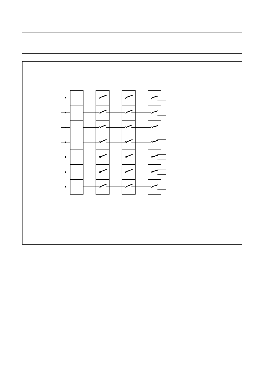
2000 Feb 23
35
Philips Semiconductors
Preliminary specification
Enhanced TV microcontrollers with
On-Screen Display (OSD)
SAA55xx
Fig.12 Interrupt structure.
handbook, full pagewidth
MBK959
priority
control
SFR IP<0:6>
global
enable
SFR IE.7
L1
H1
highest priority level 0
highest priority level 1
L2
H2
L3
EX0
H3
L4
H4
L5
H5
L6
H6
source
enable
SFR IE<0:6>
interrupt
source
L7
H7
lowest priority level 0
lowest priority level 1
ET0
EX1
ET1
ECC
ES2
EBUSY

2000 Feb 23
36
Philips Semiconductors
Preliminary specification
Enhanced TV microcontrollers with
On-Screen Display (OSD)
SAA55xx
13 TIMER/COUNTER
Two 16-bit timers/counters are incorporated Timer 0 and
Timer 1. Both can be configured to operate as either timers
or event counters.
In Timer mode, the register is incremented on every
machine cycle. It is therefore counting machine cycles.
Since the machine cycle consists of 12 oscillator periods,
the count rate is
1
/
12
f
osc
= 1 MHz.
In Counter mode, the register is incremented in response
to a negative transition at its corresponding external pin
T0 or T1. Since the pins T0 and T1 are sampled once per
machine cycle it takes two machine cycles to recognise a
transition, this gives a maximum count rate of
1
/
24
f
osc
= 0.5 MHz.
There are six Special Function Registers used to control
the timers/counters. These are: TCON, TMOD, TL0, TH0,
TL1 and TH1.
The Timer/Counter function is selected by control bits C/T
in the Timer Mode SFR(TMOD). These two
Timer/Counters have four operating modes, which are
selected by bit-pairs (M1 and M0) in TMOD. Detail of the
modes of operation is given in
"Handbook IC20,
80C51-Based 8-bit Microcontrollers".
TL0 and TH0 are the actual Timer/Counter registers for
Timer 0. TL0 is the low byte and TH0 is the high byte. TL1
and TH1 are the actual Timer/Counter registers for
Timer 1. TL1 is the low byte and TH1 is the high byte.
14 WATCHDOG TIMER
The Watchdog Timer is a counter that once in an overflow
state forces the microcontroller into a reset condition.
The purpose of the Watchdog Timer is to reset the
microcontroller if it enters an erroneous processor state
(possibly caused by electrical noise or RFI) within a
reasonable period of time. When enabled, the Watchdog
circuitry will generate a system reset if the user program
fails to reload the Watchdog Timer within a specified length
of time known as the Watchdog Interval (WI).
The Watchdog Timer consists of an 8-bit counter with an
11-bit prescaler. The prescaler is fed with a signal whose
frequency is
1
/
12
f
osc
(1 MHz for 12 MHz oscillator).
The 8-bit timer is incremented every `t' seconds where:
14.1
Watchdog Timer operation
The Watchdog operation is activated when the WLE bit in
the Power Control SFR (PCON) is set. The Watchdog can
be disabled by software by loading the value 55H into the
Watchdog Timer Key SFR (WDTKEY). This must be
performed before entering Idle/Power-down mode to
prevent exiting the mode prematurely.
Once activated the Watchdog Timer SFR (WDT) must be
reloaded before the timer overflows. The WLE bit must be
set to enable loading of the WDT SFR, once loaded the
WLE bit is reset by hardware, this is to prevent erroneous
software from loading the WDT SFR.
The value loaded into the WDT defines the Watchdog
Interval (WI).
The range of intervals is from WDT = 00H which gives
524 ms to WDT = FFH which gives 2.048 ms.
15 PULSE WIDTH MODULATORS
The device has eight 6-bit Pulse Width Modulated (PWM)
outputs for analog control of e.g. volume, balance, bass,
treble, brightness, contrast, hue and saturation. The PWM
outputs generate pulse patterns with a repetition rate of
21.33
µ
s, with the high time equal to the PWM SFR value
multiplied by 0.33
µ
s. The analog value is determined by
the ratio of the high time to the repetition time, a DC
voltage proportional to the PWM setting is obtained by
means of an external integration network (low-pass filter).
15.1
PWM control
The relevant PWM is enabled by setting the PWM enable
bit PWxE in the PWMx Control Register (where x = 0 to 7).
The high time is defined by the value PWxV<5:0>.
t
12
2048
1
f
osc
---------
◊
◊
12
2048
1
12
10
6
◊
----------------------
◊
◊
2.048 ms
=
=
=
WI
256
WDT
≠
(
)
t
◊
256
WDT
≠
(
)
2.048 ms
◊
=
=

2000 Feb 23
37
Philips Semiconductors
Preliminary specification
Enhanced TV microcontrollers with
On-Screen Display (OSD)
SAA55xx
15.2
Tuning Pulse Width Modulator (TPWM)
The device has a single 14-bit PWM that can be used for
Voltage Synthesis Tuning. The method of operation is
similar to the normal PWM except that the repetition period
is 42.66
µ
s.
15.2.1
TPWM
CONTROL
Two SFRs are used to control the TPWM, they are TDACL
and TDACH. The TPWM is enabled by setting the TPWE
bit in the TDACH SFR. The most significant bits TD<13:7>
alter the high period between 0 and 42.33
µ
s. The 7 least
significant bits TD<6:0> extend certain pulses by a further
0.33
µ
s. e.g. if TD<6:0> = 01H then 1 in 128 periods will
be extended by 0.33
µ
s, if TD<6:0> = 02H then
2 in 128 periods will be extended.
The TPWM will not start to output a new value until TDACH
has been written to. Therefore, if the value is to be
changed, TDACL should be written before TDACH.
15.3
Software ADC (SAD)
Four successive approximation Analog-to-Digital
Converters can be implemented in software by making use
of the on-board 8-bit Digital-to-Analog Converter and
Analog Comparator.
15.3.1
SAD
CONTROL
The control of the required analog input is done using the
channel select bits CH<1:0> in the SAD SFR, this selects
the required analog input to be passed to one of the inputs
of the comparator. The second comparator input is
generated by the DAC whose value is set by the bits
SAD<7:0> in the SAD and SADB SFRs. A comparison
between the two inputs is made when the start compare
bit ST in the SAD SFR is set, this must be at least one
instruction cycle after the SAD<7:0> value has been set.
The result of the comparison is given on VHI one
instruction cycle after the setting of ST.
15.3.2
SAD
INPUT VOLTAGE
The external analog voltage that is used for comparison
with the internally generated DAC voltage does not have
the same voltage range. The DAC has a lower reference
level of V
SSA
and an upper reference level of V
SSP
.
The resolution of the DAC voltage with a nominal value is
3.3
/
256
13 mV. The external analog voltage has a lower
value equivalent to V
SSA
and an upper value equivalent to
V
DDP
-
V
tn
, where V
tn
is the threshold voltage for an
NMOS transistor. The reason for this is that the input pins
for the analog signals (P3.0 to P3.3) are 5 V tolerant for
normal port operations, i.e. when not used as analog input.
To protect the analog multiplexer and comparator circuitry
from the 5 V, a series transistor is used to limit the voltage.
This limiting introduces a voltage drop equivalent to V
tn
(
0.6 V) on the input voltage. The maximum value of V
in
is
0.75 V, therefore for worst case calculations, the
maximum input to the SAD should be calculated as
V
DD(min)
=
-
0.75 V. Therefore, for an input voltage in the
range V
DDP
to V
DDP
-
V
tn
the SAD returns the same
comparison value.
15.3.3
SAD DC C
OMPARATOR MODE
The SAD module incorporates a DC Comparator mode
which is selected using the DC_COMP control bit in the
SADB SFR. This mode enables the microcontroller to
detect a threshold crossing at the input to the selected
analog input pin (P3.0/ADC0, P3.1/ADC1, P3.2/ADC2 or
P3.3/ADC3) of the software ADC. A level sensitive
interrupt is generated when the analog input voltage level
at the pin falls below the analog output level of the SAD
DAC.
This mode is intended to provide the device with a
wake-up mechanism from Power-down or Idle mode when
a key-press on the front panel of the TV is detected.
The following software sequence should be used when
utilizing this mode for Power-down or Idle mode:
1. Disable INT1 using the IE SFR.
2. Set INT1 to level sensitive using the TCON SFR.
3. Set the DAC digital input level to the desired threshold
level using SAD/SADB SFRs and select the required
input pin (P3.0/ADC0, P3.1/ADC1, P3.2/ADC2 or
P3.3/ADC3) using CH<1:0> in the SAD SFR.
4. Enter DC Compare mode by setting the DC_COMP
enable bit in the SADB SFR.
5. Enable INT1 using the IE SFR.
6. Enter Power-down/Idle mode. Upon wake-up the SAD
should be restored to its conventional operating mode
by disabling the DC_COMP control bit.
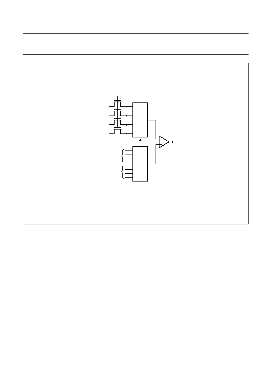
2000 Feb 23
38
Philips Semiconductors
Preliminary specification
Enhanced TV microcontrollers with
On-Screen Display (OSD)
SAA55xx
Fig.13 SAD block diagram.
handbook, halfpage
MBK960
MUX
4 : 1
ADC0
ADC1
ADC2
ADC3
CH<1:0>
SAD<3:0>
SADB<3:0>
VDDP
VHI
8-BIT
DAC

2000 Feb 23
39
Philips Semiconductors
Preliminary specification
Enhanced TV microcontrollers with
On-Screen Display (OSD)
SAA55xx
16 I
2
C-BUS SERIAL I/O
The I
2
C-bus consists of a serial data line (SDA) and a
serial clock line (SCL). The definition of the I
2
C-bus
protocol can be found in Reference 2.
The device operates in four modes
∑
Master transmitter
∑
Master receiver
∑
Slave transmitter
∑
Slave receiver.
The microcontroller peripheral is controlled by the Serial
Control SFR (S1CON) and its status is indicated by the
Status SFR (S1STA). Information is transmitted/received
to/from the I
2
C-bus using the Data SFR (S1DAT) and the
Slave Address SFR (S1ADR) is used to configure the
slave address of the peripheral.
The byte level I
2
C-bus serial port is identical to the I
2
C-bus
serial port on the P8xC558, except for the clock rate
selection bits CR<2:0>. The operation of the subsystem is
described in detail in the
"P8xC558 data sheet".
16.1
I
2
C-bus port selection
Two I
2
C-bus ports are available SCL0/SDA0 and
SCL1/SDA1. The selection of the port is done using
TXT21.I
2
C PORT 0 and TXT21.I
2
C PORT 1. When the
port is enabled, any information transmitted from the
device goes onto the enabled port. Any information
transmitted to the device can only be acted on if the port is
enabled.
If both ports are enabled then data transmitted from the
device is seen on both ports, however data transmitted to
the device on one port can not be seen on the other port.
17 MEMORY INTERFACE
The memory interface controls access to the embedded
DRAM, refreshing of the DRAM and page clearing.
The DRAM is shared between Data Capture, display and
microcontroller sections.
The Data Capture section uses the DRAM to store
acquired information that has been requested. The display
reads from the DRAM information and converts it into RGB
values. The microcontroller uses the DRAM as embedded
auxiliary RAM.
17.1
Memory structure
The memory is partitioned into two distinct areas, the
dedicated Auxiliary RAM area, and the Display RAM area.
The Display RAM area when not being used for Data
Capture or display can be used as an extension to the
Auxiliary RAM area.
17.1.1
A
UXILIARY
RAM
The Auxiliary RAM is not initialized at power-up.
The application software must initialize this Auxiliary RAM.
The contents of the Auxiliary RAM are maintained during
Idle mode, but are lost if Power-down mode is entered.
17.1.2
D
ISPLAY
RAM
The Display RAM is initialised on power-up to a value of
20H throughout. The contents of the Display RAM are
maintained when entering Idle mode. If Idle mode is exited
using an interrupt then the contents are unchanged, if Idle
mode is exited using a RESET then the contents are
initialised to 20H.
Full Closed Caption display requires display RAM from
8000H to 845FH. The memory from 846H to 84FFH (must
be initialized by the application software) can be utilized as
an extension to the dedicated contiguous Auxiliary RAM
that occupies 0000H to 07FFH.
17.2
Memory mapping
The dedicated Auxiliary RAM area occupies 2 kbytes, with
an address range from 0000H to 07FFH. The Display
RAM occupies a maximum of 10 kbytes with an address
range from 2000H to 47FFH for TXT mode and
8000H to 84FFH for CC mode (see Fig.14). The two
modes although having different address ranges occupy
physically the same DRAM area.
17.3
Addressing memory
The memory can be addressed by the microcontroller in
two ways, either directly using a MOVX command, or via
Special Function Registers depending on what address is
required.
The dedicated Auxiliary RAM, and Display memory in the
range 8000H to 84FFH, can only be accessed using the
MOVX command.
The Display memory in the range 2000H to 47FFH can
either be directly accessed using the MOVX, or via the
Special Function Registers.
2000 Feb 23
40
Philips Semiconductors
Preliminary specification
Enhanced TV microcontrollers with
On-Screen Display (OSD)
SAA55xx
17.3.1
TXT
DISPLAY MEMORY
SFR
ACCESS
The Display memory when in TXT mode (see Fig.15) is
configured as 40 columns wide by 25 rows and occupies
1K
◊
8-bit of memory. Using TXT15.BLOCK<3:0>, the
required display page can be selected to be written to.
The row and column within that block is selected using
TXT9.R<4:0> and TXT10.C<5:0>. The data at the
selected position can be read or written using
TXT11.D<7:0>.
Whenever a read or write is performed on TXT11, the row
values stored in TXT9 and column value stored in TXT10
are automatically incremented. For rows 0 to 24 the
column value is incremented up to a maximum of 39, at
which point it resets to zero and increments the row
counter value. When row 25 column 23 is reached the
values of the row and column are both reset to zero.
Writing values outside of the valid range for TXT9 or
TXT10 will cause undetermined operation of the
auto-incrementing function for accesses to TXT11.
17.3.2
TXT D
ISPLAY MEMORY
MOVX
ACCESS
It is important for the generation of OSD displays, that use
this mode of access, to understand the mapping of the
MOVX address onto the display row and column value.
This mapping of row and column onto address is shown in
Table 12. The values shown are added onto a base
address for the required memory block (see Fig.14) to give
a 16-bit address.
Table 12 Column and row to `MOVX' address (lower 10 bits of address)
ROW
COL.0
.....
COL.23
.....
COL.31
COL.32
.....
COL.39
Row 0
000H
.....
017H
.....
01FH
3F8H
.....
3FFH
Row 1
020H
.....
037H
.....
03FH
3F0H
.....
3F7H
:
:
:
:
:
:
:
:
:
:
:
:
:
:
:
:
:
:
Row 23
2E0H
.....
3F7H
.....
2FFH
340H
.....
347H
Row 24
300H
.....
317H
.....
31FH
338H
.....
33FH
Row 25
320H
.....
337H

2000 Feb 23
41
Philips Semiconductors
Preliminary specification
Enhanced TV microcontrollers with
On-Screen Display (OSD)
SAA55xx
handbook, halfpage
GSA085
upper 32 kbytes
lower 32 kbytes
TXT BLOCK 0
0000H
2000H
TXT BLOCK 9
2400H
TXT BLOCK 1
2800H
TXT BLOCK 2
2C00H
TXT BLOCK 3
3000H
TXT BLOCK 4
3400H
TXT BLOCK 5
3800H
TXT BLOCK 6
3C00H
TXT BLOCK 7
4000H
TXT BLOCK 8
4400H
7FFFH
CC DISPLAY
8000H
84FFH
FFFFH
AUXILIARY
07FFH
Fig.14 DRAM memory mapping.
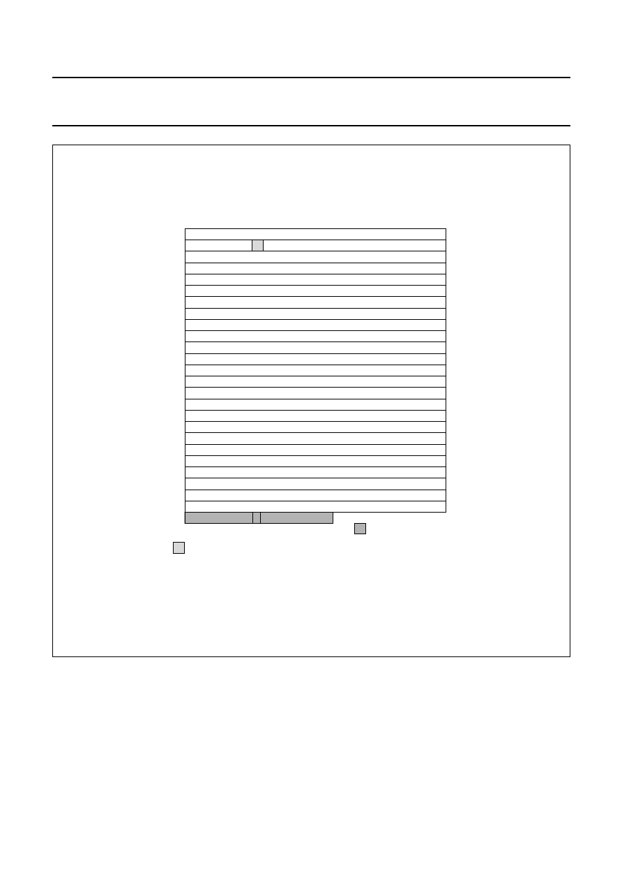
2000 Feb 23
42
Philips Semiconductors
Preliminary specification
Enhanced TV microcontrollers with
On-Screen Display (OSD)
SAA55xx
Fig.15 TXT memory map.
handbook, full pagewidth
0
20
30
10
C
9
0
23
39
Column
10
MBK962
control data
active position TXT9.R<4:0> = 01H, TXT10.C<5:0> = 0AH, TXT11 = 43H
non-displayable data
(byte 10 reserved)
Row 0
1
2
3
4
5
6
7
8
9
10
11
12
13
14
15
16
17
18
19
20
21
22
23
24
25

2000 Feb 23
43
Philips Semiconductors
Preliminary specification
Enhanced TV microcontrollers with
On-Screen Display (OSD)
SAA55xx
17.4
Page clearing
Page clearing is performed on request from either the Data
Capture block, or the microcontroller under the control of
the embedded software.
At power-on and reset the whole of the page memory is
cleared. The TXT13.PAGE CLEARING bit will be set while
this takes place.
17.4.1
D
ATA
C
APTURE PAGE CLEAR
When a page header is acquired for the first time after a
new page request or a page header is acquired with the
erase (C4) bit set the page memory is `cleared' to spaces
before the rest of the page arrives.
When this occurs, the space code (20H) is written into
every location of rows 1 to 23 of the basic page memory,
the appropriate packet 27 row of the extension packet
memory and the row where teletext packet 24 is written.
This last row is either row 24 of the basic page memory, if
the TXT0.X24 POSN bit is set, or row 0 of the extension
packet memory, if the bit is not set. Page clearing takes
place before the end of the TV line in which the header
arrived which initiated the page clear.
This means that the 1 field gap between the page header
and the rest of the page which is necessary for many
teletext decoders is not required.
17.4.2
S
OFTWARE PAGE CLEAR
The software can also initiate a page clear, by setting the
TXT9.CLEAR MEMORY bit. When it does so, every
location in the memory block pointed to by
TXT15.BLOCK<3:0> is cleared to a space code (20H).
The CLEAR MEMORY bit is not latched so the software
does not have to reset it after it has been set.
Only one page can be cleared in a TV line so if the
software requests a page clear it will be carried out on the
next TV line on which the Data Capture hardware does not
force the page to be cleared. A flag, TXT13.PAGE
CLEARING, is provided to indicate that a software
requested page clear is being carried out. The flag is set
when a logic 1 is written into the TXT9.CLEAR MEMORY
bit and is reset when the page clear has been completed.
If TXT0.INV ON bit = 1 and a page clear is initiated on
Block 8 all locations are cleared to 00H.
18 DATA CAPTURE
The Data Capture section takes in the analog Composite
Video and Blanking Signal (CVBS), and from this extracts
the required data, which is then decoded and stored in
memory.
The extraction of the data is performed in the digital
domain. The first stage is to convert the analog CVBS
signal into a digital form. This is done using an ADC
sampling at 12 MHz. The data and clock recovery is then
performed by a Multi-rate Video Input Processor (MulVIP).
From the recovered data and clock the following data
types are extracted WST Teletext (625/525), Closed
Caption, VPS and WSS. The extracted data is stored in
either memory (DRAM) via the Memory interface or in SFR
locations.
18.1
Data Capture features
∑
Two CVBS inputs
∑
Video Signal Quality detector
∑
Data Capture for 625-line WST
∑
Data Capture for 525-line WST
∑
Data Capture for US Closed Caption
∑
Data Capture for VPS data (PDC system A)
∑
Data Capture for Wide Screen Signalling (WSS) bit
decoding
∑
Automatic selection between 525 WST/625 WST
∑
Automatic selection between 625 WST/VPS on
line 16 of Vertical Blanking Interval
∑
Real-time capture and decoding for WST Teletext in
hardware, to enable optimized microprocessor
throughput
∑
Up to 10 pages stored on-chip
∑
Inventory of transmitted Teletext pages stored in the
Transmitted Page Table (TPT) and Subtitle Page Table
(SPT)
∑
Automatic detection of FASTEXT transmission
∑
Real-time packet 26 engine in hardware for processing
accented, G2 and G3 characters
∑
Signal quality detector for WST/VPS data types
∑
Comprehensive Teletext language coverage
∑
Full Field and Vertical Blanking Interval (VBI) data
capture of WST data.
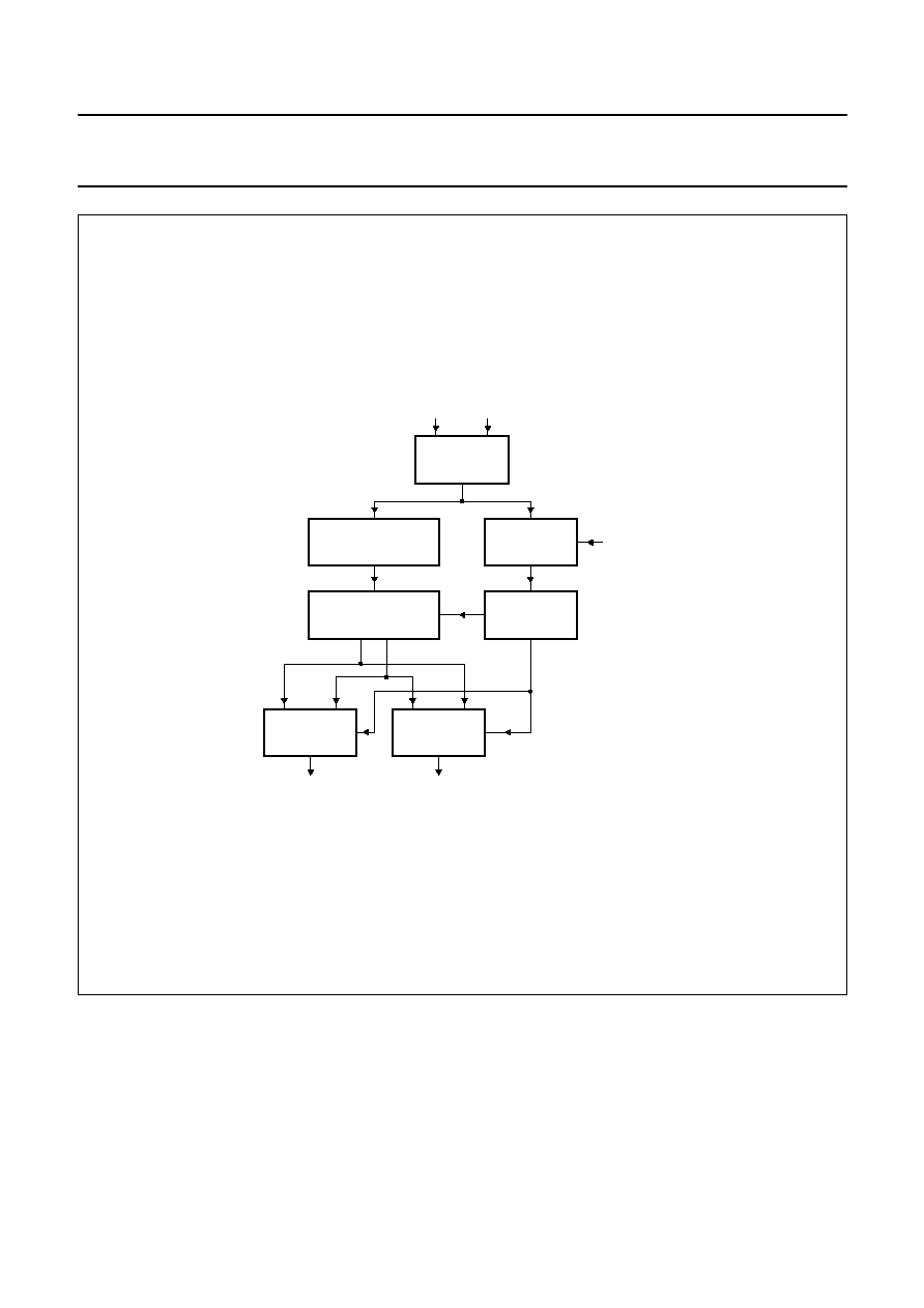
2000 Feb 23
44
Philips Semiconductors
Preliminary specification
Enhanced TV microcontrollers with
On-Screen Display (OSD)
SAA55xx
Fig.16 Data capture block diagram.
handbook, full pagewidth
ADC
data<7:0>
VCS
SYNC_FILTER
TTD
TTC
DATA SLICER
AND
CLOCK RECOVERY
output data to
memory interface
output data to SFRs
MBK963
ACQUISITION
FOR
WST/VPS
ACQUISITION
FOR
CC/WSS
CVBS
SWITCH
CVBS
CVBS0
CVBS1
ACQUISITION
TIMING
SYNC
SEPARATOR

2000 Feb 23
45
Philips Semiconductors
Preliminary specification
Enhanced TV microcontrollers with
On-Screen Display (OSD)
SAA55xx
18.1.1
CVBS S
WITCH
The CVBS switch is used to select the required analog
input depending on the value of TXT8.CVBS1/CVBS0.
18.1.2
A
NALOG
-
TO
-D
IGITAL
C
ONVERTER
The output of the CVBS switch is passed to a
Differential-to-Single-Ended Converter (DIVIS), although
in this device it is used in single-ended configuration with
a reference. The analog output of the DIVIS is converted
into a digital representation by a full-flash ADC with a
sampling rate of 12 MHz.
18.1.3
M
ULTI
-
RATE VIDEO INPUT PROCESSOR
The multi-rate video input processor is a Digital Signal
Processor designed to extract the data and recover the
clock from a digitized CVBS signal.
18.1.4
D
ATA STANDARDS
The data and clock standards that can be recovered are
shown in Table 13.
Table 13 Data Slicing standards
18.1.5
D
ATA
C
APTURE TIMING
The Data Capture timing section uses the synchronisation
information extracted from the CVBS signal to generate
the required horizontal and vertical reference timings.
The timing section automatically recognizes and selects
the appropriate timings for either 625 (50 Hz)
synchronisation or 525 (60 Hz) synchronisation.
A flag TXT12.VIDEO SIGNAL QUALITY is set when the
timing section is locked correctly to the incoming CVBS
signal. When TXT12.VIDEO SIGNAL QUALITY is set
another flag TXT12.525/625 SYNC can be used to identify
the standard.
18.1.6
A
CQUISITION
The acquisition sections extracts the relevant information
from the serial stream of data from the MulVIP and stores
it in memory.
18.1.6.1
Making a page request
A page is requested by writing a series of bytes into the
TXT3.PRD<4:0> SFR which corresponds to the number of
the page required. The bytes written into TXT3 are stored
in a RAM with an auto-incrementing address. The start
address for the RAM is set using the TXT2.SC<2:0> to
define which part of the page request is being written, and
TXT2.REQ<3:0> is used to define which of the 10 page
requests is being modified. If TXT2.REQ<3:0> is greater
than 09H, then data being written to TXT3 is ignored.
Table 14 shows the contents of the page request RAM.
Up to 10 pages of teletext can be acquired on the 10 page
device, when TXT1.EXT PKT OFF is set to logic 1, and up
to 9 pages can be acquired when this bit is set to logic 0.
For a 20 page device the 10 page acquisition channels are
banked, the bank being selected using TXT2.ACQ BANK.
If the `Do Care' bit for part of the page number is set logic 0
then that part of the page number is ignored when the
teletext decoder is deciding whether a page being
received off air should be stored or not. For example, if the
Do Care bits for the four subcode digits are all set to logic 0
then every subcode version of the page will be captured.
Table 14 The contents of the Page request RAM
DATA STANDARD
CLOCK RATE
625 WST
6.9375 MHz
525 WST
5.7272 MHz
VPS
5.0 MHz
WSS
5.0 MHz
Closed Caption
500 kHz
START
COLUMN
PRD4
PRD3
PRD2
PRD1
PRD0
0
DO CARE
Magazine
HOLD MAG2 MAG1 MAG0
1
DO CARE
Page Tens
PT3
PT2
PT1
PT0
2
DO CARE
Page
Units
PU3
PU2
PU1
PU0
3
DO CARE
Hour Tens
X
X
HT1
HT0
4
DO CARE
Hours
Units
HU3
HU2
HU1
HU0
5
DO CARE
Minutes
Tens
X
MT2
MT1
MT0
6
DO CARE
Minutes
Units
MU3
MU2
MU1
MU0
7
X
X
X
E1
E0

2000 Feb 23
46
Philips Semiconductors
Preliminary specification
Enhanced TV microcontrollers with
On-Screen Display (OSD)
SAA55xx
When the HOLD bit is set to a logic 0 the teletext decoder
will not recognise any page as having the correct page
number and no pages will be captured. In addition to
providing the user requested hold function this bit should
be used to prevent the inadvertent capture of an unwanted
page when a new page request is being made.
For example, if the previous page request was for
page 100 and this was being changed to page 234, it
would be possible to capture page 200 if this arrived after
only the requested magazine number had been changed.
The E1 and E0 bits control the error checking which should
be carried out on packets 1 to 23 when the page being
requested is captured. This is described in more detail in
Section 18.1.6.3.
For a multi-page device, each packet can only be written
into one place in the teletext RAM so if a page matches
more than one of the page requests the data is written into
the area of memory corresponding to the lowest numbered
matching page request.
At power-up each page request defaults to any page, hold
on and error check Mode 0.
18.1.6.2
Rolling headers and time
When a new page has been requested it is conventional
for the decoder to turn the header row of the display green
and to display each page header as it arrives until the
correct page has been found.
When a page request is changed (i.e. when the TXT3 SFR
is written to) a flag (PBLF) is written into bit 5, column 9,
row 25 of the corresponding block of the page memory.
The state of the flag for each block is updated every TV
line, if it is set for the current display block, the acquisition
section writes all valid page headers which arrive into the
display block and automatically writes an alphanumeric
green character into column 7 of row 0 of the display block
every TV line.
When a requested page header is acquired for the first
time, rows 1 to 23 of the relevant memory block are
cleared to space, i.e. have 20H written into every column,
before the rest of the page arrives. Row 24 is also cleared
if the TXT0.X24 POSN bit is set. If the
TXT1.EXT PKT OFF bit is set the extension packets
corresponding to the page are also cleared.
The last 8 characters of the page header are used to
provide a time display and are always extracted from every
valid page header as it arrives and written into the display
block.
The TXT0.DISABLE HEADER ROLL bit prevents any data
being written into row 0 of the page memory except when
a page is acquired off air i.e. rolling headers and time are
not written into the memory. The TXT1.ACQ OFF bit
prevents any data being written into the memory by the
teletext acquisition section.
When a parallel magazine mode transmission is being
received only headers in the magazine of the page
requested are considered valid for the purposes of rolling
headers and time. Only one magazine is used even if don't
care magazine is requested. When a serial magazine
mode transmission is being received all page headers are
considered to be valid.
18.1.6.3
Error checking
Before teletext packets are written into the page memory
they are error checked. The error checking carried out
depends on the packet number, the byte number, the error
check mode bits in the page request data and the
TXT1.8-BIT bit.
If an uncorrectable error occurs in one of the Hamming
checked addressing and control bytes in the page header
or in the Hamming checked bytes in packet 8/30, bit 4 of
the byte written into the memory is set, to act as an error
flag to the software. If uncorrectable errors are detected in
any other Hamming checked data the byte is not written
into the memory.
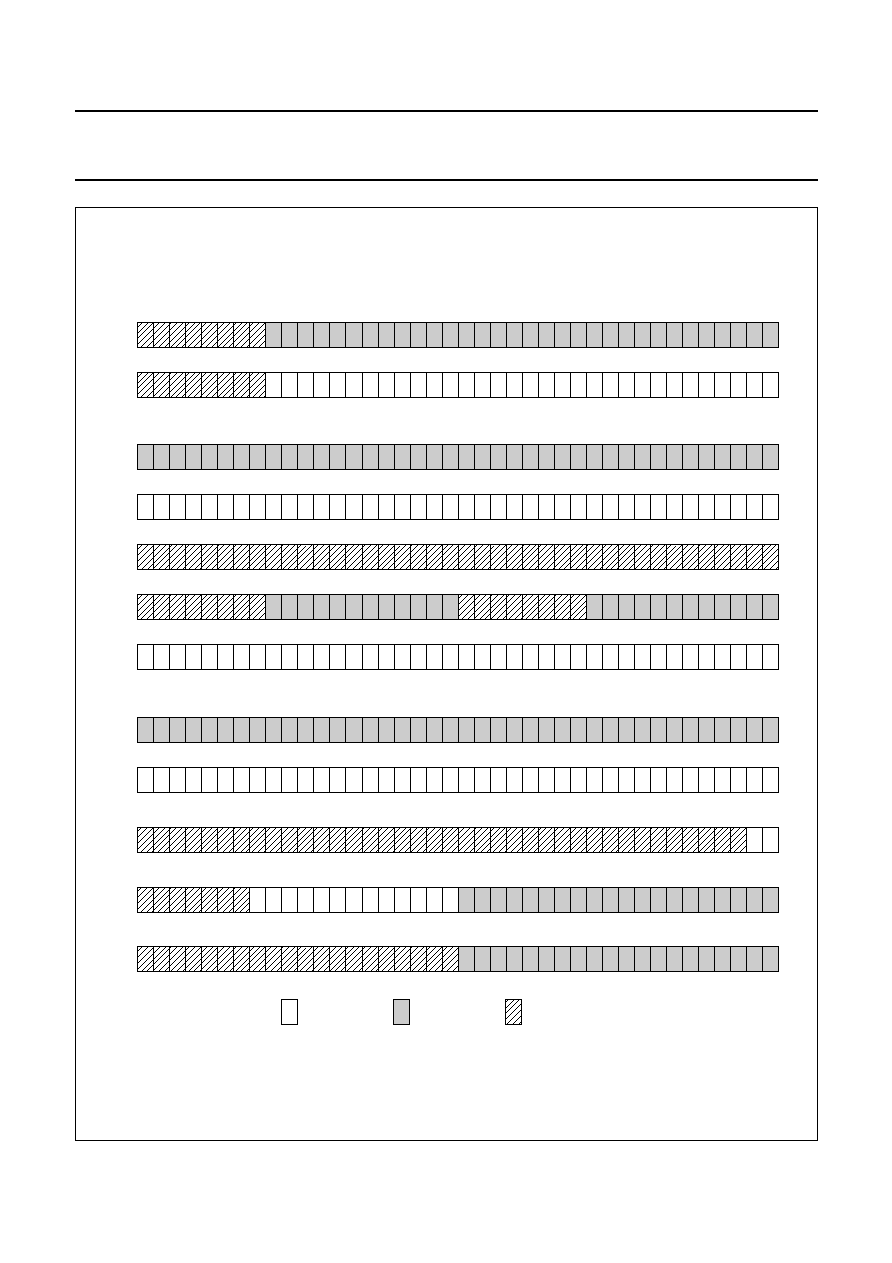
2000 Feb 23
47
Philips Semiconductors
Preliminary specification
Enhanced TV microcontrollers with
On-Screen Display (OSD)
SAA55xx
Fig.17 Error checking.
handbook, full pagewidth
MGK465
39
38
37
36
35
34
33
32
31
30
29
28
27
26
25
24
23
22
21
20
19
18
17
16
15
14
13
12
11
10
9
8
7
6
5
4
3
2
1
0
'8-bit' bit = 0
39
38
37
36
35
34
33
32
31
30
29
28
27
26
25
24
23
22
21
20
19
18
17
16
15
14
13
12
11
10
9
8
7
6
5
4
3
2
1
0
'8-bit' bit = 1
Packet X/0
39
38
37
36
35
34
33
32
31
30
29
28
27
26
25
24
23
22
21
20
19
18
17
16
15
14
13
12
11
10
9
8
7
6
5
4
3
2
1
0
'8-bit' bit = 0, error check mode = 0
39
38
37
36
35
34
33
32
31
30
29
28
27
26
25
24
23
22
21
20
19
18
17
16
15
14
13
12
11
10
9
8
7
6
5
4
3
2
1
0
'8-bit' bit = 0, error check mode = 1
39
38
37
36
35
34
33
32
31
30
29
28
27
26
25
24
23
22
21
20
19
18
17
16
15
14
13
12
11
10
9
8
7
6
5
4
3
2
1
0
'8-bit' bit = 0, error check mode = 2
39
38
37
36
35
34
33
32
31
30
29
28
27
26
25
24
23
22
21
20
19
18
17
16
15
14
13
12
11
10
9
8
7
6
5
4
3
2
1
0
'8-bit' bit = 0, error check mode = 3
39
38
37
36
35
34
33
32
31
30
29
28
27
26
25
24
23
22
21
20
19
18
17
16
15
14
13
12
11
10
9
8
7
6
5
4
3
2
1
0
'8-bit' bit = 1
Packet X/1-23
39
38
37
36
35
34
33
32
31
30
29
28
27
26
25
24
23
22
21
20
19
18
17
16
15
14
13
12
11
10
9
8
7
6
5
4
3
2
1
0
'8-bit' bit = 0
39
38
37
36
35
34
33
32
31
30
29
28
27
26
25
24
23
22
21
20
19
18
17
16
15
14
13
12
11
10
9
8
7
6
5
4
3
2
1
0
'8-bit' bit = 1
Packet X/24
39
38
37
36
35
34
33
32
31
30
29
28
27
26
25
24
23
22
21
20
19
18
17
16
15
14
13
12
11
10
9
8
7
6
5
4
3
2
1
0
Packet X/27/0
39
38
37
36
35
34
33
32
31
30
29
28
27
26
25
24
23
22
21
20
19
18
17
16
15
14
13
12
11
10
9
8
7
6
5
4
3
2
1
0
Packet 8/30/0,1
39
38
37
36
35
34
33
32
31
30
29
28
27
26
25
24
23
22
21
20
19
18
17
16
15
14
13
12
11
10
9
8
7
6
5
4
3
2
1
0
8-bit
data
Packet 8/30/2,3,4-15
odd parity
checked
8/4 Hamming
checked

2000 Feb 23
48
Philips Semiconductors
Preliminary specification
Enhanced TV microcontrollers with
On-Screen Display (OSD)
SAA55xx
Fig.18 Packet storage locations.
(1) If `X24 POSN' bit = 1.
(2) VPS data block 9, unused in blocks 0 to 8.
(3) Byte 10 reserved.
handbook, full pagewidth
Row 0
1
2
3
4
5
6
7
8
9
10
11
12
13
14
15
16
17
18
19
20
21
22
23
24
25
0
6
7
8
9
0
23
39
Packet X/0
Basic Page Blocks (0 to 8/9)
OSD only
Packet X/1
Packet X/2
Packet X/3
Packet X/4
Packet X/5
Packet X/6
Packet X/7
Packet X/8
Packet X/9
Packet X/10
Packet X/11
Packet X/12
Packet X/13
Packet X/14
Packet X/15
Packet X/16
Packet X/17
Packet X/18
Packet X/19
Packet X/20
Packet X/21
Packet X/22
Packet X/23
Packet X/24
(1)
GSA003
Control Data
VPS Data
(2)
10
(3)

2000 Feb 23
49
Philips Semiconductors
Preliminary specification
Enhanced TV microcontrollers with
On-Screen Display (OSD)
SAA55xx
18.1.6.4
Teletext memory organisation
The teletext memory is divided into 2 banks of 10 blocks.
Normally, when the TXT1.EXT PKT OFF bit is logic 0,
each of blocks 0 to 8 contains a teletext page arranged in
the same way as the basic page memory of the page
device and block 9 contains extension packets. When the
TXT1.EXT PKT OFF bit is logic 1, no extension packets
are captured and block 9 of the memory is used to store
another page. The number of the memory block into which
a page is written corresponds to the page request number
which resulted in the capture of the page.
Packet 0, the page header, is split into two parts when it is
written into the text memory. The first 8 bytes of the header
contain control and addressing information. They are
Hamming decoded and written into columns 0 to 7 of
row 25. Row 25 also contains the magazine number of the
acquired page and the PLBF flag but the last 14 bytes are
unused and may be used by the software, if necessary.
Fig.19 Extension packet storage locations.
(1) If `X24 POSN' bit = 0.
(2) Byte 10 reserved.
handbook, full pagewidth
GSA002
0
1
2
3
4
5
6
7
8
9
9
23
0
10
11
12
13
14
15
20
21
22
23
24
25
16
17
18
19
Row
Packet X/24 for page in block 0
(1)
Packet X/24 for page in block 1
(1)
Packet X/27/0 for page in block 0
Packet X/27/0 for page in block 1
Packet X/24 for page in block 2
(1)
Packet X/27/0 for page in block 2
Packet X/24 for page in block 3
(1)
Packet X/27/0 for page in block 3
Packet X/24 for page in block 4
(1)
Packet X/27/0 for page in block 4
Packet X/24 for page in block 5
(1)
Packet X/27/0 for page in block 5
Packet X/24 for page in block 6
(1)
Packet X/27/0 for page in block 6
Packet X/24 for page in block 7
(1)
Packet X/27/0 for page in block 7
Packet X/24 for page in block 8
(1)
Packet X/27/0 for page in block 8
Packet 8/30/0.1
Packet 8/30/2.3
Packet 8/30/4-15
VPS Data
Extension Packet Block (9)
10
(2)

2000 Feb 23
50
Philips Semiconductors
Preliminary specification
Enhanced TV microcontrollers with
On-Screen Display (OSD)
SAA55xx
18.1.6.5
Row 25 data contents
The Hamming error flags are set if the on-board 8/4
Hamming checker detects that there has been an
uncorrectable (2-bit) error in the associated byte. It is
possible for the page to still be acquired if some of the
page address information contains uncorrectable errors if
that part of the page request was a `Don't Care'. There is
no error flag for the magazine number as an uncorrectable
error in this information prevents the page being acquired.
The interrupt sequence (C9) bit is automatically dealt with
by the acquisition section so that rolling headers do not
contain a discontinuity in the page number sequence.
The magazine serial (C11) bit indicates whether the
transmission is a serial or a parallel magazine
transmission. This affects the way the acquisition section
operates and is dealt with automatically.
The newsflash (C5), subtitle (C6), suppress header (C7),
inhibit display (C10) and language control (C12 to 14) bits
are dealt with automatically by the display section.
The update (C8) bit has no effect on the hardware.
The remaining 32 bytes of the page header are parity
checked and written into columns 8 to 39 of row 0. Bytes
which pass the parity check have the MSB set to a logic 0
and are written into page memory. Bytes with parity errors
are not written into the memory.
Table 15 The data in row 25 of the basic page memory
COL
BIT 7
BIT 6
BIT 5
BIT 4
BIT 3
BIT 2
BIT 1
BIT 0
0
0
0
0
Hamming error
PU3
PU2
PU1
PU0
1
0
0
0
Hamming error
PT3
PT2
PT1
PT0
2
0
0
0
Hamming error
MU3
MU2
MU1
MU0
3
0
0
0
Hamming error
C4
MT2
MT1
MT0
4
0
0
0
Hamming error
HU3
HU2
HU1
HU0
5
0
0
0
Hamming error
C6
C5
HT1
HT0
6
0
0
0
Hamming error
C10
C9
C8
C7
7
0
0
0
Hamming error
C14
C13
C12
C11
8
0
0
0
FOUND
0
MAG2
MAG1
MAG0
9
0
0
PBLF
0
0
0
0
0
10 to 23
-
-
-
unused
-
-
-
-

2000 Feb 23
51
Philips Semiconductors
Preliminary specification
Enhanced TV microcontrollers with
On-Screen Display (OSD)
SAA55xx
18.1.6.6
Inventory page
If the TXT0.INV ON bit is a logic 1, memory block 8 is used
as an inventory page.The inventory page consists of two
tables: the Transmitted Page Table (TPT) and the Subtitle
Page Table (SPT).
In each table, every possible combination of the page tens
and units digit, 00H to FFH, is represented by a byte.
Each bit of these bytes corresponds to a magazine number
so each page number, from 100H to 8FFH, is represented
by a bit in the table.
The bit for a particular page in the TPT is set when a page
header is received for that page. The bit in the SPT is set
when a page header for the page is received which has the
`subtitle' page header control bit (C6) set. The bit for a
particular page in the TPT is set when a page header is
received for that page. The bit in the SPT is set when a
page header for the page is received which has the
`subtitle' page header control bit (C6) set.
Fig.20 Transmitted/subtitle page organisation.
handbook, full pagewidth
x00
x01
x02
x03
x04
x05
x06
x07
x08
x09
x0a
x0b
x0c
x0d
x0e
x0f
x10
x11
x12
x13
x14
x15
x16
x17
x18
x19
x1a
x1b
x1c
x1d
x1e
x1f
x20
x21
x22
x23
x24
x25
x26
x27
x28
x29
x2a
x2b
x2c
x2d
x2e
x2f
x30
x31
x32
x33
x34
x35
x36
x37
x38
x39
x3a
x3b
x3c
x3d
x3e
x3f
xc0
xc1
xc2
xc3
xc4
xc5
xc6
xc7
xc8
xc9
xca
xcb
xcc
xcd
xce
xcf
xd0
xd1
xd2
xd3
xd4
xd5
xd6
xd7
xd8
xd9
xda
xdb
xdc
xdd
xde
xdf
xe0
xe1
xe2
xe3
xe4
xe5
xe6
xe7
xe8
xe9
xea
xeb
xec
xed
xee
xfef
xf0
xf1
xf2
xf3
xf4
xf5
xf6
xf7
xf8
xf9
xfa
xfb
xfc
xfd
xfe
xff
7xx
bit
7
Bytes in the table
bits in each byte
column
row n
n + 1
n + 6
n + 7
0
0
MGD160
8
16
24
32
39
6xx
5xx
4xx
3xx
2xx
1xx
8xx

2000 Feb 23
52
Philips Semiconductors
Preliminary specification
Enhanced TV microcontrollers with
On-Screen Display (OSD)
SAA55xx
Fig.21 Inventory page organisation.
handbook, full pagewidth
MGD165
0
1
2
3
4
5
6
7
8
9
23
0
0
39
10
11
12
13
14
15
20
21
22
23
24
25
16
17
18
19
Row
Unused
Unused
Unused
Unused
Unused
Unused
Unused
Unused
Unused
Transmitted
Pages
Table
Subtitle
Pages
Table

2000 Feb 23
53
Philips Semiconductors
Preliminary specification
Enhanced TV microcontrollers with
On-Screen Display (OSD)
SAA55xx
18.1.6.7
Packet 26 processing
One of the uses of packet 26 is to transmit characters
which are not in the basic teletext character set. The family
automatically decodes packet 26 data and, if a character
corresponding to that being transmitted is available in the
character set, automatically writes the appropriate
character code into the correct location in the teletext
memory. This is not a full implementation of the packet 26
specification allowed for in level 2 teletext, and so is often
referred to as level 1.5.
By convention, the packets 26 for a page are transmitted
before the normal packets. To prevent the default
character data overwriting the packet 26 data the device
incorporates a mechanism which prevents packet 26 data
from being overwritten. The mechanism is disabled when
the Spanish national option is detected as the Spanish
transmission system sends even parity (i.e. incorrect)
characters in the basic page locations corresponding to
the characters sent via packet 26 and these will not
overwrite the packet 26 characters anyway. The special
treatment of Spanish national option is prevented if
TXT12.ROM VER R4 is logic 0 or if the TXT8.DISABLE
SPANISH is set.
Packet 26 data is processed regardless of the
TXT1.EXT PKT OFF bit, but setting theTXT1.X26 OFF
disables packet 26 processing.
The TXT8.PKT26 RECEIVED bit is set by the hardware
whenever a character is written into the page memory by
the packet 26 decoding hardware. The flag can be reset by
writing a logic 0 into the SFR bit.
18.1.6.8
525-line World System Teletext
The 525-line format is similar to the 625-line format but the
data rate is lower and there are less data bytes per packet
(32 rather than 40). There are still 40 characters per
display row so extra packets are sent each of which
contains the last 8 characters for four rows. These packets
can be identified by looking at the `tabulation bit' (T), which
replaces one of the magazine bits in 525-line teletext.
When an ordinary packet with T = 1 is received, the
decoder puts the data into the four rows starting with that
corresponding to the packet number, but with the 2 LSBs
set to logic 0. For example, a packet 9 with T = 1
(packet X/1/9) contains data for rows 8, 9, 10 and 11.
The error checking carried out on data from packets with
T = 1 depends on the setting of the TXT1. 8-BIT bit and the
error checking control bits in the page request data and is
the same as that applied to the data written into the same
memory location in the 625-line format.
The rolling time display (the last 8 characters in row 0) is
taken from any packets X/1/1, 2 or 3 received. In parallel
magazine mode only packets in the correct magazine are
used for rolling time. Packet number X/1/0 is ignored.
The tabulation bit is also used with extension packets.
The first 8 data bytes of packet X/1/24 are used to extend
the Fastext prompt row to 40 characters. These characters
are written into whichever part of the memory the
packet 24 is being written into (determined by the
`X24 POSN' bit).
Packets X/0/27/0 contain 5 Fastext page links and the link
control byte and are captured, Hamming checked and
stored in the same way as are packets X/27/0 in 625-line
text. Packets X/1/27/0 are not captured.
Because there are only 2 magazine bits in 525-line text,
packets with the magazine bits all set to a logic 0 are
referred to as being in magazine 4. Therefore, the
broadcast service data packet is packet 4/30, rather than
packet 8/30. As in 625-line text, the first 20 bytes of
packet 4/30 contain encoded data which is decoded in the
same way as that in packet 8/30. The last 12 bytes of the
packet contains half of the parity encoded status message.
Packet 4/0/30 contains the first half of the message and
packet 4/1/30 contains the second half. The last 4 bytes of
the message are not written into memory. The first
20 bytes of the each version of the packet are the same so
they are stored whenever either version of the packet is
acquired.
In 525-line text each packet 26 only contains ten 24/18
Hamming encoded data triplets, rather than the 13 found
in 625-line text. The tabulation bit is used as an extra bit
(the MSB) of the designation code, allowing 32 packet 26s
to be transmitted for each page. The last byte of each
packet 26 is ignored.
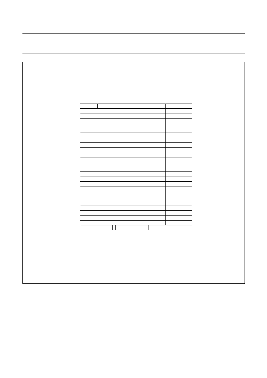
2000 Feb 23
54
Philips Semiconductors
Preliminary specification
Enhanced TV microcontrollers with
On-Screen Display (OSD)
SAA55xx
Fig.22 Packet storage locations, 525-line.
(1) If X24 POSN bit = 1.
(2) Byte 10 reserved.
handbook, full pagewidth
GSA004
Row 0
1
2
3
4
5
6
7
8
9
10
11
12
13
14
15
16
17
18
19
20
21
22
23
24
25
0
6
7
8
9
0
23
39
Packet X/0/0
OSD only
Rolling time
aw/ag
Packet X/0/1
Packet X/1/1
Packet X/0/2
Packet X/0/3
Packet X/0/4
Packet X/1/4
Packet X/0/5
Packet X/0/6
Packet X/0/7
Packet X/0/8
Packet X/1/8
Packet X/0/9
Packet X/0/10
Packet X/0/11
Packet X/0/12
Packet X/1/12
Packet X/0/13
Packet X/0/14
Packet X/0/15
Packet X/0/16
Packet X/1/16
Packet X/0/17
Packet X/0/18
Packet X/0/19
Packet X/0/20
Packet X/1/20
Packet X/0/21
Packet X/0/22
Packet X/0/23
Packet X/0/24
(1)
Packet X/1 /24
(1)
Control Data
10
(2)

2000 Feb 23
55
Philips Semiconductors
Preliminary specification
Enhanced TV microcontrollers with
On-Screen Display (OSD)
SAA55xx
18.1.6.9
Fastext detection
When a packet 27, designation code 0 is detected,
whether or not it is acquired, the TXT13.FASTEXT bit is
set. If the device is receiving 525-line teletext, a packet
X/0/27/0 is required to set the flag. The flag can be reset
by writing a logic 0 into the SFR bit.
When a packet 8/30 is detected, or a packet 4/30 when the
device is receiving a 525-line transmission, the
TXT13.PKT 8/30 is set. The flag can be reset by writing a
logic 0 into the SFR bit.
18.1.6.10 Broadcast Service Data Detection
When a packet 8/30 is detected, or a packet 4/30 when the
device is receiving a 525-line transmission, the
TXT13. PKT 8/30 flag is set. The flag can be reset by
writing a logic 0 into the SFR bit.
18.1.6.11 VPS acquisition
When the TXT0.VPS ON bit is set, any VPS data present
on line 16, field 0 of the CVBS signal at the input of the
teletext decoder is error checked and stored in row 25,
block 9 of the basic page memory. The device
automatically detects whether teletext or VPS is being
transmitted on this line and decodes the data
appropriately.
Each VPS byte in the memory consists of 4 biphase
decoded data bits (bits 0 to 3), a biphase error flag (bit 4)
and three logic 0s (bits 5 to 7).
The most significant bit of the VPS data cannot be set to
logic 1.
The TXT13.VPS RECEIVED bit is set by the hardware
whenever VPS data is acquired.
Full details of the VPS system can be found in the
specification
"Domestic Video Program Delivery Control
System (PDC); EBU Tech. 3262-E".
18.1.7
WST
ACQUISITION
The family is capable of acquiring Level 1.5 625-line and
525-line World System Teletext.
18.1.8
WSS
ACQUISITION
The Wide Screen Signalling data transmitted on line 23
gives information on the aspect ratio and display position
of the transmitted picture, the position of subtitles and on
the camera/film mode. Some additional bits are reserved
for future use. A total of 14 data bits are transmitted.
All of the available data bits transmitted by the Wide
Screen Signalling signal are captured and stored in SFRs
WSS1, WSS2 and WSS3. The bits are stored as groups of
related bits and an error flag is provided for each group to
indicate when a transmission error has been detected in
one or more of the bits in the group.
Wide screen signalling data is only acquired when the
TXT8.WSS ON bit is set.
The TXT8.WSS RECEIVED bit is set by the hardware
whenever wide screen signalling data is acquired. The flag
can be reset by writing a logic 0 into the SFR bit.
Fig.23 VPS data storage.
handbook, full pagewidth
teletext page
header data
VPS
byte 11
row 25
10
11
column
0
9
MBK964
VPS
byte 12
VPS
byte 13
VPS
byte 14
VPS
byte 15
VPS
byte 4
VPS
byte 5
12
13 14
15 16
17 18
19 20
21 22
23

2000 Feb 23
56
Philips Semiconductors
Preliminary specification
Enhanced TV microcontrollers with
On-Screen Display (OSD)
SAA55xx
18.1.9
C
LOSED
C
APTION ACQUISITION
The US Closed Caption data is transmitted on line 21
(525-line timings) and is used for Captioning information,
Text information and Extended Data Services. Full details
can be found in the document
"Recommended Practise for
Line 21 Data Service EIA-608".
Closed Caption data is only acquired when TXT21.CC ON
bit is set.
Two bytes of data are stored per field in SFRs the first bye
is stored in CCDAT1 and the second byte is stored in
CCDAT2. The value in the CCDAT registers are reset to
00H at the start of the Closed Caption line defined by
CCLIN.CS<4:0>. At the end of the Closed Caption line an
interrupt is generated if IE.ECC is active.
The processing of the Closed Caption data to convert into
a displayable format is performed by software.
19 DISPLAY
The display section is based on the requirements for a
Level 1.5 WST Teletext and US Closed Caption. There are
some enhancements for use with locally generated
On-Screen Displays.
The display section reads the contents of the Display
memory and interprets the control/character codes.
From this information and other global settings, the display
produces the required RGB signals and Video/Data (Fast
Blanking) signal for a TV signal processing device.
The display is synchronized to the TV signal processing
device by way of horizontal and vertical sync signals
provided by external circuits (Slave Sync mode). From
these signals all display timings are derived.
19.1
Display features
∑
Teletext and Enhanced OSD modes
∑
Level 1.5 WST features
∑
US Closed Caption features
∑
Serial and Parallel display attributes
∑
Single/double/quadruple width and height for characters
∑
Scrolling of display region
∑
Variable flash rate controlled by software
∑
Globally selectable scan lines per row 9/10/13/16
∑
Globally selectable character matrix (H
◊
V) 12
◊
9,
12
◊
10, 12
◊
13 or 12
◊
16
∑
Italics
∑
Soft colours using CLUT with 4096 colour palette
∑
Underline
∑
Overline
∑
Fringing (shadow) selectable from N-S-E-W direction
∑
Fringe colour selectable
∑
Meshing of defined area
∑
Contrast reduction of defined area
∑
Cursor
∑
Special graphics characters with two planes, allowing
four colours per character
∑
32 software redefinable On-Screen Display characters
∑
4 WST character sets (G0/G2) in single device
(e.g. Latin, Cyrillic, Greek and Arabic)
∑
G1 Mosaic graphics, Limited G3 Line drawing
characters
∑
WST character sets and Closed Caption character set in
single device.
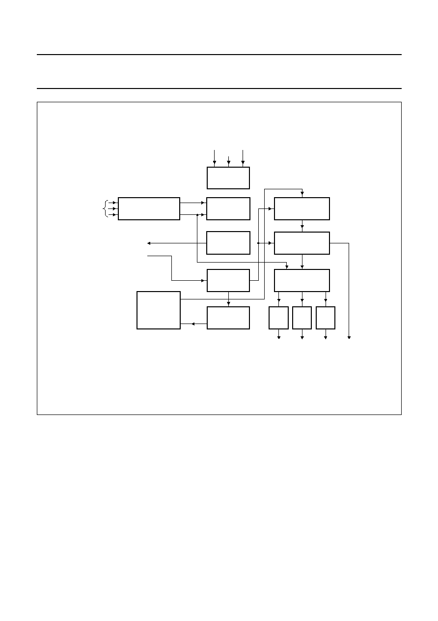
2000 Feb 23
57
Philips Semiconductors
Preliminary specification
Enhanced TV microcontrollers with
On-Screen Display (OSD)
SAA55xx
Fig.24 Display block diagram.
handbook, full pagewidth
MICROPROCESSOR
INTERFACE
DISPLAY
TIMING
HSYNC
CLK
VSYNC
CHARACTER
FONT
ADDRESSING
address
address
data
data
address
address
data
data
address
data
control
to memory interface
from memory interface
FUNCTION
REGISTERS
PARALLEL/SERIAL
CONVERTER
AND FRINGING
ATTRIBUTE
HANDLING
CLUT RAM
DISPLAY DATA
ADDRESSING
MBK965
CHARACTER
ROM
AND
DRCs
DATA
BUFFER
DAC
DAC
DAC
G
B
FB
R

2000 Feb 23
58
Philips Semiconductors
Preliminary specification
Enhanced TV microcontrollers with
On-Screen Display (OSD)
SAA55xx
19.2
Display modes
The display section has two distinct modes with different
features available in each. The two modes are:
∑
TXT: This is the display configured as the WST mode
with additional serial and global attributes. The display is
configured as a fixed 25 rows with 40 characters per
row.
∑
CC: This is the display configured as the US Closed
Caption mode. The display is configured as a maximum
of 16 rows with a maximum of 48 characters per row.
In both of the above modes the Character matrix, and
TV lines per row can be defined. There is an option of
9, 10, 13 and 16 TV lines per display row, and a Character
matrix (H
◊
V) of 12
◊
9, 12
◊
10, 12
◊
13, or 12
◊
16.
Not all combinations of TV lines per row and maximum
display rows give a sensible OSD display, since there is a
limited number of TV scan lines available.
Special Function Register TXT21 and memory mapped
registers are used to control the mode selection.
Throughout the section the features will be described and
their function in each of the modes given. If the feature is
different in either mode then this is stated.
19.2.1
F
EATURES AVAILABLE IN EACH MODE
Table 16 shows a list of features available in each mode,
and also if the setting is a serial/parallel attribute, or has a
global effect on all the display.
Table 16 Display features
FEATURE
TXT
CC
Flash
serial
serial
Boxes
Txt/OSD (serial)
serial
Horizontal size
x1, x2 or x4 (serial)
x1 or x2 (serial)
Vertical size
x1 or x2 (serial); x4 (global)
x1 or x2 (serial)
Italic
n/a
serial
Foreground colours
8 (serial)
8 + 8 (parallel)
Background colours
8 (serial)
16 (serial)
Soft colours (CLUT)
16 from 4096
16 from 4096
Underline
n/a
serial
Overline
n/a
serial
Fringe
N + S + E + W
N + S + E + W
Fringe colour
16 (global)
16 (serial)
Meshing of background
black or colour (global)
all (global)
Fast Blanking Polarity
yes
yes
Screen colour
16 (global)
16 (global)
DRCS
32 (global)
32 (global)
Character matrix (H
◊
V)
12
◊
9, 12
◊
10, 12
◊
13 or 12
◊
16
12
◊
9, 12
◊
10, 12
◊
13 or 12
◊
16
Number of rows
25
16
Number of columns
40
48
Number of characters displayable
1000
768
Cursor
yes
yes
Special graphics (2 planes per character)
16
16
Scroll
no
yes

2000 Feb 23
59
Philips Semiconductors
Preliminary specification
Enhanced TV microcontrollers with
On-Screen Display (OSD)
SAA55xx
19.3
Display feature descriptions
All display features are now described in detail for both
TXT and CC modes.
19.3.1
F
LASH
Flashing causes the foreground colour pixel to be
displayed as the background pixels. The flash frequency is
controlled by software setting and resetting the MMR
Status (see Table 34) at the appropriate interval.
CC: This attribute is valid from the time set (see Table 22)
until the end of the row or until otherwise modified.
TXT: This attribute is set by the control character `flash'
(08H) (see Fig.30) and remains valid until the end of the
row or until reset by the control character `steady' (09H).
19.3.2
B
OXES
CC: This attribute is valid from the time set until end of row
or otherwise modified if set with Serial Mode 0. If set with
Serial Mode 1, then it is set from the next character
onwards.
In text mode (within CC mode) the background colour is
displayed regardless of the setting of the box attribute bit.
Boxes take effect only during mixed mode, where boxes
are set in this mode the background colour is displayed.
Character locations where boxes are not set show
video/screen colour (depending on the setting in the MMR
Display Control) in stead of the background colour.
TXT: Two types of boxes exist the teletext box and the
OSD box. The teletext box is activated by the `start box'
control character (0BH). Two start box characters are
required to begin a teletext box, with the box starting
between the 2 characters. The box ends at the end of the
line or after a `end box' control character.
TXT mode can also use OSD boxes, they are started using
size implying OSD control characters
(BCH/BDH/BEH/BFH). The box starts after the control
character (set after) and ends either at the end of the row
or at the next size implying OSD character (set at).
The attributes flash, teletext box, conceal, separate
graphics, twist and hold graphics are all reset at the start
of an OSD box, as they are at the start of the row.
OSD boxes are only valid in TV mode which is defined by
TXT5 = 03H and TXT6 = 03H.
19.3.3
S
IZE
The size of the characters can be modified in both the
horizontal and vertical directions.
CC: Two sizes are available in both the horizontal and
vertical directions. The sizes available are normal (
◊
1),
double (
◊
2) height/width and any combination of these.
The attribute setting is always valid for the whole row.
Mixing of sizes within a row is not possible.
TXT: Three horizontal sizes are available normal (
◊
1),
double (
◊
2) and quadruple (
◊
4). The control characters
`normal size' (0CH/BCH) enables normal size, the `double
width' or double size (0EH/BEH/0FH/BFH) enables double
width characters.
Any two consecutive combination of `double width' or
`double size' (0EH/BEH/0FH/BFH) activates quadruple
width characters, provided quadruple width characters are
enabled by TXT4.QUAD WIDTH ENABLE.
Three vertical sizes are available normal(x1), double (x2)
and quadruple (x4). The control characters `normal size'
(0CH/BCH) enable normal size, the `double height' or
`double size' (0DH/BDH/0FH/BFH) enable double height
characters. Quadruple height character are achieved by
using double height characters and setting the global
attributes TXT7.DOUBLE HEIGHT (expand) and
TXT7.BOTTOM/TOP.
If double height characters are used in teletext mode,
single height characters in the lower row of the double
height character are automatically disabled.
19.3.4
I
TALIC
CC: This attribute is valid from the time set until the end of
the row or otherwise modified. The attribute causes the
character foreground pixels to be offset horizontally by
1 pixel per 4 scan lines (interlaced mode). The base is the
bottom left character matrix pixel. The pattern of the
character is indented as shown in Fig.25.
TXT: The Italic attribute is not available.
2000 Feb 23
60
Philips Semiconductors
Preliminary specification
Enhanced TV microcontrollers with
On-Screen Display (OSD)
SAA55xx
Fig.25 Italic characters.
handbook, full pagewidth
0
0
1
3
5
7
8
9
10
Field 1
12
◊
16 character matrix
12
◊
13 character matrix
indented by 7/6/4
indented by 6/5/3
indented by 5/4/2
indented by 4/3/1
indented by 3/2/0
indented by 2/1
indented by 1/0
MBK970
Field 2
11
12
13
14
15
2
2
4
4
6
6
8 10 0 2 4
6 8 10
indented by 0
0 2 4
6 8 10 0 2 4
6 8 10
12
◊
10 character matrix
0 2 4
6 8 10 0 2 4
6 8 10
19.3.5
C
OLOURS
A Colour Look-Up Table (CLUT) with 16 colour entries is
provided. The colours are programmable out of a palette
of 4096 (4 bits per R, G and B). The CLUT is defined by
writing data to a RAM that resides in the MOVX address
space of the 80C51.
Table 17 CLUT colour values
19.3.6
F
OREGROUND
C
OLOUR
CC: The foreground colour can be chosen from 8 colours
on a character by character basis. Two sets of 8 colours
are provided. A serial attribute switches between the
banks (see Table 22 Serial Mode 1, bit 7). The colours are
the CLUT entries 0 to 7 or 8 to 15.
TXT: The foreground colour is selected via a control
character (see Fig.29). The colour control characters takes
effect at the start of the next character (`Set-after') and
remain valid until the end of the row, or until modified by a
control character. Only 8 foreground colours are available.
The TEXT foreground control characters map to the CLUT
entries as shown in Table 18.
RED<3:0>
(B11 TO B8)
GREEN<3:0
> (B7 TO B4)
BLUE<3:0>
(B3 TO B0)
COLOUR
ENTRY
0000
0000
0000
0
0000
0000
1111
1
...
...
...
...
1111
1111
0000
14
1111
1111
1111
15
2000 Feb 23
61
Philips Semiconductors
Preliminary specification
Enhanced TV microcontrollers with
On-Screen Display (OSD)
SAA55xx
Table 18 Foreground CLUT mapping
19.3.7
B
ACKGROUND COLOUR
CC: This attribute is valid from the time set until end of row
or otherwise modified if set with Serial Mode 0. If set with
Serial Mode 1, then the colour is set from the next
character onwards.
The background colour can be chosen from all 16 CLUT
entries.
TXT: The control character `New background' (1DH) is
used to change the background colour to the current
foreground colour. The selection is immediate (set at) and
remains valid until the end of the row or until otherwise
modified.
The TEXT background control characters map to the
CLUT entries as shown in Table 19:
Table 19 Background CLUT mapping
19.3.8
B
ACKGROUND DURATION
The attribute when set takes effect from the current
position until the end of the text display defined in the MMR
Text Area End.
CC: The background duration attribute (see Table 22,
Serial Mode 1, bit 8) in combination with the End Of Row
attribute (see Table 22, Serial Mode 1, bit 9) forces the
background colour to be display on the row until the end of
the text area is reached.
TXT: This attribute is not available.
19.3.9
U
NDERLINE
The underline attribute causes the characters to have the
bottom scan line of the character cell forced to foreground
colour, including spaces. If background duration is set,
then underline is set until the end of the text area.
CC: The underline attribute (see Table 22, Serial
Mode 0/1, bit 4) is valid from the time set until end of row
or otherwise modified.
TXT: This attribute is not available.
19.3.10 O
VERLINE
The overline attribute causes the characters to have the
top scan line of the character cell forced to foreground
colour, including spaces. If background duration is set,
then overline is set until the end of the text area.
CC: The overline attribute (see Table 22, Serial Mode 0/1,
bit 5) is valid from the time set until end of row or otherwise
modified. Overlining of Italic characters is not possible.
TXT: This attribute is not available.
19.3.11 E
ND OF
R
OW
CC: The number of characters in a row is flexible and can
determined by the end of row attribute (see Table 22 Serial
Mode 1, bit 9). However the maximum number of
character positions displayed is determined by the setting
of the MMR Text Position Horizontal and MMR Text Area
End.
Note that when using the end of row attribute the next
character location after the attribute should always be
occupied by a `space'.
TXT: This attribute is not available, row length is fixed at
40 characters.
CONTROL
CODE
DEFINED
COLOUR
CLUT ENTRY
00H
black
0
01H
red
1
02H
green
2
03H
yellow
3
04H
blue
4
05H
magenta
5
06H
cyan
6
07H
white
7
CONTROL
CODE
DEFINED
COLOUR
CLUT ENTRY
00H + 1DH
black
8
01H + 1DH
red
9
02H + 1DH
green
10
03H + 1DH
yellow
11
04H + 1DH
blue
12
05H + 1DH
magenta
13
06H + 1DH
cyan
14
07H + 1DH
white
15
2000 Feb 23
62
Philips Semiconductors
Preliminary specification
Enhanced TV microcontrollers with
On-Screen Display (OSD)
SAA55xx
19.3.12 F
RINGING
A fringe (shadow) can be defined around characters.
The fringe direction is individually selectable in any of the
North, South, East and West direction using the MMR
Fringing Control. The colour of the fringe can also be
defined as one of the entries in the CLUT, again using
MMR Fringing Control.
CC: The fringe attribute (see Table 22, Serial Mode 0,
bit 9) is valid from the time set until the end of the row or
otherwise modified.
TXT: The display of fringing in TXT mode is controlled by
the TXT4.SHADOW ENABLE bit.
When set all the alphanumeric characters being displayed
are shadowed, graphics characters are not shadowed.
19.3.13 M
ESHING
The attribute effects the background colour being
displayed. Alternate pixels are displayed as the
background colour or video. The structure is offset by
1 pixel from scan line to scan line, thus achieving a
checker board display of the background colour and video.
CC: The setting of the MSH bit in MMR Display Control
has the effect of meshing any background colour.
TXT: There are two meshing attributes one that only
affects black background colours TXT4.B MESH ENABLE
and a second that only affects backgrounds other than
black TXT4.C MESH ENABLE. A black background is
defined as CLUT entry 8, a non-black background is
defined as CLUT entry 9 to 15.
Fig.26 South and south-west fringing.
handbook, full pagewidth
MBK972
handbook, full pagewidth
MBK973
Fig.27 Meshing and meshing/fringing (south + west).
2000 Feb 23
63
Philips Semiconductors
Preliminary specification
Enhanced TV microcontrollers with
On-Screen Display (OSD)
SAA55xx
19.3.14 C
URSOR
The cursor operates by reversing the background and
foreground colours in the character position pointed to by
the active cursor position. The cursor is enabled using
TXT7.CURSOR ON. When active, the row the cursor
appears on is defined by TXT9.R<4:0> and the column is
defined by TXT10.C<5:0>. The position of the cursor can
be fixed using TXT9.CURSOR FREEZE.
CC: The valid range for row is 0 to 15. The valid range for
column is 0 to 47. The cursor remains rectangular at all
times, it's shape is not affected by italic attribute, therefore
it is not advised to use the cursor with italic characters.
TXT: The valid range for row positioning is 0 to 24.
The valid range for column is 0 to 39.
19.3.15 S
PECIAL GRAPHICS CHARACTERS
CC/TXT: Several special characters are provided for
improved OSD effects. These characters provide a choice
of 4 colours within a character cell. The total number of
special graphics characters is limited to 16.
They are stored in the character codes 8XH and 9XH of
the character table (32 ROM characters), or in the DRCs
which overlay character codes 8XH and 9XH. Each
special graphics character uses two consecutive normal
characters.
Fringing, underline and overline is not possible for special
graphics characters. Special graphics characters are
activated when TXT20.OSD PLANES = 1.
If the screen colour is transparent (implicit in mixed mode)
and inside the object the box attribute is set, then the
object is surrounded by video. If the box attribute is not set
the background colour inside the object will also be
displayed as transparent.
Table 20 Special character colour allocation
PLANE 1
PLANE 0
COLOUR ALLOCATION
0
0
background colour
0
1
foreground colour
1
0
CLUT entry 6
1
1
CLUT entry 7
Fig.28 Cursor display.
handbook, full pagewidth
MBK971
A B
C
D E F
Fig.29 Special character example.
This example could also be done with 8 special characters.
handbook, full pagewidth
MGK550
VOLUME
background colour
"set at" (Mode 0)
background colour
"set after" (Mode 1)
serial attribute
foreground colour 7
background colour
special character
foreground colour
normal character
foreground colour 6

2000 Feb 23
64
Philips Semiconductors
Preliminary specification
Enhanced TV microcontrollers with
On-Screen Display (OSD)
SAA55xx
19.4
Character and attribute coding
This section describes the character and attribute coding
for each mode.
19.4.1
CC
MODE
Character coding is split into character oriented attributes
(parallel) and character group coding (serial). The serial
attributes take effect either at the position of the attribute
(set at), or at the following location (set after) and remain
effective until either modified by a new serial attribute or
until the end of the row. A serial attribute is represented as
a space (the space character itself however is not used for
this purpose), the attributes that are still active,
e.g. overline and underline will be visible during the display
of the space.
The default setting at the start of a row is:
∑
1
◊
size
∑
Flash off
∑
Overline off
∑
Underline off
∑
Italics off
∑
Display mode = superimpose
∑
Fringing off
∑
Background colour duration = 0
∑
End of row = 0.
The coding is done in 12-bit words. The codes are stored
sequentially in the display memory. A maximum of
768 character positions can be defined for a single display.
19.4.2
TXT
MODE
Character coding is in a serial format, with only one
attribute being changed at any single location. The serial
attributes take effect either at the position of the attribute
(set at), or at the following location (set after). The attribute
remains effective until either modified by new serial
attributes or until the end of the row.
The default settings at the start of a row are:
∑
Foreground colour white (CLUT address 7)
∑
Background colour black (CLUT address 8)
∑
Horizontal size
◊
1, vertical size
◊
1 (normal size)
∑
Alphanumeric on
∑
Contiguous Mosaic Graphics
∑
Release Mosaics
∑
Flash off
∑
Box off
∑
Conceal off
∑
Twist off.
The attributes have individual codes which are defined in
the basic character table (see Fig.30).
19.4.3
P
ARALLEL CHARACTER CODING
Table 21 Parallel character coding
BITS
DESCRIPTION
0 to 7
8-bit character code
8 to 10
3 bits for 8 foreground colours
11
Mode bit: 0 = parallel code

2000 Feb 23
65
Philips Semiconductors
Preliminary specification
Enhanced TV microcontrollers with
On-Screen Display (OSD)
SAA55xx
19.4.4
S
ERIAL CHARACTER CODING
Table 22 Serial character coding
BITS
DESCRIPTION
SERIAL MODE 0
(`SET AT')
SERIAL MODE 1
CHAR.POS. 1 (`SET AT')
CHAR.POS. >1 (`SET AFTER')
0 to 3 4 bits for 16 background colours
4 bits for 16 background colours
4 bits for 16 background colours
4
Underline switch:
Horizontal size:
Underline switch:
0 = underline off
0 = normal
0 = underline off
1 = underline on
1 =
◊
2
1 = underline on
5
Overline switch:
Vertical size:
Overline switch:
0 = overline off
0 = normal
0 = overline off
1 = overline on
1 =
◊
2
1 = overline on
6
Display mode:
Display mode:
Display mode:
0 = superimpose
0 = superimpose
0 = superimpose
1 = boxing
1 = boxing
1 = boxing
7
Flash switch:
Foreground colour switch
Foreground colour switch
0 = flash off
0 = Bank 0 (colours 0 to 7)
0 = Bank 0 (colours 0 to 7)
1 = flash on
1 = Bank 1 (colours 8 to 15)
1 = Bank 1 (colours 8 to 15)
8
Italic switch:
Background colour duration:
Background colour duration (set
at):
0 = italics off
0 = stop BGC
0 = stop BGC
1 = italics on
1 = set BGC to end of row
1 = set BGC to end of row
9
Fringing switch:
End of row
End of row (set at):
0 = fringing off
0 = continue row
0 = continue row
1 = fringing on
1 = end row
1 = end row
10
Switch for serial coding:
Switch for serial coding:
Switch for serial coding:
0 = mode 0
1 = mode 1
0 = mode 0
1 = mode 1
0 = mode 0
1 = mode 1
11
Mode bit:
Mode bit:
Mode bit:
1 = serial code
1 = serial code
1 = serial code
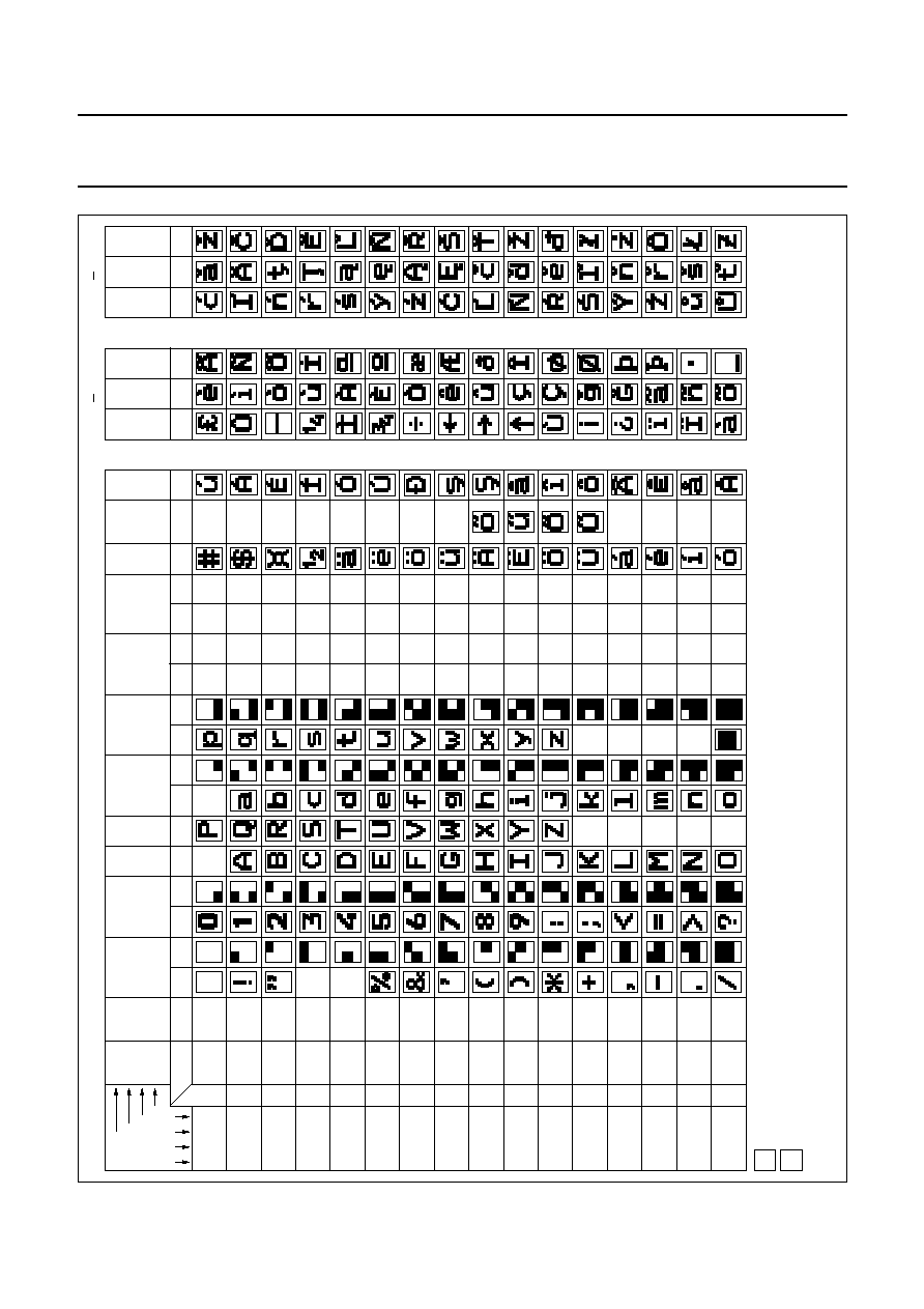
2000
Feb
23
66
Philips Semiconductors
Preliminar
y specification
Enhanced TV microcontrollers with
On-Screen Displa
y (OSD)
SAA55xx
This text is here in white to force landscape pages to be rotated correctly when browsing through the pdf in the Acrobat reader.This text is here in
_
white to force landscape pages to be rotated correctly when browsing through the pdf in the Acrobat reader.This text is here inThis text is here in
white to force landscape pages to be rotated correctly when browsing through the pdf in the Acrobat reader. white to force landscape pages to be ...
handbook, full pagewidth
MBK974
normal
height
b3 b2 b1 b0
b4
b5
b6
b7
0
1
2
2a
3
3a
4
5
6
6a
7
7a
8
8a
9a
9
C
column
r
o
w
B
I
T
S
0
0
0
0
0
0
0
1
0
1
0
0
0
1
0
1
1
0
0
0
1
0
0
1
A
1
0
1
0
1
1
0
0
0
1
1
0
0
0
1
1
0
0
1
0
0
1
1
1
E
1 1 1 0
double
width
hold
graphics
F
1 1 1 1
double
size
release
graphics
B
1 0 1 1
start box
twist
C
1 1 0 0
black
back -
ground
D
1 1 0 1
double
height
new
back -
ground
A
1 0 1 0
end box
separated
graphics
9
1 0 0 1
steady
contiguous
graphics
8
1 0 0 0
flash
conceal
display
7
0 1 1 1
alpha
white
graphics
white
6
0 1 1 0
alpha
cyan
graphics
cyan
5
0 1 0 1
alpha
magenta
graphics
magenta
4
0 1 0 0
alpha
blue
graphics
blue
3
0 0 1 1
alpha
yellow
graphics
yellow
2
0 0 1 0
alpha
green
graphics
green
0
0 0 0 0
alpha
black
graphics
black
1
0 0 0 1
alpha
red
graphics
red
B
1
0
1
1
D
E
F
1
1
0
1
1
1
1
0
1
1
1
1
D
E
F
1
1
0
1
1
1
1
0
1
1
1
1
double
width
OSD
double
size
OSD
OSD
OSD
OSD
OSD
OSD
OSD
OSD
OSD
OSD
OSD
OSD
OSD
OSD
OSD
OSD
OSD
OSD
OSD
OSD
OSD
OSD
OSD
OSD
OSD
OSD
OSD
OSD
OSD
OSD
OSD
OSD
E/W = 0
E/W = 1
OSD
OSD
OSD
OSD
OSD
OSD
OSD
OSD
OSD
OSD
OSD
OSD
OSD
OSD
OSD
OSD
OSD
OSD
OSD
OSD
OSD
OSD
OSD
OSD
OSD
OSD
OSD
OSD
OSD
OSD
OSD
OSD
OSD
nat
opt
nat
opt
nat
opt
nat
opt
nat
opt
nat
opt
nat
opt
nat
opt
nat
opt
nat
opt
nat
opt
nat
opt
nat
opt
nat
opt
normal
size
OSD
double
height
OSD
back-
ground
white
back-
ground
cyan
back-
ground
magenta
back-
ground
blue
back-
ground
yellow
back-
ground
green
back-
ground
black
back
ground
red
OSD
character dependent on the language of page, refer to National Option characters
customer definable On-Screen Display character
Fig.30 TXT basic character set (Pan-European).

2000 Feb 23
67
Philips Semiconductors
Preliminary specification
Enhanced TV microcontrollers with
On-Screen Display (OSD)
SAA55xx
19.5
Screen and global controls
A number of attributes are available that affect the whole
display region, and cannot be applied selectively to
regions of the display.
19.5.1
TV
SCAN LINES PER ROW
The number of TV scan lines per field used for each
display row can be defined, the value is independent of the
character size being used. The number of lines can be
either 10, 13 or 16 per display row. The number of TV scan
lines per row is defined TXT21.DISP LINES<1:0>.
A value of 9 lines per row can be achieved if the display is
forced into 525-line display mode by
TXT17.FORCE DISP<1:0>, or if the device is in 10 line
mode and the automatic detection circuitry within display
finds 525-line display syncs.
19.5.2
C
HARACTER MATRIX
(H
◊
V)
There are three different character matrices available,
these are 12
◊
10, 12
◊
13 and 12
◊
16. The selection is
made using TXT21.CHAR SIZE<1:0> and is independent
of the number of display lines per row.
If the character matrix is less than the number of TV scan
lines per row then the matrix is padded with blank lines.
If the character matrix is greater than the number of
TV scan lines then the character is truncated.
19.5.3
D
ISPLAY MODES
CC: When attributes superimpose or boxing (see
Table 22, Serial Mode 0/1, bit 6) are set, the resulting
display depends on the setting of the following screen
control mode bits in the MMR Display Control.
TXT: The display mode is controlled by the bits in the
TXT5 and TXT6. There are 3 control functions - Text on,
Background on and Picture on. Separate sets of bits are
used inside and outside teletext boxes so that different
display modes can be invoked. TXT6 is used if the
newsflash (C5) or subtitle (C6) bits in row 25 of the basic
page memory are set otherwise TXT5 is used. This allows
the software to set up the type of display required on
newsflash and subtitle pages (e.g. text inside boxes,
TV picture outside) this will be invoked without any further
software intervention when such a page is acquired.
When teletext box control characters are present in the
display page memory, the appropriate Box control bit must
be set, TXT7.BOX ON 0, TXT7.BOX ON 1
-
23 or
TXT7.BOX ON 24. This allows the display mode to be
different inside the teletext box compared to outside.
These bits are present to allow boxes in certain areas of
the screen to be disabled. The use of teletext boxes for
OSD messages has been superseded in this device by the
OSD box concept, but these bits remain to allow teletext
boxes to be used, if required.
Table 23 Selection of Display modes
Table 24 TXT display control bits
MOD1
MOD0
DISPLAY MODE
DESCRIPTION
0
0
Video
Disables all display activities, sets the RGB to true black and VDS to video.
0
1
Full Text
Displays screen colour at all locations not covered by character foreground
or background colour. The box attribute has no effect.
1
0
Mixed Screen Colour
Displays screen colour at all locations not covered by character foreground,
within boxed areas or, background colour.
1
1
Mixed Video
Displays video at all locations not covered by character foreground, within
boxed areas or, background colour.
PICTURE ON
TEXT ON
BACKGROUND ON
EFFECT
0
0
X
Text mode, black screen
0
1
0
Text mode, background always black
0
1
1
Text mode
1
0
X
Video mode
1
1
0
Mixed text and TV mode
1
1
1
Text mode, TV picture outside text area

2000 Feb 23
68
Philips Semiconductors
Preliminary specification
Enhanced TV microcontrollers with
On-Screen Display (OSD)
SAA55xx
19.6
Screen colour
Screen colour is displayed from 10.5 to 62.5 ms after the
active edge of the HSYNC input and on TV lines 23 to 310
inclusive, for a 625-line display, and lines 17 to 260
inclusive for a 525-line display.
CC: The screen colour is defined by the MMR Display
Control and points to a location in the CLUT table.
The screen colour covers the full video width. It is visible
when the Full Text or Mixed Screen Colour mode is set
and no foreground or background pixels are being
displayed.
TXT: The register bits TXT17.SCREEN COL<2:0> can be
used to define a colour to be displayed in place of
TV picture and the black background colour. If the bits are
all set to zero, the screen colour is defined as `transparent'
and TV picture and background colour are displayed as
normal. Otherwise the bits define CLUT entries 9 to 15.
19.7
Text display controls
19.7.1
T
EXT DISPLAY CONFIGURATION
(CC
MODE
)
Two types of areas are possible. The one area is static and
the other is dynamic. The dynamic area allows scrolling of
a region to take place. The areas cannot cross each other.
Only one scroll region is possible.
19.7.2
D
ISPLAY MAP
The display map allows a flexible allocation of data in the
memory to individual rows.
Sixteen words are provided in the display memory for this
purpose. The lower 10 bits address the first word in the
memory where the row data starts. This value is an offset
in terms of 16-bit words from the start of Display memory
(8000H). The most significant bit enables the display when
not within the scroll (dynamic) area.
The display map memory is fixed at the first 16 words in
the closed caption display memory.
Table 25 Display map bit allocation
BIT
FUNCTION
11
Text display enable, valid outside Soft Scroll
Area. 0 = disable; 1 = enable.
10
This bit is reserved, should be set to logic 0.
9 to 0
Pointer to row data.

2000 Feb 23
69
Philips Semiconductors
Preliminary specification
Enhanced TV microcontrollers with
On-Screen Display (OSD)
SAA55xx
Fig.31 Display map and data pointers.
handbook, full pagewidth
MBK966
0
1
2
3
4
5
6
7
8
9
10
11
12
13
14
15
0
1
2
3
4
10
11
3
4
9
10
11
12
13
14
15
display
possible
soft scrolling
display possible
display
possible
display
map
entries
display
data
Display memory
Text area
ROW
Enable
bit = 0

2000 Feb 23
70
Philips Semiconductors
Preliminary specification
Enhanced TV microcontrollers with
On-Screen Display (OSD)
SAA55xx
19.8
Soft scroll action
The dynamic scroll region is defined by the MMR Scroll
Area, MMR Scroll Range, MMR Top Scroll line and the
MMR Status. The scroll area is enabled when the SCON
bit is set in MMR Status.
The position of the soft scroll area window is defined using
the Soft Scroll Position bits (SSP<3:0>) and the height of
the window is defined using the Soft Scroll Height bits
(SSH<3:0>) both are in MMR Scroll Range. The rows that
are scrolled through the window are defined using the Start
Scroll Row (STS<3:0>) and the Stop Scroll Row
(SPS<3:0>) both are in MMR Scroll Area.
The soft scrolling function is done by modifying the Scroll
Line (SCL<3:0>) in MMR Top Scroll Line and the first scroll
row value SCR<3:0> in the MMR Status.
If the number of rows allocated to the scroll counter is
larger than the defined visible scroll area, this allows parts
of rows at the top and bottom to be displayed during the
scroll function. The registers can be written throughout the
field and the values are updated for display with the next
field sync. Care should be taken that the register pairs are
written to by the software in the same field.
Only a region that contains only single height rows or only
double height rows can be scrolled.
TXT: The display is organised as a fixed size of 25 rows
(0 to 24) of 40 columns (0 to 39). This is the standard size
for teletext transmissions. The control data in row 25 is not
displayed but is used to configure the display page
correctly.
Fig.32 Soft scroll area.
handbook, full pagewidth
15
MBK967
14
13
12
11
10
9
8
7
6
5
soft scroll position
pointer SSP<3:0> e.g. 6
soft scroll height
SSH<3:0> e.g. 4
soft scrolling area
usable for
OSD display
usable for
OSD display
should not be used
for OSD display
should not be used
for OSD display
start scroll row
STS<3:0> e.g. 3
start scroll row
SPS<3:0> e.g. 11
4
3
2
1
0
ROW
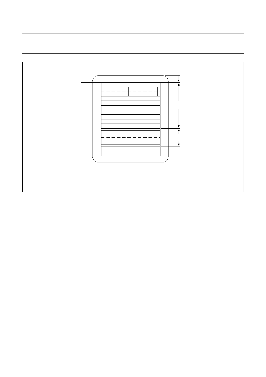
2000 Feb 23
71
Philips Semiconductors
Preliminary specification
Enhanced TV microcontrollers with
On-Screen Display (OSD)
SAA55xx
Fig.33 CC text areas.
handbook, full pagewidth
MBK977
ROW
0
row0
row1
1
2
3
4
5
6
7
8
9
10
11
12
13
14
15
row2
row3
row4
row5
row6
row7
Closed Captioning data row n
Closed Captioning data row n
+
1
Closed Captioning data row n
+
2
Closed Captioning data row n
+
3
Closed Captioning data row n
+
4
row8
row13
visible area
for scrolling
scroll area
offset
0-63
lines
row14
P01 NBC
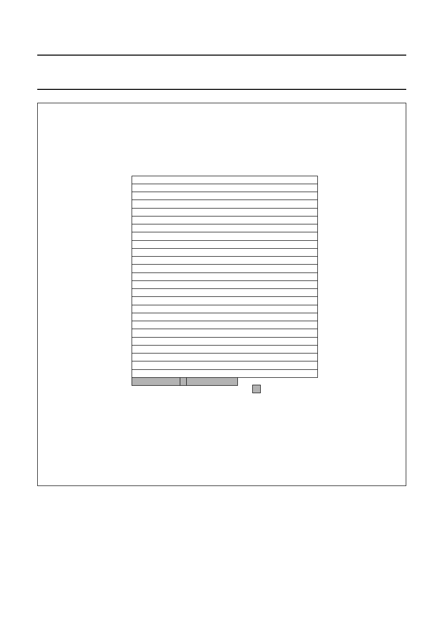
2000 Feb 23
72
Philips Semiconductors
Preliminary specification
Enhanced TV microcontrollers with
On-Screen Display (OSD)
SAA55xx
Fig.34 TXT text area.
handbook, full pagewidth
0
9
0
23
39
10
MBK968
control data
non-displayable data
byte 10 reserved
Row 0
1
2
3
4
5
6
7
8
9
10
11
12
13
14
15
16
17
18
19
20
21
22
23
24
25

2000 Feb 23
73
Philips Semiconductors
Preliminary specification
Enhanced TV microcontrollers with
On-Screen Display (OSD)
SAA55xx
19.9
Display positioning
The display consists of the screen colour covering the whole screen and the text area that is placed within the visible
screen area.
The screen colour extends over a large vertical and horizontal range so that no offset is needed. The text area is offset
in both directions relative to the vertical and horizontal sync pulses.
Fig.35 Display area positioning.
handbook, full pagewidth
MGL150
56
µ
s
text area start
0.25 character
offset
horizontal
sync
delay
horizontal sync
vertical
sync
6 lines
offset
text
vertical
offset
screen colour
offset = 8
µ
s
text area end
SCREEN COLOUR AREA
TEXT AREA

2000 Feb 23
74
Philips Semiconductors
Preliminary specification
Enhanced TV microcontrollers with
On-Screen Display (OSD)
SAA55xx
19.9.1
S
CREEN COLOUR DISPLAY AREA
This area is covered by the screen colour. The screen
colour display area starts with a fixed offset of 8
µ
s from
the leading edge of the horizontal sync pulse in the
horizontal direction. A vertical offset is not necessary.
Table 26 Screen colour display area
19.9.2
T
EXT DISPLAY AREA
The text area can be defined to start with an offset in both
the horizontal and vertical direction.
Table 27 Text display area
The horizontal offset is set in the MMR Text Area Start.
The offset is done in full width characters using TAS<5:0>
and quarter characters using HOP<1:0> for fine setting.
The values 00H to 08H for TAS<5:0> will result in a
corrupted display.
The value 09H should also be avoided in the MMR Text
Area Start as corruption of the row 24 display can occur.
Alternative values are C8H or 49H to overcome this
problem.
The width of the text area is defined in the Text Area End
Register by setting the end character value TAE<5:0>.
This number determines where the background colour of
the Text Area will end if set to extend to the end of the row.
It will also terminate the character fetch process thus
eliminating the necessity of a row end attribute. This
entails however writing to all positions.
The vertical offset is set in the Text Position Vertical
Register. The offset value VOL<5:0> is done in number of
TV scan lines.
Note that the Text Position Vertical register should not be
set to 00H as the Display Busy interrupt is not generated
in these circumstances.
19.10 Character set
To facilitate the global nature of the device the character
set has the ability to accommodate a large number of
characters, which can be stored in different matrices.
POSITION
525-LINE
Horizontal
Start at 8
µ
s after leading edge of
horizontal sync for 56
µ
s.
Vertical
Line 9, Field 1 (321, Field 2) to leading
edge of vertical sync (line numbering
using 625 standard).
POSITION
DESCRIPTION
Horizontal
Up to 48 full sized characters per row.
Start position setting from 8 to 64
characters from the leading edge of
horizontal sync. Fine adjustment in
quarter characters.
Vertical
256 lines (nominal 41 to 297). Start
position setting from leading edge of
vertical sync, legal values are
4 to 64 lines (line numbering using
625 standard).
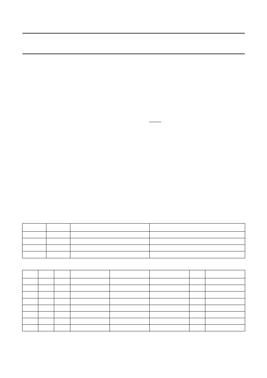
2000 Feb 23
75
Philips Semiconductors
Preliminary specification
Enhanced TV microcontrollers with
On-Screen Display (OSD)
SAA55xx
19.10.1 C
HARACTER MATRICES
The character matrices that can be accommodated in both
display modes are:
(H
◊
V
◊
planes) 12
◊
9
◊
1, 12
◊
10
◊
1, 12
◊
13
◊
1,
12
◊
16
◊
1.
These modes allow two colours per character position.
In CC mode two additional character matrices are
available to allow four colours per character.
(H
◊
V
◊
planes) 12
◊
13
◊
2, 12
◊
16
◊
2.
The characters are stored physically in ROM in a matrix of
size either 12
◊
10 or 12
◊
16.
19.10.2 C
HARACTER SET SELECTION
Four character sets are available in the device. A set can
consist of alphanumeric characters as required by the
WST or US Closed Captioning, Customer definable
On-Screen Display characters, and Special Graphic
characters.
CC: Only a single character set can be used for display
and this is selected using the Basic Set selection
TXT18.BS<1:0>. When selecting a character set in
CC mode the Twist Set selection TXT19.TS<1:0> should
be set to the same value as TXT18.BS<1:0> for correct
operation.
TXT: Two character sets can be displayed at once. These
are the basic G0 set or the alternative G0 set (Twist Set).
The basic set is selected using TXT18.BS<1:0>.
The alternative/twist character set is defined by
TXT19.TS<1:0>. Since the alternative character set is an
option it can be enabled or disabled using TXT19.TEN,
and the language code that is defined for the alternative
set is defined by TXT19.TC<2:0>.
The National option table is selected using
TXT18.NOT<3:0>. A maximum of 31 National option
tables can be defined when combined with the
EAST/WEST control bit located in register TXT4.
An example of the character set selection and definitions
is show in Table 28.
An example of the National option reference table is shown
in Table 29. Only a certain number of national options will
be relevant for each of the Character sets.
Table 28 Character set selection
Table 29 National option selection
BS1/TS1
BS0/TS0
CHARACTER SET
EXAMPLE LANGUAGE
0
0
Set 0
Latin
0
1
Set 1
Greek
1
0
Set 2
Cyrillic
1
1
Set 3
French/Arabic
C12
C13
C14
NOT<3:0> = 0000
NOT<3:0> = 0001
NOT<3:0> = 0010
...
NOT<3:0> = 1110
0
0
0
English
Polish
English
...
Polish
0
0
1
German
German
German
...
German
0
1
0
Swedish
Swedish
Swedish
...
Estonian
0
1
1
Italian
Italian
Italian
...
Lettish
1
0
0
French
French
French
...
Russian
1
0
1
Spanish
-
Spanish
...
Serb-Croat
1
1
0
Czech
Czech
Turkish
...
Czech
1
1
1
-
-
-
...
-

2000 Feb 23
76
Philips Semiconductors
Preliminary specification
Enhanced TV microcontrollers with
On-Screen Display (OSD)
SAA55xx
19.11 ROM addressing
Three ROMs are used to generate the correct pixel information. The first contains the National option look-up table, the
second contains the Basic Character look-up table and the third contains the Character Pixel information.
Although these are individual ROMs, since they do not need to be accessed simultaneously they are all combined into
a single ROM unit.
Fig.36 ROM organisation.
handbook, full pagewidth
MBK978
LOOK-UP SET 3
0800H
0600H
0400H
0200H
0000H
0800H
2400H
0000H
LOOK-UP SET 2
CHARACTER PIXEL DATA
(71680
◊
12-BIT)
LOOK-UP
BASIC + NATIONAL OPTION
2048 LOCATIONS
710 TEXT
OR
430 TEXT
+
176 CC
LOOK-UP SET 1
LOOK-UP SET 0
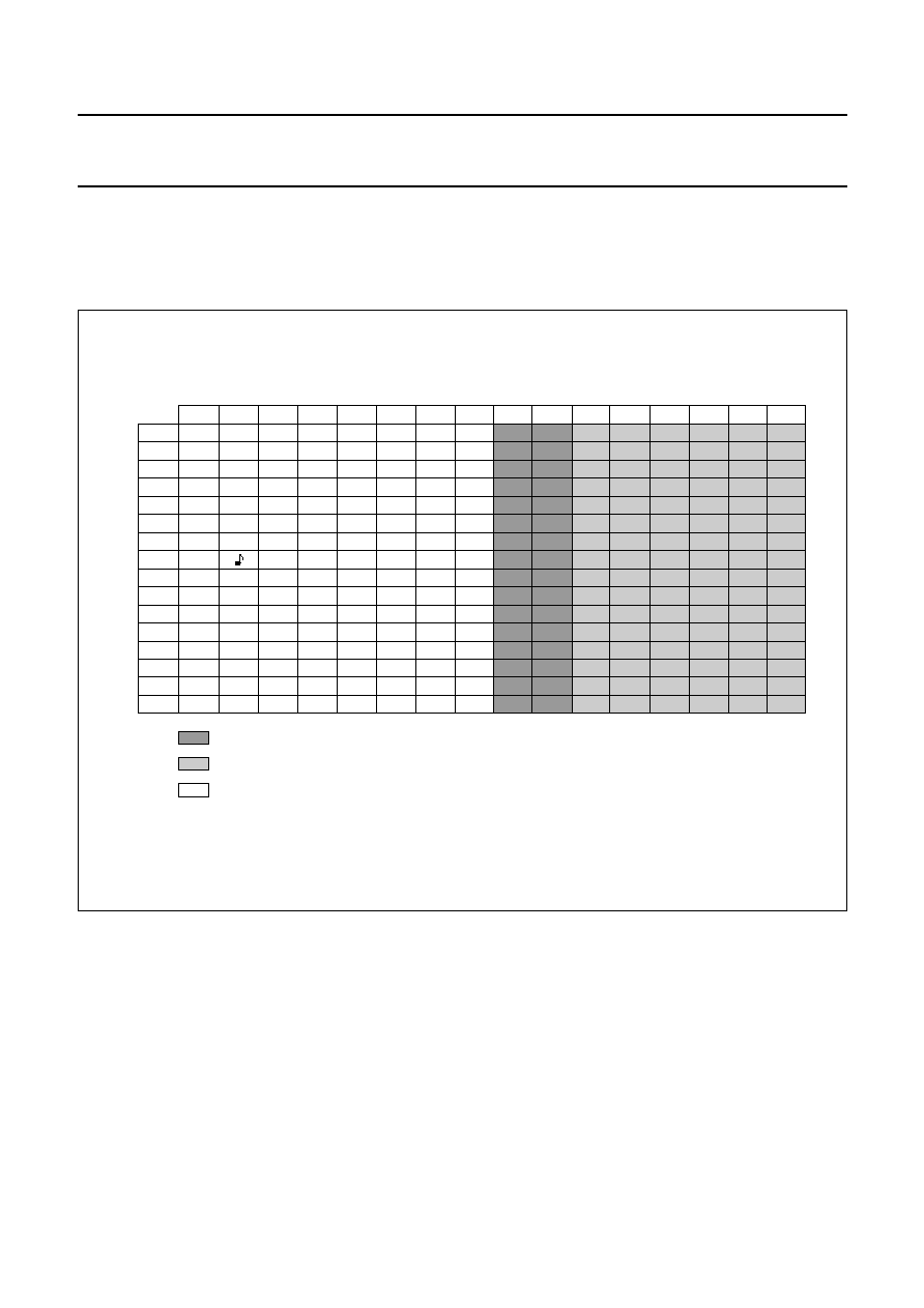
2000 Feb 23
77
Philips Semiconductors
Preliminary specification
Enhanced TV microcontrollers with
On-Screen Display (OSD)
SAA55xx
19.11.1 C
HARACTER TABLE
CC: The character table is shown in Fig.37.
TXT: One of the character set options (Pan-European: Latin) is shown in Fig.30.
Fig.37 Closed Caption character table.
handbook, full pagewidth
MBK976
0
0
1
2
3
4
5
6
7
A
B
C
D
E
F
8
9
Æ
SP
0
@
P
˙
p
∞
!
1
A
Q
a
q
1/2
"
2
B
R
b
r
ø
#
3
C
S
c
s
TM
$
4
D
T
d
t
¢
%
5
E
U
e
u
1
2
3
4
5
6
7
8
9
A
B
C
D
E
F
£
&
6
F
V
f
v
¥
7
G
W
g
w
ý
(
8
H
X
h
x
_
)
9
I
Y
i
y
Ë
·
:
J
Z
j
z
‚
+
;
K
[
k
Á
Í
,
<
L
È
l
Ó
-
=
M
]
m
—
Ù
.
>
N
Õ
n
Ò
˚
/
?
O
Û
o
n
Character code columns (bits 4 to 7)
Special characters in column 8 and 9
Additional table locations for normal characters
Table locations for normal characters
Character code rows (bits 0 to 3)
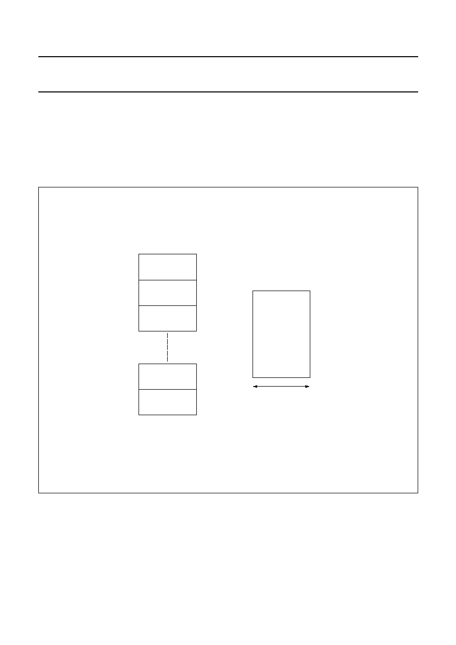
2000 Feb 23
78
Philips Semiconductors
Preliminary specification
Enhanced TV microcontrollers with
On-Screen Display (OSD)
SAA55xx
19.12 Redefinable characters
A number of Dynamically Redefinable Characters (DRC)
are available. These are mapped onto the normal
character codes, and replace the predefined ROM value.
There are 32 DRCs, the first 16 occupy the character
codes 80H to 8FH, the second 16 occupy the locations
90H to 9FH. This allows for 32 DRCs or 16 Special DRCs.
The remapping of the standard OSD to the DRCs is
activated when the TXT20.DRCS ENABLE bit is set.
The selection of Normal or Special OSD symbols is
defined by the TXT20.OSD PLANES.
Each character is stored in a matrix of 12
◊
16
◊
1
(V
◊
H
◊
planes), this allows for all possible character
matrices to be defined within a single location.
Fig.38 Organisation of DRC RAM.
handbook, full pagewidth
MBK969
CHARACTER 0
address (HEX)
character code
character 0
address (HEX)
80H
00
01
02
03
04
05
06
07
08
09
0A
0B
0C
0D
0E
0F
CHARACTER 1
81H
CHARACTER 2
82H
8800
881F
8820
883F
8840
885F
CHARACTER 30
9EH
CHARACTER 31
12 bits
9FH
8BC0
8BDF
8BE0
8BFF
A
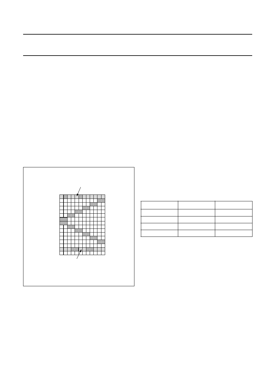
2000 Feb 23
79
Philips Semiconductors
Preliminary specification
Enhanced TV microcontrollers with
On-Screen Display (OSD)
SAA55xx
19.12.1 D
EFINING CHARACTERS
The DRC RAM is mapped into the 80C51 RAM address
space and starts at location 8800H. The character matrix
is 12 bits wide and therefore requires two bytes to be
written for each word, the first byte (even addresses),
addresses the lower 8 bits and the lower nibble of the
second byte (odd addresses) addresses the upper 4 bits.
For characters of 9, 10 or 16 lines high the pixel
information starts in the first address and continues
sequentially for the required number of address.
Characters of 13 lines high are defined with an initial offset
of 1 address, this is to allow for correct generation of
fringing across boundaries of clustered characters see
Fig.39. The characters continue sequentially for 13 lines
after which a further line can again be used for generation
of correct fringing across boundaries of clustered
characters.
19.13 Display synchronization
The horizontal and vertical synchronizing signals from the
TV deflection are used as inputs. Both signals can be
inverted before being delivered to the Phase Selector
section.
CC: The polarity is controlled using either VPOL or HPOL
bits in the MMR Text Position Vertical.
TXT: The TXT1.H POLARIY and TXT1.V POLARITY bits
control the polarity.
A line locked 12 MHz clock is derived from the 12 MHz free
running oscillator by the Phase Selector. This line locked
clock is used to clock the whole of the display block.
The horizontal and vertical sync signals are synchronized
with the 12 MHz clock before being used in the display
section.
19.14 Video/data switch (Fast Blanking) polarity
The polarity of the Video/data (Fast Blanking) signal can
be inverted. The polarity is set with the VDSPOL bit in the
MMR RGB Brightness.
Table 30 Fast Blanking signal polarity
19.15 Video/Data switch adjustment
To take into account the delay between the RGB values
and the VDS signal due to external buffering, the VDS
signal can be moved in relation to the RGB signals.
The VDS signal can be set to be either a clock cycle before
or after the RGB signal, or coincident with the RGB signal.
This is done using VDEL<2:0> in the MMR Configuration.
Fig.39 13 line high DRCs character format.
handbook, halfpage
line 13 from
character above
line 1 from
character below
top left
pixel
MSB
LSB
MBK975
HEX
440
003
00C
030
0C0
300
C00
C00
300
0C0
030
00C
003
000
1A8
000
line
number
0
1
2
3
4
5
6
7
8
9
10
11
12
13
14
15
fringing
top line
bottom right
pixel
bottom line
fringing
line not used
VDSPOL
VDS
CONDITION
0
1
RGB display
0
0
Video display
1
0
RGB display
1
1
Video display

2000 Feb 23
80
Philips Semiconductors
Preliminary specification
Enhanced TV microcontrollers with
On-Screen Display (OSD)
SAA55xx
19.16 RGB brightness control
A brightness control is provided to allow the RGB upper
output voltage level to be modified. The nominal value is
1 V into a 150
resistor, but can be varied between
0.7 and 1.2 V.
The brightness is set in RGB Brightness Register.
Table 31 RGB brightness
19.17 Contrast reduction
CC: This feature is not available in CC mode.
TXT: The COR bits in SFRs TXT5 and TXT6 control when
the COR output of the device is activated (i.e. pulled
LOW). This output is intended to act on the TVs display
circuits to reduce contrast of the video when it is active.
The result of contrast reduction is to improve the
readability of the text in a mixed teletext and video display.
The bits in the TXT5 and TXT6 SFRs allow the display to
be set up so that, for example, the areas inside teletext
boxes will be contrast reduced when a subtitle is being
displayed but that the rest of the screen will be displayed
as normal video.
20 MEMORY MAPPED REGISTERS (MMR)
The memory mapped registers are used to control the
display. The registers are mapped into the microcontroller
MOVX address space, starting at address 87F0H and
extending to 87FFH.
Table 32 MMR address summary
BRI3 TO BRI0
RGB BRIGHTNESS
0000
lowest value
...
...
1111
highest value
REGISTER
NUMBER
MEMORY
ADDRESS
FUNCTION
0
87F0H
Display Control
1
87F1H
Text Position Vertical
2
87F2H
Text Area Start
3
87F3H
Fringing Control
4
87F4H
Text Area End
5
87F5H
Scroll Area
6
87F6H
Scroll Range
7
87F7H
RGB Brightness
8
87F8H
Status
9
87F9H
Reserved
10
87FAH
Reserved
11
87FBH
Reserved
12
87FCH
HSYNC Delay
13
87FDH
VSYNC Delay
14
87FEH
Top Scroll Line
15
87FFH
Configuration

2000 Feb 23
81
Philips Semiconductors
Preliminary specification
Enhanced TV microcontrollers with
On-Screen Display (OSD)
SAA55xx
Table 33 MMR map
ADD
R/W
NAME
7
6
5
4
3
2
1
0
RESET
87F0
R/W Display
Control
SRC3
SRC2
SRC1
SRC0
-
MSH
MOD1
MOD0
00H
87F1
R/W Text Position
Vertical
VPOL
HPOL
VOL5
VOL4
VOL3
VOL2
VOL1
VOL0
00H
87F2
R/W Text Area
Start
HOP1
HOP0
TAS5
TAS4
TAS3
TAS2
TAS1
TAS0
00H
87F3
R/W Fringing
Control
FRC3
FRC2
FRC1
FRC0
FRDN
FRDE
FRDS
FRDW
00H
87F4
R/W Text Area
End
-
-
TAE5
TAE4
TAE3
TAE2
TAE1
TAE0
00H
87F5
R/W Scroll Area
SSH3
SSH2
SSH1
SSH0
SSP3
SSP2
SSP1
SSP0
00H
87F6
R/W Scroll Range
SPS3
SPS2
SPS1
SPS0
STS3
STS2
STS1
STS0
00H
87F7
R/W RGB
Brightness
VDSPOL
-
-
-
BRI3
BRI2
BRI1
BRI0
00H
87F8
R
Status
BUSY
FIELD
SCON
FLR
SCR3
SCR2
SCR1
SCR0
00H
W
-
-
SCON
FLR
SCR3
SCR2
SCR1
SCR0
00H
87FC R/W HSYNC
Delay
-
HSD6
HSD5
HSD4
HSD3
HSD3
HSD1
HSD0
00H
87FD R/W VSYNC
Delay
-
VSD6
VSD5
VSD4
VSD3
VSD2
VSD1
VSD0
00H
87FE R/W Top Scroll
Line
-
-
-
-
SCL3
SCL2
SCL1
SCL0
00H
87FF
R/W Configuration CC
VDEL2
VDEL1
VDEL0
TXT/V
-
-
-
00H

2000 Feb 23
82
Philips Semiconductors
Preliminary specification
Enhanced TV microcontrollers with
On-Screen Display (OSD)
SAA55xx
Table 34 MMR bit definition
REGISTER
FUNCTION
Display Control
SRC3 to SRC0
screen colour definition
MSH
meshing all background colours (logic 1)
MOD2 to MOD0
00 = Video
01 = Full Text
10 = Mixed Screen Colour
11 = Mixed Video
Text Position Vertical
VPOL
inverted input polarity (logic 1)
HPOL
inverted input polarity (logic 1)
VOL5 to VOL0
display start vertical offset from VSYNC (lines)
Text Area Start
HOP1 to HOP0
fine horizontal offset in quarter of characters
TAS5 to TAS0
text area start
Fringing Control
FRC3 to FRC0
fringing colour, value address of CLUT
FRDN
fringe in north direction (logic 1)
FRDE
fringe in east direction (logic 1)
FRDS
fringe in south direction (logic 1)
FRDW
fringe in west direction (logic 1)
Text Area End
TAE5 to TAE0
text area end, in full characters
Scroll Area
SSH3 to SSH0
soft scroll height
SSP3 to SSP0
soft scroll position
Scroll Range
SPS3 to SPS0
stop scroll row
STS3 to STS0
start scroll row
RGB Brightness
VDSPOL
VDS polarity
0 = RGB (1), Video (0)
1 = RGB (0), Video (1)
BRI3 to BRI0
RGB brightness control

2000 Feb 23
83
Philips Semiconductors
Preliminary specification
Enhanced TV microcontrollers with
On-Screen Display (OSD)
SAA55xx
Status read
BUSY
access to display memory could cause display problems (logic 1)
FIELD
even field (logic 1)
FLR
active flash region background only displayed (logic 1)
SCR3 to SCR0
first scroll row
Status write
SCON
scroll area enabled (logic 1)
FLR
active flash region background colour only displayed (logic 1)
SCR3 to SCR0
first scroll row
HSYNC Delay
HSD6 to HSD0
HSYNC delay, in full size characters
VSYNC Delay
VSD6 to VSD0
VSYNC delay in number of 8-bit 12 MHz clock cycles
Top Scroll Line
SCL3 to SCL0
top line for scroll
Configuration
CC
closed caption mode (logic 1)
VDEL2 to VDEL0
pixel delay between VDS and RGB output
000 = VDS switched to video, not active
001 = VDS active one pixel earlier then RGB
010 = VDS synchronous to RGB
100 = VDS active one pixel after RGB
TXT/V
BUSY signal switch
horizontal (logic 1)
REGISTER
FUNCTION

2000 Feb 23
84
Philips Semiconductors
Preliminary specification
Enhanced TV microcontrollers with
On-Screen Display (OSD)
SAA55xx
21 LIMITING VALUES
In accordance with Absolute Maximum Rating System (IEC 60134).
Note
1. This maximum value refers to 5 V tolerant I/Os and may be 6 V maximum but only when V
DD
is present.
22 CHARACTERISTICS
V
DD
= 3.3 V
±
10%; V
SS
= 0 V; T
amb
=
-
20 to +70
∞
C; unless otherwise specified.
SYMBOL
PARAMETER
CONDITIONS
MIN.
MAX.
UNIT
V
DDX
supply voltage (all supplies)
-
0.5
+4.0
V
V
I
input voltage (any input)
note 1
-
0.5
V
DD
+ 0.5 or 4.1
V
V
O
output voltage (any output)
note 1
-
0.5
V
DD
+ 0.5
V
I
O
output current (each output)
-
10
mA
I
IOK
DC input or output diode current
-
20
mA
T
amb
ambient temperature
-
20
+70
∞
C
T
stg
storage temperature
-
55
+125
∞
C
SYMBOL
PARAMETER
CONDITIONS
MIN.
TYP.
MAX.
UNIT
Supplies
V
DDX
any supply voltage (V
DD
to V
SS
)
3.0
3.3
3.6
V
I
DDP
periphery supply current
note 1
1
-
-
mA
I
DDC
core supply current
-
15
18
mA
I
DDC(id)
Idle mode core supply current
-
4.6
6
mA
I
DDC(pd)
Power-down mode core supply
current
-
0.76
1
mA
I
DDC(stb)
Standby mode core supply current
-
5.1
9
mA
I
DDA
analog supply current
-
45
48
mA
I
DDA(id)
Idle mode analog supply current
-
0.87
1
mA
I
DDA(pd)
Power-down mode analog supply
current
-
0.45
0.7
mA
I
DDA(stb)
Standby mode analog supply
current
-
809
950
µ
A
Digital inputs
RESET
V
IL
LOW-level input voltage
-
-
1.00
V
V
IH
HIGH-level input voltage
1.85
-
-
V
V
hys
hysteresis voltage of Schmitt
trigger input
0.44
-
0.58
V
I
LI
input leakage current
V
I
= 0
-
-
0.17
µ
A
R
pd
equivalent pull-down resistance
V
I
= V
DD
55.73
70.71
92.45
k
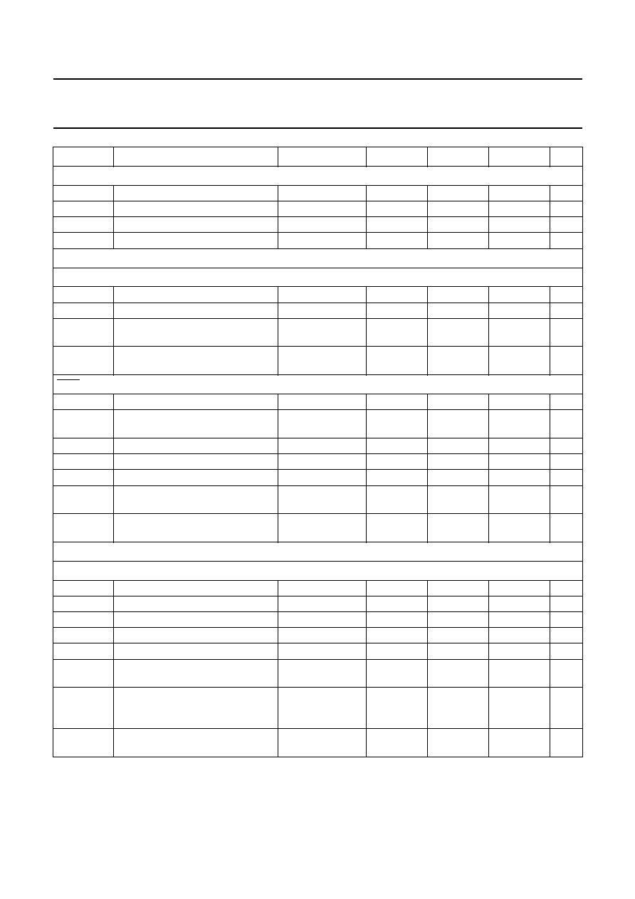
2000 Feb 23
85
Philips Semiconductors
Preliminary specification
Enhanced TV microcontrollers with
On-Screen Display (OSD)
SAA55xx
HSYNC, VSYNC
V
IL
LOW-level input voltage
-
-
0.96
V
V
IH
HIGH-level input voltage
1.80
-
-
V
V
hys
hysteresis of Schmitt trigger input
0.40
-
0.56
V
I
LI
Input leakage current
V
I
= 0 to V
DD
-
-
0.00
µ
A
Digital outputs
FRAME, VDS
V
OL
LOW-level output voltage
I
OL
= 3 mA
-
-
0.13
V
V
OH
HIGH-level output voltage
I
OH
= 3 mA
2.84
-
-
V
t
r
output rise time
10% to 90%;
C
L
= 70 pF
7.50
8.85
10.90
ns
t
f
output fall time
10% to 90%;
C
L
= 70 pF
6.70
7.97
10.00
ns
COR (
OPEN
-
DRAIN OUTPUT
)
V
OL
LOW-level output voltage
I
OL
= 3 mA
-
-
0.14
V
V
OH
HIGH-level pull-up output voltage
I
OL
=
-
3 mA;
push-pull
2.84
-
-
V
V
IL
LOW-level input voltage
-
-
0.00
V
V
IH
HIGH-level input voltage
0.00
-
5.50
V
I
LI
input leakage current
V
I
= 0 to V
DD
-
-
0.12
µ
A
t
r
output rise time
10% to 90%;
C
L
= 70 pF
7.20
8.64
11.10
ns
t
f
output fall time
10% to 90%;
C
L
= 70 pF
4.90
7.34
9.40
ns
Digital input/outputs
P0.0
TO
P0.4, P0.7, P1.0
TO
P1.1, P2.1
TO
P2.7, P3.0
TO
P3.7
V
IL
LOW-level input voltage
-
-
0.98
V
V
IH
HIGH-level input voltage
1.78
-
-
V
V
hys
hysteresis of Schmitt trigger input
0.41
-
0.55
V
I
LI
input leakage current
V
I
= 0 to V
DD
-
-
0.01
µ
A
V
OL
LOW-level output voltage
I
OL
= 4 mA
-
-
0.18
V
V
OH
HIGH-level output voltage
I
OH
=
-
4 mA
push-pull
2.81
-
5.50
V
t
r
output rise time
10% to 90%;
C
L
= 70 pF
push-pull
6.50
8.47
10.70
ns
t
f
output fall time
10% to 90%;
C
L
= 70 pF
5.70
7.56
10.00
ns
SYMBOL
PARAMETER
CONDITIONS
MIN.
TYP.
MAX.
UNIT

2000 Feb 23
86
Philips Semiconductors
Preliminary specification
Enhanced TV microcontrollers with
On-Screen Display (OSD)
SAA55xx
P1.2, P1.3
AND
P2.0
V
IL
LOW-level input voltage
-
-
0.99
V
V
IH
HIGH-level input voltage
1.80
-
-
V
V
hys
hysteresis voltage of Schmitt
trigger input
0.42
-
0.56
V
I
LI
input leakage current
V
I
= 0 to V
DD
-
-
0.02
µ
A
V
OL
LOW-level output voltage
I
OL
= 4 mA
-
-
0.17
V
V
OH
HIGH-level output voltage
I
OH
=
-
4 mA
push-pull
2.81
-
5.50
V
t
r
output rise time
10% to 90%;
C
L
= 70 pF
push-pull
7.00
8.47
10.50
ns
t
f
output fall time
10% to 90%;
C
L
= 70 pF
5.40
7.36
9.30
ns
P0.5
AND
P0.6
V
IL
LOW-level input voltage
-
-
0.98
V
V
IH
HIGH-level input voltage
1.82
-
-
V
I
LI
input leakage current
V
I
= 0 to V
DD
-
-
0.11
µ
A
V
hys
hysteresis voltage of Schmitt
trigger input
0.42
-
0.58
V
V
OL
LOW-level output voltage
I
OL
= 8 mA
-
-
0.20
V
V
OH
HIGH-level output voltage
I
OH
=
-
8 mA
push-pull
2.76
-
5.50
V
t
r
output rise time
10% to 90%;
C
L
= 70 pF
push-pull
7.40
8.22
8.80
ns
t
f
output fall time
10% to 90%;
C
L
= 70 pF
4.20
4.57
5.20
ns
P1.4
TO
P1.7 (
OPEN
-
DRAIN
)
V
IL
LOW-level input voltage
-
-
1.08
V
V
IH
HIGH-level input voltage
1.99
-
-
V
V
hys
hysteresis voltage of Schmitt
trigger input
0.49
-
0.60
V
I
LI
input leakage current
V
I
= 0 to V
DD
-
-
0.13
µ
A
V
OL
LOW-level output voltage
I
OL
= 8 mA
-
-
0.35
V
t
f
output fall time
10% to 90%;
C
L
= 70 pF
69.70
83.67
103.30
ns
SYMBOL
PARAMETER
CONDITIONS
MIN.
TYP.
MAX.
UNIT
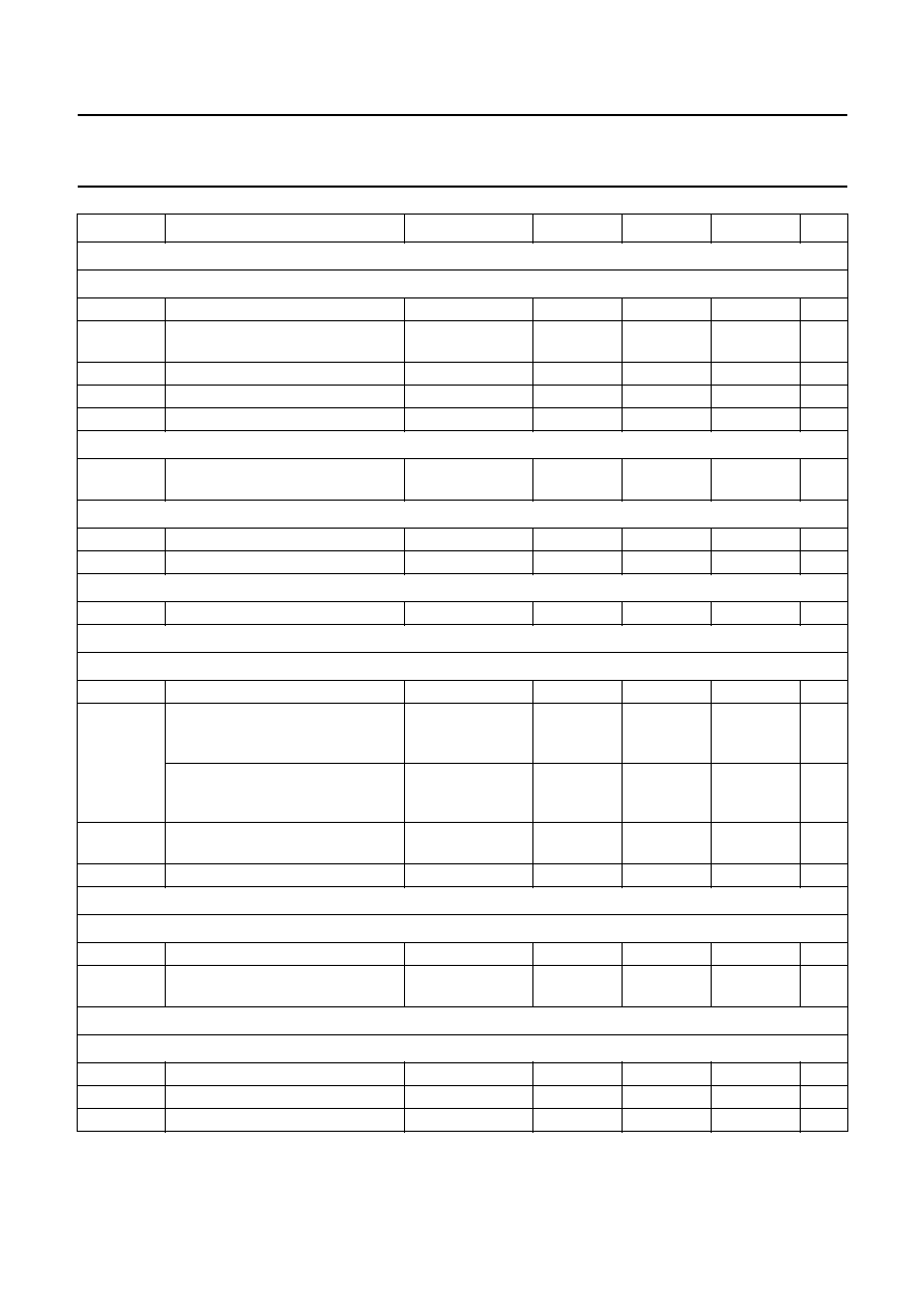
2000 Feb 23
87
Philips Semiconductors
Preliminary specification
Enhanced TV microcontrollers with
On-Screen Display (OSD)
SAA55xx
Analog inputs
CVBS0
AND
CVBS1
V
sync
sync voltage amplitude
0.1
0.3
0.6
V
V
vid(p-p)
video input voltage amplitude
(peak-to-peak value)
0.7
1.0
1.4
V
Z
source
source impedance
0
-
250
V
IH
HIGH-level input voltage
3.0
-
V
DDA
+ 0.3
V
C
I
input capacitance
-
-
10
pF
IREF
R
gnd
resistor to ground
resistor
tolerance 2%
-
24
-
k
ADC0
TO
ADC3
V
IH
HIGH-level input voltage
-
-
V
DDA
V
C
I
input capacitance
-
-
10
pF
VPE
V
IH
HIGH-level input voltage
-
-
9.0
V
Analog outputs
R, G
AND
B
I
OL
Output current (black Level)
V
DDA
= 3.3 V
-
10
-
+10
µ
A
I
OH
Output current (maximum
Intensity)
V
DDA
= 3.3 V
Intensity level
code = 31 dec
6.0
6.67
7.3
mA
Output current (70% of full
Intensity)
V
DDA
= 3.3 V
Intensity level
code = 0 dec
4.2
4.7
5.1
mA
R
load
load resistor to V
SSA
resistor
tolerance 5%
-
150
-
C
L
load capacitance
-
-
15
pF
Analog input/output
SYNC_FILTER
C
sync
storage capacitor to ground
-
100
-
nF
V
sync
sync filter level voltage for nominal
sync amplitude
0.35
0.55
0.75
V
Crystal oscillator
XTALIN
V
IL
LOW-level input voltage
V
SSA
-
-
V
V
IH
HIGH-level input voltage
-
-
V
DDA
V
C
I
input capacitance
-
-
10
pF
SYMBOL
PARAMETER
CONDITIONS
MIN.
TYP.
MAX.
UNIT

2000 Feb 23
88
Philips Semiconductors
Preliminary specification
Enhanced TV microcontrollers with
On-Screen Display (OSD)
SAA55xx
Notes
1. Peripheral current is dependent on external components and voltage levels on I/Os.
2. Crystal order number 4322 143 05561.
3. If the 4322 143 05561 crystal is not used, then the formulae in the crystal specification should be used. Where
C
IO
= 7 pF, the mean of the capacitances due to the chip at XTALIN and at XTALOUT. C
ext
is a value for the mean
of the stray capacitances due to the external circuit at XTALIN and XTALOUT. The maximum value for the crystal
holder capacitance is to ensure start-up, C
osc
may need to be reduced from the initially selected value.
4. C
osc(typ)
= 2C
L
-
C
IO
-
C
ext
5. C
0(max)
= 35
-
1
/
2
(C
osc
+ C
IO
+ C
ext
)
XTALOUT
C
O
output capacitance
-
-
10
pF
Crystal specification; notes 2 and 3
f
xtal
nominal frequency
fundamental
mode
-
12
-
MHz
C
L
crystal load capacitance
-
-
30
pF
C
1
crystal motional capacitance
T
amb
= 25
∞
C
-
-
20
fF
R
r
resonance resistance
T
amb
= 25
∞
C
-
-
60
C
osc
capacitors at XTALIN, XTALOUT
T
amb
= 25
∞
C
-
note 4
-
pF
C
0
crystal holder capacitance
T
amb
= 25
∞
C
-
-
note 5
pF
T
xtal
temperature range
-
20
+25
+85
∞
C
X
j
adjustment tolerance
T
amb
= 25
∞
C
-
-
±
50
◊
10
-
6
X
d
drift
-
-
±
100
◊
10
-
6
SYMBOL
PARAMETER
CONDITIONS
MIN.
TYP.
MAX.
UNIT

2000 Feb 23
89
Philips Semiconductors
Preliminary specification
Enhanced TV microcontrollers with
On-Screen Display (OSD)
SAA55xx
Table 35 I
2
C-bus characteristics
Notes
1. A device must internally provide a hold time of at least 300 ns for the SDA signal (referred to the V
IL(min)
of the SCL
signal) in order to bridge the undefined region of the falling edge of SCL.
2. The maximum f
HD;DAT
has only to be met if the device does not stretch the LOW period t
LOW
of the SCL signal.
3. A fast-mode I
2
C-bus device can be used in a standard mode I
2
C-bus system but the requirement t
SU;DAT
250 ns
must then be met. This will automatically be the case if the device does not stretch the LOW period of the SCL signal.
If such a device does stretch the LOW period of the SCL signal, it must output the next data bit to the SDA line
t
r(max)
+ t
SU;DAT
= 1000 + 250 +1250 ns (according to the standard mode I
2
C-bus specification) before the SCL line
is released.
4. C
b
= total capacitance of one bus line in pF.
SYMBOL
PARAMETER
FAST-MODE I
2
C-bus
UNIT
MIN.
MAX.
f
SCL
SCL clock frequency
0
400
kHz
t
BUF
bus free time between a STOP and START condition
1.3
-
µ
s
t
HD;STA
hold time (repeated) START condition. After this period, the
first clock pulse is generated.
0.6
-
µ
s
t
LOW
LOW period of the SCL clock
1.3
-
µ
s
t
HIGH
HIGH period of the SCL clock
0.6
-
µ
s
t
SU;STA
set-up time for a repeated START condition
0.6
-
µ
s
t
HD;DAT
data hold time; notes 1 and 2
0
0.9
µ
s
t
SU;DAT
data set-up time, note 3
100
-
ns
t
r
rise time of both SDA and SCL signals; note 4
20
300
ns
t
f
fall time of both SDA and SCL signals; note 4
20
300
ns
t
SU;STO
set-up time for STOP condition
0.6
-
µ
s
C
b
capacitive load for each bus line
-
400
pF
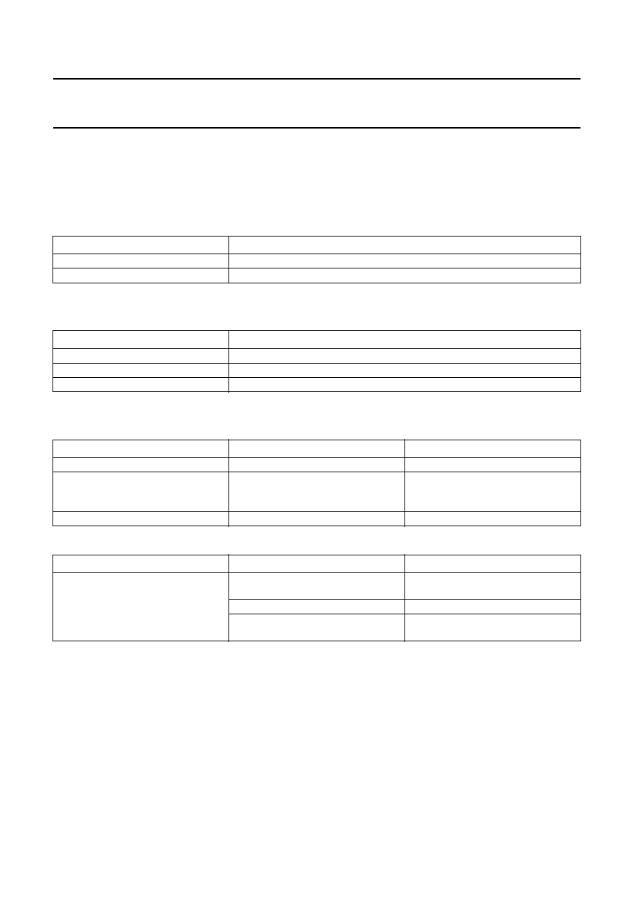
2000 Feb 23
90
Philips Semiconductors
Preliminary specification
Enhanced TV microcontrollers with
On-Screen Display (OSD)
SAA55xx
23 QUALITY AND RELIABILITY
This device will meet Philips Semiconductors General Quality Specification for Business group
"Consumer Integrated
Circuits SNW-FQ-611-Part E". The principal requirements are shown in Tables 36 to 39.
23.1
Group A
Table 36 Acceptance tests per lot
23.2
Group B
Table 37 Processability tests (by package family)
23.3
Group C
Table 38 Reliability tests (by process family)
Table 39 Reliability tests (by device type)
Notes to Tables 36 to 39
1. ppm = fraction of defective devices, in parts per million.
2. FPM = fraction of devices failing at test condition, in Failures Per Million.
TEST
REQUIREMENTS
Mechanical
cumulative target: <80 ppm
Electrical
cumulative target: <100 ppm
TEST
REQUIREMENTS
Solderability
0/16 on all lots
Mechanical
0/15 on all lots
Solder heat resistance
0/15 on all lots
TEST
CONDITIONS
REQUIREMENTS
Operational life
168 hours at T
j
= 150
∞
C
<1000 FPM at T
j
= 150
∞
C
Humidity life
temperature, humidity, bias
1000 hours, 85
∞
C, 85% RH
(or equivalent test)
<2000 FPM
Temperature cycling performance
T
stg(min)
to T
stg(max)
<2000 FPM
TEST
CONDITIONS
REQUIREMENTS
ESD and latch-up
ESD Human body model 100 pF,
1.5 k
2000 V
ESD Machine model 200 pF, 0
200 V
latch-up
100 mA, 1.5
◊
V
DD
(absolute
maximum)
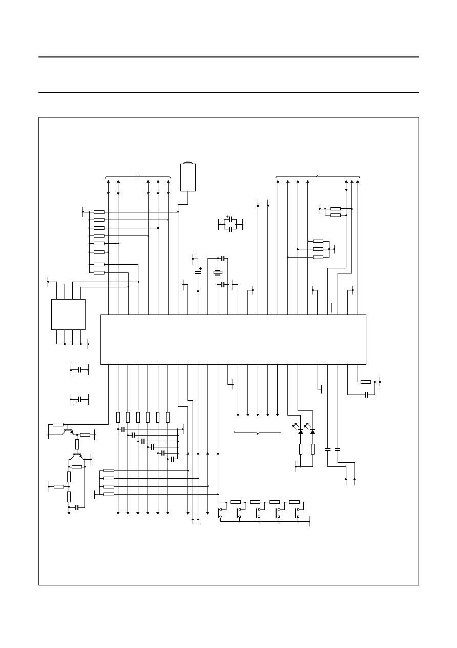
2000
Feb
23
91
Philips Semiconductors
Preliminar
y specification
Enhanced TV microcontrollers with
On-Screen Displa
y (OSD)
SAA55xx
This text is here in white to force landscape pages to be rotated correctly when browsing through the pdf in the Acrobat reader.This text is here in
_
white to force landscape pages to be rotated correctly when browsing through the pdf in the Acrobat reader.This text is here inThis text is here in
white to force landscape pages to be rotated correctly when browsing through the pdf in the Acrobat reader. white to force landscape pages to be ...
24
APPLICA
TION INFORMA
TION
o
k, full pagewidth
MBK980
2
VDD
VDD
VAFC
AV status
program
+
program
-
plus(
+
)
minus(
-
)
menu
Vtune
VSS
VSS
VSS
VDD
VDD
VDD
VDD
VSSC
VDDP
VDDC
VSSP
VSSA
VSS
VPE
VSS
VSS
VSS
P2.1/PWM0
3
P2.2/PWM1
4
P2.3/PWM2
5
P2.4/PWM3
6
P2.5/PWM4
7
P2.6/PWM5
8
P2.7/PWM6
9
P3.0/ADC0
P3.1/ADC1
P3.2/ADC2
P0.0
VHF-L
VHF-H
UHF
TV control
signals
P3.3/ADC3
10
11
12
13
14
15
16
17
18
19
20
21
P0.1
P0.2
P0.3
P0.4
P0.5
P0.6
P0.7
G
B
VDDA
HSYNC
VDS
R
VSYNC
XTALOUT
XTALIN
OSCGND
P1.0/INT1
RESET
P3.4/PWM7
IREF
100 nF
100 nF
100 nF
FRAME
SYNC_FILTER
CVBS1
CVBS0
CVBS (IF)
CVBS (SCART)
22
23
24
26
25
29
27
28
1
51
50
49
48
47
46
45
44
43
42
41
40
39
38
37
36
35
34
33
32
31
30
52
P2.0/TPWM
A2
P1.4/SCL1
P1.7/SDA0
P1.6/SCL0
P1.3/T1
P1.2/INT0
P1.1/T0
P1.5/SDA1
SDA
A1
SCL
A0
RC
brightness
contrast
saturation
hue
volume (L)
volume (R)
VDD
VSS
1 k
1 k
150
24 k
VDD
40 V
VSS
VSS
VDD
VSS
PH2369
47
µ
F
VDD
VSS
100 nF
COR
VSS
VDD
47
µ
F
10
µ
F
100 nF
56 pF
VDD
VDD
VDD
VSS
VSS
EEPROM
PCF8582E
SAA55xx
IR
RECEIVER
12 MHz
to TV's
display
circuits
TV
control
signals
field flyback
line flyback
Fig.40 Application diagram.
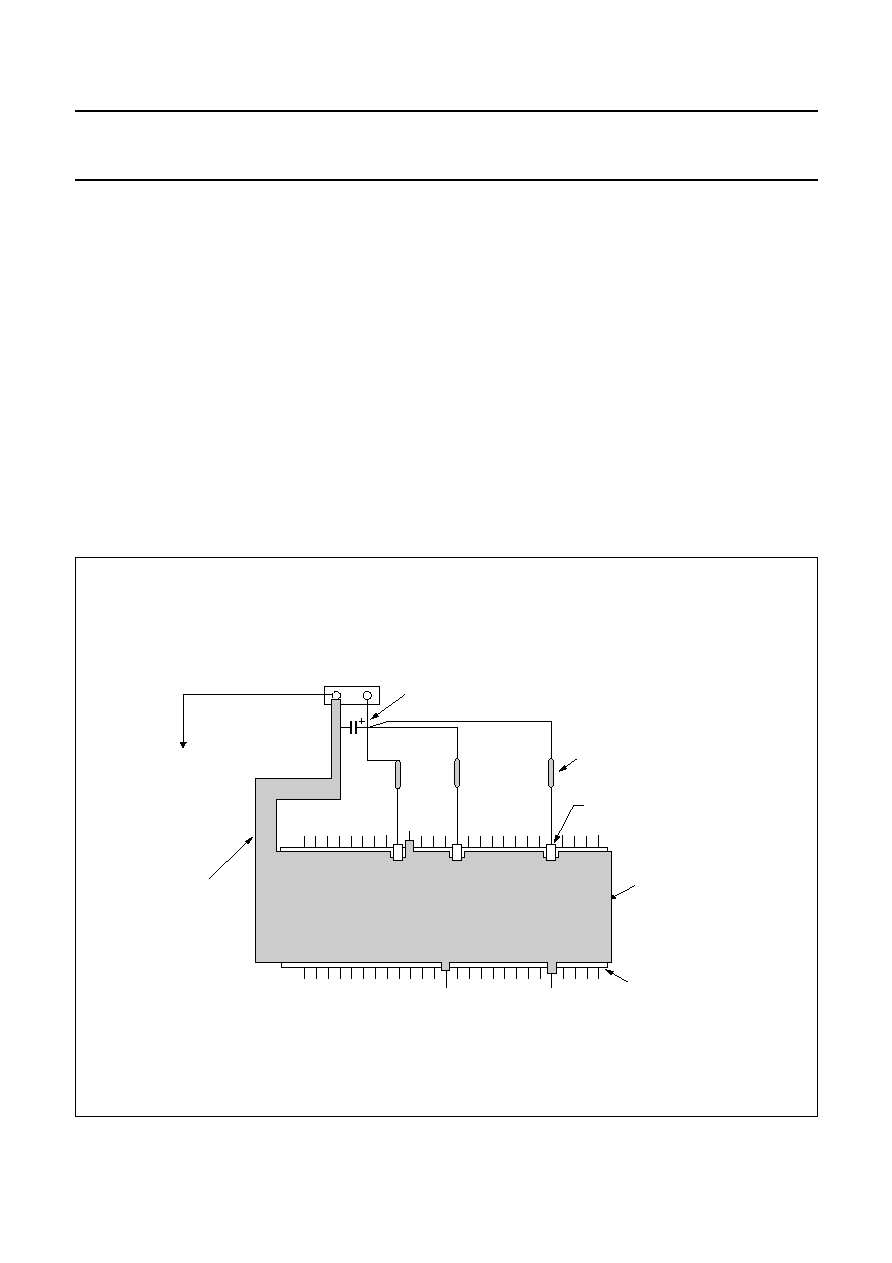
2000 Feb 23
92
Philips Semiconductors
Preliminary specification
Enhanced TV microcontrollers with
On-Screen Display (OSD)
SAA55xx
25 EMC GUIDELINES
Optimization of circuit return paths and minimisation of
common mode emission will be assisted by using a double
sided printed-circuit board (PCB) with low inductance
ground plane.
On a single sided PCB local ground plane under the
whole IC should be present as shown in Fig.41. This
should be connected by the widest possible connection
back to the PCB ground connection, and bulk electrolytic
decoupling capacitor. It should preferably not connect to
other grounds on the way and no wire links should be
present in this connect. The use of wire links increases
ground bounce by introducing inductance into the ground.
The supply pins can be decoupled at the pin to the ground
plane under the IC. This is easily accomplished using
surface mount capacitors, which are more effective than
leaded components at high frequency.
Using a device socket will unfortunately add to the area
and inductance of the external bypass loop.
A ferrite bead or inductor with resistive characteristics at
high frequencies may be utilised in the supply line close to
the decoupling capacitor to provide a high-impedance.
To prevent pollution by conduction onto the signal lines
(which may then radiate) signals connected to the V
DD
supply via a pull-up resistor should not be connected to the
IC side of this ferrite component.
OSCGND should be connected only to the crystal load
capacitors and not the local or circuit GND.
Physical connection distances to associated active
devices should be short.
Output traces should be routed with close proximity to
mutually coupled ground return paths.
Fig.41 Power supply connections for EMC.
handbook, full pagewidth
electrolytic decoupling capacitor (2
µ
F)
ferrite beads
SM decoupling capacitors (10 to 100 nF)
under-IC GND plane
IC
MBK979
VSSC
VSSA
V
DDP
V
SSP
V
DDC
V
DDA
GND
+
3.3 V
other
GND
connections
under-IC GND plane
GND connection
note: no wire links

2000 Feb 23
93
Philips Semiconductors
Preliminary specification
Enhanced TV microcontrollers with
On-Screen Display (OSD)
SAA55xx
26 REFERENCES
1. 80C51 Based 8-Bit Microcontrollers. Philips Semiconductors (ref. IC20).
2. The I
2
C-bus and how to use it (including specification). Philips Semiconductors.
3. Enhanced Teletext Specification European Telecommunication Standard ETS 300 706.
4. World System Teletext and Data Broadcasting System. DTI. December 1987 (525 WST only).
5. Specification of the Domestic Video Programme Delivery Control System (PDC); EBU Tech. 3262-E.
6. Recommended Practise for Line 21 Data Service EIA-608.
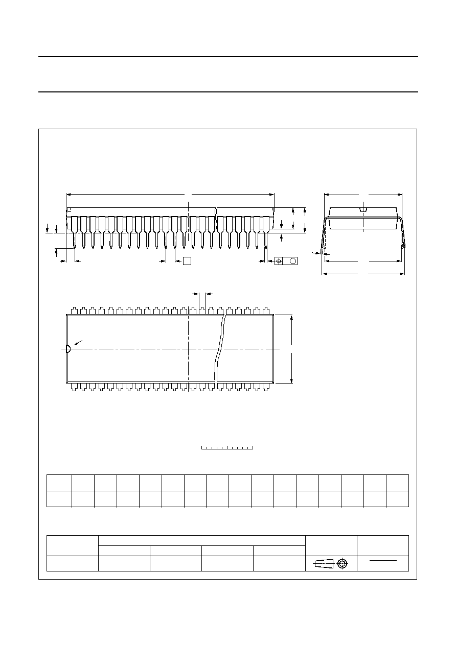
2000 Feb 23
94
Philips Semiconductors
Preliminary specification
Enhanced TV microcontrollers with
On-Screen Display (OSD)
SAA55xx
27 PACKAGE OUTLINES
UNIT
b
1
c
E
e
M
H
L
REFERENCES
OUTLINE
VERSION
EUROPEAN
PROJECTION
ISSUE DATE
IEC
JEDEC
EIAJ
mm
DIMENSIONS (mm are the original dimensions)
SOT247-1
95-03-11
99-12-27
b
max.
w
M
E
e
1
1.3
0.8
0.53
0.40
0.32
0.23
47.9
47.1
14.0
13.7
3.2
2.8
0.18
1.778
15.24
15.80
15.24
17.15
15.90
1.73
5.08
0.51
4.0
MS-020
M
H
c
(e )
1
M
E
A
L
seating plane
A
1
w
M
b
1
D
A
2
Z
52
1
27
26
b
E
pin 1 index
0
5
10 mm
scale
Note
1. Plastic or metal protrusions of 0.25 mm maximum per side are not included.
(1)
(1)
D
(1)
Z
e
A
max.
1
2
A
min.
A
max.
SDIP52: plastic shrink dual in-line package; 52 leads (600 mil)
SOT247-1
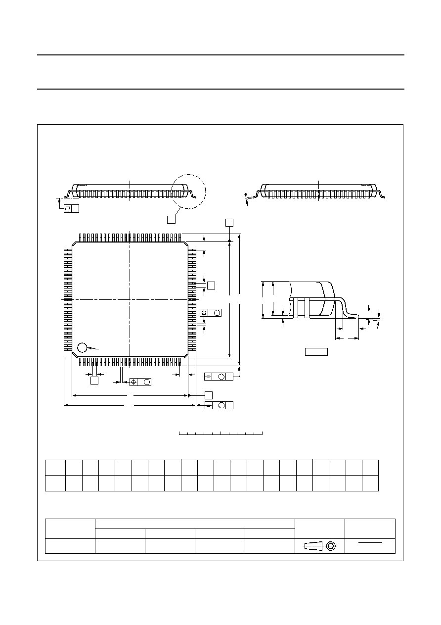
2000 Feb 23
95
Philips Semiconductors
Preliminary specification
Enhanced TV microcontrollers with
On-Screen Display (OSD)
SAA55xx
UNIT
A
max.
A
1
A
2
A
3
b
p
c
E
(1)
e
H
E
L
L
p
Z
y
w
v
REFERENCES
OUTLINE
VERSION
EUROPEAN
PROJECTION
ISSUE DATE
IEC
JEDEC
EIAJ
mm
1.6
0.15
0.05
1.45
1.35
0.25
0.27
0.17
0.20
0.09
14.1
13.9
0.5
16.25
15.75
1.15
0.85
7
0
o
o
0.08
0.08
0.2
1.0
DIMENSIONS (mm are the original dimensions)
Note
1. Plastic or metal protrusions of 0.25 mm maximum per side are not included.
0.75
0.45
SOT407-1
136E20
MS-026
00-01-19
00-02-01
D
(1)
(1)
(1)
14.1
13.9
H
D
16.25
15.75
E
Z
1.15
0.85
D
b
p
e
E
A
1
A
L
p
detail X
L
(A )
3
B
25
c
D
H
b
p
E
H
A
2
v
M
B
D
ZD
A
Z E
e
v
M
A
X
1
100
76
75
51
50
26
y
pin 1 index
w
M
w
M
0
5
10 mm
scale
LQFP100: plastic low profile quad flat package; 100 leads; body 14 x 14 x 1.4 mm
SOT407-1

2000 Feb 23
96
Philips Semiconductors
Preliminary specification
Enhanced TV microcontrollers with
On-Screen Display (OSD)
SAA55xx
28 SOLDERING
28.1
Introduction to soldering through-hole mount
packages
This text gives a brief insight to wave, dip and manual
soldering. A more in-depth account of soldering ICs can be
found in our
"Data Handbook IC26; Integrated Circuit
Packages" (document order number 9398 652 90011).
Wave soldering is the preferred method for mounting of
through-hole mount IC packages on a printed-circuit
board.
28.2
Soldering by dipping or by solder wave
The maximum permissible temperature of the solder is
260
∞
C; solder at this temperature must not be in contact
with the joints for more than 5 seconds.
The total contact time of successive solder waves must not
exceed 5 seconds.
The device may be mounted up to the seating plane, but
the temperature of the plastic body must not exceed the
specified maximum storage temperature (T
stg(max)
). If the
printed-circuit board has been pre-heated, forced cooling
may be necessary immediately after soldering to keep the
temperature within the permissible limit.
28.3
Manual soldering
Apply the soldering iron (24 V or less) to the lead(s) of the
package, either below the seating plane or not more than
2 mm above it. If the temperature of the soldering iron bit
is less than 300
∞
C it may remain in contact for up to
10 seconds. If the bit temperature is between
300 and 400
∞
C, contact may be up to 5 seconds.
28.4
Suitability of through-hole mount IC packages for dipping and wave soldering methods
Note
1. For SDIP packages, the longitudinal axis must be parallel to the transport direction of the printed-circuit board.
PACKAGE
SOLDERING METHOD
DIPPING
WAVE
DBS, DIP, HDIP, SDIP, SIL
suitable
suitable
(1)

2000 Feb 23
97
Philips Semiconductors
Preliminary specification
Enhanced TV microcontrollers with
On-Screen Display (OSD)
SAA55xx
29 DEFINITIONS
30 LIFE SUPPORT APPLICATIONS
These products are not designed for use in life support appliances, devices, or systems where malfunction of these
products can reasonably be expected to result in personal injury. Philips customers using or selling these products for
use in such applications do so at their own risk and agree to fully indemnify Philips for any damages resulting from such
improper use or sale.
31 PURCHASE OF PHILIPS I
2
C COMPONENTS
Data sheet status
Objective specification
This data sheet contains target or goal specifications for product development.
Preliminary specification
This data sheet contains preliminary data; supplementary data may be published later.
Product specification
This data sheet contains final product specifications.
Limiting values
Limiting values given are in accordance with the Absolute Maximum Rating System (IEC 134). Stress above one or
more of the limiting values may cause permanent damage to the device. These are stress ratings only and operation
of the device at these or at any other conditions above those given in the Characteristics sections of the specification
is not implied. Exposure to limiting values for extended periods may affect device reliability.
Application information
Where application information is given, it is advisory and does not form part of the specification.
Purchase of Philips I
2
C components conveys a license under the Philips' I
2
C patent to use the
components in the I
2
C system provided the system conforms to the I
2
C specification defined by
Philips. This specification can be ordered using the code 9398 393 40011.

2000 Feb 23
98
Philips Semiconductors
Preliminary specification
Enhanced TV microcontrollers with
On-Screen Display (OSD)
SAA55xx
NOTES

2000 Feb 23
99
Philips Semiconductors
Preliminary specification
Enhanced TV microcontrollers with
On-Screen Display (OSD)
SAA55xx
NOTES

© Philips Electronics N.V.
SCA
All rights are reserved. Reproduction in whole or in part is prohibited without the prior written consent of the copyright owner.
The information presented in this document does not form part of any quotation or contract, is believed to be accurate and reliable and may be changed
without notice. No liability will be accepted by the publisher for any consequence of its use. Publication thereof does not convey nor imply any license
under patent- or other industrial or intellectual property rights.
Internet: http://www.semiconductors.philips.com
2000
69
Philips Semiconductors ≠ a worldwide company
For all other countries apply to: Philips Semiconductors,
International Marketing & Sales Communications, Building BE-p, P.O. Box 218,
5600 MD EINDHOVEN, The Netherlands, Fax. +31 40 27 24825
Argentina: see South America
Australia: 3 Figtree Drive, HOMEBUSH, NSW 2140,
Tel. +61 2 9704 8141, Fax. +61 2 9704 8139
Austria: Computerstr. 6, A-1101 WIEN, P.O. Box 213,
Tel. +43 1 60 101 1248, Fax. +43 1 60 101 1210
Belarus: Hotel Minsk Business Center, Bld. 3, r. 1211, Volodarski Str. 6,
220050 MINSK, Tel. +375 172 20 0733, Fax. +375 172 20 0773
Belgium: see The Netherlands
Brazil: see South America
Bulgaria: Philips Bulgaria Ltd., Energoproject, 15th floor,
51 James Bourchier Blvd., 1407 SOFIA,
Tel. +359 2 68 9211, Fax. +359 2 68 9102
Canada: PHILIPS SEMICONDUCTORS/COMPONENTS,
Tel. +1 800 234 7381, Fax. +1 800 943 0087
China/Hong Kong: 501 Hong Kong Industrial Technology Centre,
72 Tat Chee Avenue, Kowloon Tong, HONG KONG,
Tel. +852 2319 7888, Fax. +852 2319 7700
Colombia: see South America
Czech Republic: see Austria
Denmark: Sydhavnsgade 23, 1780 COPENHAGEN V,
Tel. +45 33 29 3333, Fax. +45 33 29 3905
Finland: Sinikalliontie 3, FIN-02630 ESPOO,
Tel. +358 9 615 800, Fax. +358 9 6158 0920
France: 51 Rue Carnot, BP317, 92156 SURESNES Cedex,
Tel. +33 1 4099 6161, Fax. +33 1 4099 6427
Germany: Hammerbrookstraþe 69, D-20097 HAMBURG,
Tel. +49 40 2353 60, Fax. +49 40 2353 6300
Hungary: see Austria
India: Philips INDIA Ltd, Band Box Building, 2nd floor,
254-D, Dr. Annie Besant Road, Worli, MUMBAI 400 025,
Tel. +91 22 493 8541, Fax. +91 22 493 0966
Indonesia: PT Philips Development Corporation, Semiconductors Division,
Gedung Philips, Jl. Buncit Raya Kav.99-100, JAKARTA 12510,
Tel. +62 21 794 0040 ext. 2501, Fax. +62 21 794 0080
Ireland: Newstead, Clonskeagh, DUBLIN 14,
Tel. +353 1 7640 000, Fax. +353 1 7640 200
Israel: RAPAC Electronics, 7 Kehilat Saloniki St, PO Box 18053,
TEL AVIV 61180, Tel. +972 3 645 0444, Fax. +972 3 649 1007
Italy: PHILIPS SEMICONDUCTORS, Via Casati, 23 - 20052 MONZA (MI),
Tel. +39 039 203 6838, Fax +39 039 203 6800
Japan: Philips Bldg 13-37, Kohnan 2-chome, Minato-ku,
TOKYO 108-8507, Tel. +81 3 3740 5130, Fax. +81 3 3740 5057
Korea: Philips House, 260-199 Itaewon-dong, Yongsan-ku, SEOUL,
Tel. +82 2 709 1412, Fax. +82 2 709 1415
Malaysia: No. 76 Jalan Universiti, 46200 PETALING JAYA, SELANGOR,
Tel. +60 3 750 5214, Fax. +60 3 757 4880
Mexico: 5900 Gateway East, Suite 200, EL PASO, TEXAS 79905,
Tel. +9-5 800 234 7381, Fax +9-5 800 943 0087
Middle East: see Italy
Netherlands: Postbus 90050, 5600 PB EINDHOVEN, Bldg. VB,
Tel. +31 40 27 82785, Fax. +31 40 27 88399
New Zealand: 2 Wagener Place, C.P.O. Box 1041, AUCKLAND,
Tel. +64 9 849 4160, Fax. +64 9 849 7811
Norway: Box 1, Manglerud 0612, OSLO,
Tel. +47 22 74 8000, Fax. +47 22 74 8341
Pakistan: see Singapore
Philippines: Philips Semiconductors Philippines Inc.,
106 Valero St. Salcedo Village, P.O. Box 2108 MCC, MAKATI,
Metro MANILA, Tel. +63 2 816 6380, Fax. +63 2 817 3474
Poland: Al.Jerozolimskie 195 B, 02-222 WARSAW,
Tel. +48 22 5710 000, Fax. +48 22 5710 001
Portugal: see Spain
Romania: see Italy
Russia: Philips Russia, Ul. Usatcheva 35A, 119048 MOSCOW,
Tel. +7 095 755 6918, Fax. +7 095 755 6919
Singapore: Lorong 1, Toa Payoh, SINGAPORE 319762,
Tel. +65 350 2538, Fax. +65 251 6500
Slovakia: see Austria
Slovenia: see Italy
South Africa: S.A. PHILIPS Pty Ltd., 195-215 Main Road Martindale,
2092 JOHANNESBURG, P.O. Box 58088 Newville 2114,
Tel. +27 11 471 5401, Fax. +27 11 471 5398
South America: Al. Vicente Pinzon, 173, 6th floor,
04547-130 S√O PAULO, SP, Brazil,
Tel. +55 11 821 2333, Fax. +55 11 821 2382
Spain: Balmes 22, 08007 BARCELONA,
Tel. +34 93 301 6312, Fax. +34 93 301 4107
Sweden: Kottbygatan 7, Akalla, S-16485 STOCKHOLM,
Tel. +46 8 5985 2000, Fax. +46 8 5985 2745
Switzerland: Allmendstrasse 140, CH-8027 ZÐRICH,
Tel. +41 1 488 2741 Fax. +41 1 488 3263
Taiwan: Philips Semiconductors, 6F, No. 96, Chien Kuo N. Rd., Sec. 1,
TAIPEI, Taiwan Tel. +886 2 2134 2886, Fax. +886 2 2134 2874
Thailand: PHILIPS ELECTRONICS (THAILAND) Ltd.,
209/2 Sanpavuth-Bangna Road Prakanong, BANGKOK 10260,
Tel. +66 2 745 4090, Fax. +66 2 398 0793
Turkey: Yukari Dudullu, Org. San. Blg., 2.Cad. Nr. 28 81260 Umraniye,
ISTANBUL, Tel. +90 216 522 1500, Fax. +90 216 522 1813
Ukraine: PHILIPS UKRAINE, 4 Patrice Lumumba str., Building B, Floor 7,
252042 KIEV, Tel. +380 44 264 2776, Fax. +380 44 268 0461
United Kingdom: Philips Semiconductors Ltd., 276 Bath Road, Hayes,
MIDDLESEX UB3 5BX, Tel. +44 208 730 5000, Fax. +44 208 754 8421
United States: 811 East Arques Avenue, SUNNYVALE, CA 94088-3409,
Tel. +1 800 234 7381, Fax. +1 800 943 0087
Uruguay: see South America
Vietnam: see Singapore
Yugoslavia: PHILIPS, Trg N. Pasica 5/v, 11000 BEOGRAD,
Tel. +381 11 3341 299, Fax.+381 11 3342 553
Printed in The Netherlands
753504/02/pp
100
Date of release:
2000 Feb 23
Document order number:
9397 750 06787