2004 Mar 04
2
Philips Semiconductors
Product specification
Digital video encoder
SAA7104H; SAA7105H
CONTENTS
1
FEATURES
2
GENERAL DESCRIPTION
3
QUICK REFERENCE DATA
4
ORDERING INFORMATION
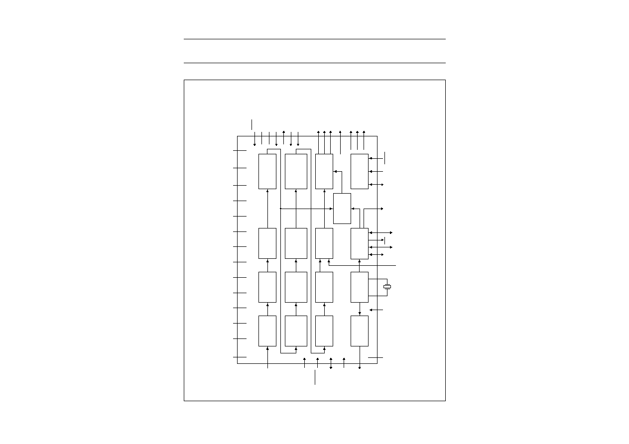
5
BLOCK DIAGRAM
6
PINNING
7
FUNCTIONAL DESCRIPTION
7.1
Reset conditions
7.2
Input formatter
7.3
RGB LUT
7.4
Cursor insertion
7.5
RGB Y-C
B
-C
R
matrix
7.6
Horizontal scaler
7.7
Vertical scaler and anti-flicker filter
7.8
FIFO
7.9
Border generator
7.10
Oscillator and Discrete Time Oscillator (DTO)
7.11
Low-pass Clock Generation Circuit (CGC)
7.12
Encoder
7.13
RGB processor
7.14
Triple DAC
7.15
HD data path
7.16
Timing generator
7.17
Pattern generator for HD sync pulses
7.18
I
2
C-bus interface
7.19
Power-down modes
7.20
Programming the SAA7104H; SAA7105H
7.21
Input levels and formats
7.22
Bit allocation map
7.23
I
2
C-bus format
7.24
Slave receiver
7.25
Slave transmitter
8
BOUNDARY SCAN TEST
8.1
Initialization of boundary scan circuit
8.2
Device identification codes
9
LIMITING VALUES
10
THERMAL CHARACTERISTICS
11
CHARACTERISTICS
11.1
Teletext timing
12
APPLICATION INFORMATION
12.1
Reconstruction filter
12.2
Analog output voltages
12.3
Suggestions for a board layout
13
PACKAGE OUTLINE
14
SOLDERING
14.1
Introduction to soldering surface mount
packages
14.2
Reflow soldering
14.3
Wave soldering
14.4
Manual soldering
14.5
Suitability of surface mount IC packages for
wave and reflow soldering methods
15
DATA SHEET STATUS
16
DEFINITIONS
17
DISCLAIMERS
18
PURCHASE OF PHILIPS I
2
C COMPONENTS
2004 Mar 04
3
Philips Semiconductors
Product specification
Digital video encoder
SAA7104H; SAA7105H
1
FEATURES
�
Digital PAL/NTSC encoder with integrated high quality
scaler and anti-flicker filter for TV output from a PC
�
Supports Intel
�
Digital Video Out (DVO) low voltage
interfacing to graphics controller
�
27 MHz crystal-stable subcarrier generation
�
Maximum graphics pixel clock 85 MHz at double edged
clocking, synthesized on-chip or from external source
�
Programmable assignment of clock edge to bytes (in
double edged mode)
�
Synthesizable pixel clock (PIXCLK) with minimized
output jitter, can be used as reference clock for the VGC,
as well)
�
PIXCLK output and bi-phase PIXCLK input (VGC clock
loop-through possible)
�
Hot-plug detection through dedicated interrupt pin
�
Supported VGA resolutions for PAL or NTSC legacy
video output up to 1280
�
1024 graphics data at
60 or 50 Hz frame rate
�
Supported VGA resolutions for HDTV output up to
1920
�
1080 interlaced graphics data at 60 or 50 Hz
frame rate
�
Three Digital-to-Analog Converters (DACs) for CVBS
(BLUE, C
B
), VBS (GREEN, CVBS) and C (RED, C
R
) at
27 MHz sample rate (signals in parenthesis are
optionally), all at 10-bit resolution
�
Non-interlaced C
B
-Y-C
R
or RGB input at maximum
4 : 4 : 4 sampling
�
Downscaling and upscaling from 50 to 400%
�
Optional interlaced C
B
-Y-C
R
input of Digital Versatile
Disk (DVD) signals
�
Optional non-interlaced RGB output to drive second
VGA monitor (bypass mode, maximum 85 MHz)
�
3
�
256 bytes RGB Look-Up Table (LUT)
�
Support for hardware cursor
�
HDTV up to 1920
�
1080 interlaced and 1280
�
720
progressive, including 3-level sync pulses
�
Programmable border colour of underscan area
�
Programmable 5 line anti-flicker filter
�
On-chip 27 MHz crystal oscillator (3rd-harmonic or
fundamental 27 MHz crystal)
�
Fast I
2
C-bus control port (400 kHz)
�
Encoder can be master or slave
�
Adjustable output levels for the DACs
�
Programmable horizontal and vertical input
synchronization phase
�
Programmable horizontal sync output phase
�
Internal Colour Bar Generator (CBG)
�
Optional support of various Vertical Blanking Interval
(VBI) data insertion
�
Macrovision
TM
(1)
Pay-per-View copy protection system
rev. 7.01, rev. 6.1 and rev. 1.03 (525p) as option; this
applies to the SAA7104H only. The device is protected
by USA patent numbers 4631603, 4577216 and
4819098 and other intellectual property rights. Use of
the Macrovision anti-copy process in the device is
licensed for non-commercial home use only. Reverse
engineering or disassembly is prohibited. Please
contact your nearest Philips Semiconductors sales
office for more information.
�
Optional cross-colour reduction for PAL and NTSC
CVBS outputs
�
Power-save modes
�
Joint Test Action Group (JTAG) boundary scan test
�
Monolithic CMOS 3.3 V device, 5 V tolerant I/Os
�
QFP64 package.
(1) Macrovision
TM
is a trademark of the Macrovision Corporation.

2004 Mar 04
4
Philips Semiconductors
Product specification
Digital video encoder
SAA7104H; SAA7105H
2
GENERAL DESCRIPTION
The SAA7104H; SAA7105H is an advanced
next-generation video encoder which converts PC
graphics data at maximum 1280
�
1024 resolution
(optionally 1920
�
1080 interlaced) to PAL (50 Hz) or
NTSC (60 Hz) video signals. A programmable scaler and
anti-flicker filter (maximum 5 lines) ensures properly sized
and flicker-free TV display as CVBS or S-video output.
Alternatively, the three Digital-to-Analog Converters
(DACs) can output RGB signals together with a TTL
composite sync to feed SCART connectors.
When the scaler/interlacer is bypassed, a second VGA
monitor can be connected to the RGB outputs and
separate H and V-syncs as well, thereby serving as an
auxiliary monitor at maximum 1280
�
1024
resolution/60 Hz (PIXCLK < 85 MHz). Alternatively this
port can provide Y, P
B
and P
R
signals for HDTV monitors.
The device includes a sync/clock generator and on-chip
DACs.
All inputs intended to interface to the host graphics
controller are designed for low-voltage signals between
down to 1.1 V and up to 3.6 V.
3
QUICK REFERENCE DATA
4
ORDERING INFORMATION
SYMBOL
PARAMETER
MIN.
TYP.
MAX.
UNIT
V
DDA
analog supply voltage
3.15
3.3
3.45
V
V
DDD
digital supply voltage
3.15
3.3
3.45
V
I
DDA
analog supply current
1
110
115
mA
I
DDD
digital supply current
1
175
200
mA
V
i
input signal voltage levels
TTL compatible
V
o(p-p)
analog CVBS output signal voltage for a 100/100
colour bar at 75/2
load (peak-to-peak value)
-
1.23
-
V
R
L
load resistance
-
37.5
-
ILE
lf(DAC)
low frequency integral linearity error of DACs
-
-
�
3
LSB
DLE
lf(DAC)
low frequency differential linearity error of DACs
-
-
�
1
LSB
T
amb
ambient temperature
0
-
70
�
C
TYPE NUMBER
PACKAGE
NAME
DESCRIPTION
VERSION
SAA7104H
QFP64
plastic quad flat package; 64 leads (lead length 1.6 mm);
body 14
�
14
�
2.7 mm
SOT393-1
SAA7105H