Document Outline
- 1 FEATURES
- 2 APPLICATIONS
- 3 GENERAL DESCRIPTION
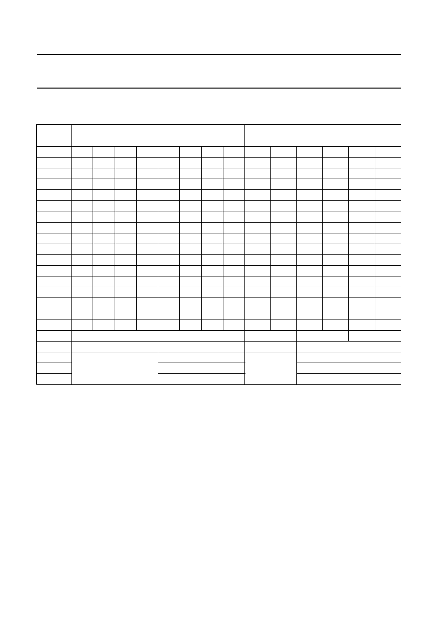
- 4 QUICK REFERENCE DATA
- 5 ORDERING INFORMATION
- 6 SYSTEM VIEW
- 7 BLOCK DIAGRAM
- 8 PINNING
- 9 FUNCTIONAL DESCRIPTION
- 9.1 Analog input processing
- 9.2 Analog control circuits
- 9.3 Chrominance processing
- 9.4 Luminance processing
- 9.5 YUV-bus (digital outputs)
- 9.6 Synchronization
- 9.7 Clock generation circuit
- 9.8 Power-on reset
- 9.9 RTCO output
- 10 GAIN CHARTS
- 11 LIMITING VALUES
- 12 CHARACTERISTICS
- 13 TIMING
- 14 OUTPUT FORMATS
- 15 CLOCK SYSTEM
- 15.1 Clock generation circuit
- 15.2 Power-on control
- 16 I2C-BUS DESCRIPTION
- 16.1 I2C-bus format
- 16.2I2 C-bus receiver/transmitter tables
- 16.3 I2C-bus detail
- 16.4 I2C-bus detail
- 17 SOURCE SELECTION MANAGEMENT
- 18 ANTI-ALIAS FILTER GRAPHS
- 19 CORING FUNCTION
- 19.1 Coring function adjustment by subaddress 06H to affect band filter output adjustment
- 20 LUMINANCE FILTER GRAPHS
- 21 I2C-BUS START SET-UP
- 22 APPLICATION INFORMATION
- 23 START-UP, SOURCE SELECT AND STANDARD DETECTION FLOW EXAMPLE
- 24 PACKAGE OUTLINE
- 25 SOLDERING
- 25.1 Introduction
- 25.2 Reflow soldering
- 25.3 Wave soldering
- 25.4 Repairing soldered joints
- 26 DEFINITIONS
- 27 LIFE SUPPORT APPLICATIONS
- 28 PURCHASE OF PHILIPS I2C COMPONENTS

DATA SHEET
Product specification
File under Integrated Circuits, IC22
1995 Oct 18
INTEGRATED CIRCUITS
SAA7110; SAA7110A
One Chip Front-end 1 (OCF1)

1995 Oct 18
2
Philips Semiconductors
Product specification
One Chip Front-end 1 (OCF1)
SAA7110; SAA7110A
CONTENTS
1
FEATURES
2
APPLICATIONS
3
GENERAL DESCRIPTION
4
QUICK REFERENCE DATA
5
ORDERING INFORMATION
6
SYSTEM VIEW
7
BLOCK DIAGRAM
8
PINNING
9
FUNCTIONAL DESCRIPTION
9.1
Analog input processing (see Fig.5)
9.2
Analog control circuits
9.3
Chrominance processing (see Fig.6)
9.4
Luminance processing (see Fig.7)
9.5
YUV-bus (digital outputs)
9.6
Synchronization (see Fig.7)
9.7
Clock generation circuit
9.8
Power-on reset
9.9
RTCO output
10
GAIN CHARTS
11
LIMITING VALUES
12
CHARACTERISTICS
13
TIMING
14
OUTPUT FORMATS
15
CLOCK SYSTEM
15.1
Clock generation circuit
15.2
Power-on control
16
I
2
C-BUS DESCRIPTION
16.1
I
2
C-bus format
16.2
I
2
C-bus receiver/transmitter tables
16.3
I
2
C-bus detail
16.4
I
2
C-bus detail (continued)
17
SOURCE SELECTION MANAGEMENT
18
ANTI-ALIAS FILTER GRAPHS
19
CORING FUNCTION
19.1
Coring function adjustment by subaddress 06H
to affect band filter output adjustment
20
LUMINANCE FILTER GRAPHS
21
I
2
C-BUS START SET-UP
21.1
Remarks to Table 66
22
APPLICATION INFORMATION
23
START-UP, SOURCE SELECT AND
STANDARD DETECTION FLOW EXAMPLE
23.1
CODE 0 STARTUP and STANDARD
Procedure
23.2
MODE 0 Source Select Procedure
23.3
MODE 1 Source Select Procedure
23.4
MODE 2 Source Select Procedure
23.5
MODE 3 Source Select Procedure
23.6
MODE 4 Source Select Procedure
23.7
MODE 5 Source Select Procedure
23.8
MODE 6 Source Select Procedure
23.9
MODE 7 Source Select Procedure
23.10
MODE 8 Source Select Procedure
24
PACKAGE OUTLINE
25
SOLDERING
25.1
Introduction
25.2
Reflow soldering
25.3
Wave soldering
25.4
Repairing soldered joints
26
DEFINITIONS
27
LIFE SUPPORT APPLICATIONS
28
PURCHASE OF PHILIPS I
2
C COMPONENTS

1995 Oct 18
3
Philips Semiconductors
Product specification
One Chip Front-end 1 (OCF1)
SAA7110; SAA7110A
1
FEATURES
∑
Six analog inputs (6
◊
CVBS or 3
◊
Y/C or
combinations)
∑
Three analog processing channels
∑
Three built-in analog anti-aliasing filters
∑
Analog signal adding of two channels
∑
Two 8-bit video CMOS analog-to-digital converters
∑
Fully programmable static gain for the main channels or
automatic gain control for the selected CVBS/Y channel
∑
Selectable white peak control signal
∑
Luminance and chrominance signal processing for
PAL B/G, NTSC M and SECAM
∑
Full range HUE control
∑
Automatic detection of 50/60 Hz field frequency, and
automatic switching between standards PAL and NTSC,
SECAM forceable
∑
Horizontal and vertical sync detection for all standards
∑
Cross-colour reduction by chrominance comb filtering
for NTSC or special cross-colour cancellation for
SECAM
∑
UV signal delay lines for PAL to correct chrominance
phase errors
∑
The YUV-bus supports a data rate of:
≠ 780
◊
f
h
= 12.2727 MHz for 60 Hz (NTSC)
≠ 944
◊
f
h
= 14.75 MHz for 50 Hz (PAL/SECAM)
∑
Square pixel format with 768/640 active samples per
line on the YUV-bus
∑
CCIR 601 level compatible
∑
4 : 2 : 2 and 4 : 1 : 1 YUV output formats in 8-bit
resolution
∑
User programmable luminance peaking for aperture
correction
∑
Compatible with memory-based features
(line-locked clock, square pixel)
∑
Requires only one crystal (26.8 MHz) for all standards
∑
Real time status information output (RTCO)
∑
Brightness Contrast Saturation (BCS) control for the
YUV-bus
∑
Negation of picture possible
∑
One user programmable general purpose switch on an
output pin
∑
Switchable between on-chip Clock Generation Circuit
(CGC) and external CGC (SAA7197)
∑
Power-on control
∑
I
2
C-bus controlled.
2
APPLICATIONS
∑
Desktop video
∑
Multimedia
∑
Digital television
∑
Image processing
∑
Video phone
∑
Video picture grabbing.
3
GENERAL DESCRIPTION
The one chip front-end SAA7110; SAA7110A is a digital
multistandard colour decoder (OCF1) on the basis of the
DIG-TV2 system with two integrated Analog-to-Digital
Converters (ADCs), a Clock Generation Circuit (CGC) and
Brightness Contrast Saturation (BCS) control.
The CMOS circuit SAA7110; SAA7110A, analog front-end
and digital video decoder, is a highly integrated circuit for
desktop video applications. The decoder is based on the
principle of line-locked clock decoding. It operates
square-pixel frequencies to achieve correct aspect ratio.
Monitor controls are provided to ensure best display. The
circuit is I
2
C-bus controlled.
4
QUICK REFERENCE DATA
SYMBOL
PARAMETER
MIN.
MAX.
UNIT
V
DDA
analog supply voltage
4.75
5.25
V
V
DDD
digital supply voltage
4.5
5.5
V
T
amb
operating ambient temperature
0
70
∞
C

1995 Oct 18
4
Philips Semiconductors
Product specification
One Chip Front-end 1 (OCF1)
SAA7110; SAA7110A
5
ORDERING INFORMATION
6
SYSTEM VIEW
TYPE NUMBER
PACKAGE
NAME
DESCRIPTION
VERSION
SAA7110
PLCC68
plastic leaded chip carrier; 68 leads
SOT188-2
SAA7110A
PLCC68
plastic leaded chip carrier; 68 leads
SOT188-2
Fig.1 System diagram.
handbook, full pagewidth
VIDEO
MEMORY
CONTROLLER
VMC
ONE
CHIP
FRONT-END
OCF1
VIDEO
FRAME
MEMORY
six
video inputs
PC ISA - BUS
YUV - BUS
I
2
C
clock
MGC821
1995
Oct
18
5
Philips Semiconductors
Product specification
One Chip Front-end 1 (OCF1)
SAA71
10; SAA71
10A
This text is here in white to force landscape pages to be rotated correctly when browsing through the pdf in the Acrobat reader.This text is here in
_
white to force landscape pages to be rotated correctly when browsing through the pdf in the Acrobat reader.This text is here inThis text is here in
white to force landscape pages to be rotated correctly when browsing through the pdf in the Acrobat reader. white to force landscape pages to be ...
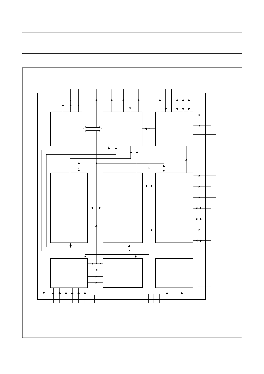
7
BLOCK DIAGRAM
handbook, full pagewidth
FEIN
(MUXC)
XTALO
XTALI
RESET
Y7 to Y0
SCL
SDA
SA
GPSW
(VBLK)
AP
SP
HS
RTCO
HSY
HCL
VS
SAA7110
SAA7110A
Y
Y
AD2 AD3
ANALOG
CONTROL
TEST
CONTROL
BLOCK
ANALOG
PROCESSING
CON
BYPASS
41
38
37
36
30
66
65
42
63
64
8
6
5
4
31
29
32
LLC2
CREF
UV7
to
UV0
i.c.
7, 8, 9
AI42
AI41
AI32
AI31
AI22
AI21
11
13
15
17
19
21
39
MGC820
40
ODD (VL)
PLIN (HL)
CGCE
LFCO
LLC
V
SSA0
V
DDA0
25
24
68, 52, 44,
34, 27
67, 51, 43,
35, 28
VSSA2 to VSSA4
VDDA2 to VDDA4
VSS
VDD
V
SS(S)
18, 14, 10
20, 16, 12
22
Y/CVBS
C/CVBS
1
2
3
26
33
AOUT
23
HREF
CHROMINANCE
CIRCUIT
LUMINANCE
CIRCUIT
SYNCHRONIZATION
CIRCUIT
CLOCK
GENERATION
CIRCUIT
BRIGHTNESS
CONTRAST
SATURATION
CONTROL
AND
OUTPUT
FORMATTER
POWER-ON
CONTROL
UV
Y
55 to 62
45 to 50,
53, 54
I
2
C-BUS
INTERFACE
I
2
C-BUS
CONTROL
CLOCKS
Fig.2 Block diagram.

1995 Oct 18
6
Philips Semiconductors
Product specification
One Chip Front-end 1 (OCF1)
SAA7110; SAA7110A
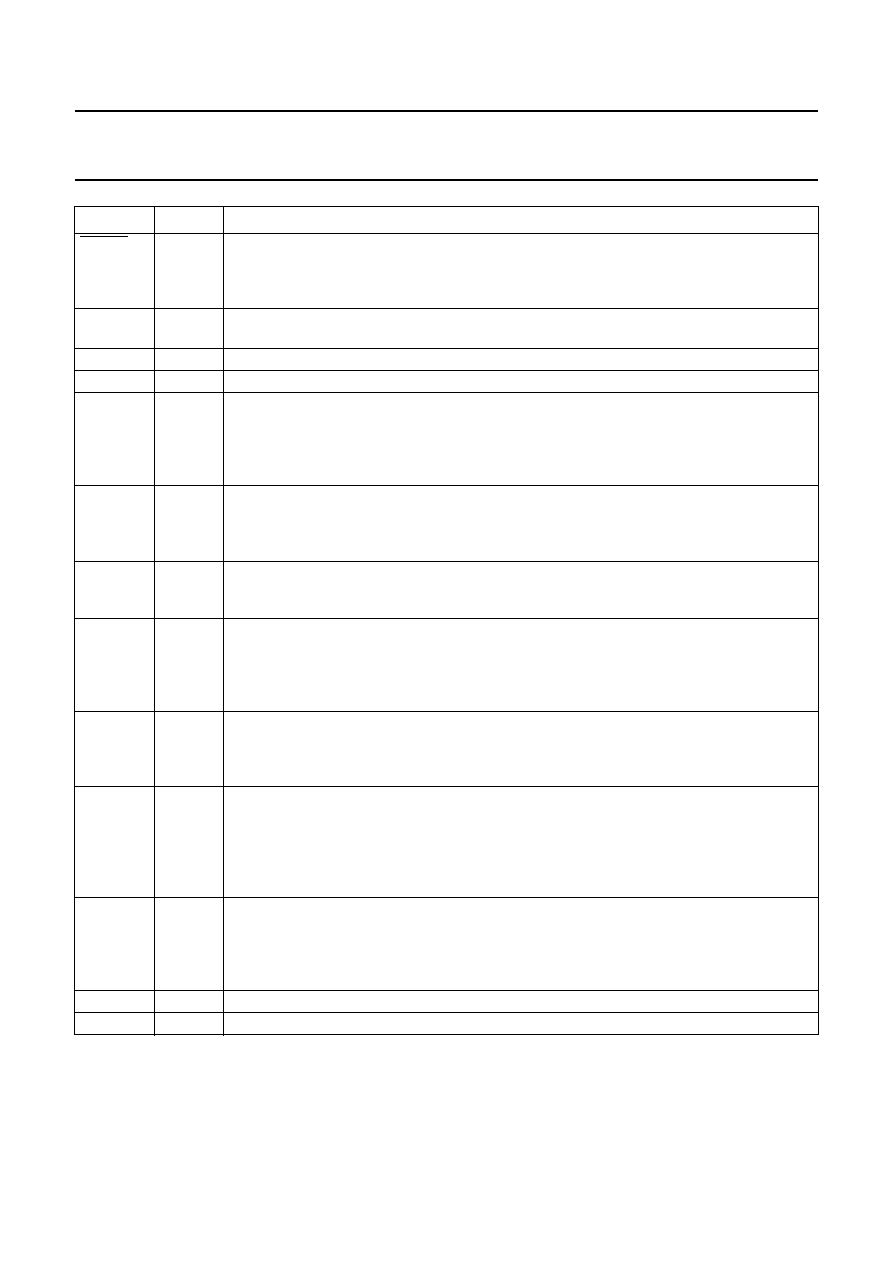
8
PINNING
SYMBOL
PIN
DESCRIPTION
SP
1
test pin input; (shift pin) connect to ground for normal operation
AP
2
test pin input; (action pin) connect to ground for normal operation
RTCO
3
Real Time Control Output. This pin is used to fit serially the increments of the HPLL and
FSC-PLL and information of the PAL or SECAM sequence.
SA
4
I
2
C-bus slave address select input. LOW: slave address = 9CH for write, 9DH for read;
HIGH = 9DH for write, 9FH for read.
SDA
5
I
2
C-bus serial data input/output
SCL
6
I
2
C-bus serial clock input
i.c.
7
reserved pin; do not connect
i.c.
8
reserved pin; do not connect
i.c.
9
reserved pin; do not connect
V
SSA4
10
ground for analog input 4
AI42
11
analog input 42
V
DDA4
12
supply voltage (+5 V) for analog input 4
AI41
13
analog input 41
V
SSA3
14
ground for analog input 3
AI32
15
analog input 32
V
DDA3
16
supply voltage (+5 V) for analog input 3
AI31
17
analog input 31
V
SSA2
18
ground for analog input 2
AI22
19
analog input 22
V
DDA2
20
supply voltage (+5 V) for analog input 2
AI21
21
analog input 21
V
SS(S)
22
substrate ground
AOUT
23
analog test output; do not connect
V
DDA0
24
supply voltage (+5 V) for internal CGC (Clock Generation Circuit)
V
SSA0
25
ground for internal CGC
LFCO
26
Line Frequency Control output; this is the analog clock control signal driving the external
CGC. The frequency is a multiple of the actual line frequency (nominally 7.375/6.13636 MHz).
The signal has a triangular form with 4-bit accuracy.
V
DD
27
supply voltage (+5 V)
V
SS
28
ground
LLC
29
Line-Locked Clock input/output (CGCE = 1, output; CGCE = 0, input). This is the system
clock, its frequency is 1888
◊
f
h
for 50 Hz/625 lines per field systems and 1560
◊
f
h
for
60 Hz/525 lines per field systems; or variable input clock up to 32 MHz in input mode.
LLC2
30
Line-Locked Clock
1
/
2
output; f
LLC2
= 0.5
◊
f
LLC
(CGCE = 1, output; CGCE = 0, high
impedance).
CREF
31
Clock reference input/output (CGCE = 1, output; CGCE = 0, input). This is a clock qualifier
signal distributed by the internal or an external clock generator circuit (CGC). Using CREF all
interfaces on the YUV-bus are able to generate a bus timing with identical phase.
1995 Oct 18
7
Philips Semiconductors
Product specification
One Chip Front-end 1 (OCF1)
SAA7110; SAA7110A
RESET
32
Reset active LOW input/output (CGCE = 1, output; CGCE = 0, input); sets the device into a
defined state. All data outputs are in high impedance state. The I
2
C-bus is reset (waiting for
START condition). Using the external CGC, the LOW period must be maintained for at least
30 LLC clock cycles.
CGCE
33
CGC Enable active HIGH input (CGCE = 1, on-chip CGC active; CGCE = 0, external CGC
mode, use SAA7197).
V
DD
34
supply voltage (+5 V)
V
SS
35
ground
HCL
36
Horizontal Clamping input/output pulse (programmable via I
2
C-bus bit PULIO: PULIO = 1,
output; PULIO = 0, input). This signal is used to indicate the black level clamping period for
the analog input interface. The beginning and end of its HIGH period (only in the output mode)
can be programmed via the I
2
C-bus registers 03H, 04H in 50 Hz mode and registers 16H,
17H in 60 Hz mode, active HIGH.
HSY
37
Horizontal Synchronization input/output indicator (programmable via I
2
C-bus bit PULIO:
PULIO = 1, output; PULIO = 0, input). This signal is fed to the analog interface. The beginning
and end of its HIGH period (only in the output mode) can be programmed via the I
2
C-bus
registers 01H, 02H in 50 Hz mode and registers 14H, 15H in 60 Hz mode, active HIGH.
HS
38
Horizontal Synchronization output (programmable; the HIGH period is 128 LLC clock cycles).
The position of the positive slope is programmable in 8 LLC increments over a complete line
(64
µ
s) via the I
2
C-bus register 05H in 50 Hz mode or register 18H in 60 Hz mode.
PLIN (HL)
39
PAL Identifier Not output; marks for demodulated PAL signals the inverted line (PLIN = LOW)
and a non-inverted line (PLIN = HIGH) and for demodulated SECAM the DR line
(PLIN = LOW) and the DB line (PLIN = HIGH). Select PLIN function via I
2
C-bus bit RTSE = 0.
(H-PLL locked output; a HIGH state indicates that the internal PLL has locked. Select HL
function via I
2
C-bus bit RTSE = 1).
ODD (VL)
40
ODD/EVEN field identification output; a HIGH state indicates the odd field. Select ODD
function via I
2
C-bus bit RTSE = 0.
(Vertical Locked output; a HIGH state indicates that the internal Vertical Noise Limiter (VNL)
is in a locked state. Select VL function via I
2
C-bus bit RTSE = 1).
VS
41
Vertical Synchronization input/output (programmable via I
2
C-bus bit OEHV: OEHV = 1,
output; OEHV = 0, input). This signal indicates the vertical synchronization with respect to the
YUV output. The high period of this signal is approximately six lines if the VNL function is
active. The positive slope contains the phase information for a deflection controller, for
example the TDA9150. In input mode this signal is used to synchronize the vertical gain and
clamp blanking stage, active HIGH.
HREF
42
Horizontal Reference output; this signal is used to indicate data on the digital YUV-bus. The
positive slope marks the beginning of a new active line. The HIGH period of HREF is either
768 Y samples or 640 Y samples long depending on the detected field frequency
(50/60 Hz mode). HREF is used to synchronize data multiplexer/demultiplexers. HREF is also
present during the vertical blanking interval.
V
SS
43
ground
V
DD
44
supply voltage (+5 V)
SYMBOL
PIN
DESCRIPTION
1995 Oct 18
8
Philips Semiconductors
Product specification
One Chip Front-end 1 (OCF1)
SAA7110; SAA7110A
Y7
45
Upper 6 bits of the 8-bit luminance (Y) digital output. As part of the digital YUV-bus
(data rate LLC/2), or A/D2(3) output (data rate LLC/2) selectable via I
2
C-bus bit SQPB = 1.
Y6
46
Y5
47
Y4
48
Y3
49
Y2
50
V
SS
51
ground
V
DD
52
supply voltage (+5 V)
Y1
53
Lower 2 bits of the 8-bit luminance (Y) digital output. As part of the digital YUV-bus
(data rate LLC/2), or A/D2(3) output (data rate LLC/2) selectable via I
2
C-bus bit SQPB = 1.
Y0
54
UV7
55
8-bit digital UV (colour difference) output; multiplexed colour difference signal for U and V
component of demodulated CVBS or chrominance signal. The format and multiplexing
scheme can be selected via I
2
C-bus control. These signals are part of the digital YUV-bus
(data rate LLC/2), or A/D3(2) output (data rate LLC/2) selectable via I
2
C-bus bit SQPB = 1.
UV6
56
UV5
57
UV4
58
UV3
59
UV2
60
UV1
61
UV0
62
FEIN
(MUXC)
63
Fast Enable input (active LOW); this signal is used to control fast switching on the digital
YUV-bus. A high at this input forces the IC to set its Y and UV outputs to the high impedance
state. To use this function set I
2
C-bus bits MS24 and MS34 and MUYC to LOW.
(Multiplex Components input; control signal for the analog multiplexers for fast switching
between locked Y/C signals or locked CVBS signals. FEIN automatically fixed to LOW (digital
YUV-bus enabled), if one of the three MUXC functions are selected (MS24 or MS34 or
MUYC = HIGH).
GPSW
(VBLK)
64
General Purpose Switch output; the state of this signal is programmable via I
2
C-bus register
0Dh, bit 1. Select GPSW function via I
2
C-bus bit VBLKA = 0. (Vertical Blank test output; select
VBLK via I
2
C-bus bit VBLKA = 1).
XTALO
65
Crystal oscillator output (to 26.8 MHz crystal); not used if TTL clock is used.
XTALI
66
Crystal oscillator input (from 26.8 MHz crystal) or connection of external oscillator with TTL
compatible square wave clock signal.
V
SS
67
ground
V
DD
68
supply voltage (+5 V)
SYMBOL
PIN
DESCRIPTION
1995 Oct 18
9
Philips Semiconductors
Product specification
One Chip Front-end 1 (OCF1)
SAA7110; SAA7110A
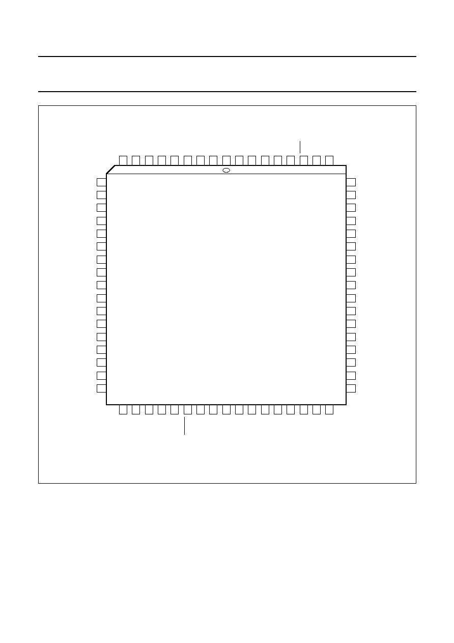
Fig.3 Pin configuration.
handbook, full pagewidth
SAA7110
SAA7110A
MGC822
10
11
12
13
14
15
16
17
18
19
20
21
22
23
24
25
26
60
59
58
57
56
55
54
53
52
51
50
49
48
47
46
45 Y7
Y6
Y5
Y4
Y3
Y2
Y1
Y0
UV7
UV6
UV5
UV4
UV3
UV2
44
27
28
29
LLC
LLC2
CREF
RESET
CGCE
HS
VS
PLIN (HL)
ODD (VL)
HREF
HCL
HSY
30
31
32
33
34
35
36
37
38
39
40
41
42
43
9
8
7
6
5
4
3
2
1
68
67
66
XTALI
XTALO
SP
AP
RTCO
SA
i.c.
i.c.
i.c.
SDA
SCL
GPSW (VBLK)
FEIN (MUXC)
UV0
UV1
65
64
63
62
61
VSSA4
AI42
VDDA4
AI41
AI32
AI31
AI22
AI21
AOUT
V
SSA3
V
DD
V
SS
V
DDA3
V
SSA2
V
DDA2
V
SS(S)
V
DDA0
V
DD
V
SS
V
DD
V
SS
V
SS
V
DD
V
SS
V
DD
V
SSA0
LFCO
1995 Oct 18
10
Philips Semiconductors
Product specification
One Chip Front-end 1 (OCF1)
SAA7110; SAA7110A
9
FUNCTIONAL DESCRIPTION
9.1
Analog input processing (see Fig.5)
The SAA7110; SAA7110A offers six analog signal inputs,
two analog main channels with clamping circuit, analog
amplifier, anti-alias filter and video CMOS ADC. A third
analog channel also with clamping circuit, analog amplifier
and anti-alias filter can be added or switched to both main
channels directly before the ADCs.
9.2
Analog control circuits
The clamping control circuit controls the correct clamping
of the analog input signals. The coupling capacitor is also
used to store and filter the clamping voltage. The normal
digital clamping level for luminance or CVBS signals is 64
and for chrominance signals is128.
The gain control circuits generate via I
2
C-bus the static
gain levels for the three analog amplifiers or controls one
of these amplifiers automatically via a built-in Automatic
Gain Control (AGC). The AGC is used to amplify a
CVBS or Y signal to the required signal amplitude,
matched to the ADCs input voltage range.
The anti-alias filters are adapted to the clock frequency.
The vertical blanking control circuit generates an I
2
C-bus
programmable vertical blanking pulse. During the vertical
blanking time gain and clamping control are frozen.
The fast switch control circuit is used for special
applications.
9.2.1
C
LAMPING
The coupling capacitor is used as clamp capacitance for
each input. An internal digital clamp comparator generates
the information concerning clamp-up or clamp-down. The
clamping levels for the two ADC channels are adjustable
over the 8-bit range (1 to 254). Clamping time in normal
use is set with the HCL pulse at the back porch of the video
signal. The clamping pulse HCL is user adjustable.
9.2.2
G
AIN CONTROL
(see Fig.4)
The luminance AGC can be used for every channel were
luminance or CVBS is being received. AGC active time is
the sync tip of the video signal. The sync tip pulse HSY is
user adjustable. The AGC can be switched off and the gain
for the three main input channels can be adjusted
independently. Signal (white) peak control limits the gain
at signal overshoots. The flow charts (see Figs 8 and 9)
show more details of the AGC. The influence of supply
voltage variation within the specified range is automatically
eliminated by clamp and automatic gain control.
9.3
Chrominance processing (see Fig.6)
The 8-bit chrominance signal passes the input interface,
the chrominance bandpass filter to eliminate DC
components, and is finally fed to the multiplication inputs
of a quadrature demodulator, where two subcarrier signals
from the local oscillator DTO1 with 90 degrees phase shift
are applied. The frequency is dependent on the present
colour standard.
The multiplier operates as a quadrature demodulator for all
PAL and NTSC signals; it operates as a frequency down
mixer for SECAM signals.
The two multiplier output signals are converted to a serial
UV data stream and applied to two low-pass filter stages,
then to a gain controlled amplifier. A final multiplexed
low-pass filter achieves, together with the preceding
stages, the required bandwidth performance.
The PAL and NTSC originated signals are applied to a
comb filter.
The signal originated from SECAM is fed through a Cloche
filter (0 Hz centre frequency), a phase demodulator and a
differentiator to obtain frequency demodulated colour
difference signals. The SECAM signal is fed after
de-emphasis to a cross-over switch, to provide both the
serial transmitted colour difference signals. These signals
are fed to the BCS control and finally to the output fomatter
stage and to the output interface.
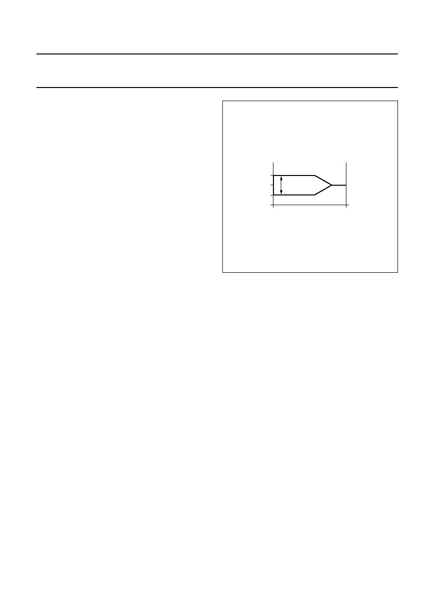
Fig.4 Automatic gain control range.
handbook, halfpage
analog input level
controlled
ADC input level
maximum
minimum
range 8.8 dB
0 dB
0 dB
MGC823
+
2.8 dB
-
6 dB

1995 Oct 18
11
Philips Semiconductors
Product specification
One Chip Front-end 1 (OCF1)
SAA7110; SAA7110A
9.4
Luminance processing (see Fig.7)
The 8-bit luminance signal, a digital CVBS format or a
luminance format (S-VHS, HI8), is fed through a
switchable prefilter. High frequency components are
emphasized to compensate for loss. The following
chrominance trap filter (f
c
= 4.43 or 3.58 MHz centre
frequency selectable) eliminates most of the colour carrier
signal, therefore, it must be bypassed for S-Video (S-VHS,
HI8) signals.
The high frequency components of the luminance signal
can be peaked (control for sharpness improvement via
I
2
C-bus) in two bandpass filters with selectable transfer
characteristics.
A coring circuit with selectable characteristics improves
the signal once more. This signal is then added to the
original (unpeaked) signal. A switchable amplifier achieves
common DC amplification, because the DC gains are
different in both chrominance trap modes.
The improved luminance signal is fed via the variable
delay to the BCS control and the output interface.
9.5
YUV-bus (digital outputs)
The 16-bit YUV-bus transfers digital data from the output
interfaces to a feature box, or a field memory, a digital
colour space converter (SAA 7192 DCSC) or a video
enhancement and digital-to-analog processor (SAA7165
VEDA2). The outputs are controlled by an output enable
chain (FEIN on pin 63).
The YUV data rate equals LLC2. Timing is achieved by
marking each second positive rising edge of the clock LLC
in conjunction with CREF (clock reference).
The output signals Y7 to Y0 are the bits of the digital
luminance signal. The output signals UV7 to UV0 are the
bits of multiplexed colour difference signals (B
-
Y) and
(R
-
Y). The frame in the format tables is the time, required
to transfer a full set of samples. In the event of 4 : 2 : 2
format two luminance samples are transmitted in
comparison to one U and one V sample within the frame.
The time frames are controlled by the HREF signal.
Fast enable is achieved by setting input FEIN to LOW. The
signal is used to control fast switching on the digital
YUV-bus. HIGH on this pin forces the Y and UV outputs to
a high-impedance state.
9.6
Synchronization (see Fig.7)
The pre-filtered luminance signal is fed to the
synchronization stage. It's bandwidth is reduced to 1 MHz
in a low-pass filter.
The synchronization pulses are sliced and fed to the phase
detectors where they are compared with the sub-divided
clock frequency. The resulting output signal is applied to
the loop filter to accumulate all phase deviations.
Adjustable output signals HCL and HSY are generated in
accordance with analog front end requirements. The
output signals HS, VS, and PLIN are locked to the timing
reference, guaranteed between the input signal and the
HREF signal, as further improvements to the circuit may
change the total processing delay. It is therefore not
recommended to use them for applications which require
absolute timing accuracy to the input signals. The loop
filter signal drives an oscillator to generate the line
frequency control signal LFCO.
9.7
Clock generation circuit
The internal CGC generates all clock signals required for
the one chip front-end. The output signal LFCO is a
digital-to-analog converted signal provided by the
horizontal PLL. It is the multiple of the line frequency
(7.38 MHz = 472
◊
f
h
in 50 Hz systems and
6.14 MHz = 360
◊
f
h
in 60 Hz systems). Internally the
LFCO signal is multiplied by a factor of 2 or 4 in the PLL
circuit (including phase detector, loop filtering, VCO and
frequency divider) to obtain the LLC and LLC2 output clock
signals. The rectangular output clocks have a 50% duty
factor.
It is also possible to operate the OCF1 with an external
CGC (SAA7197) providing the signals LLC and CREF.
The selection of the internal/external CGC will be
controlled by the CGCE input signal.
9.8
Power-on reset
Power-on reset is activated at power-on (using only
internal CGC), when the supply voltage decreases below
3.5 V. The indicator output RESET is LOW for a time. The
RESET signal can be applied to reset other circuits of the
digital TV system.
9.9
RTCO output
The real time control and status output signal contains
serial information about actual system clock, subcarrier
frequency and PAL/SECAM sequence. The signal can be
used for various applications in external circuits, for
example, in a digital encoder to achieve clean encoding.

1995
Oct
18
12
Philips Semiconductors
Product specification
One Chip Front-end 1 (OCF1)
SAA71
10; SAA71
10A
This text is here in white to force landscape pages to be rotated correctly when browsing through the pdf in the Acrobat reader.This text is here in
_
white to force landscape pages to be rotated correctly when browsing through the pdf in the Acrobat reader.This text is here inThis text is here in
white to force landscape pages to be rotated correctly when browsing through the pdf in the Acrobat reader. white to force landscape pages to be ...
handbook, full pagewidth
ANALOG
CONTROL
MGC824
SOURCE
SWITCH
CLAMP
CIRCUIT
ANALOG
AMPLIFIER
ANALOG
AMPLIFIER
ANALOG
AMPLIFIER
GAIN
CONTROL
CLAMP
CONTROL
CROSS
MULTIPLEXER
ANTI-ALIAS
FILTER
BYPASS
SWITCH
SOURCE
SWITCH
CLAMP
CIRCUIT
ANTI-ALIAS
FILTER
BYPASS
SWITCH
FAST
SWITCH
ADDER
FAST
SWITCH
ADDER
FAST
SWITCH
CONTROL
VERTICAL
BLANKING
CONTROL
SOURCE
SWITCH
CLAMP
CIRCUIT
ANTI-ALIAS
FILTER
ANTI-ALIAS
CONTROL
BYPASS
SWITCH
TEST
SELECTOR
FUSE
FUSE
FUSE
REFS4
AINS4
AIND4
REFS3
REFS2
AINS3
AIND3
AINS2
AIND2
CLTS
CLS2
CLS3
CLS4
AOSL
ADC
ADC
YSEL
CSEL
TWO2
TWO3
VDDA2 to VDDA4
VSSA2 to VSSA4
AI42
AI41
AI32
AI31
AI22
AI21
i.c.
i.c.
i.c.
VSS(S)
11
20, 16, 12
18, 14, 10
13
15
17
19
21
9
8
7
22
CLL2n
CLL3n
WIPA
GLIM
HOLD
WIPE
SBOT
GASL
GACO
GAI2
GAI3
GAI4
IWIP
IGAI
VBPS
VBPR
VBCO
MUYC
MS24
MS34
MX24
MX34
MUD1
MUD2
WISL
IVAL
WVAL
GUDL
WIRS
GAS2
GAS3
GAD2
GAD3
WRSE
23
AOUT
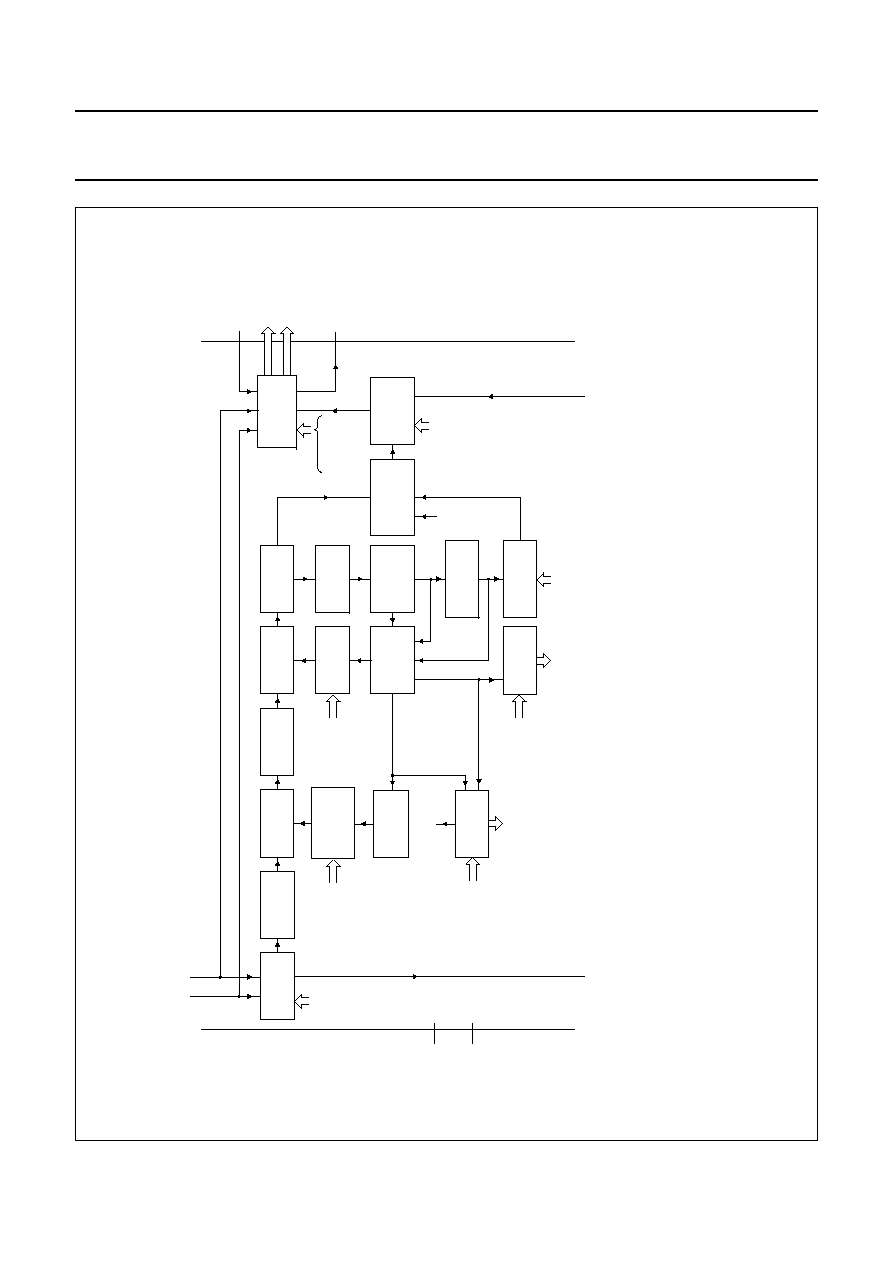
Fig.5 Analog input processing and analog control part.
1995
Oct
18
13
Philips Semiconductors
Product specification
One Chip Front-end 1 (OCF1)
SAA71
10; SAA71
10A
This text is here in white to force landscape pages to be rotated correctly when browsing through the pdf in the Acrobat reader.This text is here in
_
white to force landscape pages to be rotated correctly when browsing through the pdf in the Acrobat reader.This text is here inThis text is here in
white to force landscape pages to be rotated correctly when browsing through the pdf in the Acrobat reader. white to force landscape pages to be ...
handbook, full pagewidth
INPUT
INTERFACE
CHROMINANCE
BANDPASS
OUTPUT
FORMATTER
AND INTERFACE
QUADRATURE
DEMODULATOR
LOW-PASS
LOW-PASS
GAIN
CONTROL
CLOCH FILTER
LOOPFILTER
PI2
LOOP FILTER
PI1
SEQUENCE
PROCESSOR
PHASE
DEMODULATOR
AMPLITUDE
DETECTOR
BRIGHTNESS
CONTRAST
SATURATION
CONTROL
COMB FILTERS
AND SECAM
RECOMBINATION
BURST GATE
ACCUMULATOR
DISCRETE TIME
OSCILLATOR
(DTO1)
AND DIVIDER
STANDARD
CONTROL
BRIG
CONT
SATN
DIFFERENTIATOR
DE-EMPHASIS
SXCR
CODE
BYPS
CHRS
COLO
SECS
CHCV
CKTQ
CKTS
LFIS
SEQA
SESE
PLSE
ALTD
VDD
VSS
CHROMINANCE CIRCUIT
68, 52, 44,
34, 27
67, 51, 43,
35, 28
63
42
OFTS
CHSB
OEYC
OEHV
SQPB
HRMV
HRFS
SEQA
HUEC
FEIN
(MUXC)
HREF
UV7 to UV0
Y7 to Y0
45 to 50,
53, 54
MGC825
55 to
62
Fig.6 Multi-standard decoder part.
1995
Oct
18
14
Philips Semiconductors
Product specification
One Chip Front-end 1 (OCF1)
SAA71
10; SAA71
10A
This text is here in white to force landscape pages to be rotated correctly when browsing through the pdf in the Acrobat reader.This text is here in
_
white to force landscape pages to be rotated correctly when browsing through the pdf in the Acrobat reader.This text is here inThis text is here in
white to force landscape pages to be rotated correctly when browsing through the pdf in the Acrobat reader. white to force landscape pages to be ...
handbook, full pagewidth
PREFILTER
PREFILTER
SYNC
I
2
C-BUS
INTERFACE
I
2
C-BUS
CONTROL
SYNC
SLICER
TEST
CONTROL
BLOCK
CHROMINANCE
TRAP
PHASE
DETECTOR
FINE
PHASE
DETECTOR
COARSE
LOOP FILTER
2
DELAY
ADJUSTMENT
LINE-LOCKED
CLOCK
GENERATOR
DISCRETE TIME
OSCILLATOR
(DTO2)
CRYSTAL
CLOCK
GENERATOR
VARIABLE
BANDPASS
FILTER
CORING
WEIGHTING
AND
ADDING STAGE
VARIABLE
DELAY
POWER-ON
CONTROL
PREF
BYPS
CORI
APER
YDEL
CLOCK(3 to 0)
BFBY
PREF
BPSS
MATCHING
AMPLIFIER
DAC6
CLOCK
GENERATION
CIRCUIT
DAC4
COUNTER
VERTICAL
PROCESSOR
FIDT
HLCK
STTC
VBLKA
SSTB
GPSW
VNOI
FSEI
AUFD
HS6B
HS6S
HC6B
HC6S
PULIO
OEHV
SCEN
IDEL
HSYB
HSYS
HCLB
HCLS
HPHI
HP6I
SYNCHRONIZATION CIRCUIT
LUMINANCE CIRCUIT
HLCK
VTRC
HPLL
HLCK
AP
SP
SA
SCL SDA
36
64
4
5
6
41
37 38 39
40
25
24
33
3
HCL
HS
VS
CGCE
ODD (VL)
VSSA0
VDDA0
RTCO
HSY
PLIN (HL)
26
65
66
30
29
31
32
RESET
CREF
LLC
LLC2
XTALI
XTALO
LFCO
GPSW
(VBLK)
2
1
MGC826
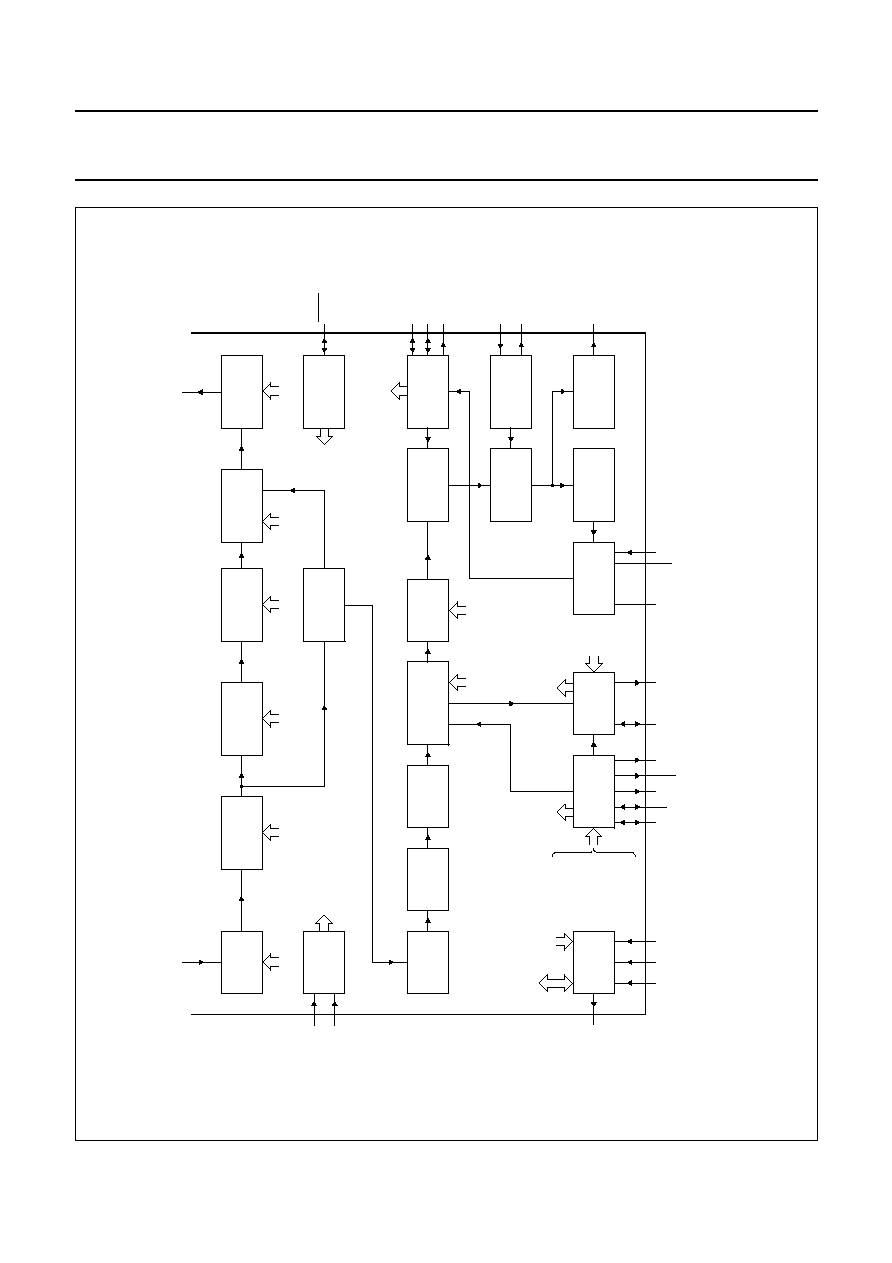
Fig.7 Luminance and synchronization part.

1995 Oct 18
15
Philips Semiconductors
Product specification
One Chip Front-end 1 (OCF1)
SAA7110; SAA7110A
10 GAIN CHARTS
Fig.8 Clamp and gain flow chart.
CLAU = clamp up.
VBLK = vertical blanking pulse.
WIPE = white peak level (adjustable).
SBOT = sync bottom level (adjustable).
CLL = clamp level (adjustable).
CLAA = clamp active.
HSY = horizontal sync pulse.
HCL = horizontal clamp pulse.
handbook, full pagewidth
ADC
ANALOG IN
VBLK
NO BLANKING ACTIVE
CLAA
=
1
HCL
<CCL
HSY
>
SBOT
>
WIPE
CLAA
=
0
CLAU
=
1
CLAU
=
0
1
0
1
0
MGC827
+
CLAMP
-
CLAMP
+
GAIN
-
GAIN
-
GAIN
SLOW
+
GAIN
NO
CLAMP
1
0
1
0
1
0
1
0
<-
CLAMP
GAIN
->

1995 Oct 18
16
Philips Semiconductors
Product specification
One Chip Front-end 1 (OCF1)
SAA7110; SAA7110A
handbook, full pagewidth
analog input
amplifier
anti-alias amplifier
ADC8
decoder input
X
HSY
WRSE
>
WIPE
>
WIPE
<
SBOT
<
SBOT
WIRS
X
=
1
X
=
0
-
IVAL
+
IVAL
-
WVAL
+
/
-
0
+
4/F
+
4/L
gain accumulator (20 bits)
actual gain value 8-bit (AGV) [
-
3/
+
6 dB]
X
STOP
HSY
Y
update
FGV
MGC828
AGV
gain value 8-bit
1
0
1
0
1
0
1
0
1
0
1
0
1
0
0
1
1
0
1
0
1
0
VBLK
1
0
no action
MSB
6
LSB
2
*IWIP
*IGAI
*IWIP
Fig.9 Luminance AGC flow chart.
X = system variable (start with logic 0).
Y = IAGV-FGVI > GUDL.
VBLK = vertical blanking pulse.
HSY = horizontal sync pulse.
SBOT = sync bottom level (adjustable).
WIPE = white peak level (adjustable).
IVAL = integration value gain (adjustable).
WVAL = integration value WIPE (adjustable).
IGAI = integration factor gain (adjustable).
IWIP = integration factor WIPE (adjustable).
AGV = actual gain value.
FGV = frozen gain value.
GUDL = gain update level (adjustable).
WRSE = white peak reset enable.
WIRS = white peak reset select.
L = line.
F = field.

1995 Oct 18
17
Philips Semiconductors
Product specification
One Chip Front-end 1 (OCF1)
SAA7110; SAA7110A
11 LIMITING VALUES
In accordance with the Absolute Maximum Rating System (IEC 134); all ground pins and all supply pins connected
together.
Note
1. Compare with typical total power consumption in Chapter "Characteristics".
2. Equivalent to discharging a 100 pF capacitor through a 1.5 k
series resistor.
12 CHARACTERISTICS
V
DDD
= 5 V; V
DDA
= 5 V; T
amb
= 25
∞
C; unless otherwise specified.
SYMBOL
PARAMETER
CONDITIONS
MIN.
MAX.
UNIT
V
DDA
analog supply voltage
-
0.5
+7.0
V
V
DDD
digital supply voltage
-
0.5
+7.0
V
V
I(A)
analog input voltage
-
0.5
+7.0
V
V
I(D)
digital input voltage
-
0.5
+7.0
V
V
diff
voltage difference between V
SSAall
and V
SSall
-
100
mV
T
stg
storage temperature
-
65
+150
∞
C
T
amb
operating ambient temperature
0
70
∞
C
T
amb(bias)
operating ambient temperature under bias
-
10
+80
∞
C
P
tot
total power dissipation
V
DDA
= V
DDD
= 7 V; note 1
-
2.5
W
V
esd
electrostatic discharge all pins
note 2
-
2000
+2000
V
SYMBOL
PARAMETER
CONDITIONS
MIN.
TYP.
MAX.
UNIT
Supplies
V
DDA
analog supply voltage
4.75
5.0
5.25
V
V
DDD
digital supply voltage
4.5
5.0
5.5
V
I
DDA(tot)
total analog supply current
-
-
150
mA
I
DDD(tot)
total digital supply current
-
-
250
mA
P
tot
total power dissipation
-
1.2
1.7
W
Analog part
I
clamp
clamping current
V
I
= 1.25 V DC
-
2
-
+2
µ
A
V
i(p-p)
input voltage (peak-to-peak
value), AC coupling required
C
couple
= 10 nF
0.5
1.0
1.38
V
Z
i
input impedance
clamping current off
200
-
-
k
C
i
input capacitance
-
-
10
pF
ct
channel crosstalk
f
i
< 5 MHz
-
-
50
-
dB
Analog-to-digital converters
B
analog bandwidth
at
-
3 dB
-
15
-
MHz
diff
differential phase
amplifier + AAF = bypass
-
2
-
deg
G
diff
differential gain
amplifier + AAF = bypass
-
2
-
%
f
LLC
ADC clock rate
11
-
16
MHz
DLE
DC differential linearity error
-
1
/
2
-
LSB
ILE
DC integral linearity error
-
1
-
LSB
1995 Oct 18
18
Philips Semiconductors
Product specification
One Chip Front-end 1 (OCF1)
SAA7110; SAA7110A
Digital inputs
V
IL
LOW level input voltage
SDA and SCL
-
0.5
-
+1.5
V
V
IH
HIGH level input voltage
SDA and SCL
3.0
-
V
DD
+ 0.5
V
V
IL(clk)
LOW level input voltage for
clocks
-
0.5
-
+0.6
V
V
IH(clk)
HIGH level input voltage for
clocks
2.4
-
V
DD
+ 0.5
V
V
IH(XTALI)
HIGH level input voltage XTALI
3.0
-
V
DD
+ 0.5
V
V
IL(n)
LOW level input voltage all other
inputs
-
0.5
-
+0.8
V
V
IH(n)
HIGH level input voltage all other
inputs
2.0
-
V
DD
+ 0.5
V
I
LI
input leakage current
-
-
10
µ
A
C
i(clk)
input capacitance for clocks
-
-
10
pF
C
i(I/O)
input capacitance
I/Os at high impedance
-
-
8
pF
C
i(n)
input capacitance all other inputs
-
-
8
pF
Digital outputs
V
LFCO
LFCO output voltage
(peak-to-peak value)
note 1
1.4
-
2.6
V
V
OL
LOW level output voltage
note 2
0
-
0.6
V
V
OH
HIGH level output voltage
note 2
2.4
-
V
DD
V
V
OL(clk)
LOW level output voltage for
clocks
-
0.5
-
+0.6
V
V
OH(clk)
HIGH level output voltage for
clocks
2.6
-
V
DD
+ 0.5
V
Clock input timing (LLC)
T
cy
cycle time
31
-
45
ns
duty factor for t
LLCH
/T
cy
40
-
60
%
t
r
rise time
V
i
= 0.6 to 2.4 V
-
-
5
ns
t
f
fall time
V
i
= 2.4 to 0.6 V
-
-
5
ns
Control and CREF input timing (note 3)
t
SU;DAT
input data set-up time
11
-
-
ns
t
HD;DAT
input data hold time
3
-
-
ns
t
HD;FEIN
input data hold time for FEIN
3
-
-
ns
t
HD;OTHER
input data hold time all other
inputs
note 3
6
-
-
ns
SYMBOL
PARAMETER
CONDITIONS
MIN.
TYP.
MAX.
UNIT
1995 Oct 18
19
Philips Semiconductors
Product specification
One Chip Front-end 1 (OCF1)
SAA7110; SAA7110A
Data and control output timing (note 4)
C
L(data)
output load capacitance
(data, HREF and VS)
15
-
50
pF
C
L(control)
output load capacitance (control)
7.5
-
25
pF
t
HD;DAT
output data hold time
C
L
= 15 pF
13
-
-
ns
t
PD(data)
propagation delay from negative
edge of LLC (data, HREF and
VS)
C
L
= 50 pF
-
-
29
ns
t
PD(control)
propagation delay from negative
edge of LLC (control)
C
L
= 25 pF
-
-
29
ns
t
PD(Z))
propagation delay from negative
edge of LLC (to 3-state)
note 5
-
-
15
ns
Clock output timing (LLC and LLC2)
C
L(LLC)
output load capacitance
15
-
40
pF
T
cy
cycle time
LLC
31.5
-
45
ns
LLC2
63
-
90
ns
duty factors for t
LLCH
/t
LLC
and
t
LLC2H
/t
LLC2
40
-
60
%
t
r
rise time
0.6 to 2.6 V
-
-
5
ns
t
f
fall time
2.6 to 0.6 V
-
-
5
ns
t
d
delay time LLC output to LLC2
output
V
i
= 1.5 V;
C
LLC/LLC2
= 40 pF; note 6
-
-
8
ns
Data qualifier output timing (CREF)
t
HD;CREF
output hold time
C
L
= 15 pF
4
-
-
ns
t
PD;CREF
propagation delay from positive
edge of LLC
C
L
= 40 pF
-
-
20
ns
Horizontal PLL
f
Hnom
nominal line frequency
50 Hz field
-
15625
-
Hz
60 Hz field
-
15734
-
Hz
f
H
/f
Hnom
permissible static deviation
50 Hz field
-
-
5.6
%
60 Hz field
-
-
6.7
%
Subcarrier PLL
f
Hnom
nominal subcarrier frequency
PAL
-
4433618
-
Hz
NTSC
-
3579545
-
Hz
f
H
/f
Hnom
lock-in range
400
-
-
Hz
SYMBOL
PARAMETER
CONDITIONS
MIN.
TYP.
MAX.
UNIT

1995 Oct 18
20
Philips Semiconductors
Product specification
One Chip Front-end 1 (OCF1)
SAA7110; SAA7110A
Notes
1. The LFCO output level must be measured with a load circuit of 10 k
in parallel with 15 pF.
2. The levels must be measured with load circuits, the loads depend on the type of output stage. Control outputs (except
HREF and VS); 1.2 k
at 3 V (TTL load); C
L
= 25 pF: data outputs (plus HREF and VS); 1.2 k
at 3 V (TTL load);
C
L
= 50 pF.
3. Other control input signals are CGCE, VS, SA, HCL and HSY.
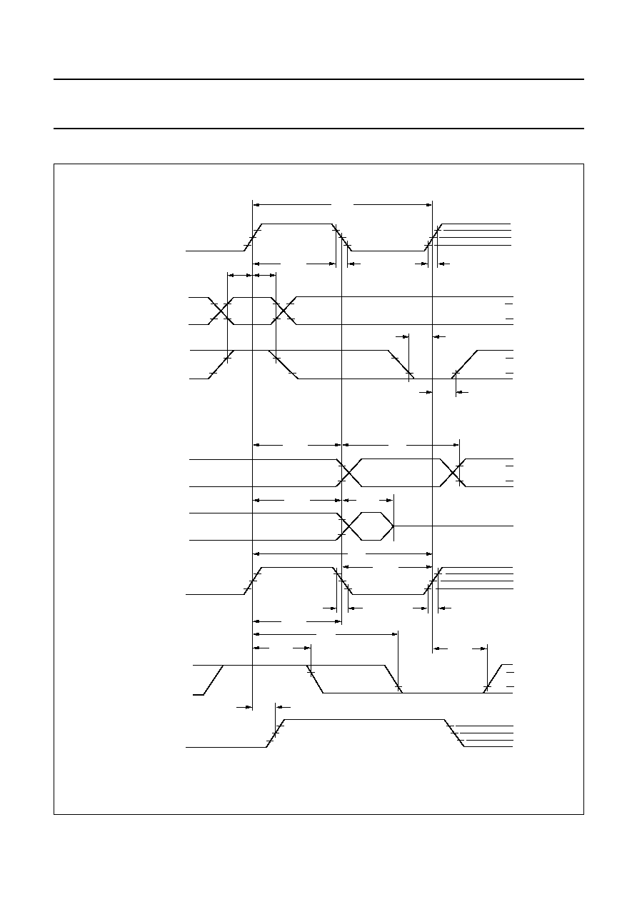
4. Data output signals are YUV (15 to 0). Control output signals are HREF, VS, HS, HSY, HCL, RTCO, PLIN (HL),
ODD (VL) and GPSW0 (VBLK). The effects of rise and fall times are included in the calculation of t
HD;DAT
, t
PD
and
t
PDZ
. Timings and levels refer to drawings and conditions illustrated in Fig.10.
5. The minimum propagation delay from 3-state to data active related to falling edge of LLC is 0 ns.
6. LLC2 is not active while CGCE = 0.
7. Philips catalogue number 9922 520 30004.
Table 1
Processing delay
Crystal oscillator
f
n
nominal frequency
3rd harmonic
-
26.8
-
MHz
f/f
n
permissible frequency deviation
-
50
◊
10
-
6
-
+50
◊
10
-
6
T/f
n
permissible frequency deviation
with temperature
-
20
◊
10
-
6
-
+20
◊
10
-
6
C
RYSTAL SPECIFICATION
(X1); note 7
T
amb
operating ambient temperature
0
-
70
∞
C
C
L
load capacitance
8
-
-
pF
R
s
series resonance resistance
-
50
80
C1
motional capacitance
-
1.1
±
20%
-
fF
C0
parallel capacitance
-
3.5
±
20%
-
pF
FUNCTION
TYPICAL ANALOG DELAY
AI21 TO ADCIN (AOUT) (ns)
DIGITAL DELAY
ADCIN (AOUT) TO YUVOUT
(1/LLC)
(YDEL = 0; CAD2/3 = 1)
Without amplifier or anti-alias filter
10
248
With amplifier, without anti-alias filter
30
With amplifier plus anti-alias filter (50 Hz)
30 + 40
With amplifier plus anti-alias filter (60 Hz)
30 + 50
SYMBOL
PARAMETER
CONDITIONS
MIN.
TYP.
MAX.
UNIT
1995 Oct 18
21
Philips Semiconductors
Product specification
One Chip Front-end 1 (OCF1)
SAA7110; SAA7110A
13 TIMING
Fig.10 Clock/data timing.
handbook, full pagewidth
,,,
,,,
,,,,,,,,,
,,,,,,,,,
,,,
,,,
,,,,,
,,,,,
,,,
,,,
,,,
,,,
,,,,,,,
,,,,,,,
,,,
,,,
,,,,
,,,,
,,
,,
Tcy
Tcy
tf
tSU;DAT
tr
tLLCH
tSU;DAT
tHD;DAT
tHD;DAT
tHD;DAT
tOHD
tOHD
tPD
tPDZ
tPD
tOHD
tOHD
tLLCL
tLLCH
tf
tdLLC2
tr
CLOCK INPUT LLC
INPUTS CONTROL
INPUT CREF
OUTPUTS YUV, HREF, VS AND HS
OUTPUTS YUV (to 3-state)
CLOCK OUTPUT LLC
OUTPUT CREF
CLOCK OUTPUT LLC2
2.4 V
1.5 V
0.6 V
2.6 V
1.5 V
0.6 V
2.6 V
1.5 V
0.6 V
2.0 V
0.8 V
2.0 V
0.8 V
2.4 V
0.6 V
2.4 V
0.6 V
MGC829
1995 Oct 18
22
Philips Semiconductors
Product specification
One Chip Front-end 1 (OCF1)
SAA7110; SAA7110A
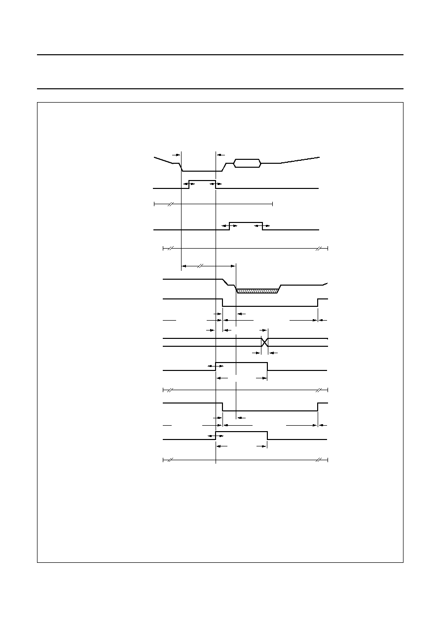
Fig.11 Horizontal timing.
(1) See Table 1.
HRMV = 1 and HRFS = 0.
handbook, full pagewidth
0
+
117
-
118
+
97
-
97
MGC830
CVBS
HSY
HCL
62
◊
2/LLC
30
◊
2/LLC
Y output
HREF (50 Hz)
18
◊
2/LLC
768
◊
2/LLC
176
◊
2/LLC
18
◊
2/LLC
140
◊
2/LLC
640
◊
2/LLC
64
◊
2/LLC
burst
PLIN (50 Hz)
processing delay CVBS
->
YUV
0
+
191
-
64
0
4/LLC
HREF (60 Hz)
HS (60 Hz)
HS (50 Hz)
programming range
(step size: 8/LLC)
+
127
-
128
HCL
programming range
(step size: 2/LLC)
HSY
programming range
(step size: 2/LLC)
HS (60 Hz)
programming range
(step size: 8/LLC)
HS (50 Hz)
94
◊
2/LLC
64
◊
2/LLC
(1)
1995 Oct 18
23
Philips Semiconductors
Product specification
One Chip Front-end 1 (OCF1)
SAA7110; SAA7110A
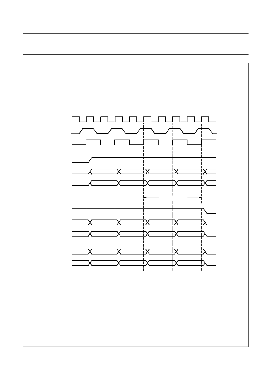
Fig.12 HREF timing.
handbook, full pagewidth
0
1
2
3
4
U0
V0
U1
V1
U2
END OF ACTIVE LINE
START OF ACTIVE LINE
767
766
765
764
763
U766
V766
V764
U764
V762
639
638
637
636
635
U638
V638
MGC831
V636
U636
V634
ONE BUS CYCLE
LL27
CREF
HREF
Yn
Yn
(50 Hz)
UVn
Yn
(60 Hz)
UVn
UVn
HREF
INTERNAL
BUS CLOCK

1995 Oct 18
24
Philips Semiconductors
Product specification
One Chip Front-end 1 (OCF1)
SAA7110; SAA7110A
Fig.13 Vertical timing.
(1) Nominal input signal 50 Hz.
(2) Nominal input signal 60 Hz.
HRMV = 1 and HRFS = 0.
handbook, full pagewidth
1
2
3
4
5
6
7
8
9
625
input CVBS
HREF
a: 1st field
(1)
2
◊
2/LLC
533
◊
2/LLC
ODD
VS
314
315
316
317
318
319
320
321
313
input CVBS
HREF
b: 2nd field
(1)
2
◊
2/LLC
61
◊
2/LLC
ODD
VS
1
2
3
4
5
6
7
8
9
525
input CVBS
HREF
a: 1st field
(2)
2
◊
2/LLC
441
◊
2/LLC
ODD
VS
264
265
266
267
268
269
270
271
263
input CVBS
HREF
b: 2nd field
(2)
2
◊
2/LLC
51
◊
2/LLC
ODD
VS
MGC832

1995 Oct 18
25
Philips Semiconductors
Product specification
One Chip Front-end 1 (OCF1)
SAA7110; SAA7110A
Fig.14 FEIN timing.
handbook, full pagewidth
LLC
CREF
HREF
FEIN
YUV
t
SU;DAT
t
HD;DAT
MGC833
t
OHD
tPD
from 3-state
to 3-state
Table 2
Digital output control
OEYC
FEIN
YUV (15 : 0)
0
0
Z
1
0
active
X
1
Z
Fig.15 Real time control output timing.
RTCO sequence is generated in LLC/4.
For transmission LLC/2 timing is required.
handbook, full pagewidth
TIME SLOT:
BIT NO.:
transmitted once per line
22
1
21
19
20
15
16
17
18
7
8
9
11 10
12
13
14
SEQUENCE
19
0
67
4
3
6
4
5
2
3
0
14
45
RESERVED
14
FSCPLL-INCR.
MGC834
276
63
0
1
RESERVED
128
HIGH
LOW
13
HPLL-INCR.
RESERVED
1
(50 Hz SYSTEMS)
188
(60 Hz SYSTEMS)
1995 Oct 18
26
Philips Semiconductors
Product specification
One Chip Front-end 1 (OCF1)
SAA7110; SAA7110A
14 OUTPUT FORMATS
Table 3
Output formats
BUS
SIGNAL
PIXEL BYTE SEQUENCE 4 : 1 : 1 FORMAT
PIXEL BYTE SEQUENCE 4 : 2 : 2 FORMAT
Y7
Y7
Y7
Y7
Y7
Y7
Y7
Y7
Y7
Y7
Y7
Y7
Y7
Y7
Y7
Y6
Y6
Y7
Y6
Y6
Y6
Y6
Y6
Y6
Y6
Y6
Y6
Y6
Y6
Y6
Y5
Y5
Y5
Y5
Y5
Y5
Y5
Y5
Y5
Y5
Y5
Y5
Y5
Y5
Y5
Y4
Y4
Y4
Y4
Y4
Y4
Y4
Y4
Y4
Y4
Y4
Y4
Y4
Y4
Y4
Y3
Y3
Y3
Y3
Y3
Y3
Y3
Y3
Y3
Y3
Y3
Y3
Y3
Y3
Y3
Y2
Y2
Y2
Y2
Y2
Y2
Y2
Y2
Y2
Y2
Y2
Y2
Y2
Y2
Y2
Y1
Y1
Y1
Y1
Y1
Y1
Y1
Y1
Y1
Y1
Y1
Y1
Y1
Y1
Y1
Y0
Y0
Y0
Y0
Y0
Y0
Y0
Y0
Y0
Y0
Y0
Y0
Y0
Y0
Y0
UV7
U7
U5
U3
U1
U7
U5
U3
U1
U7
V7
U7
V7
U7
V7
UV6
U6
U4
U2
U0
U6
U4
U2
U0
U6
V6
U6
V6
U6
V6
UV5
V7
V5
V3
V1
V7
V5
V3
V1
U5
V5
U5
V5
U5
V5
UV4
V6
V4
V2
V0
V6
V4
V2
V0
U4
V4
U4
V4
U4
V4
UV3
0
0
0
0
0
0
0
0
U3
V3
U3
V3
U3
V3
UV2
0
0
0
0
0
0
0
0
U2
V2
U2
V2
U2
V2
UV1
0
0
0
0
0
0
0
0
U1
V1
U1
V1
U1
V1
UV0
0
0
0
0
0
0
0
0
U0
V0
U0
V0
U0
V0
Y frame
0
1
2
3
4
5
6
7
0
1
2
3
4
5
UV frame
0
4
0
2
4
data rate
sample frequency
data rate
sample frequency
Y
LLC2
LLC2
LLC2
LLC2
U
LLC4
LLC8
V
LLC4
LLC8
1995 Oct 18
27
Philips Semiconductors
Product specification
One Chip Front-end 1 (OCF1)
SAA7110; SAA7110A
Fig.16 YUV output signal range.
CCIR 601 digital levels.
handbook, full pagewidth
LUMINANCE 100%
+
255
+
235
+
128
+
16
0
U-COMPONENT
+
255
+
240
+
212
+
212
+
128
+
16
+
44
0
blue 100%
blue 75%
yellow 75%
yellow 100%
V-COMPONENT
+
255
+
240
+
128
+
16
+
44
0
red 100%
red 75%
cyan 75%
cyan 100%
MGC835
a. Y output range.
b. U output range (B
-
Y).
c. Y output range (R
-
Y).
Fig.17 Oscillator application.
handbook, full pagewidth
XTALO
XTALI
65
66
MGC836
XTALO
L = 10
µ
H
+
/-20%
C =
10 pF
C =
10 pF
C =
1 nF
quartz (3rd harmonic)
26.8 MHz
XTALI
65
66
SAA7110
SAA7110A
SAA7110
SAA7110A
a. with quartz crystal.
b. with external clock.

1995 Oct 18
28
Philips Semiconductors
Product specification
One Chip Front-end 1 (OCF1)
SAA7110; SAA7110A
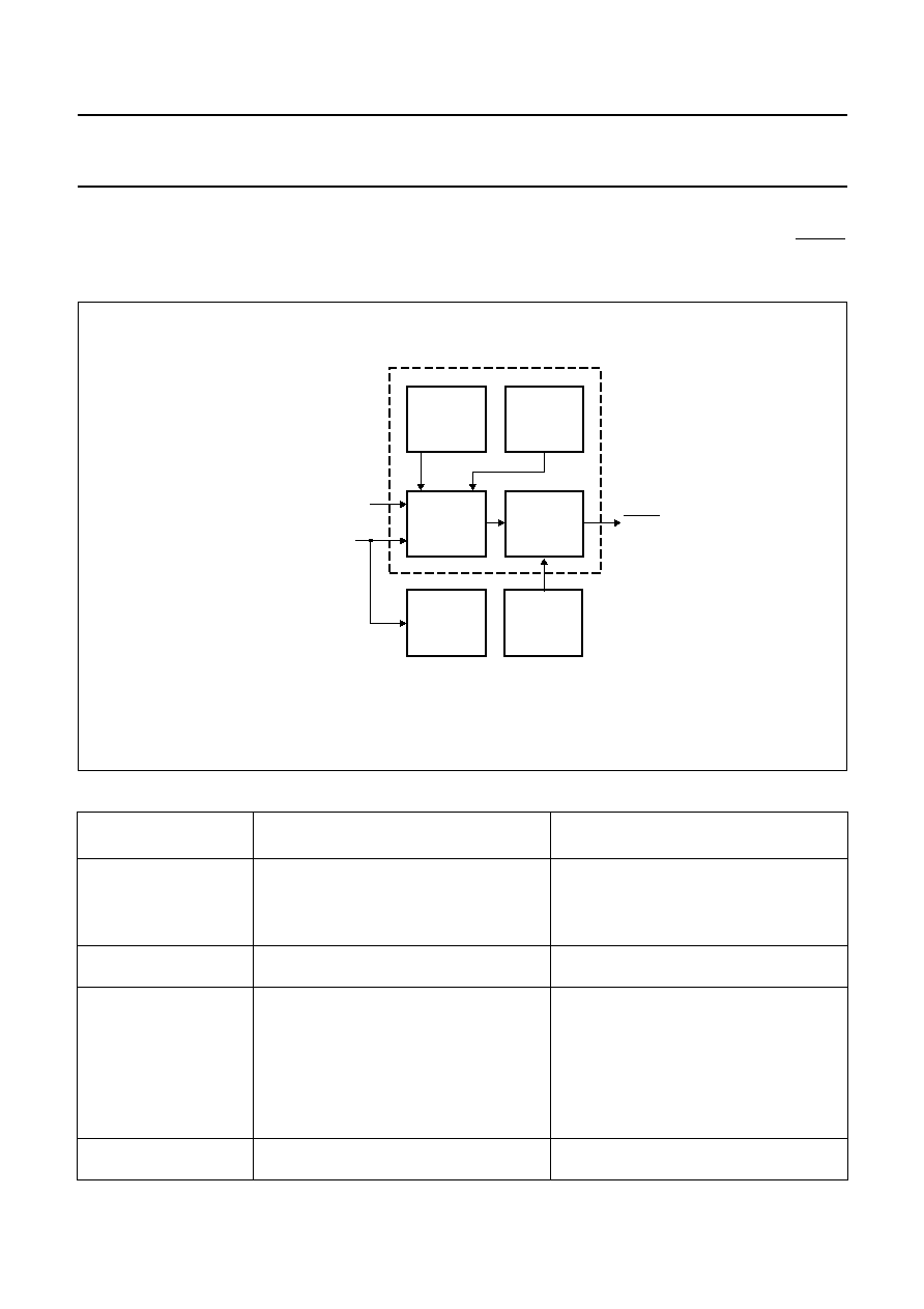
15 CLOCK SYSTEM
15.1
Clock generation circuit
The internal CGC generates the system clocks LLC, LLC2
and the clock reference signal CREF. The internally
generated LFCO (triangular waveform) is multiplied by
four via the analog PLL (including phase detector, loop
filter, VCO and frequency divider). The rectangular output
signals have a 50% duty factor.
Table 4
System clock frequencies
CLOCK
FREQUENCY (MHz)
50 Hz
60 Hz
XTAL
26.8
26.8
LLC
29.5
24.545454
LLC2
14.75
12.272727
LLC4
7.375
6.136136
LLC8
3.6875
3.068181
Fig.18 Clock generation circuit.
handbook, full pagewidth
BAND PASS
FC = LLC/4
ZERO
CROSS
DETECTION
PHASE
DETECTION
LOOP
FILTER
DIVIDER
1/2
DIVIDER
1/2
OSCILLATOR
DELAY
CREF
MGC837
LLC2
LLC
LFCO
1995 Oct 18
29
Philips Semiconductors
Product specification
One Chip Front-end 1 (OCF1)
SAA7110; SAA7110A
15.2
Power-on control
Power-on reset is activated at power-on (using only internal CGC) and if the supply voltage falls below 3.5 V. The RESET
signal can be applied to reset other circuits of the digital TV system.
Table 5
Power-on control sequence
INTERNAL POWER-ON
CONTROL SEQUENCE
PIN OUTPUT STATUS
FUNCTION
Directly after power-on
asynchronous reset
Y7 to Y0, UV7 to UV0, RTCO, PLIN, ODD,
GPSW, SDA, HREF, HS, VS, HCL and HSY
in high impedance state
LLC, LLC2 and CREF in HIGH state
direct switching to high impedance (outputs)
or input mode (I/Os) for 20 to 200 ms
Start synchronous
I
2
C-bus reset sequence
LLC, LLC2 and CREF active
starting I
2
C-bus reset sequence
Status after I
2
C-bus reset Y7 to Y0, UV7 to UV0, HREF and HS held
in high impedance state
VS, HCL and HSY held in input function
mode
SA0DH = 7DH (VTRC = 0, RTSE = 1,
HRMV = 1, SSTB = 0, SECS = 1)
SA0EH = 00H (HPLL = 0, OEHV = 0,
OEYC = 0, CHRS = 0, GPSW = 0)
SA31H = 00H (AOSL 1 : 0 = 00, WIRS = 0,
WRSE = 0, SQPB = 0, VBLKA = 0,
PULIO = 0)
Status after power-on
control sequence
RTCO, PLIN, ODD, GPSW and SDA active
after power-on (reset sequence) a complete
I
2
C-bus transmission is required
Fig.19 Power-on control circuit.
handbook, full pagewidth
POC V
DD
POC
LOGIC
ANALOG
POC V
DD
DIGITAL
MGC838
DELAY
CONTROL
CLOCK I/O
CONTROL
CLOCK
OUTPUT
ACTIVE
CONTROL
CGCE
LLC
RESET
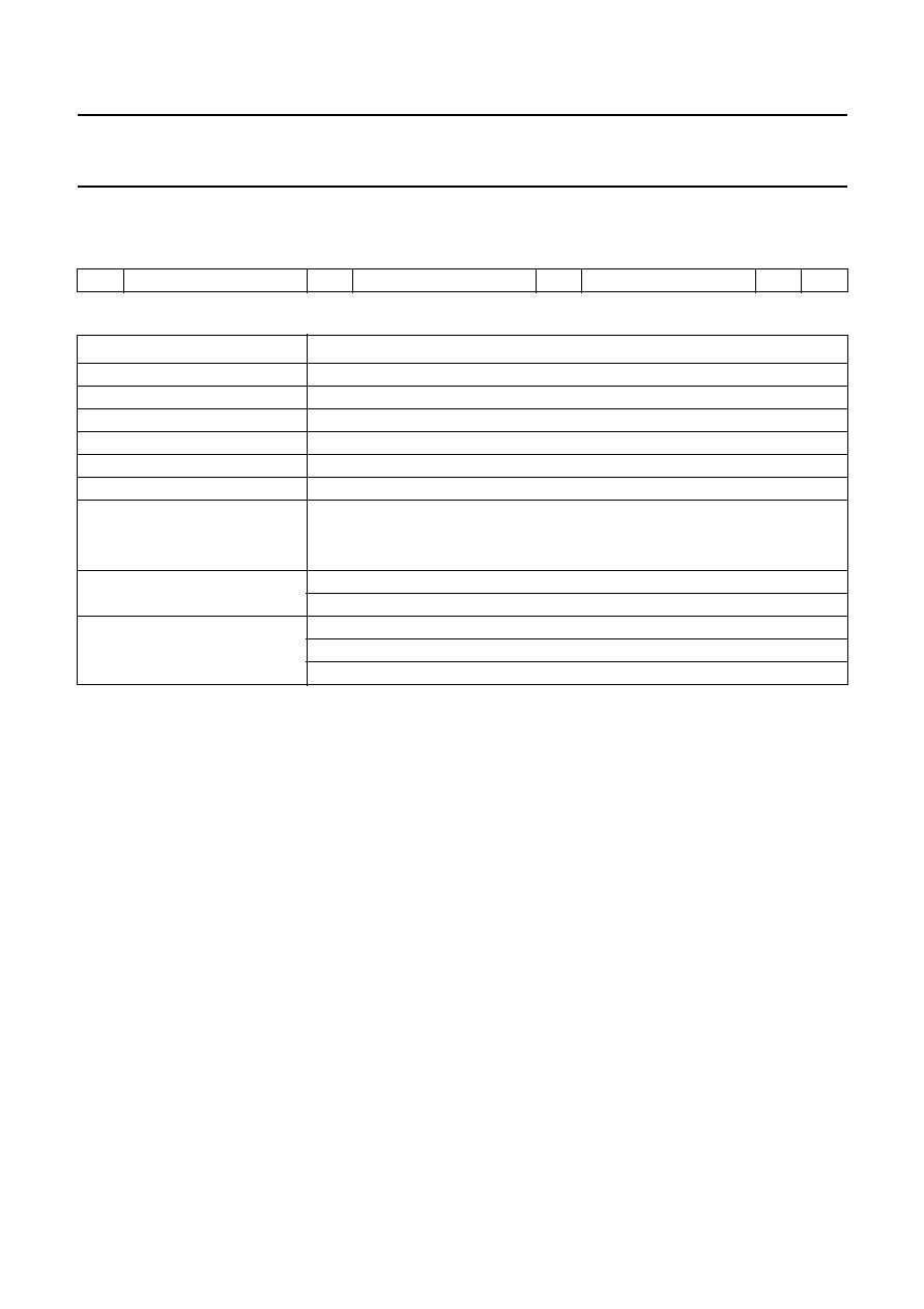
1995 Oct 18
30
Philips Semiconductors
Product specification
One Chip Front-end 1 (OCF1)
SAA7110; SAA7110A
16 I
2
C-BUS DESCRIPTION
16.1
I
2
C-bus format
Table 6
Description of I
2
C-bus format
Note
1. If more than one byte DATA is transmitted then the auto-increment of the subaddress is performed.
S
SLAVE ADDRESS
ACK
SUBADDRESS
ACK
DATA (n bytes)
ACK
P
CODE
DESCRIPTION
S
START condition
Slave address
1001 110Xb (SA = LOW) or 1001 111Xb (SA = HIGH)
ACK
acknowledge generated by the slave
Subaddress
subaddress byte, see Table 7
Data
data byte, see Table 7; note 1
P
STOP condition
X
read/write control bit:
X = 0, order to write (the circuit is slave receiver)
X = 1, order to read (the circuit is slave transmitter)
Slave address
9CH for write, 9DH for read (SA = 0)
9EH for write, 9FH for read (SA = 1
Subaddress
00H to 19H decoder part
1AH to 1FH reserved
20H to 34H front-end part
1995 Oct 18
31
Philips Semiconductors
Product specification
One Chip Front-end 1 (OCF1)
SAA7110; SAA7110A
16.2
I
2
C-bus receiver/transmitter tables
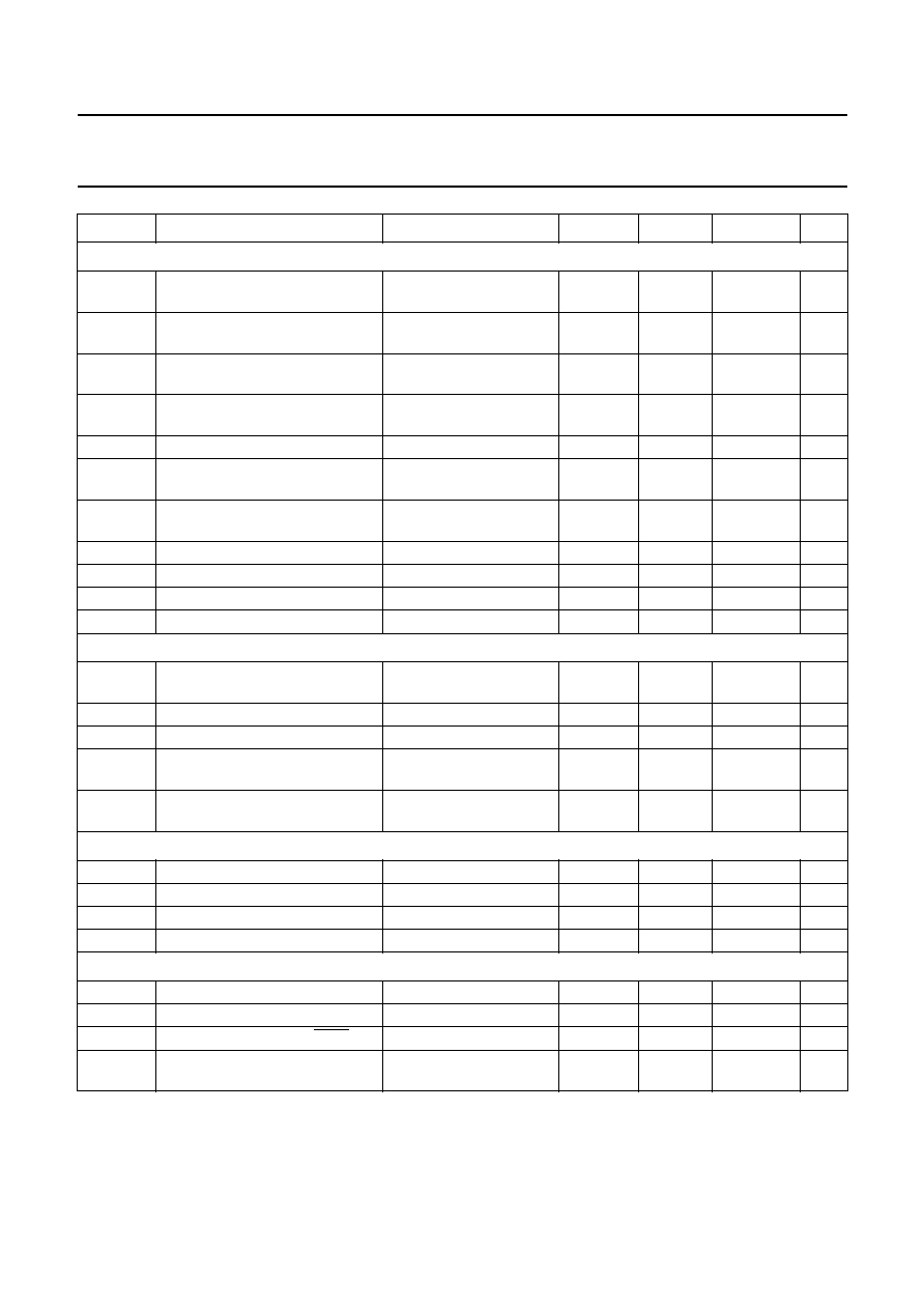
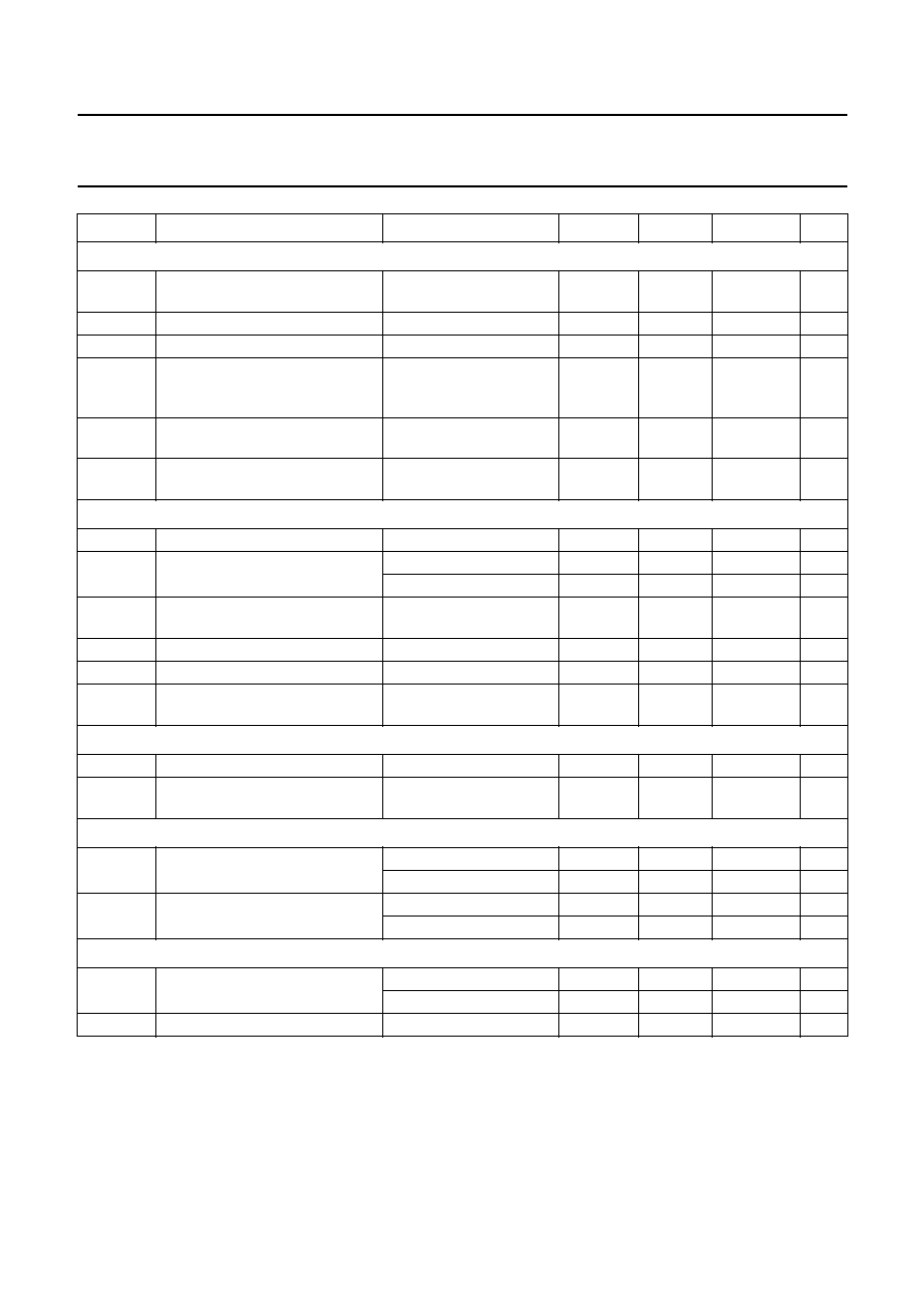
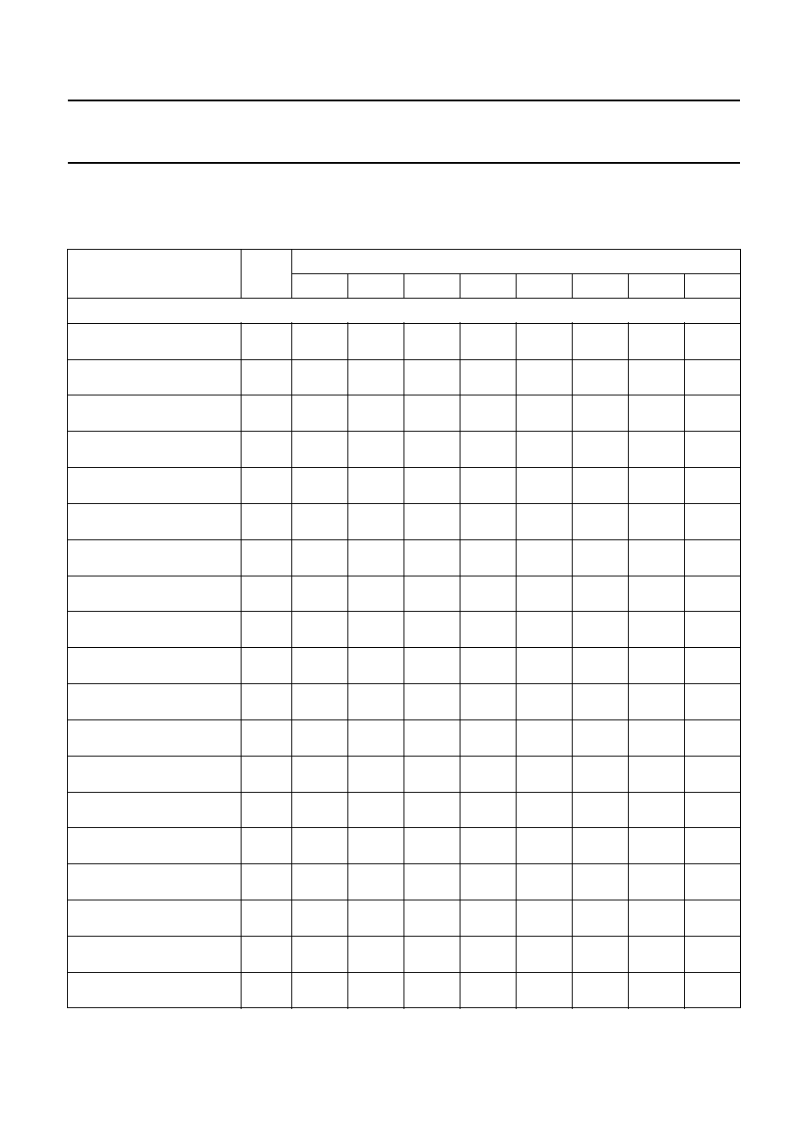
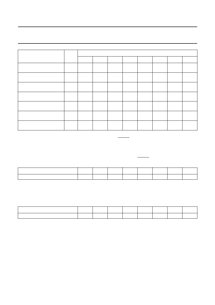
Table 7
OCF1
RECEIVER
Slave address 10011100b, 9CH (SA = 0) and 10011110b, 9EH (SA = 1)
REGISTER FUNCTION
SUB
ADD
(1)
DATA BYTE
(2)
D7
D6
D5
D4
D3
D2
D1
D0
DMSD-SQP + BSC slave receiver (SU 00H to 19H)
Increment delay
00
007
IDEL7
006
IDEL6
005
IDEL5
004
IDEL4
003
IDEL3
002
IDEL2
001
IDEL1
000
IDEL0
HSY begin 50 Hz
01
015
HSYB7
014
HSYB6
013
HSYB5
012
HSYB4
011
HSYB3
010
HSYB2
009
HSYB1
008
HSYB0
HSY stop 50 Hz
02
023
HSYS7
022
HSYS6
021
HSYS5
020
HSYS4
019
HSYS3
018
HSYS2
017
HSYS1
016
HSYS0
HCL begin 50 Hz
03
031
HCLB7
030
HCLB6
029
HCLB5
028
HCLB4
027
HCLB3
026
HCLB2
025
HCLB1
024
HCLB0
HCL stop 50 Hz
04
039
HCLS7
038
HCLS6
037
HCLS5
036
HCLS4
035
HCLS3
034
HCLS2
033
HCLS1
032
HCLS0
HSY after PHI1 50 Hz
05
047
HPHI7
046
HPHI6
045
HPHI5
044
HPHI4
043
HPHI3
042
HPHI2
041
HPHI1
040
HPHI0
Luminance control
06
055
BYPS
054
PREF
053
BPSS1
052
BPSS0
051
CORI1
050
CORI0
049
APER1
048
APER0
Hue control
07
063
HUEC7
062
HUEC6
061
HUEC5
060
HUEC4
059
HUEC3
058
HUEC2
057
HUEC1
056
HUEC0
Colour killer threshold
QUAM (PAL/NTSC)
08
071
CKTQ4
070
CKTQ3
069
CKTQ2
068
CKTQ1
067
CKTQ0
066
XXX
065
XXX
064
XXX
Colour killer threshold
SECAM
09
079
CKTS4
078
CKTS3
077
CKTS2
076
CKTS1
075
CKTS0
074
XXX
073
XXX
072
XXX
PAL switch sensitivity
0A
087
PLSE7
086
PLSE6
085
PLSE5
084
PLSE4
083
PLSE3
082
PLSE2
081
PLSE1
080
PLSE0
SECAM switch sensitivity
0B
095
SESE7
094
SESE6
093
SESE5
092
SESE4
091
SESE3
090
SESE2
089
SESE1
088
SESE0
Gain control chrominance
0C
103
COLO
102
LFIS1
101
LFIS0
100
XXX
099
XXX
098
XXX
097
XXX
096
XXX
Standard/mode control
0D
111
VTRC
110
XXX
109
XXX
108
XXX
107
RTSE
106
HRMV
105
SSTB
104
SECS
I/O and clock control
0E
119
HPLL
118
XXX
117
XXX
116
OEHV
115
OEYC
114
CHRS
113
XXX
112
GPSW
Control #1
0F
127
AUFD
126
FSEL
125
SXCR
124
SCEN
123
XXX
122
YDEL2
121
YDEL1
120
YDEL0
Control #2
10
135
XXX
134
XXX
133
XXX
132
XXX
131
XXX
130
HRFS
129
VNOI1
128
VNOI0
Chrominance gain reference
11
143
CHCV7
142
CHCV6
141
CHCV5
140
CHCV4
139
CHCV3
138
CHCV2
137
CHCV1
136
CHCV0
Chrominance saturation
12
151
SATN7
150
SATN6
149
SATN5
148
SATN4
147
SATN3
146
SATN2
145
SATN1
144
SATN0
1995 Oct 18
32
Philips Semiconductors
Product specification
One Chip Front-end 1 (OCF1)
SAA7110; SAA7110A
Luminance contrast
13
159
CONT7
158
CONT6
157
CONT5
156
CONT4
155
CONT3
154
CONT2
153
CONT1
152
CONT0
HSY begin 60 Hz
14
167
HS6B7
166
HS6B6
165
HS6B5
164
HS6B4
163
HS6B3
162
HS6B2
161
HS6B1
160
HS6B0
HSY stop 60 Hz
15
175
HS6S7
174
HS6S6
173
HS6S5
172
HS6S4
171
HS6B3
170
HS6S2
169
HS6S1
168
HS6S0
HCL begin 60 Hz
16
183
HC6B7
182
HC6B6
181
HC6B5
180
HCLB4
179
HC6B3
178
HC6B2
177
HC6B1
176
HC6B0
HCL stop 60 Hz
17
191
HC6S7
190
HC6S6
189
HC6S5
188
HC6S4
187
HC6S3
186
HC6S2
185
HC6S1
184
HC6S0
HSY after PHI1 60 Hz
18
199
HP6I7
198
HP6I6
197
HP6I5
196
HP6I4
195
HP6I3
194
HP6I2
193
HP6I1
192
HP6I0
Luminance brightness
19
207
BRIG7
206
BRIG6
205
BRIG5
204
BRIG4
203
BRIG3
202
BRIG2
201
BRIG1
200
BRIG0
DUAD slave receiver (SU 20H to 32H)
Analog control #1
20
007
AIND4
006
AIND3
005
AIND2
004
FUSE1
003
FUSE0
002
AINS4
001
AINS3
000
AINS2
Analog control #2
21
015
VBCO
014
MS34
013
MX241
012
MX240
011
MS24
010
REFS4
009
REFS3
008
REFS2
Mixer control #1
22
023
GACO1
022
GACO0
021
CSEL
020
YSEL
019
MUYC
018
CLTS
017
MX341
016
MX340
Clamping level control 21
23
031
CLL217
030
CLL216
029
CLL215
028
CLL214
027
CLL213
026
CLL212
025
CLL211
024
CLL210
Clamping level control 22
24
039
CLL227
038
CLL226
037
CLL225
036
CLL224
035
CLL223
034
CLL222
033
CLL221
032
CLL220
Clamping level control 31
25
047
CLL317
046
CLL316
045
CLL315
044
CLL314
043
CLL313
042
CLL312
041
CLL311
040
CLL310
Clamping level control 32
26
055
CLL327
054
CLL326
053
CLL325
052
CLL324
051
CLL323
050
CLL322
049
CLL321
048
CLL320
Gain control analog #1
27
063
HOLD
062
GASL
061
GAI25
060
GAI24
059
GAI23
058
GAI22
057
GAI21
056
GAI20
White peak control
28
071
WIPE7
070
WIPE6
069
WIPE5
068
WIPE4
067
WIPE3
066
WIPE2
065
WIPE1
064
WIPE0
Sync bottom control
29
079
SBOT7
078
SBOT6
077
SBOT5
076
SBOT4
075
SBOT3
074
SBOT2
073
SBOT1
072
SBOT0
Gain control analog #2
2A
087
IWIP1
086
IWIP0
085
GAI35
084
GAI34
083
GAI33
082
GAI32
081
GAI31
080
GAI30
Gain control analog #3
2B
095
IGAI1
094
IGAI0
093
GAI45
092
GAI44
091
GAI43
090
GAI42
089
GAI41
088
GAI40
Mixer control #2
2C
103
CLS4
102
XXX
101
CLS3
100
CLS2
099
XXX
098
XXX
097
TWO3
096
TWO2
Integration value gain
2D
111
IVAL7
110
IVAL6
109
IVAL5
108
IVAL4
107
IVAL3
106
IVAL2
105
IVAL1
104
IVAL0
REGISTER FUNCTION
SUB
ADD
(1)
DATA BYTE
(2)
D7
D6
D5
D4
D3
D2
D1
D0
1995 Oct 18
33
Philips Semiconductors
Product specification
One Chip Front-end 1 (OCF1)
SAA7110; SAA7110A
Notes
1. Subaddresses to be reset: 0D to 7DH, 0E and 31 to 00H after RESET = 0 (CGCE = 0) or power-on (CGCE = 1).
2. All reserved XXX-bits must be set to LOW, XX-bit is don't care.
3. AFCCS bit does not exist in SAA7110A due to advanced anti-alias filter characteristic, don't care (XX).
Table 8
OCF1
TRANSMITTER
: Byte number 0 (transmitted if SSTB = 0 or after RESET has been 0)
Slave address 10011101b, 9DH (SA = 0) and 10011111b, 9FH (SA = 1
Note
1. ID7 to ID0 indicates the version number of the IC, for example SAA7110A V1 = 01H.
Table 9
OCF1
TRANSMITTER
: Byte number 1 (transmitted if SSTB = 1)
Slave address 10011101b, 9DH (SA = 0) and 10011111b, 9FH (SA = 1)
Vertical blanking pulse set
2E
119
VBPS7
118
VBPS6
117
VBPS5
116
VBPS4
115
VBPS3
114
VBPS2
113
VBPS1
112
VBPS0
Vertical blanking pulse reset
2F
127
VBPR7
126
VBPR6
125
VBPR5
124
VBPR4
123
VBPR3
122
VBPR2
121
VBPR1
120
VBPR0
ADCs gain control
30
135
XXX
134
WISL
133
GAS3
132
GAD31
131
GAD30
130
GAS2
129
GAD21
128
GAD20
Mixer control #3
31
143
AOSL1
142
AOSL0
141
WIRS
140
WRSE
139
SQPB
138
(3)
AFCCS
137
VBLKA
136
PULIO
Integration value white peak
32
151
WVAL7
150
WVAL6
149
WVAL5
148
WVAL4
147
WVAL3
146
WVAL2
145
WVAL1
144
WVAL0
Mixer control #4
33
159
OFTS
158
XXX
157
CHSB
156
XXX
155
CAD3
154
CAD2
153
XXX
152
XXX
Gain update level
34
167
MUD2
166
MUD1
165
GUDL5
164
GUDL4
163
GUDL3
162
GUDL2
161
GUDL1
160
GUDL0
VERSION STATUS BYTE
D7
D6
D5
D4
D3
D2
D1
D0
ID7 to ID0; note 1
ID7
ID6
ID5
ID4
ID3
ID2
ID1
ID0
STATUS BYTE FUNCTION
D7
D6
D5
D4
D3
D2
D1
D0
See Table 10 for explanation of bits
STTC
HLCK
FIDT
GLIM
XXX
WIPA
ALTD
CODE
REGISTER FUNCTION
SUB
ADD
(1)
DATA BYTE
(2)
D7
D6
D5
D4
D3
D2
D1
D0

1995 Oct 18
34
Philips Semiconductors
Product specification
One Chip Front-end 1 (OCF1)
SAA7110; SAA7110A
Table 10 Explanation of bits shown in Table 9
16.3
I
2
C-bus detail
The I
2
C-bus receiver slave address is 9CH/9EH.
DMSD-SQP slave receiver (SU 00H to 19H).
16.3.1
S
UBADDRESS
00 (
DATA BYTE
007 to 000)
Table 11 Increment delay IDEL
Notes
1. A sign bit, designated A08 and internally set to HIGH, indicates values are always negative.
2. The horizontal PLL does not operate in this condition. The system clock frequency is set to a value fixed by the last
update and is within
±
7.1% of the nominal frequency.
BIT
DESCRIPTION
STTC
Status bit for horizontal time constant: LOW = TV time constant; HIGH = VCR time constant.
HLCK
Status bit for locked horizontal frequency: LOW = locked; HIGH = unlocked.
FIDT
Identification bit for detected field frequency: LOW = 50 Hz; HIGH = 60 Hz.
GLIM
Gain value for active luminance is limited (maximum or minimum), active HIGH.
XXX
reserved
WIPA
White peak loop is activated, active HIGH.
ALTD
Status HIGH: line alternating colour burst has been detected (PAL or SECAM).
CODE
Status HIGH: any colour signal has been detected.
DECIMAL
MULTIPLIER
DELAY TIME
(STEP SIZE = 4/LLC)
CONTROL BITS
(1)
IDEL7
IDEL6
IDEL5
IDEL4
IDEL3
IDEL2
IDEL1
IDEL0
-
1
-
4
1
1
1
1
1
1
1
1
-
195
-
780
max. value for 60 Hz
0
0
1
1
1
1
0
1
-
236
-
944
max. value for 50 Hz
0
0
0
1
0
1
0
0
-
256
-
1024
outside central counter
(2)
0
0
0
0
0
0
0
0
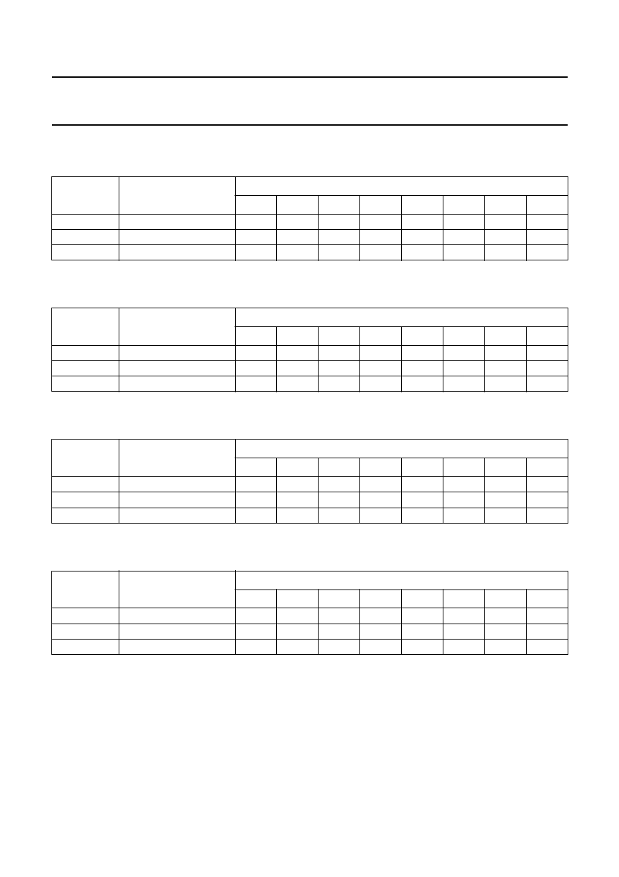
1995 Oct 18
35
Philips Semiconductors
Product specification
One Chip Front-end 1 (OCF1)
SAA7110; SAA7110A
16.3.2
S
UBADDRESS
01 (
DATA BYTE
015 to 008)
Table 12 Horizontal synchronization begin 50 Hz (HSYB)
16.3.3
S
UBADDRESS
02 (
DATA BYTE
023 to 016)
Table 13 Horizontal synchronization stop 50 Hz (HSYS)
16.3.4
S
UBADDRESS
03 (
DATA BYTE
031 to 024)
Table 14 Horizontal clamping begin 50 Hz (HCLB)
16.3.5
S
UBADDRESS
04 (
DATA BYTE
039 to 032)
Table 15 Horizontal clamping stop 50 Hz (HCLS)
DECIMAL
MULTIPLIER
DELAY TIME
(STEP SIZE = 2/LLC)
CONTROL BITS
HSYB7 HSYB6 HSYB5 HSYB4 HSYB3 HSYB2 HSYB1 HSYB0
+191
-
382
1
0
1
1
1
1
1
1
-
64
+128
1
1
0
0
0
0
0
0
DECIMAL
MULTIPLIER
DELAY TIME
(STEP SIZE = 2/LLC)
CONTROL BITS
HSYS7
HSYS6
HSYS5
HSYS4
HSYS3
HSYS2
HSYS1
HSYS0
+191
-
382
1
0
1
1
1
1
1
1
-
64
+128
1
1
0
0
0
0
0
0
DECIMAL
MULTIPLIER
DELAY TIME
(STEP SIZE = 2/LLC)
CONTROL BITS
HCLB7 HCLB6 HCLB5 HCLB4 HCLB3 HCLB2 HCLB1 HCLB0
+127
-
254
0
1
1
1
1
1
1
1
-
128
+256
1
0
0
0
0
0
0
0
DECIMAL
MULTIPLIER
DELAY TIME
(STEP SIZE = 2/LLC)
CONTROL BITS
HCLS7
HCLS6
HCLS5
HCLS4
HCLS3
HCLS2
HCLS1
HCLS0
+127
-
254
0
1
1
1
1
1
1
1
-
128
+256
1
0
0
0
0
0
0
0
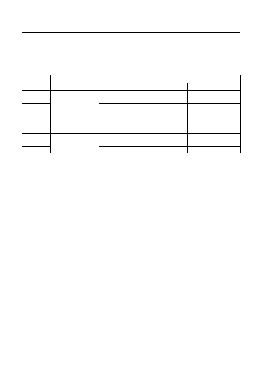
1995 Oct 18
36
Philips Semiconductors
Product specification
One Chip Front-end 1 (OCF1)
SAA7110; SAA7110A
16.3.6
S
UBADDRESS
05 (
DATA BYTE
047 to 040)
Table 16 Horizontal synchronization start after PHI1 50 Hz (HPHI)
DECIMAL
MULTIPLIER
DELAY TIME
(STEP SIZE = 8/LLC)
CONTROL BITS
HPHI7
HPHI6
HPHI5
HPHI4
HPHI3
HPHI2
HPHI1
HPHI0
+127
forbidden;
outside available central
counter range
0
1
1
1
1
1
1
1
+118
0
1
1
1
0
1
1
0
+117
-
32
µ
s
(max. negative value)
0
1
1
1
0
1
0
1
-
118
+31.7
µ
s
(max. positive value)
1
0
0
0
1
0
1
0
-
119
forbidden;
outside available central
counter range
1
0
0
0
1
0
0
1
-
128
1
0
0
0
0
0
0
0
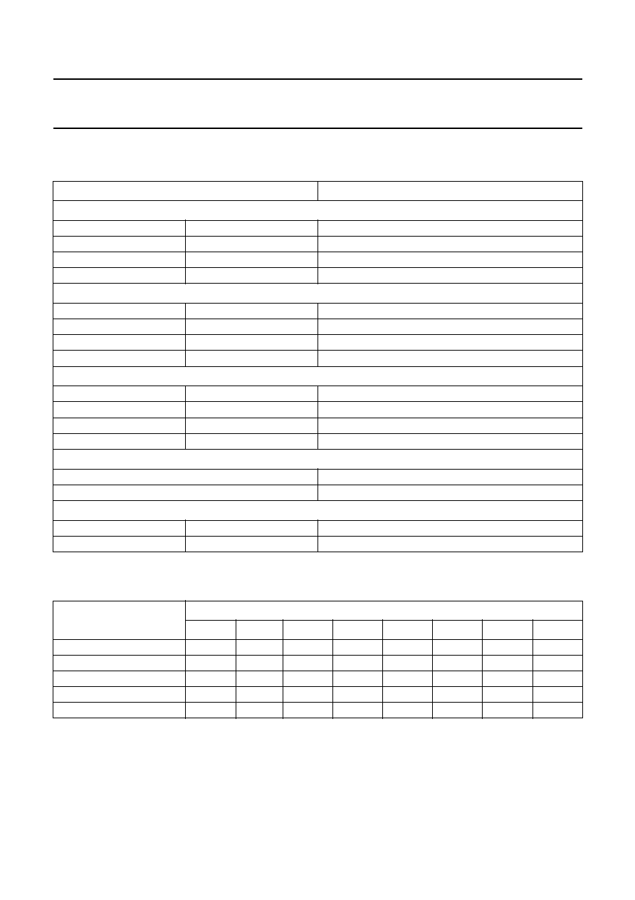
1995 Oct 18
37
Philips Semiconductors
Product specification
One Chip Front-end 1 (OCF1)
SAA7110; SAA7110A
16.3.7
S
UBADDRESS
06 (
DATA BYTE
055 to 048)
Table 17 Luminance control
16.3.8
S
UBADDRESS
07 (
DATA BYTE
063 to 056)
Table 18 Hue phase control HUEC
FUNCTION
CONTROL BITS
Aperture factor (APER); data bits D1 and D0
0
0
APER1 = 0; APER0 = 0
1
0.25
APER1 = 0; APER0 = 1
2
0.5
APER1 = 1; APER0 = 0
3
1.0
APER1 = 1; APER0 = 1
Corner correction (CORI)
±
LSBs in 8-bit; data bits D3 and D2
0
0 (OFF)
CORI1 = 0; CORI0 = 0
1
1
CORI1 = 0; CORI0 = 1
2
2
CORI1 = 1; CORI0 = 0
3
3
CORI1 = 1; CORI0 = 1
Aperture bandpass; centre frequency (BPSS); data bits D4 and D5
4.6 MHz (50 Hz)
3.8 MHz (60 Hz)
BPSS1 = 0; BPSS0 = 0
4.3 MHz (50 Hz)
3.4 MHz (60 Hz)
BPSS1 = 0; BPSS0 = 1
3.0 MHz (50 Hz)
2.5 MHz (60 Hz)
BPSS1 = 1; BPSS0 = 0
3.2 MHz (50 Hz)
2.7 MHz (60 Hz)
BPSS1 = 1; BPSS0 = 1
Prefilter active (PREF); data bit D6
Bypassed
PREF = 0
Active
PREF = 1
Chrominance trap bypass (BYPS); data bit D7
Active
CVBS mode
BYPS = 0
Bypassed
S-Video mode
BYPS = 1
HUE PHASE (DEGREES)
CONTROL BITS
HUEC7
HUEC6
HUEC5
HUEC4
HUEC3
HUEC2
HUEC1
HUEC0
+178.6
0
1
1
1
1
1
1
1
0
0
0
0
0
0
0
0
0
-
180
1
0
0
0
0
0
0
0
1995 Oct 18
38
Philips Semiconductors
Product specification
One Chip Front-end 1 (OCF1)
SAA7110; SAA7110A
16.3.9
S
UBADDRESS
08 C
ONTROL NUMBER
1 (
DATA BYTE
071 to 064)
Table 19 Colour killer threshold QUAM (PAL/NTSC)
16.3.10 S
UBADDRESS
09 C
ONTROL NUMBER
2 (
DATA BYTE
079 to 072)
Table 20 Colour killer threshold SECAM
16.3.11 S
UBADDRESS
0A (
DATA BYTE
087 to 080)
Table 21 PAL switch sensitivity
Note
1. Sensitivity HIGH means immediate sequence correction.
16.3.12 S
UBADDRESS
0B (
DATA BYTE
095 to 088)
Table 22 SECAM switch sensitivity
Note
1. Sensitivity HIGH means immediate sequence correction.
THRESHOLD
(reference is nominal burst amplitude = 0 dB)
CONTROL BITS
CKTQ4
CKTQ3
CKTQ2
CKTQ1
CKTQ0
-
30 dB
1
1
1
1
1
-
24 dB
1
0
0
0
0
-
18 dB
0
0
0
0
0
THRESHOLD
(reference is nominal burst amplitude = 0 dB)
CONTROL BITS
CKTS4
CKTS3
CKTS2
CKTS1
CKTS0
-
30 dB
1
1
1
1
1
-
24 dB
1
0
0
0
0
-
18 dB
0
0
0
0
0
SENSITIVITY
CONTROL BITS
PLSE7
PLSE6
PLSE5
PLSE4
PLSE3
PLSE2
PLSE1
PLSE0
Low
1
1
1
1
1
1
1
1
Medium
1
0
0
0
0
0
0
0
High
(1)
0
0
0
0
0
0
0
0
SENSITIVITY
CONTROL BITS
SESE7
SESE6
SESE5
SESE4
SESE3
SESE2
SESE1
SESE0
Low
1
1
1
1
1
1
1
1
Medium
1
0
0
0
0
0
0
0
High
(1)
0
0
0
0
0
0
0
0

1995 Oct 18
39
Philips Semiconductors
Product specification
One Chip Front-end 1 (OCF1)
SAA7110; SAA7110A
16.3.13 S
UBADDRESS
0C (
DATA BYTE
103 to 096)
Table 23 Gain control chrominance
16.3.14 S
UBADDRESS
0D (
DATA BYTE
111 to 104)
Table 24 Standard/mode control
FUNCTION
CONTROL BITS
AGC loop filter (LFIS); data bits D6 and D5
Slow time constant
LFIS1 = 0; LFIS0 = 0
Medium time constant
LFIS1 = 0; LFIS0 = 1
Fast time constant
LFIS1 = 1; LFIS0 = 0
Actual chrominance gain frozen
LFIS1 = 1; LFIS0 = 1
Colour on (COLO); data bit D7
Automatic colour killer
COLO = 0
Colour forced on
COLO = 1
FUNCTION
CONTROL BITS
SECAM mode bit (SECS); data bit D0
Other standards
SECS = 0
SECAM mode
SECS = 1
Status byte select (SSTB); data bit D1
Status byte = 0 (see transmitter)
SSTB 0
Status byte = 1 (see transmitter)
SSTB = 1
HREF position select (HRMV); data bit D2
HREF position as SAA7191 (8 LLC2 later)
HRMV = 0
HREF normal position
HRMV = 1
Real time outputs mode select (RTSE); data bit D3
PLIN switched to output pin 39
ODD switched to output pin 40
RTSE = 0
HL switched to output pin 39 VL switched to output pin 40
RTSE = 1
TV/VCR mode select (VTRC); data bit D7
TV mode
VTRC = 0
VTR mode
VTRC = 1

1995 Oct 18
40
Philips Semiconductors
Product specification
One Chip Front-end 1 (OCF1)
SAA7110; SAA7110A
16.3.15 S
UBADDRESS
0E (
DATA BYTE
119 to 112)
Table 25 I/O and clock control
16.3.16 S
UBADDRESS
0F (
DATA BYTE
127 to 120)
Table 26 Control number 1
FUNCTION
CONTROL BITS
General purpose switch (GPSW); data bit D0
Switches directly pin 64 GPSW (application dependent);
VBLKA = 0
GPSW = 0
GPSW = 1
Select chrominance input (CHRS); data bit D2
Controlled by BYPS (subaddress 06) normal position
CHRS = 0
Digital chrominance input switched to
second input channel (see Fig.20)
CHRS = 1
Output enable YUV-data (OEYC); data bit D3
YUV bus high impedance/input
OEYC = 0
Output YUV-bus active
OEYC = 1
Output enable horizontal/vertical synchronization (OEHV); data bit D4
HS, HREF and VS high impedance/inputs
OEHV = 0
Output HS, HREF and VS active
OEHV = 1
Horizontal PLL clock (HPLL); data bit D7
PLL closed
HPLL = 0
PLL open, horizontal frequency fixed
HPLL = 1
FUNCTION
CONTROL BITS
Luminance delay compensation; steps in 2/LLC (YDEL); data bits D2, D1 and D0
0 steps
YDEL2 = 0; YDEL1 = 0; YDEL0 = 0
3 steps
YDEL2 = 0; YDEL1 = 1; YDEL0 = 1
-
4 steps
YDEL2 = 1; YDEL1 = 0 YDEL1 = 0
Enable or disable of sync and clamp pulses; HSY and HCL (SCEN); data bit D4
Disable sync and clamp (set to HIGH)
SCEN = 0
Enable sync and clamp
SCEN = 1
SECAM cross colour reduction (SXCR); data bit D5
Reduction off
SXCR = 0
Reduction on
SXCR = 1
Field selection (FSEL); data bit D6
50 Hz, 625 lines
FSEL = 0
60 Hz, 525 lines
FSEL = 1
Automatic field detection(AUFD); data bit D7
Field state directly controlled via FSEL
AUFD = 0
Automatic field detection
AUFD = 1

1995 Oct 18
41
Philips Semiconductors
Product specification
One Chip Front-end 1 (OCF1)
SAA7110; SAA7110A
16.3.17 S
UBADDRESS
10 (
DATA BYTE
135 to 128)
Table 27 Control number 2
16.3.18 S
UBADDRESS
11 (
DATA BYTE
143 to 136)
Table 28 Chrominance gain reference value
16.3.19 S
UBADDRESS
12 (
DATA BYTE
150 to 144)
Table 29 Chrominance saturation control
FUNCTION
CONTROL BITS
Vertical noise reduction (VNOI); data bits D1 and D0
Normal mode
VNOI1 = 0; VNOI0 = 0
Search mode
VNOI1 = 0; VNOI0 = 1
Free running mode
VNOI1 = 1; VNOI0 = 0
Vertical noise reduction bypassed
VNOI1 = 1; VNOI0 = 1
HREF select HRFS (HRFS); data bit D2
HREF matched to YUV output
HRFS = 0
HREF matched to CVBS input
HRFS = 1
REFERENCE VALUE
CONTROL BITS
CHCV7
CHCV6
CHCV5
CHCV4
CHCV3
CHCV2
CHCV1
CHCV0
Maximum
1
1
1
1
1
1
1
1
CCIR-level for PAL
0
1
0
1
1
0
0
1
CCIR-level for NTSC
0
0
1
0
1
1
0
0
Minimum
0
0
0
0
0
0
0
0
GAIN
CONTROL BITS
SATN7
SATN6
SATN5
SATN4
SATN3
SATN2
SATN1
SATN0
1.999 Maximum
0
1
1
1
1
1
1
1
1 CCIR-level
0
1
0
0
0
0
0
0
0 colour off
0
0
0
0
0
0
0
0
-
1 inverse chrominance
1
1
0
0
0
0
0
0
-
2 inverse chrominance
1
0
0
0
0
0
0
0
1995 Oct 18
42
Philips Semiconductors
Product specification
One Chip Front-end 1 (OCF1)
SAA7110; SAA7110A
16.3.20 S
UBADDRESS
13 (
DATA BYTE
158 to 152)
Table 30 Luminance contrast control
16.3.21 S
UBADDRESS
14 (
DATA BYTE
167 to 160)
Table 31 Horizontal synchronization begin 60 Hz (HS6B)
16.3.22 S
UBADDRESS
15 (
DATA BYTE
175 to 168)
Table 32 Horizontal synchronization stop 60 Hz (HS6S)
16.3.23 S
UBADDRESS
16 (
DATA BYTE
183 to 176)
Table 33 Horizontal clamping begin 60 Hz (HC6B)
GAIN
CONTROL BITS
CONT7 CONT6 CONT5
CONT4
CONT3
CONT2
CONT1
CONT0
1.999 Maximum
0
1
1
1
1
1
1
1
70 CCIR-level
0
1
0
0
0
1
1
0
1
0
1
0
0
0
0
0
0
0 luminance off
0
0
0
0
0
0
0
0
-
1 inverse luminance
1
1
0
0
0
0
0
0
-
2 inverse luminance
1
0
0
0
0
0
0
0
DECIMAL
MULTIPLIER
DELAY TIME
(step size = 2/LLC)
CONTROL BITS
HS6B7
HS6B6
HS6B5
HS6B4
HS6B3
HS6B2
HS6B1
HS6B0
+191
-
382
1
0
1
1
1
1
1
1
-
64
+128
1
1
0
0
0
0
0
0
DECIMAL
MULTIPLIER
DELAY TIME
(step size = 2/LLC)
CONTROL BITS
HS6S7
HS6S6
HS6S5
HS6S4
HS6S3
HS6S2
HS6S1
HS6S0
+191
-
382
1
0
1
1
1
1
1
1
-
64
+128
1
1
0
0
0
0
0
0
DECIMAL
MULTIPLIER
DELAY TIME
(step size = 2/LLC)
CONTROL BITS
HC6B7
HC6B6
HC6B5
HC6B4
HC6B3
HC6B2
HC6B1
HC6B0
+127
-
254
0
1
1
1
1
1
1
1
-
128
+256
1
0
0
0
0
0
0
0
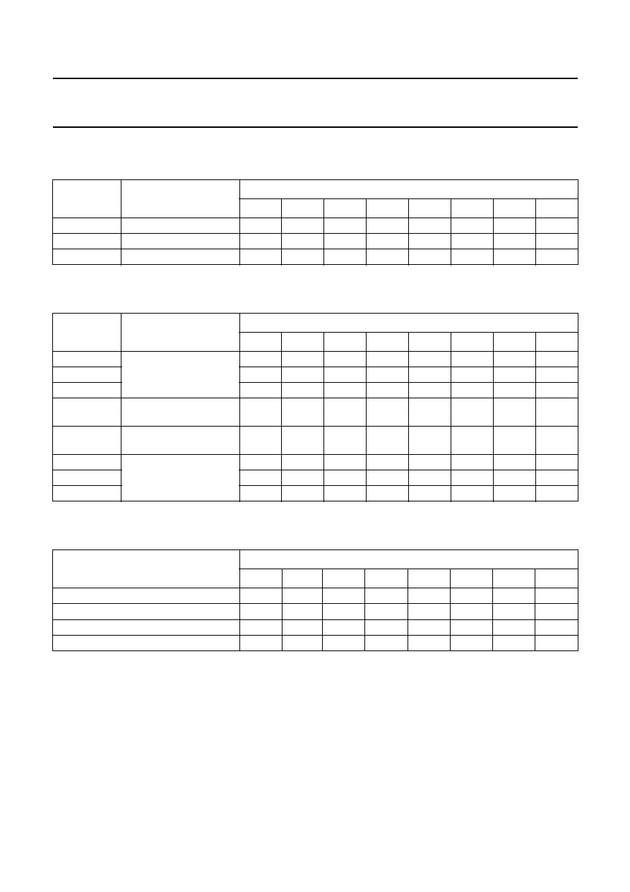
1995 Oct 18
43
Philips Semiconductors
Product specification
One Chip Front-end 1 (OCF1)
SAA7110; SAA7110A
16.3.24 S
UBADDRESS
17 (
DATA BYTE
191 to 184)
Table 34 Horizontal clamping stop 60 Hz (HC6S)
16.3.25 S
UBADDRESS
18 (
DATA BYTE
199 to 192)
Table 35 Horizontal synchronization start after PHI1 60 Hz (HP6I)
16.3.26 S
UBADDRESS
19 (
DATA BYTE
207 to 200)
Table 36 Luminance brightness control
DECIMAL
MULTIPLIER
DELAY TIME
(step size = 2/LLC)
CONTROL BITS
HC6S7
HC6S6
HC6S5
HC6S4
HC6S3
HC6S2
HC6S1
HC6S0
+127
-
254
0
1
1
1
1
1
1
1
-
128
+256
1
0
0
0
0
0
0
0
DECIMAL
MULTIPLIER
DELAY TIME
(step size = 8/LLC)
CONTROL BITS
HP6I7
HP6I6
HP6I5
HP6I4
HP6I3
HP6I2
HP6I1
HP6I0
+127
forbidden;
outside available central
counter range
0
1
1
1
1
1
1
1
+98
0
1
1
0
0
0
1
0
+97
-
32
µ
s
(max. negative value)
0
1
1
0
0
0
0
1
-
97
+31.7
µ
s
(max. positive value)
1
0
0
1
1
1
1
1
-
98
forbidden;
outside available central
counter range
1
0
0
1
1
1
1
0
-
128
1
0
0
0
0
0
0
0
OFFSET
CONTROL BITS
BRIG7
BRIG6
BRIG5
BRIG4
BRIG3
BRIG2
BRIG1
BRIG0
255 (bright)
1
1
1
1
1
1
1
1
139 (CCIR-level)
1
0
0
0
1
0
1
1
128
1
0
0
0
0
0
0
0
0 (dark)
0
0
0
0
0
0
0
0
1995 Oct 18
44
Philips Semiconductors
Product specification
One Chip Front-end 1 (OCF1)
SAA7110; SAA7110A
16.4
I
2
C-bus detail (continued)
DUAD slave receiver (SU 20H to 32H).
16.4.1
S
UBADDRESS
20 (
DATA BYTE
007 to 000)
Table 37 Analog control #1
FUNCTION
CONTROL BITS
Analog input select 2 (AINS2); data bit D0
Analog input AI22 selected
AINS2 = 0
Analog input AI21 selected
AINS2 = 1
Analog input select 3 (AINS3); data bit D1
Analog input AI32 selected
AINS3 = 0
Analog input AI31 selected
AINS3 = 1
Analog input select 4 (AINS4); data bit D2
Analog input AI42 selected
AINS4 = 0
Analog input AI41 selected
AIND4 = 1
Analog function select (FUSE); data bits D4 and D3
Amplifier plus anti-alias filter bypassed
FUSE1 = 0; FUSE0 = 0
FUSE1 = 0; FUSE0 = 1
Amplifier active
FUSE1 = 1; FUSE0 = 0
Amplifier plus anti-alias filter active
FUSE1 = 1; FUSE0 = 1
Analog input disable 2 (AIND2); data bit D5
Analog inputs 2 enabled
AIND2 = 0
Analog inputs 2 disabled
AIND2 = 1
Analog input disable 3 (AIND3); data bit D6
Analog inputs 3 enabled
AIND3 = 0
Analog inputs 3 disabled
AIND3 = 1
Analog input disable 4 (AIND4); data bit D7
Analog inputs 4 enabled
AIND4 = 0
Analog inputs 4 disabled
AIND4 = 1
1995 Oct 18
45
Philips Semiconductors
Product specification
One Chip Front-end 1 (OCF1)
SAA7110; SAA7110A
16.4.2
S
UBADDRESS
21 (
DATA BYTE
015 to 008)
Table 38 Analog control #2
FUNCTION
CONTROL BITS
Reference select channel 2 (REFS2); data bit D0
Automatic clamping active
REFS2 = 0
Reference level selected
REFS2 = 1
Reference select channel 3 (REFS3); data bit D1
Automatic clamping active
REFS3 = 0
Reference level selected
REFS3 = 1
Reference select channel 4 (REFS4); data bit D2
Automatic clamping active
REFS4 = 0
Reference level selected
REFS4 = 1
MUXC select channel 24 (MS24); data bit D3
Analog MUX2 controlled by MX24
MS24 = 0
Analog MUX2 controlled by MUXC
MS24 = 1
Analog MUX2 control (MX24); data bits D5 and D4
Adder mode
MX241 = 0; MX240 = 0
Channel 2 on; channel 4 off
MX241 = 0; MX240 = 1
Channel 2 off; channel 4 on
MX241 = 1; MX240 = 0
Both channels off
MX241 = 1; MX240 = 1
MUXC select channel 34 (MS34); data bit D6
Analog MUX3 controlled by MX34
MS34 = 0
Analog MUX3 controlled by MUXC
MS34 = 1
Vertical blanking control off (VBCO); data bit D7
Vertical blanking on
VBCO = 0
Vertical blanking off
VBCO = 1
1995 Oct 18
46
Philips Semiconductors
Product specification
One Chip Front-end 1 (OCF1)
SAA7110; SAA7110A
16.4.3
S
UBADDRESS
22 (
DATA BYTE
023 to 016)
Table 39 Mixer control #1
16.4.4
S
UBADDRESS
23 (
DATA BYTE
031 to 024)
Table 40 Clamping level control 21 CLL21
FUNCTION
CONTROL BITS
Analog MUX3 control (MX34); data bits D1 and D0
Adder mode
MX341 = 0; MX340 = 0
Channel 3 on; channel 4 off
MX341 = 0; MX340 = 1
Channel 3 off; channel 4 on
MX341 = 1; MX340 = 0
Both channels off
MX341 = 1; MX340 = 1
Clamping function test (CLTS); data bit D2
Normal clamping mode
CLTS = 0
CLAAn and CLAUn adjusted via CLL32 value for testing
(do not use)
CLTS = 1
Fast digital multiplexing channel 2/3 active (MUYC); data bit D3
Normal mode on CHR channel
MUYC = 0
Multiplex mode on CHR channel for test purposes only
(do not use)
MUYC = 1
Luminance select (YSEL); data bit D4
ADC 2 to CVBS
YSEL = 0
ADC 3 to CVBS
YSEL = 1
Chrominance select (CSEL); data bit D5
ADC 3 to CHR (MUXC not inverse; MUYC = 1)
CSEL = 0
ADC 2 to CHR (MUXC inverse; MUYC = 1)
CSEL = 1
Automatic gain control (GACO); data bits D7 and D6
Automatic gain control off
GACO1 = 0; GACO0 = 0
Automatic gain control channel 2
GACO1 = 0; GACO0 = 1
Automatic gain control channel 3
GACO1 = 1; GACO0 = 0
Automatic gain control channel 4
GACO1 = 1; GACO0 = 1
DECIMAL CLAMP LEVEL
CONTROL BITS
CLL217
CLL216
CLL215
CLL214
CLL213
CLL212
CLL211
CLL210
1
0
0
0
0
0
0
0
1
64
0
1
0
0
0
0
0
0
128
1
0
0
0
0
0
0
0
254
1
1
1
1
1
1
1
0

1995 Oct 18
47
Philips Semiconductors
Product specification
One Chip Front-end 1 (OCF1)
SAA7110; SAA7110A
16.4.5
S
UBADDRESS
24 (
DATA BYTE
039 to 032)
Table 41 Clamping level control 22 CLL22
16.4.6
S
UBADDRESS
25 (
DATA BYTE
047 to 040)
Table 42 Clamping level control 31 CLL31
16.4.7
S
UBADDRESS
26 (
DATA BYTE
055 to 048)
Table 43 Clamping level control 32 CLL32
DECIMAL CLAMP LEVEL
CONTROL BITS
CLL227
CLL226
CLL225
CLL224
CLL223
CLL222
CLL221
CLL220
1
0
0
0
0
0
0
0
1
64
0
1
0
0
0
0
0
0
128
1
0
0
0
0
0
0
0
254
1
1
1
1
1
1
1
0
DECIMAL CLAMP LEVEL
CONTROL BITS
CLL317
CLL316
CLL315
CLL314
CLL313
CLL312
CLL311
CLL310
1
0
0
0
0
0
0
0
1
64
0
1
0
0
0
0
0
0
128
1
0
0
0
0
0
0
0
254
1
1
1
1
1
1
1
0
DECIMAL CLAMP LEVEL
CONTROL BITS
CLL327
CLL326
CLL325
CLL324
CLL323
CLL322
CLL321
CLL320
1
0
0
0
0
0
0
0
1
64
0
1
0
0
0
0
0
0
128
1
0
0
0
0
0
0
0
254
1
1
1
1
1
1
1
0
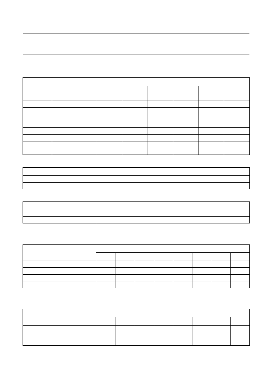
1995 Oct 18
48
Philips Semiconductors
Product specification
One Chip Front-end 1 (OCF1)
SAA7110; SAA7110A
16.4.8
S
UBADDRESS
27 (
DATA BYTE
063 to 056);
GAIN CONTROL ANALOG
#1
Table 44 Static gain control channel 2 (GAI2); data bits D5 to D0
Table 45 Gain mode select (GASL); data bit D6
Table 46 Automatic control integration (HOLD); data bit D7
16.4.9
S
UBADDRESS
28 (
DATA BYTE
071 to 064)
Table 47 White peak control WIPE
16.4.10 S
UBADDRESS
29 (
DATA BYTE
079 to 072)
Table 48 Sync bottom control SBOT
DECIMAL
MULTIPLIER
GAIN
(step size = 0.19 dB)
CONTROL BITS
GAI25
GAI24
GAI23
GAI22
GAI21
GAI20
0
-
2.82 dB
0
0
0
0
0
0
15
0 dB
0
0
1
1
1
1
31
3 dB
0
1
1
1
1
1
47
6 dB
1
0
1
1
1
1
63
9 dB
1
1
1
1
1
1
FUNCTION
CONTROL BIT GASL
Difference value integration
0
Fix value integration
1
FUNCTION
CONTROL BIT HOLD
AGC active
0
AGC integration hold (freeze)
1
DECIMAL WHITE PEAK LEVEL
CONTROL BITS
WIPE7
WIPE6
WIPE5
WIPE4
WIPE3
WIPE2
WIPE1
WIPE0
128
1
0
0
0
0
0
0
0
254
1
1
1
1
1
1
1
0
255 (white peak control off)
1
1
1
1
1
1
1
1
DECIMAL SYNC BOTTOM LEVEL
CONTROL BITS
SBOT7
SBOT6
SBOT5
SBOT4
SBOT3
SBOT2
SBOT1
SBOT0
1
0
0
0
0
0
0
0
1
254
1
1
1
1
1
1
1
0

1995 Oct 18
49
Philips Semiconductors
Product specification
One Chip Front-end 1 (OCF1)
SAA7110; SAA7110A
16.4.11 S
UBADDRESS
2A (
DATA BYTE
087 to 080);
GAIN CONTROL ANALOG
#2
Table 49 Static gain control channel 3 (GAI3); data bits D5 to D0
Table 50 Integration factor white peak (IWIP); data bits D7 and D6
16.4.12 S
UBADDRESS
2B (
DATA BYTE
095 to 088);
GAIN CONTROL ANALOG
#3
Table 51 Static gain control channel 4 (GAI4); data bits D5 to D0
Table 52 Integration factor normal gain (IGAI); data bits D7 and D6
DECIMAL MULTIPLIER
GAIN
(step size = 0.19 dB)
CONTROL BITS
GAI35
GAI34
GAI33
GAI32
GAI31
GAI30
0
-
2.82 dB
0
0
0
0
0
0
15
0 dB
0
0
1
1
1
1
31
3 dB
0
1
1
1
1
1
47
6 dB
1
0
1
1
1
1
63
9 dB
1
1
1
1
1
1
FUNCTION
CONTROL BITS
Fast selection
IWIP1 = 0; IWIP0 = 0
|
IWIP1 = 0; IWIP0 = 1
|
IWIP1 = 1; IWIP0 = 0
Slow selection
IWIP1 = 1; IWIP0 = 1
DECIMAL MULTIPLIER
GAIN
(step size = 0.19 dB)
CONTROL BITS
GAI45
GAI44
GAI43
GAI42
GAI41
GAI40
0
-
2.82 dB
0
0
0
0
0
0
15
0 dB
0
0
1
1
1
1
31
3 dB
0
1
1
1
1
1
47
6 dB
1
0
1
1
1
1
63
9 dB
1
1
1
1
1
1
FUNCTION
CONTROL BITS
Slow selection
IGAI1 = 0; IGAI0 = 0
|
IGAI1 = 0; IGAI0 = 1
|
IGAI1 = 1; IGAI0 = 0
Fast selection
IGAI1 = 1; IGAI0 = 1
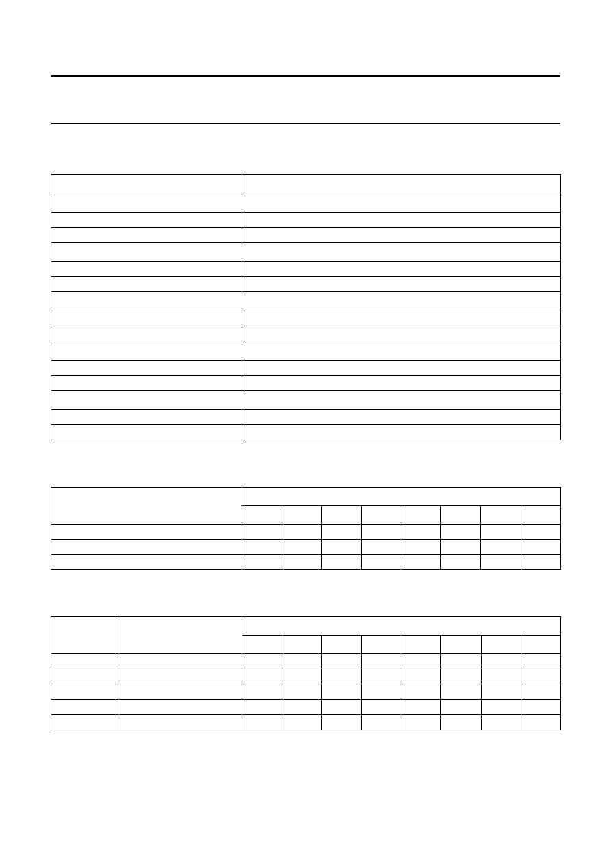
1995 Oct 18
50
Philips Semiconductors
Product specification
One Chip Front-end 1 (OCF1)
SAA7110; SAA7110A
16.4.13 S
UBADDRESS
2C (
DATA BYTE
103 to 096)
Table 53 Mixer control #2
16.4.14 S
UBADDRESS
2D (
DATA BYTE
111 to 104)
Table 54 Integration value gain (IVAL)
16.4.15 S
UBADDRESS
2E (
DATA BYTE
119 to 112)
Table 55 Blanking pulse VBLK-set (VBPS)
Notes
1. Maximum for 60 Hz.
2. Maximum for 50 Hz.
FUNCTION
CONTROL BITS
Two's complement channel 2 (TWO2); data bit D0
Unipolar
TWO2 = 0
Two's complement (normal mode)
TWO2 = 1
Two's complement channel 3 (TWO3); data bit D1
Unipolar
TWO3 = 0
Two's complement (normal mode)
TWO3 = 1
Clamping level select channel 2 (CLS2); data bit D4
CLL21 active
CLS2 = 0
CLL22 active
CLS2 = 1
Clamping level select channel 3 (CLS3); data bit D5
CLL31 active
CLS3 = 0
CLL32 active
CLS3 = 1
Clamping level select channel 4 (CLS4); data bit D7
CLL2n active
CLS4 = 0
CLL3n active
CLS4 = 1
DECIMAL INTEGRATION VALUE GAIN
CONTROL BITS
IVAL7
IVAL6
IVAL5
IVAL4
IVAL3
IVAL2
IVAL1
IVAL0
1
0
0
0
0
0
0
0
1
255
1
1
1
1
1
1
1
1
DECIMAL
MULTIPLIER
SET LINE NUMBER
(step size = 2)
CONTROL BITS
VBPS7 VBPS6 VBPS5 VBPS4 VBPS3 VBPS2 VBPS1 VBPS0
0
0 after rising edge of VS
0
0
0
0
0
0
0
0
131
(1)
262 after rising edge of VS
1
0
0
0
0
0
1
1
156
(2)
312 after rising edge of VS
1
0
0
1
1
1
0
0
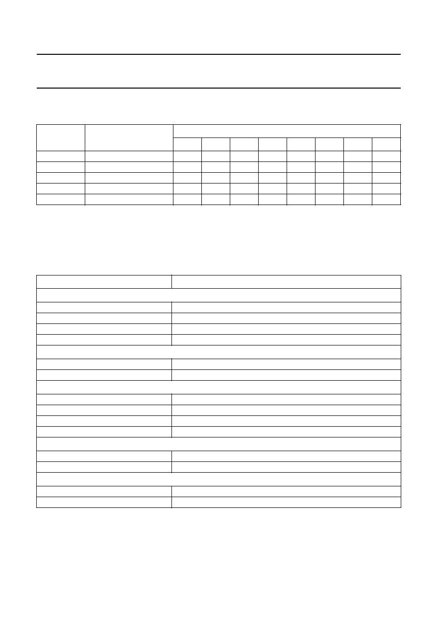
1995 Oct 18
51
Philips Semiconductors
Product specification
One Chip Front-end 1 (OCF1)
SAA7110; SAA7110A
16.4.16 S
UBADDRESS
2F (
DATA BYTE
127 to 120)
Table 56 Blanking pulse VBLK-reset (VBPR)
Notes
1. Maximum for 60 Hz.
2. Maximum for 50 Hz.
16.4.17 S
UBADDRESS
30 (
DATA BYTE
135 to 128)
Table 57 ADCs gain control
DECIMAL
MULTIPLIER
RESET LINE NUMBER
(step size = 2)
CONTROL BITS
VBPR7 VBPR6 VBPR5 VBPR4 VBPR3 VBPR2 VBPR1 VBPR0
0
0 after rising edge of VS
0
0
0
0
0
0
0
0
131
(1)
262 after rising edge of VS
1
0
0
0
0
0
1
1
156
(2)
312 after rising edge of VS
1
0
0
1
1
1
0
0
FUNCTION
CONTROL BITS
Fix gain ADC channel 2 (GAD2); data bits D1 and D0
0 dB
GAD21 = 0; GAD20 = 0
0.05 dB
GAD21 = 0; GAD20 = 1
0.10 dB
GAD21 = 1; GAD20 = 0
0.15 dB
GAD21 = 1; GAD20 = 1
Gain ADC select channel 2 (GAS2); data bit D2
Fix gain via I
2
C-bus GAD2
GAS2 = 0
Automatic gain via loop
GAS2 = 1
Fix gain ADC channel 3 (GAD3); data bits D4 and D3
0 dB
GAD31 = 0; GAD30 = 0
0.05 dB
GAD31 = 0; GAD30 = 1
0.10 dB
GAD31 = 1; GAD30 = 0
0.15 dB
GAD31 = 1; GAD30 = 1
Gain ADC select channel 3 (GAS3); data bit D5
Fix gain via I
2
C-bus GAD3
GAS3 = 0
Automatic gain via loop
GAS3 = 1
White peak mode select (WISL); data bit D6
Difference value integration
WISL = 0
Fix value integration
WISL = 1
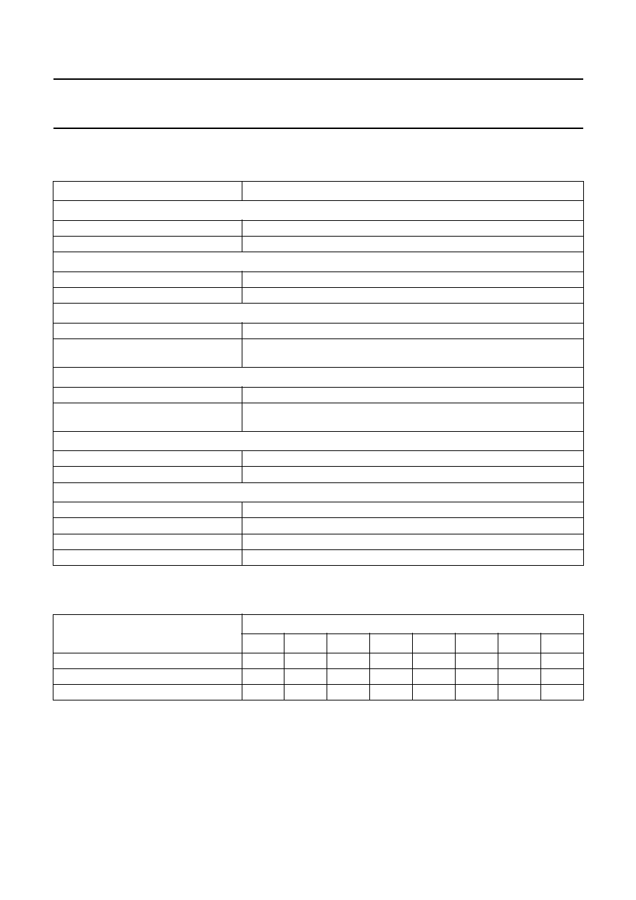
1995 Oct 18
52
Philips Semiconductors
Product specification
One Chip Front-end 1 (OCF1)
SAA7110; SAA7110A
16.4.18 S
UBADDRESS
31 (
DATA BYTE
143 to 136)
Table 58 Mixer control #3
16.4.19 S
UBADDRESS
32 (
DATA BYTE
151 to 144)
Table 59 Integration value white peak (WVAL)
FUNCTION
CONTROL BITS
Pulses I/O control (PULIO); data bit D0
HCL and HSY to input pins
PULIO = 0
HCL and HSY to output pins
PULIO = 1
Pin function switch (VBLKA); data bit D1
GPSW active (normal)
VBLKA = 0
VBLK test output active
VBLKA = 1
DMSD-SQP bypassed (SQPB); data bit D3
DMSD data to YUV output
SQPB = 0
A/D data to YUV output
for test purposes only (do not use)
SQPB = 1
White peak slow up integration enable (WRSE); data bit D4
Hold in white peak mode
WRSE = 0
Slow up integration with 1 value in H or
V (dependent on WIRS)
WRSE = 1
White peak slow up integration select (WIRS); data bit D5
Slow up integration with 1 value per line
WRIS = 0
Slow up integration with 1 value per field
WRIS = 1
Analog test select (AOSL); data bits D7 and D6
AOUT connected to ground
AOSL1 = 0; AOSL0 = 0
AOUT connected to input AD2
AOSL1 = 0; AOSL0 = 0
AOUT connected to input AD3
AOSL1 = 1; AOSL0 = 1
AOUT connected to channel 4
AOSL1 = 1; AOSL0 = 1
DECIMAL INTEGRATION VALUE
WHITE PEAK
CONTROL BITS
WVAL7 WVAL6 WVAL5 WVAL4 WVAL3 WVAL2 WVAL1 WVAL0
1
0
0
0
0
0
0
0
1
127 (max.)
0
1
1
1
1
1
1
1

1995 Oct 18
53
Philips Semiconductors
Product specification
One Chip Front-end 1 (OCF1)
SAA7110; SAA7110A
16.4.20 S
UBADDRESS
33 (
DATA BYTE
159 to 152)
Table 60 Mixer control #4
16.4.21 S
UBADDRESS
34 (
DATA BYTE
167 to 160)
Table 61 Gain update level (GUDL; data bits D5 to D0
Table 62 MUXC phase delay (MUD2); data bits D7 and D6
FUNCTION
CONTROL BITS
Clock select AD2 (CAD2); data bit D2
LLC for test purposes only (do not use)
CAD2 = 0
LLC/2
CAD2 = 1
Clock select AD3 (CAD3); data bit D3
LLC for test purposes only (do not use)
CAD3 = 0
LLC/2
CAD3 = 1
Change sign bit UV data (CHSB); data bit D5
UV output unipolar
CHSB = 0
UV output two's complement
CHSB = 1
Output format select (OFTS); data bit D7
4 : 1 : 1 format
OFTS = 0
4 : 2 : 2 format
OFTS = 1
DECIMAL
HYSTERESIS
FOR 8-BIT GAIN
UPDATE
NEW GAIN - OLD GAIN
CONTROL BITS
GUDL5 GUDL4 GUDL3 GUDL2 GUDL1 GUDL0
0
0 LSB
>0
0
0
0
0
0
0
7
±
7 LSB
>7
0
0
0
1
1
1
>31
off
always
1
X
X
X
X
X
FUNCTION
CONTROL BIT MUD
No phase delay
MUD2 = 0; MUD1 = 0
1 LLC cycle phase delay for CLAA path
MUD2 = 0; MUD1 = 1
2 LLC cycle phase delay for CLAA path
MUD2 = 1; MUD1 = 0
3 LLC cycle phase delay for CLAA path
MUD2 = 1; MUD1 = 1

1995 Oct 18
54
Philips Semiconductors
Product specification
One Chip Front-end 1 (OCF1)
SAA7110; SAA7110A
17 SOURCE SELECTION MANAGEMENT
Table 63 Source selection management examples
INPUT
EXAMPLE 1
EXAMPLE 2
EXAMPLE 3
EXAMPLE 4
SIGNAL
MODE
SIGNAL
MODE
SIGNAL
MODE
SIGNAL
MODE
AIN21
CVBS1
0
CVBS1
0
Y1
6
Y1
6
AIN22
CVBS2
1
C2
7
C2
7
CVBS2
1
AIN31
CVBS3
2
Y2
7
Y2
7
CVBS3
2
AIN32
CVBS4
3
C3
8
C3
8
CVBS4
3
AIN41
CVBS5
4
Y3
8
Y3
8
CVBS5
4
AIN42
CVBS6
5
CVBS6
5
C1
6
C1
6
l
l pagewidth
GAIN4
AAF4
GAIN3
AAF3
GAIN2
AAF2
ADC3
ADC2
AINS4
CSEL
CHRS v BYPS
CLL32
CLL31
CLL22
CLL21
CHROMA
LUMA
YSEL
AINS3
CLS4
AIND4
AIND3
AIND2
AINS2
CLAMP
CON3
CLAMP
CON2
GAIN
CON
GAI4
clamp up/down
clamp up/down
GAI3
GAI2
REF128
REFS2
REFS3
REFS4
AI22
AI21
AI32
AI31
AI42
AI41
CLAMP
CLAMP
CLAMP
GACO
MX340
MX341
MX240
MX241
CLS3
CLS2
MGC839
Fig.20 Source selection overview.
All switch control bits set to LOW.
Fig.21 Mode 0; CVBS1.
handbook, full pagewidth
AI41
AI42
AI31
AI32
AI21
AI22
MGC840
CHROMA
LUMA
AD3
AD2

1995 Oct 18
55
Philips Semiconductors
Product specification
One Chip Front-end 1 (OCF1)
SAA7110; SAA7110A
Fig.22 Mode 1; CVBS2.
handbook, full pagewidth
AI41
AI42
AI31
AI32
AI21
AI22
MGC841
CHROMA
LUMA
AD3
AD2
Fig.23 Mode 2; CVBS3.
handbook, full pagewidth
AI41
AI42
AI31
AI32
AI21
AI22
MGC842
CHROMA
LUMA
AD3
AD2
Fig.24 Mode 3; CVBS4.
handbook, full pagewidth
AI41
AI42
AI31
AI32
AI21
AI22
MGC843
CHROMA
LUMA
AD3
AD2
Fig.25 Mode 4; CVBS5.
handbook, full pagewidth
AI41
AI42
AI31
AI32
AI21
AI22
MGC844
CHROMA
LUMA
AD3
AD2

1995 Oct 18
56
Philips Semiconductors
Product specification
One Chip Front-end 1 (OCF1)
SAA7110; SAA7110A
Fig.26 Mode 5; CVBS6.
handbook, full pagewidth
AI41
AI42
AI31
AI32
AI21
AI22
MGC845
CHROMA
LUMA
AD3
AD2
Fig.27 Mode 6; Y1 + C1.
handbook, full pagewidth
AI41
AI42
AI31
AI32
AI21
AI22
MGC846
CHROMA
LUMA
AD3
AD2
Fig.28 Mode 7; Y2 + C2.
handbook, full pagewidth
AI41
AI42
AI31
AI32
AI21
AI22
MGC847
CHROMA
LUMA
AD3
AD2
Fig.29 Mode 8; Y3 + C3.
handbook, full pagewidth
AI41
AI42
AI31
AI32
AI21
AI22
MGC848
CHROMA
LUMA
AD3
AD2

1995 Oct 18
57
Philips Semiconductors
Product specification
One Chip Front-end 1 (OCF1)
SAA7110; SAA7110A
Table 64 I
2
C-bus control
CONTROL
INPUT
(1)
MODE
0
1
2
3
4
5
6
7
8
9
Subaddress 20
AIND4
1
1
1
1
0
0
0
1
0
-
AIND3
1
1
0
0
1
1
1
0
0
-
AIND2
0
0
1
1
1
1
0
0
1
-
FUSE1
1
-
-
-
-
-
-
-
-
-
FUSE0
1
-
-
-
-
-
-
-
-
-
AINS4
X
X
X
X
1
0
0
X
1
-
AINS3
X
X
1
0
X
X
0
1
0
-
AINS2
1
0
X
X
X
X
1
0
X
-
Subaddress 21
VBCO
0
-
-
-
-
-
-
-
-
-
MS34
0
-
-
-
-
-
-
-
-
-
MX241
0
0
X
X
X
X
0
0
1
-
MX240
0
0
X
X
X
X
0
0
1
-
MS24
0
-
-
-
-
-
-
-
-
-
REFS4
1
1
1
1
0
0
0
1
0
-
REFS3
1
1
0
0
1
1
1
0
0
-
REFS2
0
0
1
1
1
1
0
0
1
-
Subaddress 22
GACO1
0
0
1
1
1
1
0
1
1
-
GACO0
1
1
0
0
1
1
1
0
1
-
CSEL
X
X
X
X
X
X
0
1
0
-
YSEL
0
0
1
1
1
1
0
1
0
-
MUYC
0
-
-
-
-
-
-
-
-
0
CLTS
0
-
-
-
-
-
-
-
-
0
MX341
X
X
0
0
1
1
1
0
0
-
MX340
X
X
1
1
0
0
0
1
1
-
Subaddress 2C
CLS4
X
X
X
X
1
1
1
X
0
-
GABL
0
-
-
-
-
-
-
-
-
-
CLS3
X
X
0
0
0
0
1
0
1
-
CLS2
0
0
X
X
X
X
0
1
X
-
4LSB
0011
-
-
-
-
-
-
-
-
0011
BYPS
0
0
0
0
0
0
1
1
1
-
Subaddresses SU
20H
D9H
D8H
BAH
B8H
7CH
78H
59H
9AH
3CH
-
21H
16H
16H
05H
05H
03H
03H
12H
14H
21H
-
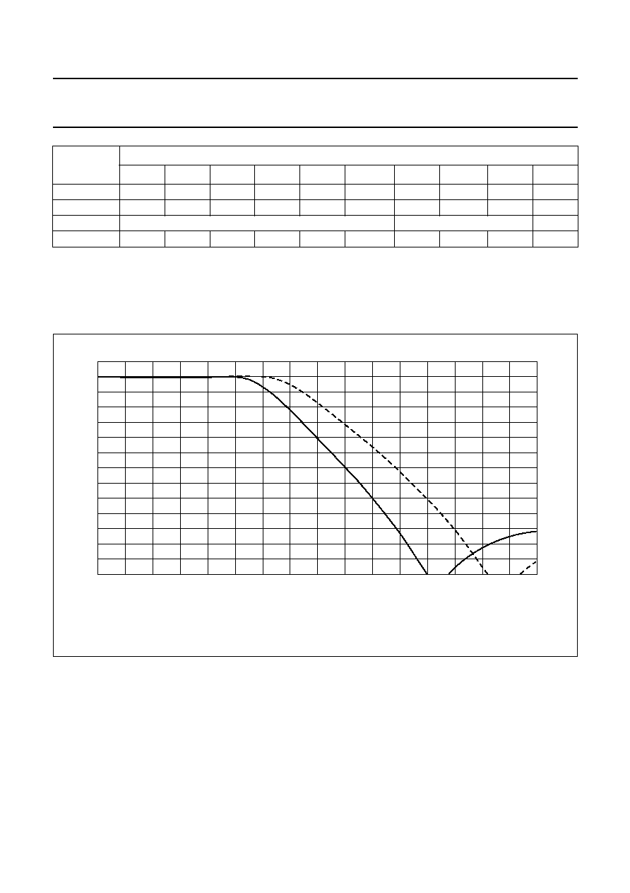
1995 Oct 18
58
Philips Semiconductors
Product specification
One Chip Front-end 1 (OCF1)
SAA7110; SAA7110A
Notes
1. CLL21 = 65d, CLL22 = 128d, CLL31 = 65d, CLL32 = 128d, GAI4 = 15d, GAI3 = 15dGAI2 = 15d; X set 0.
2. Optional: values for AD gain (+2 LSB's gain resolution) active [not active: for all modes 40H].
18 ANTI-ALIAS FILTER GRAPHS
22H
40H
40H
91H
91H
D2H
D2H
42H
B1H
C1H
-
2CH
03H
03H
03H
03H
83H
83H
A3H
13H
23H
-
06H
0XXXXXXX
1XXXXXXX
-
30H
(2)
44H
44H
60H
60H
60H
60H
44H
60H
44H
-
CONTROL
INPUT
(1)
MODE
0
1
2
3
4
5
6
7
8
9
Fig.30 Anti-alias filter graph for SAA7110A.
(1) 50 Hz.
(2) 60 Hz.
handbook, full pagewidth
+
3
-
39
0
2
4
6
8
10
12
14
16
f (MHz)
MGC849
-
3
-
9
-
15
-
21
-
27
-
33
(1)
(2)
A
(dB)
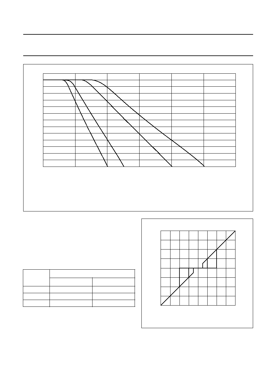
1995 Oct 18
59
Philips Semiconductors
Product specification
One Chip Front-end 1 (OCF1)
SAA7110; SAA7110A
Fig.31 Anti-alias filter graph for SAA7110.
(1) 50 HZ, AFCCS = 0, LLC = 29.50 MHz.
(2) 50 HZ, AFCCS = 1, LLC = 29.50 MHz.
(3) 60 HZ, AFCCS = 0, LLC = 24.54 MHz.
(3) 60 HZ, AFCCS = 1, LLC = 24.54 MHz.
handbook, full pagewidth
+
3
-
39
0
5
10
15
20
25
30
f (MHz)
MGC850
-
3
-
9
-
15
-
21
-
27
-
33
(4)
(1)
(3)
(2)
A
(dB)
19 CORING FUNCTION
19.1
Coring function adjustment by subaddress 06H
to affect band filter output adjustment
The thresholds are related to the 13-bit word width in the
luminance processing part and influence the 1 to 3 LSB
(Yo to Y2) with respect to the 8-bit luminance output.
Table 65 CORI control settings a, b and c of Fig.32
CONTROL BITS
CORI1
CORI0
a
0
1
b
1
0
c
1
1
Fig.32 Coring function.
handbook, halfpage
-
64
-
32
0
+
64
+
64
+
32
-
32
-
64
0
MGC851
+
32
a
b
c
c
b
a

1995 Oct 18
60
Philips Semiconductors
Product specification
One Chip Front-end 1 (OCF1)
SAA7110; SAA7110A
20 LUMINANCE FILTER GRAPHS
Fig.33 Luminance control: SU06H, 50 Hz/CVBS mode, prefilter on and coring off (40 to 63H).
handbook, full pagewidth
8
f
Y (MHz)
18
-
30
0
2
4
6
MGC852
6
VY
(dB)
-
18
-
6
63H
73H
53H
43H
40H
43H
53H
73H
63H
40H
Fig.34 Luminance control: SU06H, 50 Hz/CVBS mode, prefilter on and coring off (40 to 43H).
handbook, full pagewidth
8
f
Y (MHz)
18
-
30
0
2
4
6
MGC853
6
VY
(dB)
-
18
-
6
43H
42H
41H
40H
43H
42H
41H
40H
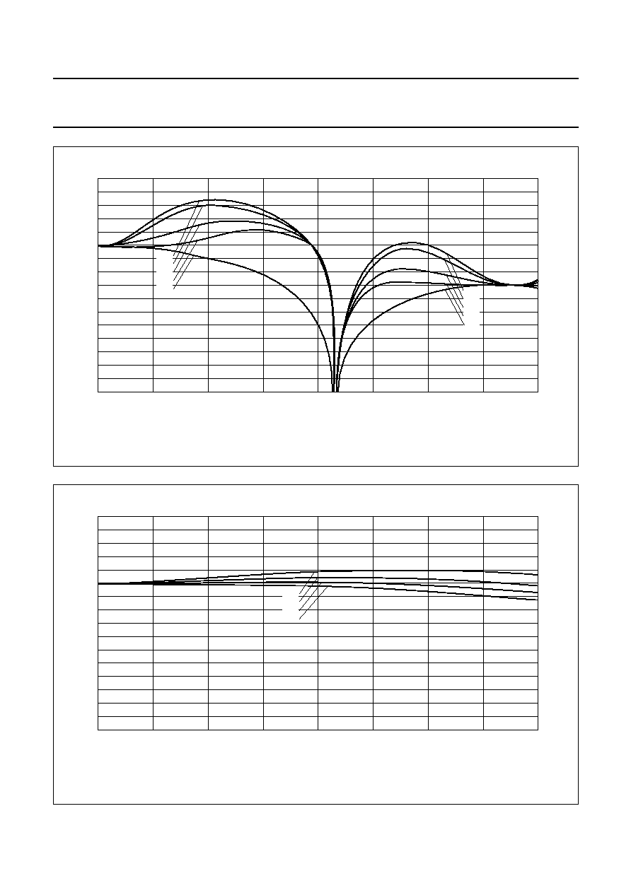
1995 Oct 18
61
Philips Semiconductors
Product specification
One Chip Front-end 1 (OCF1)
SAA7110; SAA7110A
Fig.35 Luminance control: SU06H, 50 Hz/CVBS mode, prefilter off and coring off.
handbook, full pagewidth
8
f
Y (MHz)
18
-
30
0
2
4
6
MGC854
6
VY
(dB)
-
18
-
6
23H
33H
13H
03H
00H
03H
13H
33H
23H
00H
Fig.36 Luminance control: SU06H, 50 Hz/Y + C mode, prefilter off and coring off.
handbook, full pagewidth
8
18
-
30
0
2
4
6
MGC855
6
VY
(dB)
-
18
-
6
83H
82H
81H
80H
f
Y (MHz)
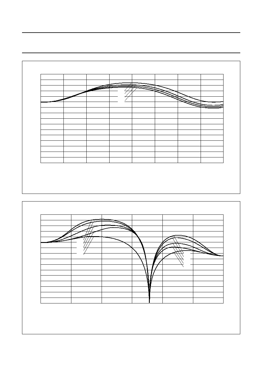
1995 Oct 18
62
Philips Semiconductors
Product specification
One Chip Front-end 1 (OCF1)
SAA7110; SAA7110A
Fig.37 Luminance control: SU06H, 50 Hz/Y + C mode, prefilter on and coring off.
handbook, full pagewidth
8
18
-
30
0
2
4
6
MGC856
6
VY
(dB)
-
18
-
6
C3H
C2H
C1H
C0H
f
Y (MHz)
Fig.38 Luminance control: SU06H, 60 Hz/CVBS mode, prefilter on and coring off.
handbook, full pagewidth
f
Y (MHz)
18
-
30
0
2
4
6
MGC857
6
VY
(dB)
-
18
-
6
63H
73H
53H
43H
40H
43H
53H
73H
63H
40H

1995 Oct 18
63
Philips Semiconductors
Product specification
One Chip Front-end 1 (OCF1)
SAA7110; SAA7110A
Fig.39 Luminance control: SU06H, 60 Hz/CVBS mode, prefilter on and coring off.
handbook, full pagewidth
f
Y (MHz)
18
-
30
0
2
4
6
MGC858
6
VY
(dB)
-
18
-
6
43H
42H
41H
40H
43H
42H
41H
40H
Fig.40 Luminance control: SU06H, 60 Hz/CVBS mode, prefilter off and coring off.
handbook, full pagewidth
f
Y (MHz)
18
-
30
0
2
4
6
MGC859
6
VY
(dB)
-
18
-
6
23H
33H
13H
03H
00H
03H
13H
33H
23H
00H
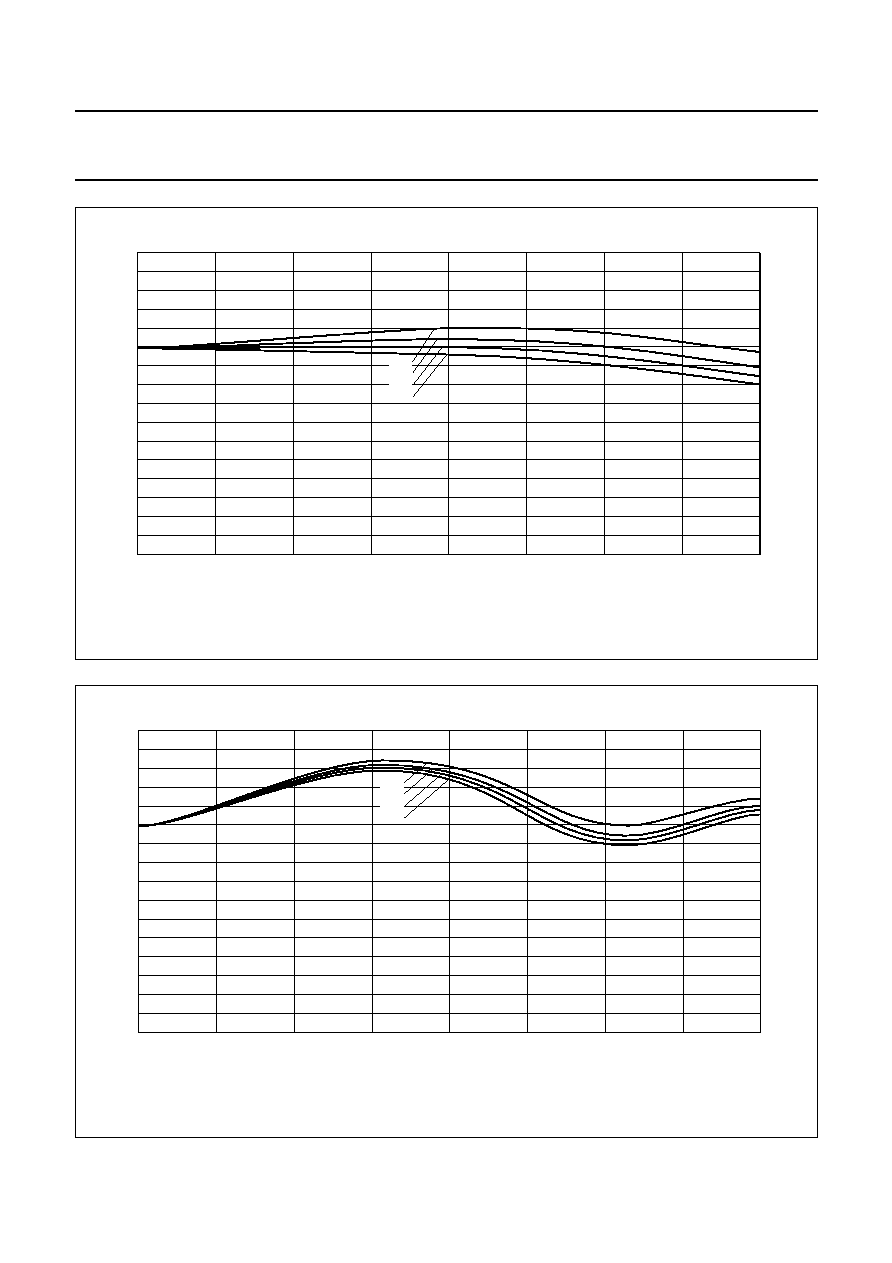
1995 Oct 18
64
Philips Semiconductors
Product specification
One Chip Front-end 1 (OCF1)
SAA7110; SAA7110A
Fig.41 Luminance control: SU06H, 60 Hz/Y + C mode, prefilter off and coring off.
handbook, full pagewidth
8
18
-
30
0
2
4
6
MGC860
6
VY
(dB)
-
18
-
6
83H
82H
81H
80H
f
Y (MHz)
Fig.42 Luminance control: SU06H, 60 Hz/Y + C mode, prefilter on and coring off.
handbook, full pagewidth
8
f
Y
(MHz)
18
-
30
0
2
4
6
MGC861
6
VY
(dB)
-
18
-
6
C3H
C2H
C1H
C0H
1995 Oct 18
65
Philips Semiconductors
Product specification
One Chip Front-end 1 (OCF1)
SAA7110; SAA7110A
21 I
2
C-BUS START SET-UP
The values shown in Table 66 are optimized for the EBU colour bar (100% white and 75% chrominance amplitude)
signal. The decoder output signal level fulfils the CCIR 601 specification. The input of 100% colour bar level is possible,
but the signal (white) peak function reduces the digital luminance output. With a different set-up it is possible to proceed
100% colour bar signal without luminance colour bar reduction. The method is to modify the AD input range for this input
level by reducing the gain reference value (SBOT > 06h) and adjusting the digital Y output level with contrast and
brightness control.
Table 66 I
2
C-bus start set-up
SU
NAME
FUNCTION
BINARY
HEX
7
6
5
4
3
2
1
0
start
00
IDEL7 to IDEL0
increment delay
0
1
0
0
1
1
0
0
4C
01
HSYB7 to HSYB0
horizontal sync (HSY) begin 50 Hz
0
0
1
1
1
1
0
0
3C
02
HSYS7 to HSYS0
horizontal sync (HSY) stop 50 Hz
0
0
0
0
1
1
0
1
0D
03
HCLB7 to HCLB0
horizontal clamp (HCL) begin 50 Hz
1
1
1
0
1
1
1
1
EF
04
HCLS7 to HCLS0
horizontal clamp (HCL) stop 50 Hz
1
0
1
1
1
1
0
1
BD
05
HPHI7 to HPHI0
horizontal sync after PHI1 50 Hz
1
1
1
1
0
0
0
0
F0
06
BYPS, PREF,
BPSS1 to BPSS0,
CORI1 to CORI0,
APER1 to APER0
luminance control
0
0
0
0
0
0
0
0
00
07
HUEC7 to HUEC0
hue control
0
0
0
0
0
0
0
0
00
08
CKTQ4 to CKTQ0, XXX
colour killer threshold PAL
1
1
1
1
1
X
X
X
F8
09
CKTS4 to CKTS0, XXX
colour killer threshold SECAM
1
1
1
1
1
X
X
X
F8
0A
PLSE7 to PLSE0
PAL switch sensitivity
0
1
1
0
0
0
0
0
60
0B
SESE7 to SESE0
SECAM switch sensitivity
0
1
1
0
0
0
0
0
5B
0C
COLO, LFIS1 to LFIS0,
XXXXX
gain control chrominance
0
0
0
X
X
X
X
X
00
0D
VTRC, XXX, RTSE, HRMV,
SSTB, SECS
standard/mode control
0
X
X
X
0
1
1
0
06
0E
HPLL, XX, OEHV, OEYC,
CHRS, X, GPSW
I/O and clock control
0
X
X
1
1
0
X
0
18
0F
AUFD, FSEL, SXCR, SCEN,
X, YDEL2 to YDEL0
control #1
1
0
0
1
X
0
0
0
90
10
XXXXX, HRFS,
VNOI1 to VNOI0
control #2
X
X
X
X
X
0
0
0
00
11
CHCV7 to CHCV0 PAL
chrominance gain reference
0
1
0
1
1
0
0
1
59
CHCV7 to CHCV0 NTSC
0
0
1
0
1
1
0
0
2C
12
SATN7 to SATN0
chrominance saturation
0
1
0
0
0
0
0
0
40
13
CONT7 to CONT0
luminance contrast
0
1
0
0
0
1
1
0
46
14
HS6B7 to HS6B70
horizontal sync (HSY) begin 60 Hz
0
1
0
0
0
0
1
0
42
15
HS6S7 to HS6S0
horizontal sync (HSY) stop 60 Hz
0
0
0
1
1
0
1
0
1A
16
HC6B7 to HC6B0
horizontal clamp (HCL) begin 60 Hz
1
1
1
1
1
1
1
1
FF
17
HC6S7 to HC6S0
horizontal clamp (HCL) stop 60 Hz
1
1
0
1
1
0
1
0
DA
18
HP6I7 to HP6I0
horizontal sync after PHI1 60 Hz
1
1
1
1
0
0
0
0
F0
19
BRIGI7 to BRIG0
luminance brightness
1
0
0
0
1
0
1
1
8B
1995 Oct 18
66
Philips Semiconductors
Product specification
One Chip Front-end 1 (OCF1)
SAA7110; SAA7110A
21.1
Remarks to Table 66
Values recommended for a CVBS (PAL or NTSC) signal, input AI21 via A/D channel 2 (MODE 0), and 4 : 2 : 2 CCIR
output signal level; all X values must be set LOW, X* value is don't care; HPHI and HP6I are application dependent.
1A-1F reserved
20
AIND4, AIND3, AIND2,
FUSE1 to FUSE0, AINS4,
AINS3, AINS2
analog control #1
1
1
0
1
1
0
0
1
D9
21
VBCO, MS34,
MX241 to MX240, MS24,
REFS4, REFS3, REFS2
analog control #2
0
0
0
1
0
1
1
0
16
22
GACO1 to GACO0, CSEL,
YSEL, MUYC, CLTS,
MX341 to MX340
mixer control #1
0
1
0
0
0
0
0
0
40
23
CLL217 to CLL210
clamping level control channel 21
0
1
0
0
0
0
0
1
41
24
CLL227 to CLL220
clamping level control channel 22
1
0
0
0
0
0
0
0
80
25
CLL317 to CLL310
clamping level control channel 31
0
1
0
0
0
0
0
1
41
26
CLL327 to CLL320
clamping level control channel 32
1
0
0
0
0
0
0
0
80
27
HOLD, GASL,
GAI25 to GAI20
gain control analog #1
0
1
0
0
1
1
1
1
4F
28
WIPE7 to WIPE0
white peak control
1
1
1
1
1
1
1
0
FE
29
SBOT7 to SBOT0
sync bottom control
0
0
0
0
0
0
0
1
01
2A
IWIP1 to IWIP0,
GAI35 to GAI30
gain control analog #2
1
1
0
0
1
1
1
1
CF
2B
IGAI1 to IGAI0,
GAI45 to GAI40
gain control analog #3
0
0
0
0
1
1
1
1
0F
2C
CLS4, X, CLS3, CLS2,
TWO3, TWO2
mixer control #2
0
X
0
0
X
X
1
1
03
2D
IVAL7 to IVAL0
integration value gain
0
0
0
0
0
0
0
1
01
2E
VBPS7 to VBPS0; 50 Hz
vertical blanking pulse SET
1
0
0
1
1
0
1
0
9A
VBPS7 to VBPS0; 60 Hz
1
0
0
0
0
0
0
1
81
2F
VBPR7 to VBPR0; 50 Hz
vertical blanking pulse RESET
0
0
0
0
0
0
1
1
03
VBPR7 to VBPR0; 60 Hz
0
0
0
0
0
0
1
1
30
X, WISL, GAS3,
GAD31 to GAD30, GAS2,
GAD21 to GAD20
ADCs gain control
X
1
0
0
0
0
0
0
44
31
AOSL1 to AOSL0, WIRS,
WRSE, SQPB, X, VBLKA,
PULIO
mixer control #3
0
1
1
1
0
X*
0
1
71
32
WVAL7 to WVAL0
integration value white peak
0
0
0
0
0
0
1
0
02
33
OFTS, X, CHSB, X, CAD3,
CAD2, XX
mixer control #4
1
X
0
X
1
1
X
X
8C
34
MUD2, MUD1,
GUDL5 to GUDL0
gain update level
0
0
0
0
0
0
1
1
03
SU
NAME
FUNCTION
BINARY
HEX
7
6
5
4
3
2
1
0
start

1995 Oct 18
67
Philips Semiconductors
Product specification
One Chip Front-end 1 (OCF1)
SAA7110; SAA7110A
22 APPLICATION INFORMATION
handbook, full pagewidth
Q1(26.8 MHz)
Y7 to Y0
SCL
V
DD
AI32
FEIN (MUXC)
SDA
CGCE
AOUT
RTCO
VS
LLC
ODD (VL)
PLIN (HL)
GPSW (VBLK)
LFCO
RESET
CREF
LLC2
HREF
V
SS
V
SSA
V
DDA
V
SSA
V
DD
V
SS
V
DD1
V
DD2
V
DD3
V
DD4
V
DD5
V
SS
HS
Y7
Y6
Y5
Y4
Y3
Y2
Y1
Y0
V
SS
SAA7110
SAA7110A
R4
75
C24
10 nF
C7
100 nF
100 nF
100 nF
100 nF
100 nF
100 nF
C8
C9
C11
C12
C13
C14
C15
R7
1 k
C17
L1
10
µ
H
C16
1 nF
10 pF 10 pF
C18
R8
1 k
27
34
44
52
68
16 12
20
24
45
46
47
48
49
50
53
54
42
41
3
23
29
40
64
39
30
31
32
26
HSY
HCL
36
37
38
9
8
7
4
2
1
28
35
43
51
67
14 10
18
25
22
15
6
5
63
33
66
65
i.c.
i.c.
MGC862
V
SSA
i.c.
100 nF
100 nF
100 nF
C10
AI31
R3
75
C3
10 nF
17
V
SSA
AI42
R6
75
C6
10 nF
11
V
SSA
AI41
R5
75
C5
10 nF
13
V
SSA
AI22
R2
75
C2
10 nF
19
V
SSA
V
SS
AI21
R1
75
C1
10 nF
21
V
SSA
UV7 to UV0
UV7
UV6
UV5
UV4
UV3
UV2
UV1
UV0
55
56
57
58
59
60
61
62
XTALO
XTALI
SA AP SP
Fig.43 Application diagram.
Unused analog inputs should not be connected.
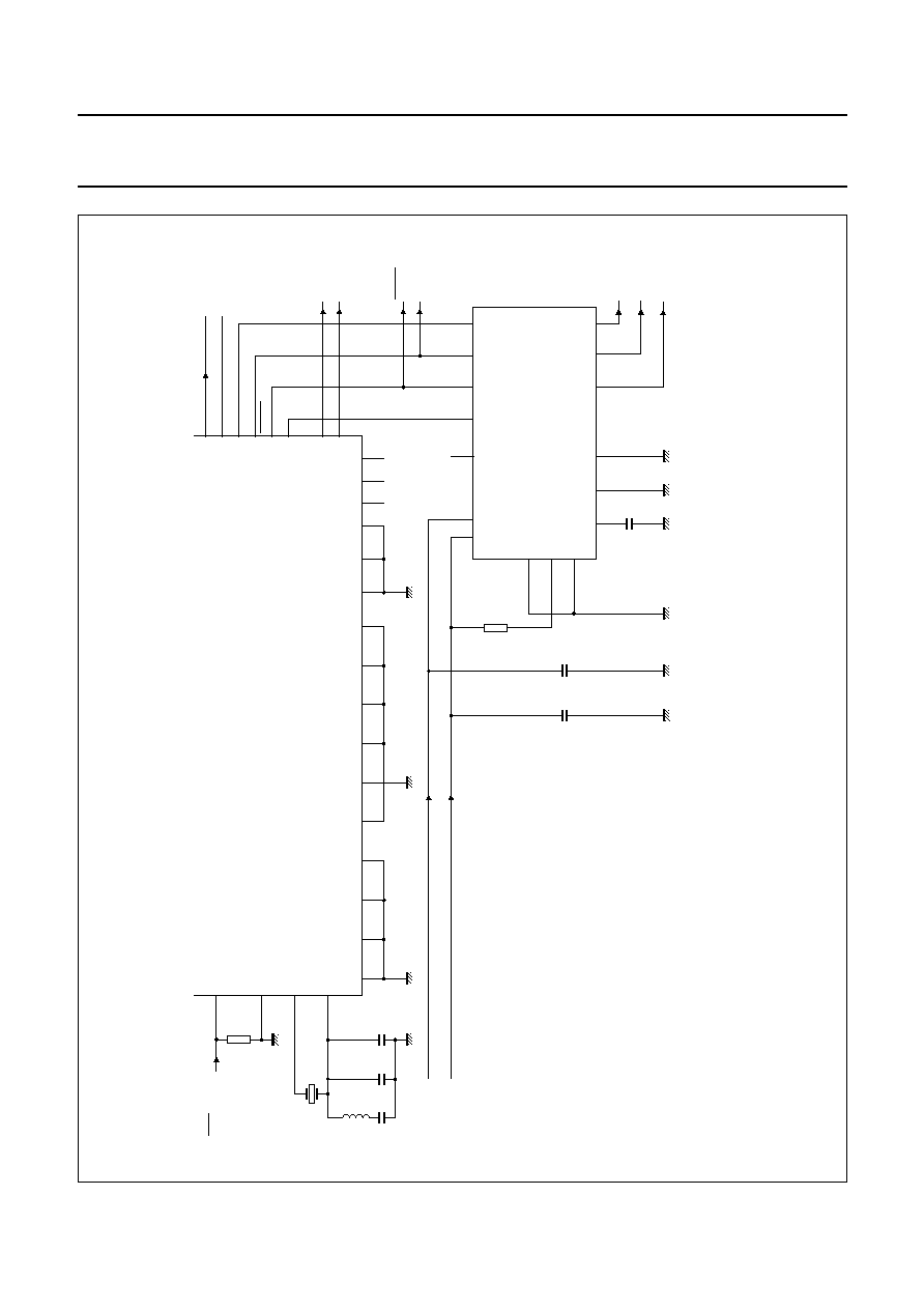
1995
Oct
18
68
Philips Semiconductors
Product specification
One Chip Front-end 1 (OCF1)
SAA71
10; SAA71
10A
This text is here in white to force landscape pages to be rotated correctly when browsing through the pdf in the Acrobat reader.This text is here in
_
white to force landscape pages to be rotated correctly when browsing through the pdf in the Acrobat reader.This text is here inThis text is here in
white to force landscape pages to be rotated correctly when browsing through the pdf in the Acrobat reader. white to force landscape pages to be ...
handbook, full pagewidth
18
25
63
33
65
66
14
22
10
67
51
43
35
28
4
2
1
7
8
9
40
30
29
31
32
26
36
37
RESET
LFCO
CREF
LLC2
LLC
n.c.
i.c.
i.c.
i.c.
HCL
HSY
RESET
CREF
LFCO2 LFCO RESN CREF LLCA
ODD (VL)
VSSA0
VSSA
VSS
VSSA2 VSSA3 VSSA4
VDDA
VDDD
VSS(S)
VSS
VSS
VSS
VSS
VSS
VSS
VSSA
PORD
VSSD
VSS
SA
AP
SP
FEIN (MUXC)
1 k
1 k
R7
CGCE
XTALO
L1
C16
C17
C18
XTALI
(26.8 MHZ)
Q1
1 nF
10
µ
H
10 pF
10 pF
19
8,17 5
11
12
15
7
3
4
6, 9
13, 18
10
20
14
LLC2B
C20
0.1
µ
F
LLC2A
LLCB
MS
1
2
16
CE
R10
C21
C22
100 nF
100 nF
SAA7197
LFCOSEL
MGC863
SAA7110
SAA7110A
Fig.44 Application diagram with external Clock Generator Circuit (CGC).
The OCF1 supports for special applications the use of an external CGC (SAA7197). For normal operation the built-in CGC fulfils all requirements.

1995 Oct 18
69
Philips Semiconductors
Product specification
One Chip Front-end 1 (OCF1)
SAA7110; SAA7110A
23 START-UP, SOURCE SELECT AND STANDARD DETECTION FLOW EXAMPLE
Fig.45 Software flow example.
handbook, full pagewidth
power on
mode 0 set-up
initialization
start source select
REFS active
mode select
REFS off
clamp active
PAL set-up
NTSC set-up
B&W50 set-up
B&W60 set-up
stop
SECAM set-up
standard automatic
?status byte?
precharge clamping capacitor
mode 0 to 7
B&W50? yes
=
XX0XXX00
B&W60? yes
=
XX1XXX00
NTSC? yes
=
XX1XXXXX
SECAM? yes
=
XX0XXX01
B&W50?
B&W60?
NTSC?
no
no
no
SECAM?
no
yes
yes
yes
yes
without standard routine
MGC864

1995 Oct 18
70
Philips Semiconductors
Product specification
One Chip Front-end 1 (OCF1)
SAA7110; SAA7110A
23.1
CODE 0 STARTUP and STANDARD Procedure
SLAVE 9C
!OCF1 NTSC-setup
SUB 00 WRITE
4C 3C 0D EF BD F0 00 00
F8 F8 60 60 00 06 18 90
00 2C 40 46 42 1A FF DA
F0 8B 00 00 00 00 00 00
D9 17 40 41 80 41 80 4F
FE 01 CF 0F 03 01 81 03
44 75 01 8C 03
SUB 21 WRITE 16
!REFS OFF CLAMP AKTIV
READ 1
!Status?
#STANDARD
IF 1 @XX0XXX00
!NO COLOR
THEN GOTO BW_50Hz
ENDIF
IF 1 @XX1XXX00 !NO COLOR
THEN GOTO BW_60Hz
ENDIF
SUB 06 WRITE 00
ENDIF
IF 1 @XX1XXXXX !60Hz
THEN GOTO NTSC
ENDIF
IF 1 @XX0XXXXX !50Hz
THEN GOTO PAL
ENDIF
#BW_50Hz
PRINT "BLACK&WHITE"
SUB 06 WRITE 80
SUB 2E WRITE 9A !VBPS
GOTO STOP
#BW_60Hz
PRINT "BLACK&WHITE"
SUB 06 WRITE 80
SUB 2E WRITE 81 !VBPS
GOTO STOP
#NTSC
SUB 0D WRITE 06 !SECS -> 0
SUB 11 WRITE 2C !CHCV
SUB 2E WRITE 81 !VBPS
PRINT "NTSC"
GOTO STOP
#PAL
SUB 0D WRITE 06 !SECS -> 0
SUB 11 WRITE 59 !CHCV
SUB 2E WRITE 9A !VBPS
PAUSE %150 !150ms
IF 1 @XX0XXX01
THEN GOTO SECAM
ELSE PRINT "PAL"
GOTO STOP
#SECAM
SUB 0D WRITE 07 !SECS -> 1
PRINT "SECAM"
GOTO STOP
#STOP
23.2
MODE 0 Source Select Procedure
SLAVE 9C !OCF1
SUB 06 WRITE 00 !CVBS MODE 0
SUB 20 WRITE D9 !AI21 ACTIVE
SUB 21 WRITE 17 !REFS ON
SUB 22 WRITE 40 !AD2->LUMA and CHROMA
SUB 2C WRITE 03 !CLAMP SELECT
SUB 30 WRITE 44 !Gain AD2 active
SUB 31 WRITE 75 !AOSL -> 01b
SUB 21 WRITE 16 !REFS OFF CLAMP AKTIV
23.3
MODE 1 Source Select Procedure
SLAVE 9C !OCF1
SUB 06 WRITE 00 !CVBS MODE 1
SUB 20 WRITE D8 !AI22 ACTIVE
SUB 21 WRITE 17 !REFS ON
SUB 22 WRITE 40 !AD2->LUMA and CHROMA
SUB 2C WRITE 03 !CLAMP SELECT
SUB 30 WRITE 44 !Gain AD2 active
SUB 31 WRITE 75 !AOSL -> 01b
SUB 21 WRITE 16 !REFS OFF CLAMP AKTIV
23.4
MODE 2 Source Select Procedure
SLAVE 9C !OCF1
SUB 06 WRITE 00 !CVBS MODE 2
SUB 20 WRITE BA !AI31 ACTIVE
SUB 21 WRITE 07 !REFS ON
SUB 22 WRITE 91 !AD3->LUMA and CHROMA
SUB 2C WRITE 03 !CLAMP SELECT
SUB 30 WRITE 60 !Gain AD3 active
SUB 31 WRITE B5 !AOSL -> 10b
SUB 21 WRITE 05 !REFS OFF CLAMP AKTIV
23.5
MODE 3 Source Select Procedure
SLAVE 9C !OCF1
SUB 06 WRITE 00 !CVBS MODE 3
SUB 20 WRITE B8 !AI32 ACTIVE
SUB 21 WRITE 07 !REFS ON
SUB 22 WRITE 91 !AD3->LUMA and CHROMA
SUB 2C WRITE 03 !CLAMP SELECT
SUB 30 WRITE 60 !Gain AD3 active
SUB 31 WRITE B5 !AOSL -> 10b
SUB 21 WRITE 05 !REFS OFF CLAMP AKTIV

1995 Oct 18
71
Philips Semiconductors
Product specification
One Chip Front-end 1 (OCF1)
SAA7110; SAA7110A
23.6
MODE 4 Source Select Procedure
SLAVE 9C !OCF1
SUB 06 WRITE 00 !CVBS MODE 4
SUB 20 WRITE 7C !AI41 ACTIVE
SUB 21 WRITE 07 !REFS ON
SUB 22 WRITE D2 !AD3->LUMA and CHROMA
SUB 2C WRITE 83 !CLAMP SELECT
SUB 30 WRITE 60 !Gain AD3 active
SUB 31 WRITE B5 !AOSL -> 10b
SUB 21 WRITE 03 !REFS OFF CLAMP AKTIV
23.7
MODE 5 Source Select Procedure
SLAVE 9C !OCF1
SUB 06 WRITE 00 !CVBS MODE 5
SUB 20 WRITE 78 !AI41 ACTIVE
SUB 21 WRITE 07 !REFS ON
SUB 22 WRITE D2 !AD3->LUMA and CHROMA
SUB 2C WRITE 83 !CLAMP SELECT
SUB 30 WRITE 60 !Gain AD3 active
SUB 31 WRITE B5 !AOSL -> 10b
SUB 21 WRITE 03 !REFS OFF CLAMP AKTIV
23.8
MODE 6 Source Select Procedure
SLAVE 9C !OCF1
SUB 06 WRITE 80 !Y+C MODE 6
SUB 20 WRITE 59 !AI21=Y, AI42=C
SUB 21 WRITE 17 !REFS ON
SUB 22 WRITE 42 !AD2->LUMA, AD3->CHR
SUB 2C WRITE A3 !CLAMP SELECT
SUB 30 WRITE 44 !Gain AD2 active
SUB 31 WRITE 75 !AOSL -> 01
SUB 21 WRITE 12 !REFS OFF CLAMP AKTIV
23.9
MODE 7 Source Select Procedure
SLAVE 9C !OCF1
SUB 06 WRITE 80 !Y+C MODE 7
SUB 20 WRITE 9A !AI31=Y, AI22=C
SUB 21 WRITE 17 !REFS ON
SUB 22 WRITE B1 !AD3->LUMA, AD2->CHR
SUB 2C WRITE 13 !CLAMP SELECT
SUB 30 WRITE 60 !Gain AD3 active
SUB 31 WRITE B5 !AOSL -> 10b
SUB 21 WRITE 14 !REFS OFF CLAMP AKTIV
23.10 MODE 8 Source Select Procedure
SLAVE 9C !OCF1
SUB 06 WRITE 80 !Y+C MODE 8
SUB 20 WRITE 3C !AI41=Y, AI32=C
SUB 21 WRITE 27 !REFS ON
SUB 22 WRITE C1 !AD2->LUMA, AD3->CHR
SUB 2C WRITE 23 !CLAMP SELECT
SUB 30 WRITE 44 !Gain AD2 active
SUB 31 WRITE 75 !AOSL -> 01
SUB 21 WRITE 21 !REFS OFF CLAMP AKTIV
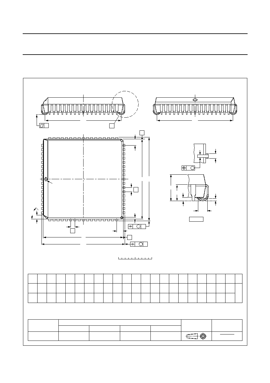
1995 Oct 18
72
Philips Semiconductors
Product specification
One Chip Front-end 1 (OCF1)
SAA7110; SAA7110A
24 PACKAGE OUTLINE
REFERENCES
OUTLINE
VERSION
EUROPEAN
PROJECTION
ISSUE DATE
IEC
JEDEC
EIAJ
Note
1. Plastic or metal protrusions of 0.01 inches maximum per side are not included.
SOT188-2
44
60
68
1
9
10
26
43
27
61
detail X
(A )
3
b
p
w
M
A
1
A
A
4
L
p
b
1
k
1
k
X
y
e
E
B
D
H
E
H
v
M
B
D
Z D
A
Z E
e
v
M
A
pin 1 index
112E10
MO-047AC
0
5
10 mm
scale
92-11-17
95-03-11
PLCC68: plastic leaded chip carrier; 68 leads
SOT188-2
UNIT
A
A
min.
max.
max.
max. max.
1
A
4
b
p
E
(1)
(1)
(1)
e
H
E
Z
y
w
v
mm
4.57
4.19
0.51
3.30
0.53
0.33
0.021
0.013
1.27
0.51
2.16
45
o
0.18
0.10
0.18
DIMENSIONS (millimetre dimensions are derived from the original inch dimensions)
D
(1)
24.33
24.13
H
D
25.27
25.02
E
Z
2.16
D
b
1
0.81
0.66
k
1.22
1.07
k
1
0.180
0.165
0.020
0.13
A
3
0.25
0.01
0.05
0.020
0.085
0.007 0.004
0.007
L
p
1.44
1.02
0.057
0.040
0.958
0.950
24.33
24.13
0.958
0.950
0.995
0.985
25.27
25.02
0.995
0.985
e
E
e
D
23.62
22.61
0.930
0.890
23.62
22.61
0.930
0.890
0.085
0.032
0.026
0.048
0.042
E
e
inches
D
e

1995 Oct 18
73
Philips Semiconductors
Product specification
One Chip Front-end 1 (OCF1)
SAA7110; SAA7110A
25 SOLDERING
25.1
Introduction
There is no soldering method that is ideal for all IC
packages. Wave soldering is often preferred when
through-hole and surface mounted components are mixed
on one printed-circuit board. However, wave soldering is
not always suitable for surface mounted ICs, or for
printed-circuits with high population densities. In these
situations reflow soldering is often used.
This text gives a very brief insight to a complex technology.
A more in-depth account of soldering ICs can be found in
our
"IC Package Databook" (order code 9398 652 90011).
25.2
Reflow soldering
Reflow soldering techniques are suitable for all PLCC
packages.
The choice of heating method may be influenced by larger
PLCC packages (44 leads, or more). If infrared or vapour
phase heating is used and the large packages are not
absolutely dry (less than 0.1% moisture content by
weight), vaporization of the small amount of moisture in
them can cause cracking of the plastic body. For more
information, refer to the Drypack chapter in our
"Quality
Reference Handbook" (order code 9398 510 63011).
Reflow soldering requires solder paste (a suspension of
fine solder particles, flux and binding agent) to be applied
to the printed-circuit board by screen printing, stencilling or
pressure-syringe dispensing before package placement.
Several techniques exist for reflowing; for example,
thermal conduction by heated belt. Dwell times vary
between 50 and 300 seconds depending on heating
method. Typical reflow temperatures range from
215 to 250
∞
C.
Preheating is necessary to dry the paste and evaporate
the binding agent. Preheating duration: 45 minutes at
45
∞
C.
25.3
Wave soldering
Wave soldering techniques can be used for all PLCC
packages if the following conditions are observed:
∑
A double-wave (a turbulent wave with high upward
pressure followed by a smooth laminar wave) soldering
technique should be used.
∑
The longitudinal axis of the package footprint must be
parallel to the solder flow.
∑
The package footprint must incorporate solder thieves at
the downstream corners.
During placement and before soldering, the package must
be fixed with a droplet of adhesive. The adhesive can be
applied by screen printing, pin transfer or syringe
dispensing. The package can be soldered after the
adhesive is cured.
Maximum permissible solder temperature is 260
∞
C, and
maximum duration of package immersion in solder is
10 seconds, if cooled to less than 150
∞
C within
6 seconds. Typical dwell time is 4 seconds at 250
∞
C.
A mildly-activated flux will eliminate the need for removal
of corrosive residues in most applications.
25.4
Repairing soldered joints
Fix the component by first soldering two diagonally-
opposite end leads. Use only a low voltage soldering iron
(less than 24 V) applied to the flat part of the lead. Contact
time must be limited to 10 seconds at up to 300
∞
C. When
using a dedicated tool, all other leads can be soldered in
one operation within 2 to 5 seconds between
270 and 320
∞
C.

1995 Oct 18
74
Philips Semiconductors
Product specification
One Chip Front-end 1 (OCF1)
SAA7110; SAA7110A
26 DEFINITIONS
27 LIFE SUPPORT APPLICATIONS
These products are not designed for use in life support appliances, devices, or systems where malfunction of these
products can reasonably be expected to result in personal injury. Philips customers using or selling these products for
use in such applications do so at their own risk and agree to fully indemnify Philips for any damages resulting from such
improper use or sale.
28 PURCHASE OF PHILIPS I
2
C COMPONENTS
Data sheet status
Objective specification
This data sheet contains target or goal specifications for product development.
Preliminary specification
This data sheet contains preliminary data; supplementary data may be published later.
Product specification
This data sheet contains final product specifications.
Limiting values
Limiting values given are in accordance with the Absolute Maximum Rating System (IEC 134). Stress above one or
more of the limiting values may cause permanent damage to the device. These are stress ratings only and operation
of the device at these or at any other conditions above those given in the Characteristics sections of the specification
is not implied. Exposure to limiting values for extended periods may affect device reliability.
Application information
Where application information is given, it is advisory and does not form part of the specification.
Purchase of Philips I
2
C components conveys a license under the Philips' I
2
C patent to use the
components in the I
2
C system provided the system conforms to the I
2
C specification defined by
Philips. This specification can be ordered using the code 9398 393 40011.

1995 Oct 18
75
Philips Semiconductors
Product specification
One Chip Front-end 1 (OCF1)
SAA7110; SAA7110A
NOTES

Philips Semiconductors ≠ a worldwide company
Argentina: IEROD, Av. Juramento 1992 - 14.b, (1428)
BUENOS AIRES, Tel. (541)786 7633, Fax. (541)786 9367
Australia: 34 Waterloo Road, NORTH RYDE, NSW 2113,
Tel. (02)805 4455, Fax. (02)805 4466
Austria: Triester Str. 64, A-1101 WIEN, P.O. Box 213,
Tel. (01)60 101-1236, Fax. (01)60 101-1211
Belgium: Postbus 90050, 5600 PB EINDHOVEN, The Netherlands,
Tel. (31)40-2783749, Fax. (31)40-2788399
Brazil: Rua do Rocio 220 - 5
th
floor, Suite 51,
CEP: 04552-903-S√O PAULO-SP, Brazil.
P.O. Box 7383 (01064-970),
Tel. (011)821-2333, Fax. (011)829-1849
Canada: PHILIPS SEMICONDUCTORS/COMPONENTS:
Tel. (800) 234-7381, Fax. (708) 296-8556
Chile: Av. Santa Maria 0760, SANTIAGO,
Tel. (02)773 816, Fax. (02)777 6730
China/Hong Kong: 501 Hong Kong Industrial Technology Centre,
72 Tat Chee Avenue, Kowloon Tong, HONG KONG,
Tel. (852)2319 7888, Fax. (852)2319 7700
Colombia: IPRELENSO LTDA, Carrera 21 No. 56-17,
77621 BOGOTA, Tel. (571)249 7624/(571)217 4609,
Fax. (571)217 4549
Denmark: Prags Boulevard 80, PB 1919, DK-2300
COPENHAGEN S, Tel. (032)88 2636, Fax. (031)57 1949
Finland: Sinikalliontie 3, FIN-02630 ESPOO,
Tel. (358)0-615 800, Fax. (358)0-61580 920
France: 4 Rue du Port-aux-Vins, BP317,
92156 SURESNES Cedex,
Tel. (01)4099 6161, Fax. (01)4099 6427
Germany: P.O. Box 10 63 23, 20043 HAMBURG,
Tel. (040)3296-0, Fax. (040)3296 213.
Greece: No. 15, 25th March Street, GR 17778 TAVROS,
Tel. (01)4894 339/4894 911, Fax. (01)4814 240
India: Philips INDIA Ltd, Shivsagar Estate, A Block,
Dr. Annie Besant Rd. Worli, Bombay 400 018
Tel. (022)4938 541, Fax. (022)4938 722
Indonesia: Philips House, Jalan H.R. Rasuna Said Kav. 3-4,
P.O. Box 4252, JAKARTA 12950,
Tel. (021)5201 122, Fax. (021)5205 189
Ireland: Newstead, Clonskeagh, DUBLIN 14,
Tel. (01)7640 000, Fax. (01)7640 200
Italy: PHILIPS SEMICONDUCTORS S.r.l.,
Piazza IV Novembre 3, 20124 MILANO,
Tel. (0039)2 6752 2531, Fax. (0039)2 6752 2557
Japan: Philips Bldg 13-37, Kohnan 2 -chome, Minato-ku, TOKYO 108,
Tel. (03)3740 5130, Fax. (03)3740 5077
Korea: Philips House, 260-199 Itaewon-dong,
Yongsan-ku, SEOUL, Tel. (02)709-1412, Fax. (02)709-1415
Malaysia: No. 76 Jalan Universiti, 46200 PETALING JAYA,
SELANGOR, Tel. (03)750 5214, Fax. (03)757 4880
Mexico: 5900 Gateway East, Suite 200, EL PASO, TX 79905,
Tel. 9-5(800)234-7381, Fax. (708)296-8556
Netherlands: Postbus 90050, 5600 PB EINDHOVEN, Bldg. VB,
Tel. (040)2783749, Fax. (040)2788399
New Zealand: 2 Wagener Place, C.P.O. Box 1041, AUCKLAND,
Tel. (09)849-4160, Fax. (09)849-7811
Norway: Box 1, Manglerud 0612, OSLO,
Tel. (022)74 8000, Fax. (022)74 8341
Pakistan: Philips Electrical Industries of Pakistan Ltd.,
Exchange Bldg. ST-2/A, Block 9, KDA Scheme 5, Clifton,
KARACHI 75600, Tel. (021)587 4641-49,
Fax. (021)577035/5874546
Philippines: PHILIPS SEMICONDUCTORS PHILIPPINES Inc,
106 Valero St. Salcedo Village, P.O. Box 2108 MCC, MAKATI,
Metro MANILA, Tel. (63) 2 816 6380, Fax. (63) 2 817 3474
Portugal: PHILIPS PORTUGUESA, S.A.,
Rua dr. AntÛnio Loureiro Borges 5, Arquiparque - Miraflores,
Apartado 300, 2795 LINDA-A-VELHA,
Tel. (01)4163160/4163333, Fax. (01)4163174/4163366
Singapore: Lorong 1, Toa Payoh, SINGAPORE 1231,
Tel. (65)350 2000, Fax. (65)251 6500
South Africa: S.A. PHILIPS Pty Ltd.,
195-215 Main Road Martindale, 2092 JOHANNESBURG,
P.O. Box 7430, Johannesburg 2000,
Tel. (011)470-5911, Fax. (011)470-5494
Spain: Balmes 22, 08007 BARCELONA,
Tel. (03)301 6312, Fax. (03)301 42 43
Sweden: Kottbygatan 7, Akalla. S-164 85 STOCKHOLM,
Tel. (0)8-632 2000, Fax. (0)8-632 2745
Switzerland: Allmendstrasse 140, CH-8027 ZÐRICH,
Tel. (01)488 2211, Fax. (01)481 77 30
Taiwan: PHILIPS TAIWAN Ltd., 23-30F, 66, Chung Hsiao West
Road, Sec. 1. Taipeh, Taiwan ROC, P.O. Box 22978,
TAIPEI 100, Tel. (886) 2 382 4443, Fax. (886) 2 382 4444
Thailand: PHILIPS ELECTRONICS (THAILAND) Ltd.,
209/2 Sanpavuth-Bangna Road Prakanong,
Bangkok 10260, THAILAND,
Tel. (66) 2 745-4090, Fax. (66) 2 398-0793
Turkey: Talatpasa Cad. No. 5, 80640 GÐLTEPE/ISTANBUL,
Tel. (0 212)279 27 70, Fax. (0212)282 67 07
United Kingdom: Philips Semiconductors LTD.,
276 Bath Road, Hayes, MIDDLESEX UB3 5BX,
Tel. (0181)730-5000, Fax. (0181)754-8421
United States: 811 East Arques Avenue, SUNNYVALE,
CA 94088-3409, Tel. (800)234-7381, Fax. (708)296-8556
Uruguay: Coronel Mora 433, MONTEVIDEO,
Tel. (02)70-4044, Fax. (02)92 0601
Internet: http://www.semiconductors.philips.com/ps/
For all other countries apply to: Philips Semiconductors,
International Marketing and Sales, Building BE-p,
P.O. Box 218, 5600 MD EINDHOVEN, The Netherlands,
Telex 35000 phtcnl, Fax. +31-40-2724825
SCD44
© Philips Electronics N.V. 1995
All rights are reserved. Reproduction in whole or in part is prohibited without the
prior written consent of the copyright owner.
The information presented in this document does not form part of any quotation
or contract, is believed to be accurate and reliable and may be changed without
notice. No liability will be accepted by the publisher for any consequence of its
use. Publication thereof does not convey nor imply any license under patent- or
other industrial or intellectual property rights.
Printed in The Netherlands
483061/1500/01/pp76
Date of release: 1995 Oct 18
Document order number:
9397 750 00368