 | –≠–ª–µ–∫—Ç—Ä–æ–Ω–Ω—ã–π –∫–æ–º–ø–æ–Ω–µ–Ω—Ç: SAA7197 | –°–∫–∞—á–∞—Ç—å:  PDF PDF  ZIP ZIP |

DATA SHEET
Product specification
File under Integrated Circuits, IC22
August 1996
INTEGRATED CIRCUITS
SAA7197
Clock Generator Circuit for desktop
video systems (CGC)

August 1996
2
Philips Semiconductors
Product specification
Clock Generator Circuit for desktop video systems (CGC)
SAA7197
FEATURES
∑
Suitable for Desktop Video systems
∑
Two different sync sources selectable
∑
PLL frequency multiplier to generate 4 times of input
frequency
∑
Dividers to generate clocks LLCA, LLCB, LLC2A and
LLC2B (2nd and 4th multiples of input frequency)
∑
PLL mode or VCO mode selectable
∑
Reset control and power fail detection
GENERAL DESCRIPTION
The SAA7197 generates all clock signals required for a
digital TV system suitable for the SAA719x family. The
circuit operates in either the phase-locked loop mode
(PLL) or voltage controlled oscillator mode (VCO).
QUICK REFERENCE DATA
ORDERING INFORMATION
SYMBOL
PARAMETER
MIN.
TYP.
MAX.
UNIT
V
DDA
analog supply voltage (pin 5)
4.5
5.0
5.5
V
V
DDD
digital supply voltage (pins 8, 17)
4.5
5.0
5.5
V
I
DDA
analog supply current
3
-
9
mA
I
DDD
digital supply current
10
-
60
mA
V
LFCO
LFCO input voltage (peak-to-peak value)
1
-
V
DDA
V
f
i
input frequency range
5.5
-
8.0
MHz
V
I
input voltage LOW
0
-
0.8
V
input voltage HIGH
2.0
-
V
DDD
V
V
O
output voltage LOW
0
-
0.6
V
output voltage HIGH
2.6
-
V
DDD
V
T
amb
operating ambient temperature range
0
-
70
∞
C
EXTENDED TYPE
NUMBER
PACKAGE
PINS
PIN POSITION
MATERIAL
CODE
SAA7197P
20
DIP
plastic
SOT146-1
SAA7197T
20
SO
plastic
SOT163-1
August 1996
3
Philips Semiconductors
Product specification
Clock Generator Circuit for desktop video systems (CGC)
SAA7197
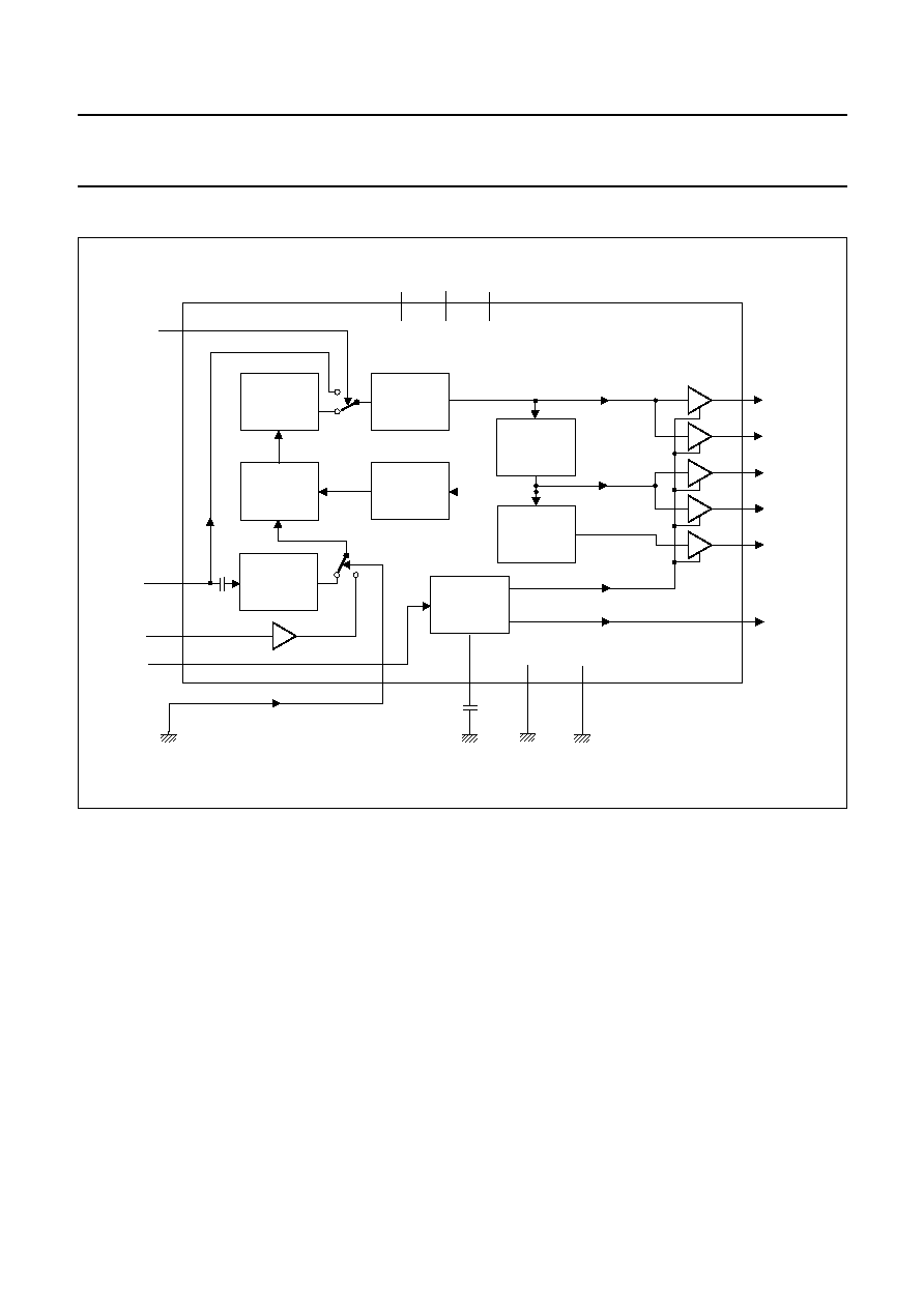
BLOCK DIAGRAM
Fig.1 Block diagram.
handbook, full pagewidth
11
SAA7197
VCO
FREQUENCY
DIVIDER
1 : 2
FREQUENCY
DIVIDER
1 : 2
DELAY
LOOP
FILTER
PHASE
DETECTOR
PRE-FILTER
AND
PULSE
SHAPER
POWER-ON
RESET
LFCO
CE
MS
1
V
DDD1
V
DDD2
V
DDA
5
17
8
7
10
20
15
14
LLCA
LLCB
LLC2A
LLC2B
CREF
RESN
12
4
V
SSA
V
SSD
6, 9, 13, 18
3
PORD
MEH461
2
19
LFCO2
LFCOSEL
16
MS = LOW
FUNCTION DESCRIPTION
The SAA7197 generates all clock signals required for a
digital TV system suitable for the SAA719x family
consisting of an 8-bit analog-to-digital converter (ADC8),
digital video multistandard decoder, square pixel
(DMSD-SQP), digital video colour space converter
(DCSC) and optional extensions. The SAA7197 completes
a system for Desktop Video applications in conjunction
with memory controllers.
The input signal LFCO is a digital-to-analog converted
signal provided by the DMDS-SQPs horizontal PLL. It is
the multiple of the line frequency:
7.38 MHz = 472
◊
f
H
in 50 Hz systems
6.14 MHz = 360
◊
f
H
in 60 Hz systems
LFCO2 (TTL-compatible signal from an external reference
source) can be applied to pin 19 (LFCOSEL = HIGH).
The input signal LFCO or LFCO2 is multiplied by factors 2
or 4 in the PLL (including phase detector, loop filter, VCO
and frequency divider) and output on LLCA (pin7), LLCB
(pin 10), LLC2A (pin 14) and LLC2B (pin 20). The
rectangular output signals have 50% duty factor. Outputs
with equal frequency may be connected together
externally. The clock outputs go HIGH during power-on
reset (and chip enable) to ensure that no output clock
signals are available the PLL has locked-on.
Mode select MS
The LFCO input signal is directly connected to the VCO at
MS = HIGH. The circuit operates as an oscillator and
frequency divider. This function is not tested.
August 1996
4
Philips Semiconductors
Product specification
Clock Generator Circuit for desktop video systems (CGC)
SAA7197
Source select LFCOSEL
Line frequency control signal LFCO (pin 11) is selected by
LFCOSEL = LOW. LFCOSEL = HIGH selects LFCO2
input signal (pin 19). This function is not tested.
Chip enable CE
The buffer outputs are enabled and RESN set HIGH by
CE = HIGH (Fig.4). CE = LOW sets the clock outputs
HIGH and RESN output LOW.
CREF output
2 f
LFCO
output to control the clock dividers of the
DMSD-SQP chip family.
Power-on reset
Power-on reset is activated at power-on, when the supply
voltage decreases below 3.5 V (Fig.4) or when chip enable
is done. The indicator output RESN is LOW for a time
determined by capacitor on pin 3. The RESN signal can be
applied to reset other circuits of this digital TV system.
The LFCO or LFCO2 input signals have to be applied
before RESN becomes HIGH.
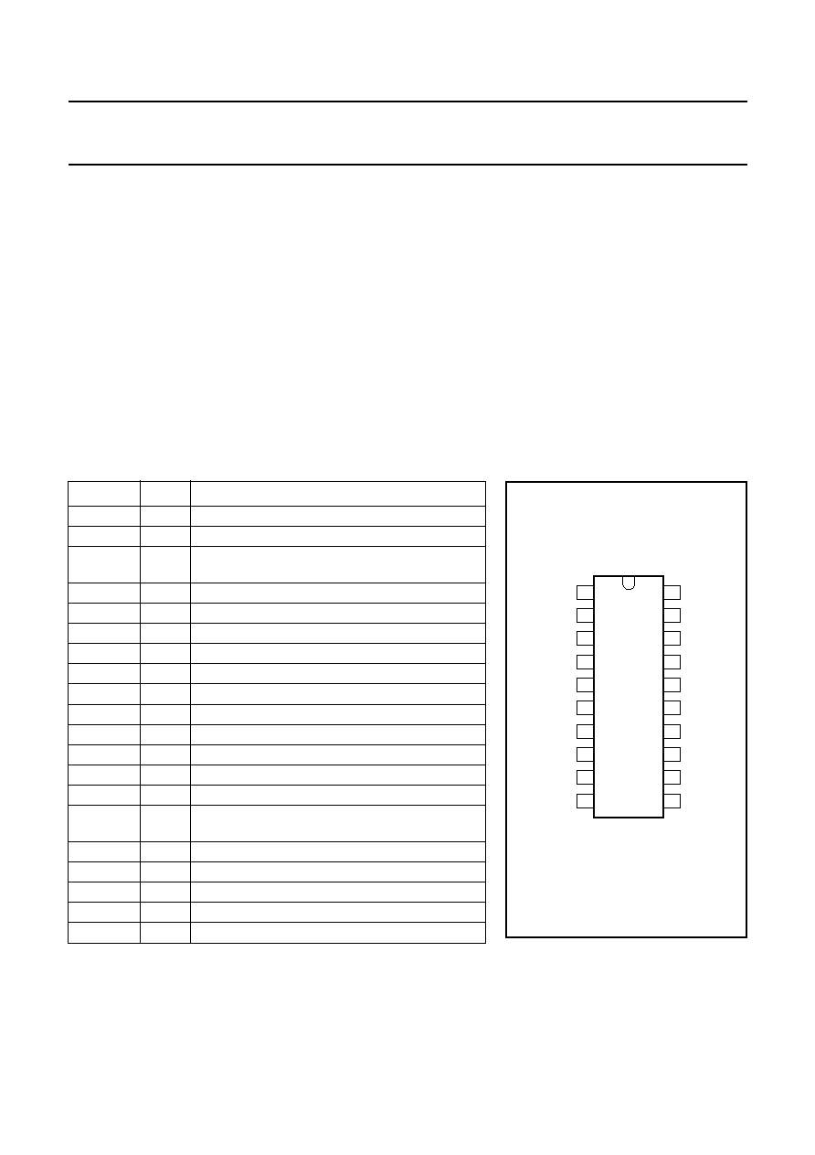
PINNING
Note
1. MS and LFCO2 functions are not tested. LFCO2 is a multiple of
horizontal frequency.
SYMBOL
PIN
DESCRIPTION
MS
1
mode select input (LOW = PLL mode)
(1)
CE
2
chip enable /reset (HIGH = outputs enabled)
PORD
3
power-on reset delay, dependent on external
capacitor
V
SSA
4
analog ground (0 V)
V
DDA
5
analog supply voltage (+5 V)
V
SSD1
6
digital ground 1 (0 V)
LLCA
7
line-locked clock output signal (4 times f
LFCO
)
V
DDD1
8
digital supply voltage 1 (+5 V)
V
SSD2
9
digital ground 2 (0 V)
LLCB
10
line-locked clock output signal (4 times f
LFCO
)
LFCO
11
line-locked frequency control input signal 1
RESN
12
reset output (active-LOW, Fig.4)
V
SSD3
13
digital ground 3 (0 V)
LLC2A
14
line-locked clock output signal 2A (2 times f
LFCO
)
CREF
15
clock reference output, qualifier signal
(2 times f
LFCO
)
LFCOSEL
16
LFCO source select (LOW = LFCO selected)
(1)
V
DDD2
17
digital supply voltage 2 (+5 V)
V
SSD4
18
digital ground 4 (0 V)
LFCO2
19
line-locked frequency control input signal 2
(1)
LLC2B
20
line-locked clock output signal 2B (2 times f
LFCO
)
PIN CONFIGURATION
Fig.2 Pin configuration.
halfpage
SAA7197
MGL505
1
2
3
4
5
6
7
8
9
10
20
19
18
17
16
15
14
13
12
11
MS
CE
PORD
VSSA
VDDA
VSSD1
LLCA
VDDD1
VSSD2
LLCB
LFCO2
VSSD4
VDDD2
LFCOSEL
CREF
LLC2A
VSSD3
RESIN
LFCO
LLC2B
August 1996
5
Philips Semiconductors
Product specification
Clock Generator Circuit for desktop video systems (CGC)
SAA7197
LIMITING VALUES
In accordance with the Absolute Maximum Rating System (IEC 134);
ground pins as well as supply pins together connected.
Note
1. Inputs and outputs are protected against electrostatic discharge in normal handling. However, to be totally safe, it is
recommended to take normal handling precautions appropriate to
"Handling MOS devices".
CHARACTERISTICS
V
DDA
= V
DDD
= 4.5 to 5.5 V; f
LFCO
= 5.5 to 8.0 MHz and T
amb
= 0 to 70
∞
C unless otherwise specified.
SYMBOL
PARAMETER
MIN.
MAX.
UNIT
V
DDA
analog supply voltage (pin 5)
-
0.5
7.0
V
V
DDD
digital supply voltage (pins 8 and 17)
-
0.5
7.0
V
V
diff GND
difference voltage V
DDA
-
V
DDD
-
±
100
mV
V
O
output voltage (I
OM
= 20 mA)
-
0.5
V
DDD
V
P
tot
total power dissipation (DIL20)
0
1.1
W
T
stg
storage temperature range
-
65
150
∞
C
T
amb
operating ambient temperature range
0
70
∞
C
V
ESD
electrostatic handling
(1)
for all pins
-
tbf
V
SYMBOL
PARAMETER
CONDITIONS
MIN.
TYP.
MAX.
UNIT
V
DDA
analog supply voltage (pin 5)
4.5
5.0
5.5
V
V
DDD
digital supply voltage (pins 8 and 17)
4.5
5.0
5.5
V
I
DDA
analog supply current (pin 5)
3
-
9
mA
I
DDD
digital supply current (I
8
+ I
17
)
note 1
10
-
60
mA
V
reset
power-on reset threshold voltage
Fig.4
-
3.5
-
V
Input LFCO (pin 11)
V
11
DC input voltage
0
-
V
DDA
V
V
i
input signal (peak-to-peak value)
1
-
V
DDA
V
f
LFCO
input frequency range
5.5
-
8.0
MHz
C
11
input capacitance
-
-
10
pF
Inputs MS, CE, LFCOSEL and LFCO2 (pins 1, 2, 16 and 19); note 3
V
IL
input voltage LOW
0
-
0.8
V
V
IH
input voltage HIGH
2.0
-
V
DDD
V
f
LFCO2
input frequency range for LFCO2
5.5
-
8.0
MHz
I
LI
input leakage current
LFCOSEL
50
-
150
µ
A
others
-
-
10
µ
A
C
I
input capacitance
-
-
5
pF
Output RESN (pin 12)
V
OL
output voltage LOW
I
OL
= 2 mA
0
-
0.4
V
V
OH
output voltage HIGH
I
OH
=
-
0.5 mA
2.4
-
V
DDD
V
t
d
RESN delay time
C
3
= 0.1
µ
F; Fig.4
20
-
200
ms