 | –≠–ª–µ–∫—Ç—Ä–æ–Ω–Ω—ã–π –∫–æ–º–ø–æ–Ω–µ–Ω—Ç: SAA7199 | –°–∫–∞—á–∞—Ç—å:  PDF PDF  ZIP ZIP |
Document Outline
- FEATURES
- GENERAL DESCRIPTION
- QUICK REFERENCE DATA
- ORDERING INFORMATION
- BLOCK DIAGRAM
- PINNING
- FUNCTIONAL DESCRIPTION
- Colour look-up tables (CLUTs)
- I 2 C-bus format
- Modes of the SAA7199B
- Data input formats
- Accuracy of matrix
- Estimation of noise by quantization
- Normalizing amplifiers in the luminance channel
- Normalizing amplifiers in the chrominance channel
- Modulator
- Functional timing
- Reset
- Disable chip
- LIMITING VALUES
- CHARACTERISTICS
- PACKAGE OUTLINE
- SOLDERING
- DEFINITIONS
- LIFE SUPPORT APPLICATIONS
- PURCHASE OF PHILIPS I 2 C COMPONENTS

DATA SHEET
Product specification
Supersedes data of April 1993
File under Integrated Circuits, IC22
1996 Sep 27
INTEGRATED CIRCUITS
SAA7199B
Digital Video Encoder (DENC)
GENLOCK-capable

1996 Sep 27
2
Philips Semiconductors
Product specification
Digital Video Encoder (DENC)
GENLOCK-capable
SAA7199B
FEATURES
∑
Monolithic integrated CMOS video encoder circuit
∑
Standard MPU (12 lines) and I
2
C-bus interfaces for
controls
∑
Three 8-bit signal inputs PD7 to PD0 for RGB
respectively YUV or indexed colour signals
(Tables 19 to 26)
∑
Square pixel and CCIR input data rates
∑
Band limited composite sync pulses
∑
Three 256
◊
8 colour look-up tables (CLUTs)
for example for gamma correction
∑
External subcarrier from a digital decoder (SAA7151B or
SAA7191B)
∑
Multi-purpose key for real time format switching
∑
Autonomous internal blanking
∑
Optional GENLOCK operation with adjustable horizontal
sync timing and adjustable subcarrier phase
∑
Stable GENLOCK operation in VCR standard playback
mode
∑
Optional still video capture extension
∑
Three suitable video 9-bit digital-to-analog converters
∑
Composite analog output signals CVBS, Y and C for
PAL/NTSC
∑
Line 21 data insertion possible.
GENERAL DESCRIPTION
The SAA7199B encodes digital baseband colour/video
data into analog Y, C and CVBS signals (S-video
included). Pixel clock and data are line-locked to the
horizontal scanning frequency of the video signal.
The circuit can be used in a square pixel or in a consumer
TV application. Flexibility is provided by programming
facilities via MPU-bus (parallel) or I
2
C-bus (serial).
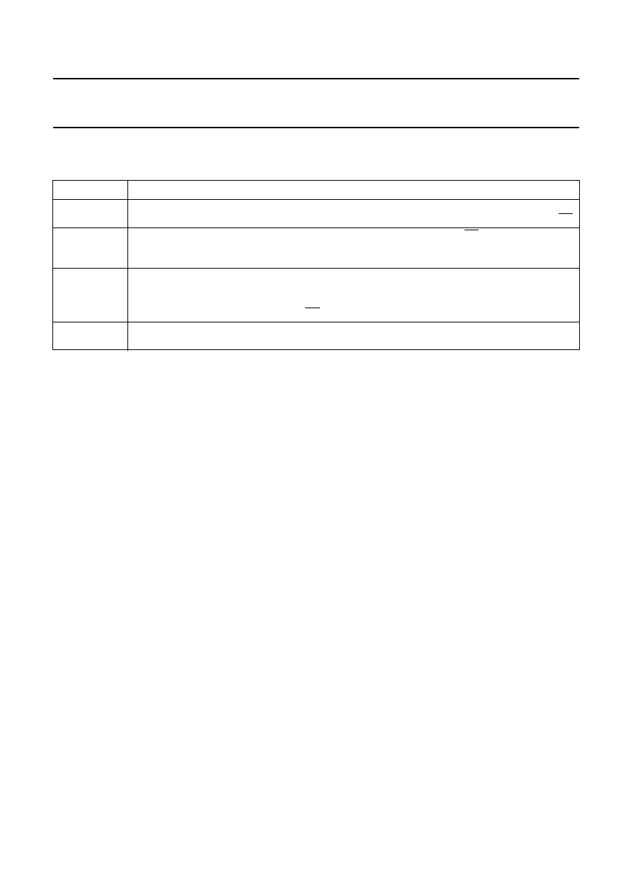
QUICK REFERENCE DATA
ORDERING INFORMATION
SYMBOL
PARAMETER
MIN.
TYP.
MAX.
UNIT
V
DDD
digital supply voltage (pins 2, 21 and 41)
4.5
5.0
5.5
V
V
DDA
analog supply voltage (pins 64, 66, 70 and 72)
4.75
5.0
5.25
V
I
P(tot)
total supply current
-
-
200
mA
V
I
input signal levels
TTL-compatible
V
o
analog output voltage Y, C and CVBS without load (peak-to-peak value)
-
2
-
V
R
L
output load resistance
90
-
-
ILE
LF integral linearity error in output signal (9-bit DAC)
-
-
±
1
LSB
DLE
LF differential linearity error in output signal (9-bit DAC)
-
-
±
0.5
LSB
T
amb
operating ambient temperature
0
-
70
∞
C
TYPE
NUMBER
PACKAGE
NAME
DESCRIPTION
VERSION
SAA7199BWP
PLCC84
plastic leaded chip carrier; 84 leads
SOT189-2
1996 Sep 27
3
Philips Semiconductors
Product specification
Digital Video Encoder (DENC)
GENLOCK-capable
SAA7199B
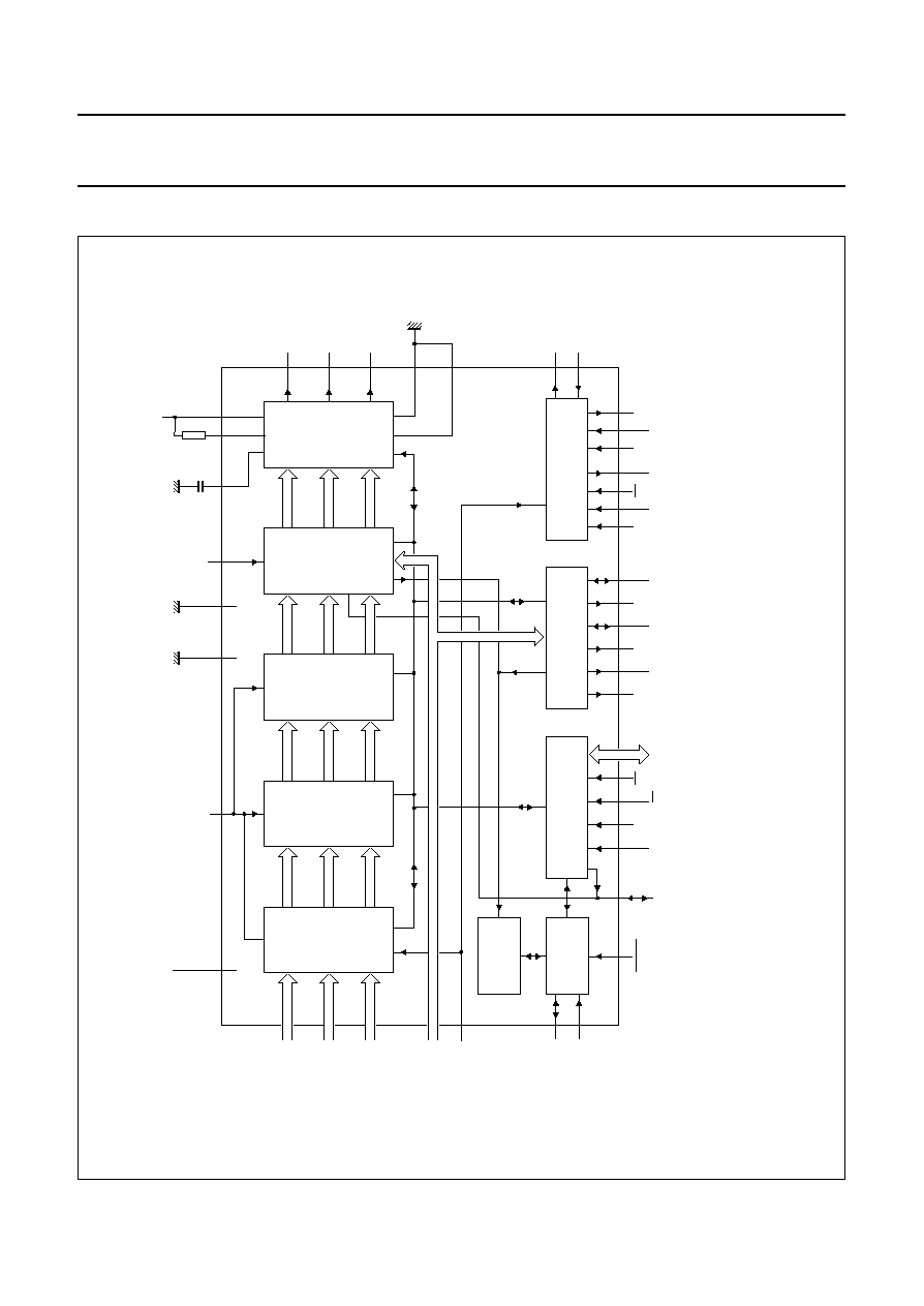
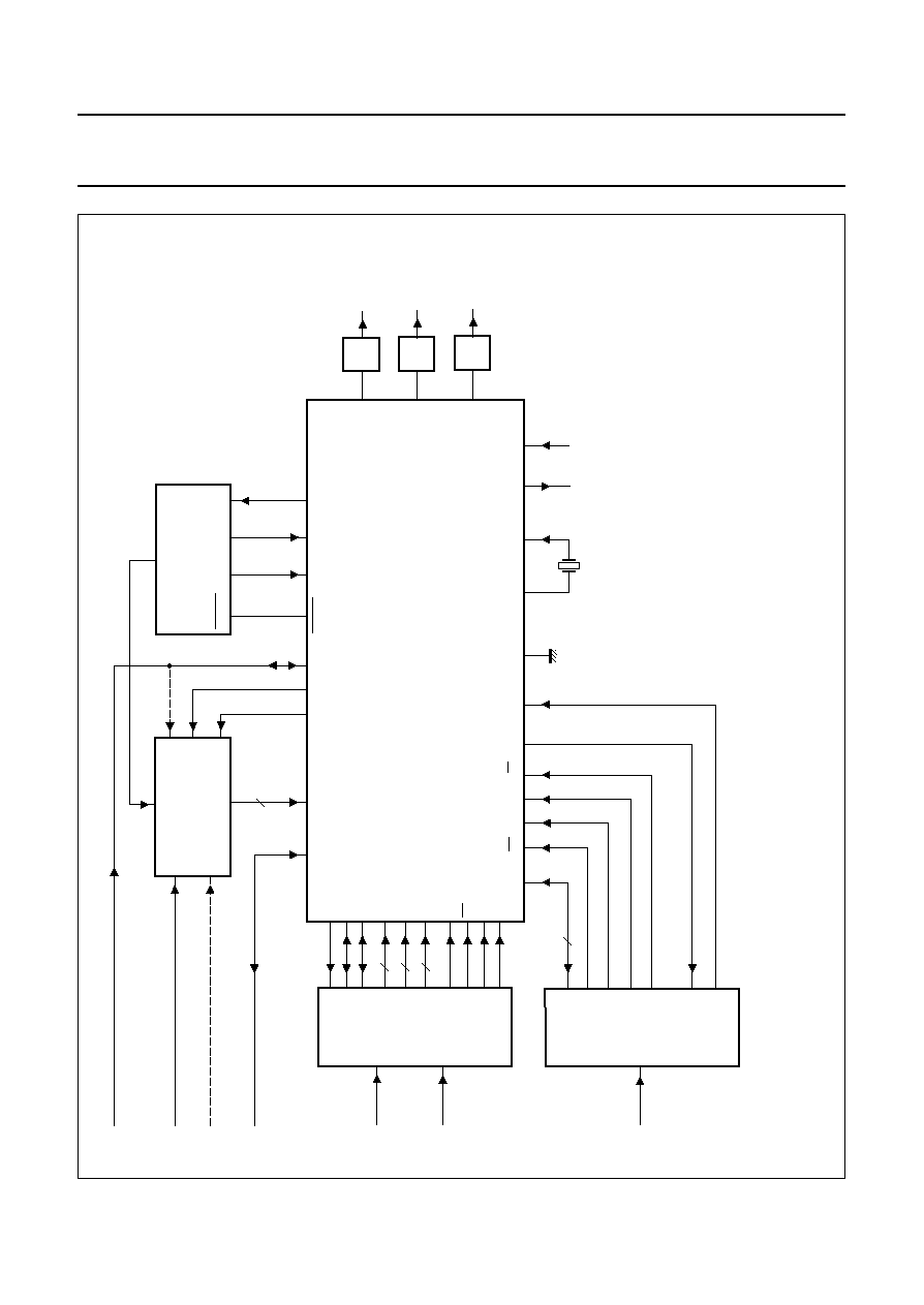
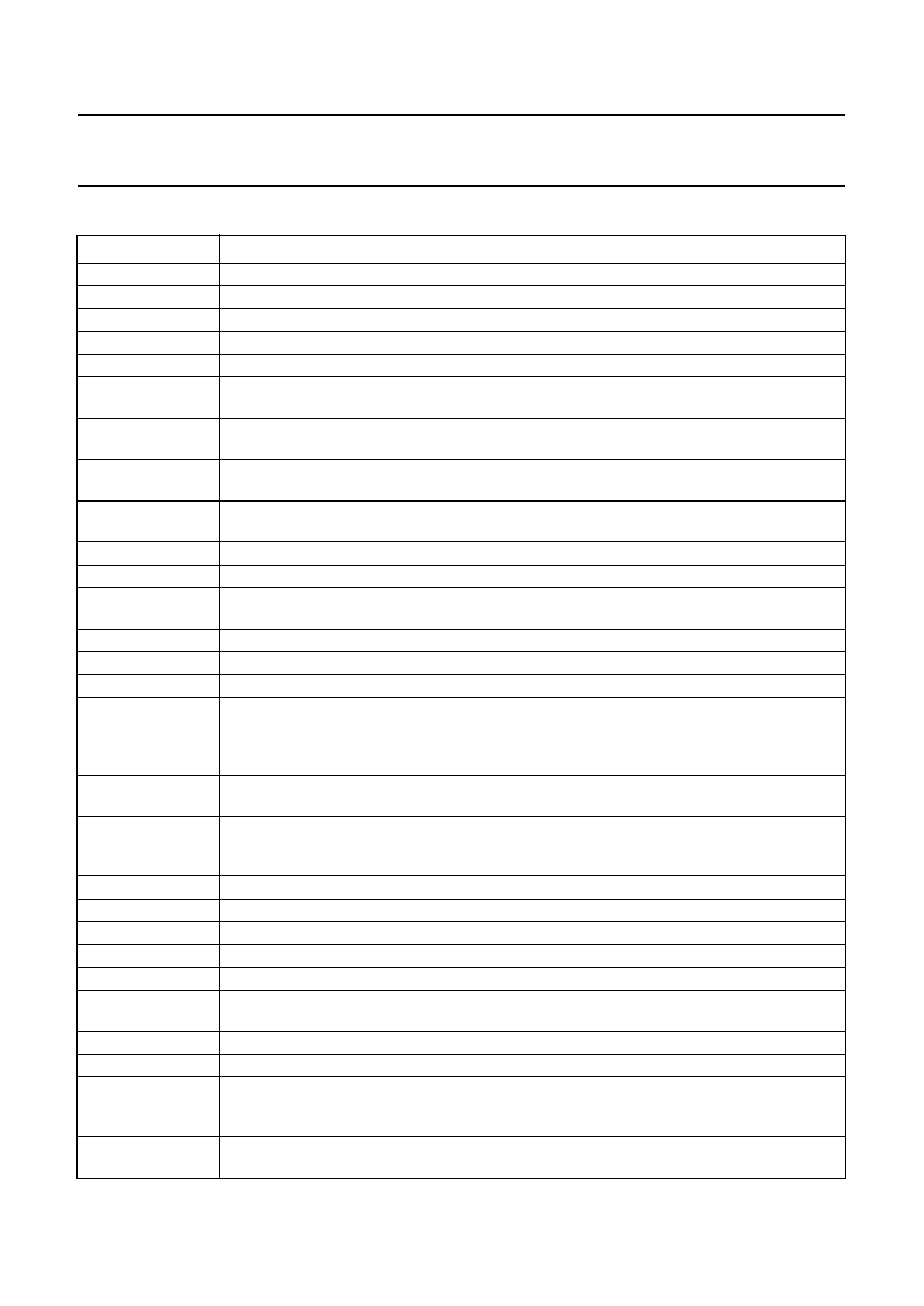
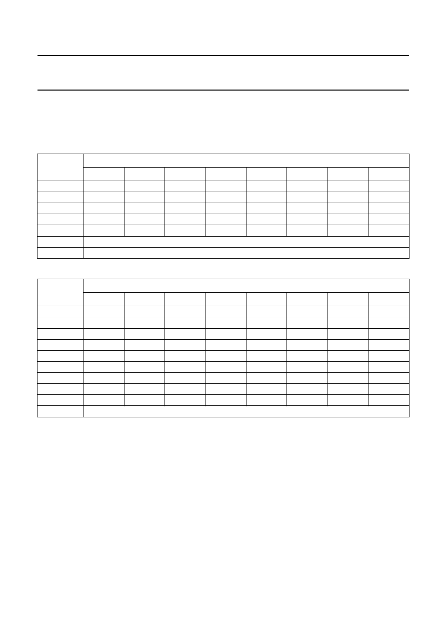
BLOCK DIAGRAM
book, full pagewidth
SDA
SCL
SAA7199B
48
47
STATUS
REGISTER
TRIPLE
DACs
OUTPUT
BUFFERS
CREF
LLC
XTALI
XTALO
MEH416
V
SSA
68
69
Y
C
2, 21, 41
V
SSD1
to V
SSD3
83 to 76
CVBS(7 to 0)
HCL
HSY
HSN
LFCO
+5 V
63
I
2
C-BUS
CONTROL
CONTROL INTERFACE
SYNC PROCESSING
CLOCK INTERFACE
SLT
VSN/CSYN
PIXCLK
CLKIN
CLKO
CLKSEL
60
59
52
49
50
51
23
55
56
3
58
84
61
74
75
36
35
57
54
A0
A1
CLUTS
3 •
256 • 8
INPUT
INTERFACE
ENCODER
MATRIX
D(7 to 0)
20
internal control bus
46 to 43,
40 to 37
CVBS
outputs to
monitor/TV
67
65
66, 70,
72, 64
71
CUR
+5 V
V
DDD1
to V
DDD3
1, 22, 42
KEY
32
11 to 4
19 to 12
31 to 24
PD2(7 to 0)
(1)
(digital green)
PD1(7 to 0)
(1)
(digital red)
PD3(7 to 0)
(1)
(digital blue)
LDV
73
53
V
refL
V
refH
62
3
◊
8-bit input data
I
2
C-bus
MPK
TP
33
34
to/from microcontroller
RTCI
RTCI/
GPSW
RESET
CS
CB
R/W
V
DDA1
to
V
DDA4
Fig.1 Block diagram.
(1)
RGB respectively input formats YUV and indexed colour (Tables
19
to
26).
1996 Sep 27
4
Philips Semiconductors
Product specification
Digital Video Encoder (DENC)
GENLOCK-capable
SAA7199B
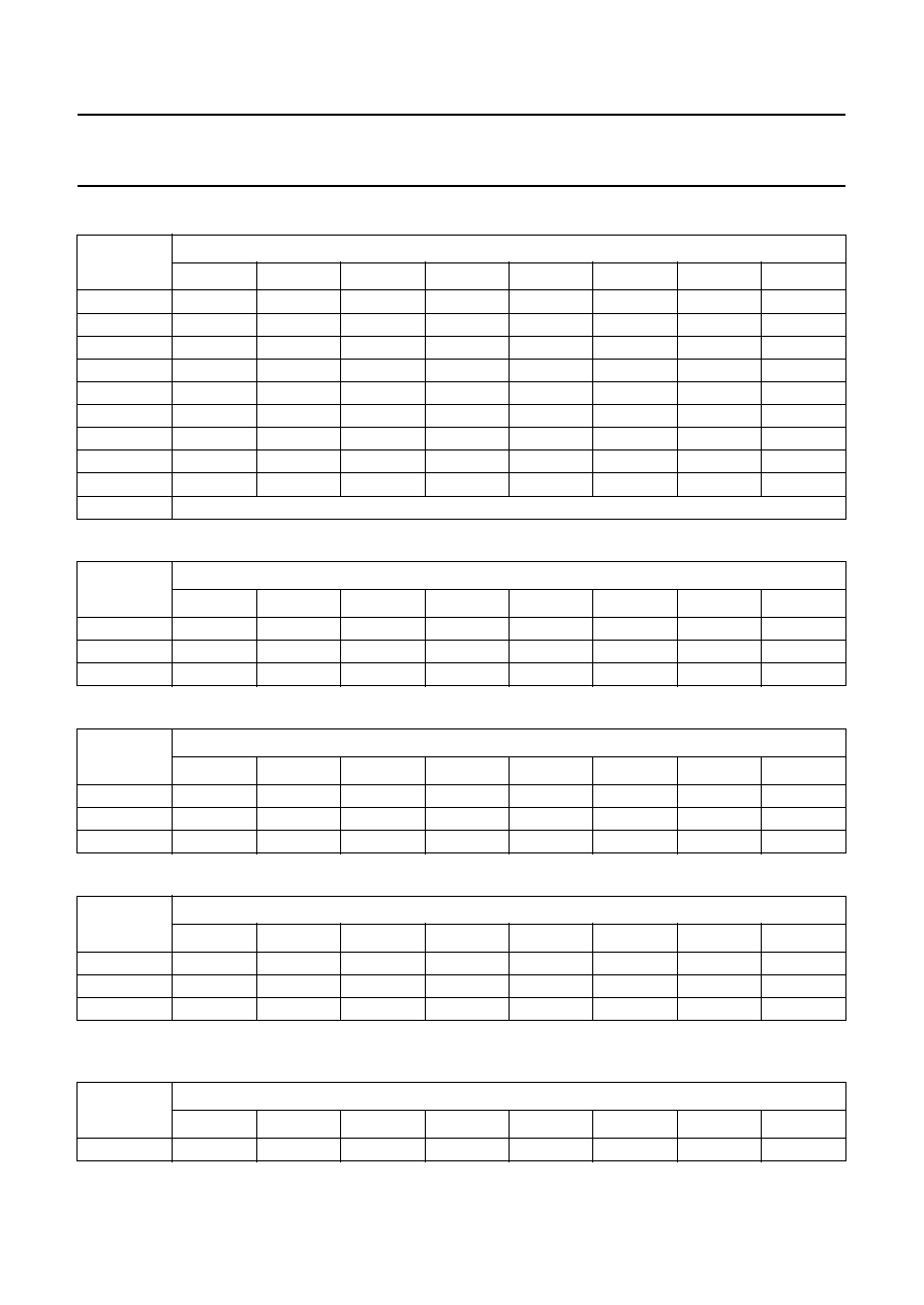
PINNING
SYMBOL
PIN
DESCRIPTION
V
SSD1
1
digital ground 1 (0 V)
V
DDD1
2
digital supply 1 (5 V)
VSN/CSYN
3
vertical sync output (3-state), conditionally composite sync output; active LOW or active HIGH
PD1(0)
4
data 1 input: digital signal R (red) respectively V signal; bit 0 (formats in Tables 19 to 25)
PD1(1)
5
data 1 input: digital signal R (red) respectively V signal; bit 1 (formats in Tables 19 to 25)
PD1(2)
6
data 1 input: digital signal R (red) respectively V signal; bit 2 (formats in Tables 19 to 25)
PD1(3)
7
data 1 input: digital signal R (red) respectively V signal; bit 3 (formats in Tables 19 to 25)
PD1(4)
8
data 1 input: digital signal R (red) respectively V signal; bit 4 (formats in Tables 19 to 25)
PD1(5)
9
data 1 input: digital signal R (red) respectively V signal; bit 5 (formats in Tables 19 to 25)
PD1(6)
10
data 1 input: digital signal R (red) respectively V signal; bit 6 (formats in Tables 19 to 25)
PD1(7)
11
data 1 input: digital signal R (red) respectively V signal; bit 7 (formats in Tables 19 to 25)
PD2(0)
12
data 2 input: digital signal G (green) respectively Y signal or indexed colour data; bit 0
(formats in Tables 19 to 25)
PD2(1)
13
data 2 input: digital signal G (green) respectively Y signal or indexed colour data; bit 1
(formats in Tables 19 to 25)
PD2(2)
14
data 2 input: digital signal G (green) respectively Y signal or indexed colour data; bit 2
(formats in Tables 19 to 25)
PD2(3)
15
data 2 input: digital signal G (green) respectively Y signal or indexed colour data; bit 3
(formats in Tables 19 to 25)
PD2(4)
16
data 2 input: digital signal G (green) respectively Y signal or indexed colour data; bit 4
(formats in Tables 19 to 25)
PD2(5)
17
data 2 input: digital signal G (green) respectively Y signal or indexed colour data; bit 5
(formats in Tables 19 to 25)
PD2(6)
18
data 2 input: digital signal G (green) respectively Y signal or indexed colour data; bit 6
(formats in Tables 19 to 25)
PD2(7)
19
data 2 input: digital signal G (green) respectively Y signal or indexed colour data; bit 7
(formats in Tables 19 to 25)
LDV
20
load data clock input signal to input interface (samples PDn(7 to 0), CB, MPK, KEY and RTCI)
V
DDD2
21
digital supply 2 (5 V)
V
SSD2
22
digital ground 2 (0 V)
CB
23
composite blanking input; active LOW
PD3(0)
24
data 3 input: digital signal B (blue) respectively U signal; bit 0 (formats in Tables 19 to 25)
PD3(1)
25
data 3 input: digital signal B (blue) respectively U signal; bit 1 (formats in Tables 19 to 25)
PD3(2)
26
data 3 input: digital signal B (blue) respectively U signal; bit 2 (formats in Tables 19 to 25)
PD3(3)
27
data 3 input: digital signal B (blue) respectively U signal; bit 3 (formats in Tables 19 to 25)
PD3(4)
28
data 3 input: digital signal B (blue) respectively U signal; bit 4 (formats in Tables 19 to 25)
PD3(5)
29
data 3 input: digital signal B (blue) respectively U signal; bit 5 (formats in Tables 19 to 25)
PD3(6)
30
data 3 input: digital signal B (blue) respectively U signal; bit 6 (formats in Tables 19 to 25)
PD3(7)
31
data 3 input: digital signal B (blue) respectively U signal; bit 7 (formats in Tables 19 to 25)
MPK
32
multi-purpose key input; active HIGH
A0
33
subaddress bit A0 input for microcontroller access (Table 3)

1996 Sep 27
5
Philips Semiconductors
Product specification
Digital Video Encoder (DENC)
GENLOCK-capable
SAA7199B
A1
34
subaddress bit A1 input for microcontroller access (Table 3)
R/W
35
read/write not input signal from microcontroller
CS
36
chip select input for parallel interface; active LOW
D0
37
bidirectional port from/to microcontroller; bit D0
D1
38
bidirectional port from/to microcontroller; bit D1
D2
39
bidirectional port from/to microcontroller; bit D2
D3
40
bidirectional port from/to microcontroller; bit D3
V
DDD3
41
digital supply 3 (5 V)
V
SSD3
42
digital ground 3
D4
43
bidirectional port from/to microcontroller; bit D4
D5
44
bidirectional port from/to microcontroller; bit D5
D6
45
bidirectional port from/to microcontroller; bit D6
D7
46
bidirectional port from/to microcontroller; bit D7
SDA
47
I
2
C-bus data input/output
SCL
48
I
2
C-bus clock input
CLKIN
49
external clock signal input (maximum frequency 60 MHz)
CLKSEL
50
clock source select input
PIXCLK
51
CLKO/2 or conditionally CLKO output signal
CLKO
52
selected clock output signal (LLC or CLKIN)
TP
53
test pin; connected to ground
RESET
54
reset input; active LOW
LLC
55
line-locked clock input signal from external clock generation circuit (CGC)
CREF
56
clock qualifier input of external CGC
GPSW/RTCI
57
general purpose switch output (set via I
2
C-bus or MPU-bus); real time control input, defined
by I
2
C or MPU programming
SLT
58
GENLOCK output flag (3-state): HIGH = sync lost in GENLOCK mode; LOW = otherwise
XTALI
59
crystal oscillator input (26.8 or 24.576 MHz)
XTALO
60
crystal oscillator output
LFCO
61
line frequency control output signal for external CGC
V
refL
62
reference voltage LOW of DACs (resistor chains)
V
refH
63
reference voltage HIGH of DACs (resistor chains)
V
DDA4
64
analog supply 4 for resistor chains of the DACs (5 V)
C
65
chrominance analog output signal
V
DDA1
66
analog supply 1 for output buffer amplifier of DAC1 (5 V)
Y
67
luminance analog output signal
V
SSA
68
analog ground (0 V)
CVBS
69
CVBS analog output signal
V
DDA2
70
analog supply 2 for output buffer amplifier of DAC2 (5 V)
CUR
71
current input for analog output buffers
V
DDA3
72
analog supply 3 for output buffer amplifier of DAC3 (5 V)
KEY
73
key input signal to insert CVBS input signal into encoded CVBS output signal; active HIGH
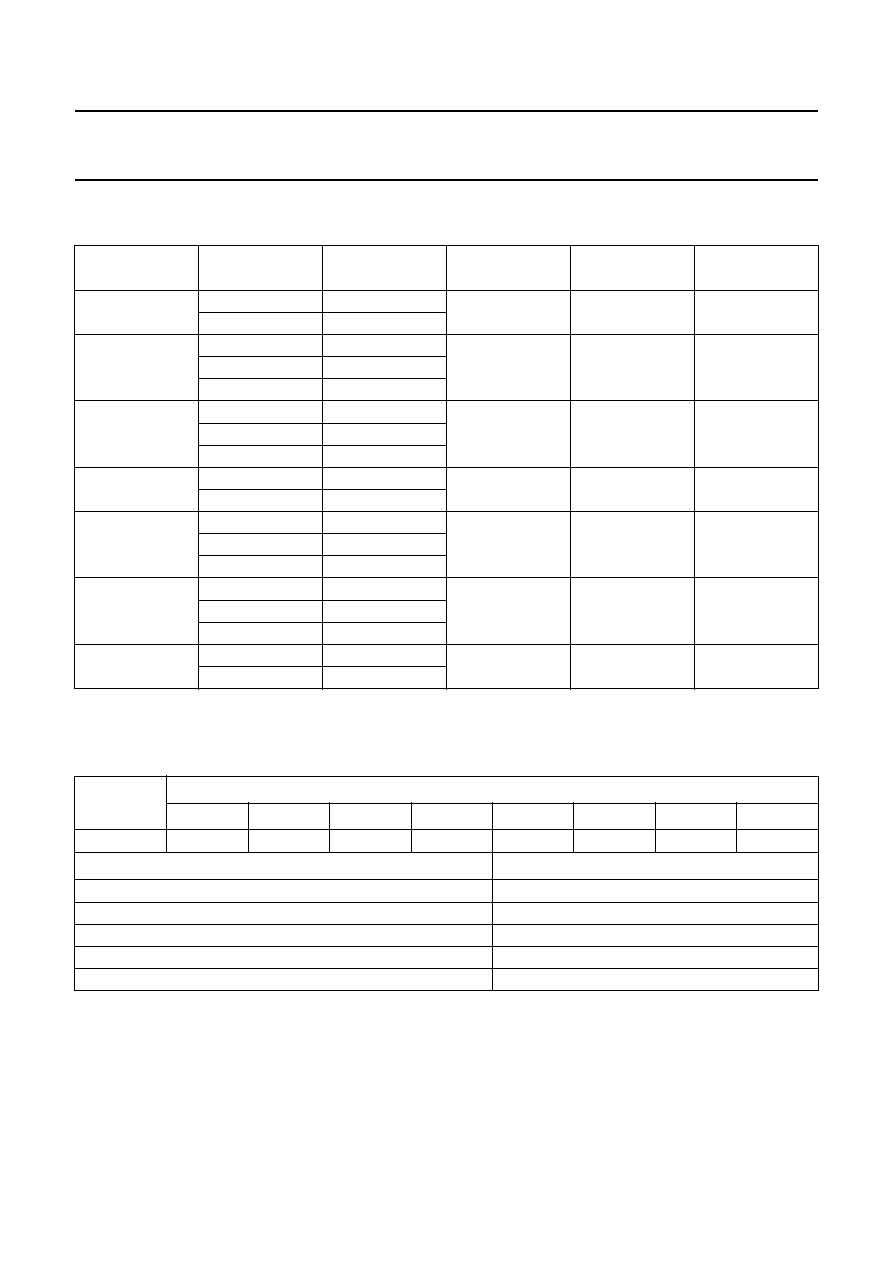
SYMBOL
PIN
DESCRIPTION
1996 Sep 27
6
Philips Semiconductors
Product specification
Digital Video Encoder (DENC)
GENLOCK-capable
SAA7199B
HSY
74
horizontal sync indicator output signal; active HIGH (3-state output to ADC)
HCL
75
horizontal clamping output; active HIGH (3-state output)
CVBS0
76
digital CVBS input signal; bit 0
CVBS1
77
digital CVBS input signal; bit 1
CVBS2
78
digital CVBS input signal; bit 2
CVBS3
79
digital CVBS input signal; bit 3
CVBS4
80
digital CVBS input signal; bit 4
CVBS5
81
digital CVBS input signal; bit 5
CVBS6
82
digital CVBS input signal; bit 6
CVBS7
83
digital CVBS input signal; bit 7
HSN
84
horizontal sync output; active LOW or active HIGH for 60/66/72
◊
PIXCLK at
12.27/13.5/14.75 MHz (3-state output)
SYMBOL
PIN
DESCRIPTION
1996 Sep 27
7
Philips Semiconductors
Product specification
Digital Video Encoder (DENC)
GENLOCK-capable
SAA7199B
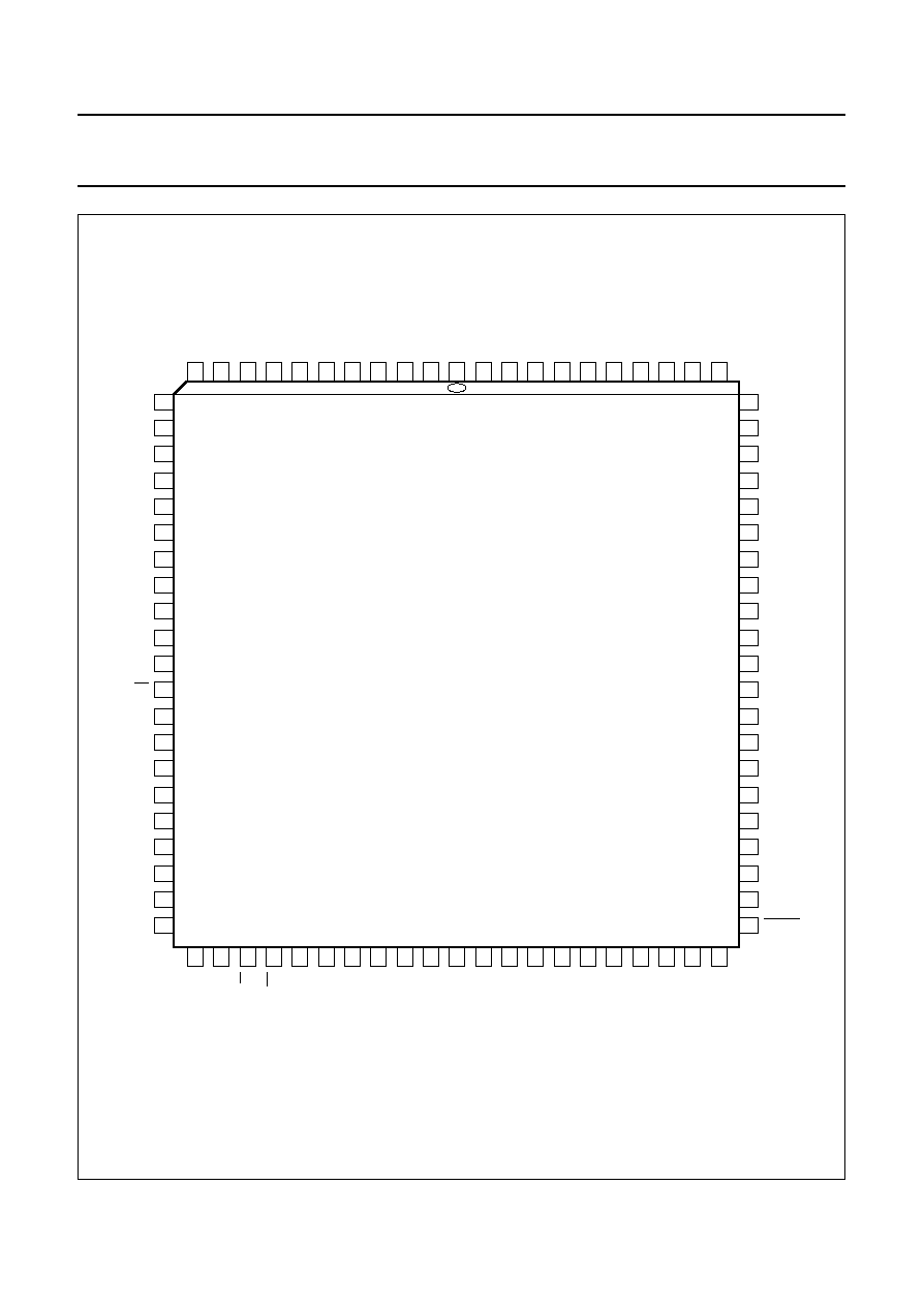
Fig.2 Pin configuration.
handbook, full pagewidth
SAA7199B
MEH417
12
13
14
15
16
17
18
19
20
21
22
23
24
25
26
27
28
29
30
31
32
PD2(0)
PD2(1)
PD2(2)
PD2(3)
PD2(4)
PD2(5)
PD2(6)
PD2(7)
LDV
VDDD2
VSSD2
PD3(0)
PD3(1)
PD3(2)
PD3(3)
PD3(4)
PD3(5)
PD3(6)
PD3(7)
MKP
74
73
72
71
70
69
68
67
66
65
64
63
62
61
60
59
58
57
56
55
54
HSY
KEY
VDDA3
CUR
VDDA2
CVBS
VSSA
Y
VDDA1
C
VDDA4
VrefH
VrefL
LFCO
XTALO
XTALI
SLT
RTCI/
GPSW
CREF
LLC
33
34
35
36
37
38
39
40
41
42
43
44
45
46
47
48
49
50
51
52
53
A0
A1
R/W
CS
D0
D1
D2
D3
V
DDD3
V
SSD3
D4
D5
D6
D7
SDA
SCL
CLKIN
CLKSEL
PIXCLK
CLKO
TP
11
10
9
8
7
6
5
4
3
2
1
84
83
82
81
80
79
78
77
76
75
PD1(7)
PD1(6)
PD1(5)
PD1(4)
PD1(3)
PD1(2)
PD1(1)
PD1(0)
VSN/CSYN
V
DDD1
V
SSD1
HSN
CVBS7
CVBS6
CVBS5
CVBS4
CVBS3
CVBS2
CVBS1
CVBS0
HCL
CB
RESET

1996 Sep 27
8
Philips Semiconductors
Product specification
Digital Video Encoder (DENC)
GENLOCK-capable
SAA7199B
FUNCTIONAL DESCRIPTION
The SAA7199B is a digital video encoder that translates
digital RGB, YUV or 8-bit indexed colour signals into the
analog PAL/NTSC output signals Y (luminance), C
(4.43/3.58 MHz chrominance) and CVBS (composite
signal including sync).
Four different modes are selectable (Table 18):
Stand-alone mode (horizontal and vertical timings are
generated)
Slave mode (stand-alone unit that accepts external
horizontal and vertical timing), and optional real time
information for subcarrier/clock from a digital colour
decoder
GENLOCK mode (GENLOCK capabilities are achieved
in conjunction with determined ICs)
Test mode (only clock signal is required).
The input data rate (pixel sequence) has an integer
relationship to the number of horizontal clock cycles
(Table 1). A sufficient stable external clock signal ensures
correct encoding. The generated clock frequency in the
GENLOCK mode may deviate by
±
7% depending on the
reference signal which is corresponding to its input sync
signal. The clock will be nominal in the GENLOCK mode
when the reference signal is absent (nominal with crystal
oscillator accuracy for TV time constants, and nominal
±
1.4% for VCR time constants).
The on-chip colour conversion matrix provides "
CCIR 601"
code-compatible transcoding of RGB to YUV data.
RGB data out of bounds, with respect to
"CCIR 601"
specification, can be clipped to prevent over-loading of the
colour modulator. RGB data input can be either in linear
colour space or in gamma-corrected colour space.
YUV data must be gamma-corrected in accordance with
"
CCIR 601". This circuit operates primarily in a 24-bit
colour space (3
◊
8-bit) but can also accommodate
different data formats (4 : 1 : 1, 4 : 2 : 2 and 4 : 4 : 4) plus
8-bit indexed pseudo-colour space operations (FMT-bits in
Table 8).
RGB CLUTs on-chip provide gamma-correction and/or
other CLUT functions. They consist of programmable
tables to be loaded independently, and they generate
24-bit gamma-corrected output signals from 24-bit data of
one of the input formats or from 8-bit indexed
pseudo-colour data.
Required modulation is performed. The digital YUV data is
encoded in accordance with standards
"RS-170A"
(composite NTSC) and
"CCIR 624-4" (composite
PAL-B/G). S-video output signal is available (Y/C) also
some sub-standard output signals (STD-bits in Table 12).
A 7.5 IRE set-up level is automatically selected in the
60 Hz mode, but not selected in the 50 Hz mode.
The analog signal outputs can drive directly into
terminated 75
coaxial lines, a passive external filter is
recommended (Figs 3, 13 and 14). Analog post-filtering is
required (LP in Fig.3).
GENLOCK to an external reference signal is achieved by
addition of a video ADC and a clock generator
combination. Thus, the system is enabled to lock on a
stable video source or to a stable VCR source (normal
playback). The SAA7199B, the ADC and the clock
generator combination (Fig.3) form a control loop
achieving a highly stable line-locked clock. The clock has
to be generated by a crystal oscillator without this
availability. The GENLOCK mode is not available in a
single device set-up.
Control interface
The SAA7199B supports a standard parallel MPU
interface and the serial I
2
C-bus interface. The MPU has
direct access to internal control registers and colour
tables. Update is possible at any time, excluding
coincident internal reading and external writing of the
same cell (the current pixel value could be destroyed).
The two interfaces of Table 2 are selected automatically.
However, the I
2
C-bus control is inactive when the MPU
interface is selected by CS = LOW. No simultaneous
access may occur. I
2
C-bus and MPU control complement
each other and have access to common registers
controlled via a common internal bus. The programmer
can use virtually identical programs.
The internal memory space is devided into the look-up
table and the control table, each with its own 8-bit address
register used as a pointer for specific location.
This address register is provided with auto-incrementation
and can be written by only one addressing.
The look-up table contains three banks of 256 bytes.
Therefore, each read or write cycle must access all three
banks in a pre-determined order. The support logic is part
of the control interface.
1996 Sep 27
9
Philips Semiconductors
Product specification
Digital Video Encoder (DENC)
GENLOCK-capable
SAA7199B
Timing (see Fig.3)
The reference to generate internal clocks from LLC in
GENLOCK operation with SAA7197 is CREF
CREF =
.
In this event input CLKSEL is HIGH and the SRC-bit = 1.
In non-GENLOCK operation the signal from CLKIN is used
and LDV is clock reference (input CLKSEL = 0;
SCR-bit = CPR-bit = 0).
Pins LLC and CLKIN are tied together when no switching
between LLC and CLKIN is applied. In Fig.3 it is assumed
that LLC and CLKIN are double the pixel clock frequency
of CREF and LDV respectively.
CREF must be at the same frequency (or constant HIGH
or LOW) when LLC is at pixel clock frequency. CPR-bit = 1
if CLKIN is at pixel clock frequency.
The buffered CLKO signal is always delayed. LLC or
CLKIN signals are in accordance with CLKSEL.
Mapping
The method of mapping external control signals on to the
internal bus is simple. The MPU-bus contains the signals
as shown in Table 4 (names in chip-internal
nomenclature).
LLC
2
-----------
Bit allocation
The Bit Allocation Map (BAM) shows the individual control
signals, used to control the different operational modes of
the circuit. The I
2
C-bus is normally used for control.
The SAA7199B also has an MPU-bus interface for direct
microcontroller connection. The BAM shown in Table 6
resembles the I
2
C-bus type but can be also used for the
parallel bus; the control registers are indexed from
00H to 0FH. Auto-incrementation is applied.
Digital-to-analog converters
The converters use a combination of resistor chains with
low-impedance output buffers. The bottom output voltage
is 200 mV to reduce integral non-linearity errors.
The analog signal, without load on output pin, is between
0.2 and 2.2 V. Figure 16 shows the application for
1.23 V/75
outputs, using the serial 25 + 22
resistors.
Each digital-to-analog converter has its own supply pin for
the purpose of decoupling. V
DDA4
is the supply voltage for
the resistor chains of the three DACs. The accuracy of this
supply voltage directly influences the output amplitudes.
The current CUR into pin 71 is 0.3 mA (V
DDA4
= 5 V;
R
64-71
= 20 k
); a larger current improves the bandwidth
but increases the integral non-linearity.
Table 1
Pixel relationships
Table 2
Access to the control interface
ACTIVE PIXELS
PER LINE
FIELD RATE
(Hz)
MULTIPLES OF LINE
FREQUENCY
PIXCLK OUTPUT SIGNAL
(MHz)
CRYSTAL
(MHz)
640 (square)
60
780
12.27
26.8
720
60
858
13.5
24.576
768
50
944
14.75
26.8
720
50
864
13.5
24.576
SYMBOL
DESCRIPTION
SDA
I
2
C-bus serial data line (bidirectional)
SCL
I
2
C-bus clock line
A1, A0
MPU-bus address inputs
R/W
read/write control input
CS
chip select input; I
2
C-bus disabled when LOW
GPSW
general purpose switch output (bit of control register)
RESET
reset input signal; active-LOW
1996 Sep 27
10
Philips Semiconductors
Product specification
Digital Video Encoder (DENC)
GENLOCK-capable
SAA7199B
Table 3
Address assignment
Table 4
Signals on the internal bus
Table 5
Signals on the internal bus
ADDRESS INPUTS
I
2
C-BUS SUBADDRESS
SELECTION
A1
A0
0
0
00
ADR-CLUT (address register of look-up tables)
0
1
01
DATA-CLUT
1
0
02
ADR-CTRL (index register of control table)
1
1
03
DATA-CTRL
SYMBOL
DESCRIPTION
R/W
select read/write (read = 1; write = 0)
C/T
control table/look-up table (control table = 1; look-up table = 0)
D/A
select data/address (data = 1; address = 0)
DI/DO (0 to 7)
data bus on port inputs/outputs D7 to D0
EN
enable from control interface to synchronize data transfer
INTERNAL PARALLEL BUS PARALLEL INTERFACE
I
2
C-BUS INTERFACE
R/W
R/W (pin 35)
LSB of slave address byte (read = HIGH; write = LOW)
C/T
A1 (pin 34)
X 4 subaddresses after decoding
A/T
A0 (pin 33)
X 4 subaddresses after decoding
DI/DO (0 to 7)
D7 to D0
data bits D7 to D0 for each subaddress
EN
CS and R/W
enable by every 9th clock of sample of SCL
(control of serial-to-parallel conversion)
1996 Sep 27
11
Philips Semiconductors
Product specification
Digital Video Encoder (DENC)
GENLOCK-capable
SAA7199B
book, full pagewidth
D(7 to 0)
SAA7199B
LP
LP
LP
HSN
PIXCLK
VSN
PD1(7 to 0)
PD2(7 to 0)
PD3(7 to 0)
LDV
CB
KEY
MPK
input
data
RAM
INTERFACE
MPU
INTERFACE
data
controls
I
2
C-bus controls
SDA
SCL
A1
SLT
CLKSEL
A0
CVBS1
CVBS2
VIN1
VIN0
D(7 to 0)
CVBS(7 to 0)
TDA8708A (ADC)
HCL
HSY
GPSW
SAA7197 (CGC)
RESET
CREF
LLC
C
LFCO
CREF
LLCA
RESET
CLK
LLC2A
XTALO
XTALI
TP
CLKO
CLKIN
pixel frequency
in non-GENLOCK
mode
(f
pix
or 2f
pix
)
Y
CVBS
Y
CVBS
C
LFCO
analog outputs
(passive filters
optional)
MHA 418
controls
RTCO (from SAA7151B or SAA7191B)
RTCI
(2)
(1)
(1)
GPSW
R/W
CS
8
8
8
8
8
Fig.3 System configuration.
(1)
Not necessary in GENLOCK mode.
(2)
RTCI optional (GPSW not possible).
1996 Sep 27
12
Philips Semiconductors
Product specification
Digital Video Encoder (DENC)
GENLOCK-capable
SAA7199B
Table 6
Bit allocation map (I
2
C-bus access in Table 17)
Notes
1. DF is the default value for a typical programming example: GENLOCK mode for a VCR; non-gamma-corrected RGB
data (real time keying is possible). SLT will be set if there is no horizontal lock.NTSC-M standard with normal colour
bandwidth and 12.2727 MHz pixel rate. CSYN signal will be provided, arriving 8 pixel clocks earlier, to compensate
pipeline delay in the previous RAM interface. The encoded CVBS is 12 clocks earlier than the CVBS reference on
the input of the previous ADC. The CLUTs are bypassed at MPK = HIGH in real time.
2. Read only bits.
3. Reserved.
4. Adjust as required.
INDEX
DATA BYTE
DF
(1)
BINARY
HEX
D7
D6
D5
D4
D3
D2
D1
D0
Input processing
0000 0000
00
VTBY
FMT2
FMT1
FMT0
SCBW
CCIR
MOD1
MOD0
5C
0000 0001
01
TRER7
TRER6
TRER5
TRER4
TRER3
TRER2
TRER1
TRER0
XX
0000 0010
02
TREG7
TREG6
TREG5
TREG4
TREG3
TREG2
TREG1
TREG0
XX
0000 0011
03
TREB7
TREB6
TREB5
TREB4
TREB3
TREB2
TREB1
TREB0
XX
Sync processing
0000 0100
04
SYSEL1 SYSEL0 SCEN
VTRC
NINT
HPLL
HLCK
(2)
OEF
(2)
10
0000 0101
05
0
0
GDC5
GDC4
GDC3
GDC2
GDC1
GDC0
21
0000 0110
06
IDEL7
IDEL6
IDEL5
IDEL4
IDEL3
IDEL2
IDEL1
IDEL0
52
0000 0111
07
0
0
PSO5
PSO4
PSO3
PSO2
PSO1
PSO0
32
Control, clock and output formatter
0000 1000
08
DD
KEYE
SRC
CPR
COKI
IM
GPSW
SRSN
64
0000 1001
09
0
BAME
MPKC1
MPKC0
IEPI
RTSC
RTIN
RTCE
02
0000 1010
(3)
0A
(3)
0
0
0
0
0
0
0
0
00
0000 1011
(3)
0B
(3)
0
0
0
0
0
0
0
0
00
Encoder control
0000 1100
0C
CHPS7
CHPS6
CHPS5
CHPS4
CHPS3
CHPS2
CHPS1
CHPS0
XX
(4)
0000 1101
0D
FSCO7
FSCO6
FSCO5
FSCO4
FSCO3
FSCO2
FSCO1
FSCO0
00
0000 1110
0E
0
0
0
CLCK
(2)
STD3
STD2
STD1
STD0
0C
0000 1111
(3)
0F
(3)
0
0
0
0
0
0
0
0
1996 Sep 27
13
Philips Semiconductors
Product specification
Digital Video Encoder (DENC)
GENLOCK-capable
SAA7199B
Table 7
Function of registers bits of Table 6
BIT
FUNCTION
Index 00 VTBY
video look-up table by-pass: 0 = not bypassed; 1 = bypassed (logically OR-ed with MPK)
FMT2 to FMT0
input formats see Table 8
SCBW
chrominance bandwidth: 0 = enhanced; 1 = standard
CCIR
select level: 0 = DMSD2 levels; 1 = CCIR levels
MOD1 to MOD0
select mode see Table 9
Index 01
TRER7 to TRER0
test register red (read/write via MPU-bus; write only via I
2
C-bus)
Index 02
TREG7 to TREG0
test register green (read/write via MPU-bus; write only via I
2
C-bus)
Index 03
TREB7 to TREB0
test register blue (read/write via MPU-bus; write only via I
2
C-bus)
Index 04
SYSEL1 to SYSEL0
sync select see Table 10
SCEN
sync/clamping (HSY/HCL) enable: 0 = disabled (set to HIGH); 1 = enabled
VTRC
select TV/VTR mode: 0 = TV mode (slow); 1 = VTR mode (fast)
NINT
select interlace of encoded signal: 0 = interlaced (262.5/262.5 or 312.5/312.5);
1 = non-interlaced (262/262 or 312/312 in modes 1 and 3 only)
HPLL
select horizontal lock: 0 = lock enabled; 1 = lock disabled (crystal reference)
OEF
status bit field organization (to be read): 0 = even field; 1 = odd field
HLCK
status bit sync indication (to be read): 0 = locked to external sync; 1 = external sync lost
Index 05
GDC5 to GDC0
GENLOCK delay compensation; note 1: data 00 to 3F equals timing of CVBS output signal
which is (46
-
GDC) pixel clocks = t
ofs
earlier with respect to reference point t
REF1
.
(t
REF1
corresponds to the falling edge of the horizontal sync pulse of CVBS input signal; t
ofs
is
designated for propagation delay of external GENLOCK source, Fig.10).
Index 06
IDEL7 to IDEL0
increment delay: update of line-locked clock frequency (Table 6, data `43' hex recommended)
Index 07
PSO7 to PSO0
Phase sync in output signal, note 1: data 00 to 3F equals to active slope of HSN, VSN/CSYN is
(58
-
PSO) pixel clocks = t
Rint
earlier with respect to reference point t
REF2
(t
REF2
corresponds to
PSO = 58; t
Rint
is designated for pipeline delay of the feeding RAM interface, Fig.10).
Index 08 DD
digital video encoder disable: 0 = enabled; 1 = disabled
KEYE
keying enable: 0 = disabled; 1 = enabled (logically AND-connected with KEY)
SRCC
clock source: 0 = external system clock; 1 = DTV2 system clock
CPR
clock phase reference: 0 = LDV is input (pin 20); 1 = LDV is not
COKI
colour-killer: 0 = colour on; 1 = colour off (subcarrier is switched off)
IM
interrupt mask: 1 = interrupt not masked at sync lost (pin 58) 0 = interrupt masked at sync lost
(pin 58)
GPSW
general purpose switch at bit RTIN = 1: 0 = pin 57 LOW; 1 = pin 57 HIGH
SRSN
software reset: 0 = no reset; 1 = reset (see "Reset" procedure)
Index 09 BAME
Burst amplitude indication: 0 = burst amplitude measurement is overridden; colour lock always
assumed; 1 = burst amplitude is used to control the CLCK status bit, recommended for
reference signal without subcarrier burst (pure black and white) in order to avoid PLL hunting.
MPKC1 to MPKC0
multipurpose key control: with MKP = LOW (pin 32) all functions are as given by software
programming; MKP = HIGH sets in real time with respect to PDn (7 to 0); functions see Table 11
1996 Sep 27
14
Philips Semiconductors
Product specification
Digital Video Encoder (DENC)
GENLOCK-capable
SAA7199B
Note
1. Field blanking (Figs 11 and 12): normally, video to be encoded should not become active after the active edge of
VSN or CSYN before line 22.5 at 50 Hz (line 18 at 60 Hz). Total internal field blanking is 11 lines at 50 Hz (13 lines
at 60 Hz).
Table 8
Input formats
Table 9
Select mode
IEPI
polarity of external PAL-ID signal (H/2 signal) from RTCI input (pin 57): 0 = not inverted;
1 = inverted
RTSC
Real time select control: 0 = real time control HPLL increment is selected, which means,
information concerning actual clock frequency from the digital colour decoder is received
(SAA7151B or SAA7191B); the corresponding subcarrier frequency is calculated; 1 = real time
control FSC increment with PAL-ID is selected, which means, information concerning actual
subcarrier frequency and PAL-ID from the digital colour decoder is received (SAA7151B or
SAA7191B).
RTIN
select real time control input: 0 = pin 57 is input for RTCI signal; 1 = pin 57 is port output GPSW
RTCE
real time control enabled: 0 = disabled; 1 = enabled (RTIN = 0)
Index 0C
CHPS7 to CHPS0
phase adjustment between chrominance output signal and reference: 00 to FF equals
0 to 358.59375 degrees in steps of 1.40625 degrees
Index 0D
FSC7 to FSC0
fine adjustment of subcarrier frequency in non-GENLOCK modes: 00 to 7F increasing and
FF to 80 decreasing equal approximately to 450
◊
10
-6
of the subcarrier frequency in 256 steps
Index 0E CLCK
lock to external chrominance (to be read): 0 = possible; 1 = not possible
STD3 to STD0
colour encoding standards; see Table 12
-
status bits to be read via I
2
C-bus: see Table 15
-
status bits to be read by microcontroller: all registers from 00 up to 0F can be read via
MPU-bus, read only bits are OEF, HCLK (index 04) and CLCK (index 0E)
FMT2
FMT1
FMT0
FORMAT
0
0
0
YUV 4 : 1 : 1 format; DMSD2 compatible
0
0
1
YUV 4 : 1 : 1 format; customized
0
1
0
YUV 4 : 2 : 2 format; DMSD2 compatible
0
1
1
YUV 4 : 2 : 2 format; customized
1
0
0
YUV 4 : 4 : 4 format
1
0
1
RGB 4 : 4 : 4 format
1
1
0
reserved
1
1
1
8-bit indexed colour
MOD1
MOD0
MODE
0
0
GENLOCK mode
0
1
stand alone mode
1
0
slave mode
1
1
test mode
BIT
FUNCTION
1996 Sep 27
15
Philips Semiconductors
Product specification
Digital Video Encoder (DENC)
GENLOCK-capable
SAA7199B
Table 10 Sync select
Table 11 Multi-purpose key control
Table 12 Colour encoding standards
Colour look-up tables (CLUTs)
The CLUTs consist of RAM tables. The RAM tables can be loaded with X = 0 to 255 in accordance with equation 1 for
the signals R, G and B. Gamma-correction (pre-distortion) by the following equation:
Y = NINT (b + a
◊
X1
1/g
); Y(X
16) = 16; Y(X
235) = 235 (equation 1) with g = 2.2:
;
b = 16
-
a
◊
16
-
2.2
The RAM tables are loaded via MPU-bus or via I
2
C-bus (Table 17).
SYSEL1 SYSEL0
SYNCHRONIZED FROM
0
0
CSYN (active LOW; pin 3)
0
1
HSN and VSN (active LOW; pins 84 and 3)
1
0
CSYN (active HIGH; pin 3)
1
1
HSN and VSN (active HIGH; pins 84 and 3)
SET BY BITS
IN FUNCTION BLOCKS INPUT
FORMATTER
CLUTs
MATRIX
LEVEL
MATCHING
MPKC1
MPKC0
0
0
control via CCIR bit and FMT bits bypass
control via FMT bits control via CCIR bit
0
1
format 5 (RGB) CCIR level
active,
no indexed colour
active
CCIR level
1
X
format 7 (indexed colour)
CCIR level
active,
no indexed colour
active
CCIR level
STD3
STD2
STD1
STD0
STANDARD
0
0
0
0
NTSC 4.43; 60 Hz; SQP (12.27 MHz)
0
0
0
1
NTSC 4.43; 50 Hz; SQP (14.75 MHz)
0
0
1
0
PAL-B/G 4.43; 50 Hz; SQP (14.75 MHz)
0
0
1
1
NTSC 4.43; 60 Hz; CCIR (13.5 MHz)
0
1
0
0
NTSC 4.43; 50 Hz; CCIR (13.5 MHz)
0
1
0
1
PAL-B/G 4.43; 50 Hz; CCIR (13.5 MHz)
0
1
1
0
reserved
0
1
1
1
reserved
1
0
0
0
PAL-M; 60 Hz; SQP (12.27 MHz)
1
0
0
1
PAL-M; 60 Hz; CCIR (13.5 MHz)
1
0
1
0
PAL-N; 50 Hz; CCIR (13.5 MHz)
1
0
1
1
PAL-N; 50 Hz; SQP (14.75 MHz)
1
1
0
0
NTSC-M; 60 Hz; SQP (12.27 MHz)
1
1
0
1
NTSC-M; 60 Hz; CCIR (13.5 MHz)
1
1
1
0
reserved
1
1
1
1
reserved
a
219
235
2.2
≠
16
2.2
≠
≠
----------------------------------------
=
1996 Sep 27
16
Philips Semiconductors
Product specification
Digital Video Encoder (DENC)
GENLOCK-capable
SAA7199B
I
2
C-bus format
Table 13 I
2
C-bus address; see Table 14
Table 14 Explanation of Table 13
Notes
1. X is the read/write control bit; X = 0 is order to write (the circuit is slave receiver); X = 1 is order to read (the circuit is
slave transmitter).
2. If more than 1 byte DATA is transmitted, then auto-increment of the subaddress is performed.
Table 15 I
2
C-bus status byte (address byte B1)
Table 16 Function of the bits in Table 15
Table 17 I
2
C-bus write bytes (address byte B0)
S
SLAVE ADDRESS
ACK
SUBADDRESS
ACK
DATA 0
ACK
--------
DATA n
ACK
P
PART
DESCRIPTION
S
START condition
Slave address
1 0 1 1 0 0 0 X (note 1)
ACK
acknowledge, generated by the slave
Subaddress (note 2)
subaddress byte (Table 17)
DATA
data byte (Table 6)
--------
continued data bytes and ACKs
P
STOP condition
FUNCTION
STATUS BYTE
D7
D6
D5
D4
D3
D2
D1
D0
Read status
0
0
0
0
FFOS
OEF
CLCK
HLCK
BIT
FUNCTION
FFOS
first field of sequence: 0 = false; 1 = first of 4 fields for NTSC (first of 8 fields for PAL). FFOS is not
valid for non-interlaced signals.
OEF
field organization: 0 = even field; 1 = odd field
CLCK
lock to external chrominance: 0 = possible; 1 = not possible
HLCK
sync indication: 0 = locked to external sync; 1 = external sync lost
ACCESS
DESCRIPTION OF BYTE
Control registers address byte B0 subaddress byte 02 index byte (00 to 0F); Table 6
data bytes
(auto-increment)
CLUTs registers
address byte B0 subaddress byte 00 CLUT address bytes
(00 to FF)
3 data bytes for one RGB
sequence (auto-increment)
1996 Sep 27
17
Philips Semiconductors
Product specification
Digital Video Encoder (DENC)
GENLOCK-capable
SAA7199B
Modes of the SAA7199B
Table 18 The four different modes of the SAA7199B
R
ELATIONSHIP BETWEEN HORIZONTAL FREQUENCY AND COLOUR SUBCARRIER FREQUENCY IN NON
-GENLOCK
MODE
1. Internal subcarrier frequency with n = integer
PAL: f
SC
= f
H
(n/4 + 1/625) respectively f
H
(n/4 + 1/525)
NTSC: f
SC
= f
H
(n/2)
Necessary conditions: non-GENLOCK mode; RTCE = 0, FSCO = 00H; phase coupling of the two frequencies is
given by a definite phase reset every 8th field at PAL (4th field at NTSC).
FSCO
00H adjusts the subcarrier frequency, phase reset is disabled and phase between f
SC
and f
H
is not constant.
2. External subcarrier frequency
f
SC
is given by RTCI real time input from a digital colour decoder
Necessary conditions: Slave mode; RTCE = 1, RTSC = 1. The 8th respectively 4th field reset is enabled at
FSCO = 00H (disabled at FSCO
00H). The subcarrier frequency is not influenced by FSCO bits, but is given by
real time increment.
3. External HPLL increment
f
SC
is calculated by RTCI real time input signal from a digital colour decoder. The frequency of f
SC
depends on the
absolute crystal frequency value used by the digital colour decoder.
Necessary conditions: Slave mode; RTCE = 1, RTSC = 0. The 8th respectively 4th field reset is enabled at
FSCO = 00H (disabled at FSCO
00H). The subcarrier frequency is influenced by FSCO bits.
The absolute phase relationship between sync and subcarrier (colour burst output) can be influenced in all three events
by CHPS7 to CHPS0 register byte (index 0C).
MODE
DESCRIPTION
Stand alone
The SAA7199B receives a line-locked clock CLKIN and generates CSYN or HSN/VSN output
signals, which trigger the RGB or the YUV source signal to provide data and composite blanking CB.
Slave
The SAA7199B receives the line-locked clock CLKIN, CSYN or HSN/VSN, CB and data from an
RGB or YUV source. The sync inputs are edge-sensitive; their minimum active length is 1 PIXCLK.
A real time control signal RTCI is received from a digital colour decoder as an option.
GENLOCK
Horizontal and vertical sync plus colour are locked on a received CVBS reference signal. The CVBS
reference signal also generates a line-locked clock by the SAA7197 clock generator. Auxiliary
signals HCL and HSY plus CSYN or HSN/VSN are generated to trigger the RGB or the YUV source
providing data and composite blanking CB.
Test
Similar to stand alone mode, but the contents of the test registers TRER, TREG and TREB consists
of data to be encoded. VSN/CSYN and HSN outputs are in 3-state condition.
1996 Sep 27
18
Philips Semiconductors
Product specification
Digital Video Encoder (DENC)
GENLOCK-capable
SAA7199B
Data input formats
One clock cycle equals 12.27 MHz, 13.5 MHz or 14.75 MHz; Cb = (B
-
Y) equals U; Cr = (R
-
Y) equals V; (n) = number
of pixels.
Table 19 Format 0; DMSD2 compatible YUV 4 : 1 : 1 format (FMT-bits in index 00 = 000)
Table 20 Format 1; customized YUV 4 : 1 : 1 format (FMT-bits in index 00 = 001)
INPUT
SIGNAL
CLOCK CYCLE (PIXEL SEQUENCE)
0
1
2
3
4
5
6
7
PD2(7 to 0)
Y(0)
Y(1)
Y(2)
Y(3)
Y(4)
Y(5)
Y(6)
Y(7)
PD3(7)
Cb7(0)
Cb5(0)
Cb3(0)
Cb1(0)
Cb7(4)
Cb5(4)
Cb3(4)
Cb1(4)
PD3(6)
Cb6(0)
Cb4(0)
Cb2(0)
Cb0(0)
Cb6(4)
Cb4(4)
Cb2(4)
Cb0(4)
PD3(5)
Cr7(0)
Cr5(0)
Cr3(0)
Cr1(0)
Cr7(4)
Cr5(4)
Cr3(4)
Cr1(4)
PD3(4)
Cr6(0)
Cr4(0)
Cr2(0)
Cr0(0)
Cr6(4)
Cr4(4)
Cr2(4)
Cr0(4)
PD3(3 to 0)
not used
PD1(7 to 0)
not used
INPUT
SIGNAL
CLOCK CYCLE (PIXEL SEQUENCE)
0
1
2
3
4
5
6
7
PD2(7 to 0)
Y(0)
Y(1)
Y(2)
Y(3)
Y(4)
Y(5)
Y(6)
Y(7)
PD3(7)
Cb7(0)
-
Cr7(0)
-
Cb7(4)
-
Cr7(4)
-
PD3(6)
Cb6(0)
-
Cr6(0)
-
Cb6(4)
-
Cr6(4)
-
PD3(5)
Cb5(0)
-
Cr5(0)
-
Cb5(4)
-
Cr5(4)
-
PD3(4)
Cb4(0)
-
Cr4(0)
-
Cb4(4)
-
Cr4(4)
-
PD3(3)
Cb3(0)
-
Cr3(0)
-
Cb3(4)
-
Cr3(4)
-
PD3(2)
Cb2(0)
-
Cr2(0)
-
Cb2(4)
-
Cr2(4)
-
PD3(1)
Cb1(0)
-
Cr1(0)
-
Cb1(4)
-
Cr1(4)
-
PD3(0)
Cb0(0)
-
Cr0(0)
-
Cb0(4)
-
Cr0(4)
-
PD1(7 to 0)
not used
1996 Sep 27
19
Philips Semiconductors
Product specification
Digital Video Encoder (DENC)
GENLOCK-capable
SAA7199B
Table 21 Format 2; DMSD2 compatible YUV 4 : 2 : 2 format (FMT-bits in index 00 = 010)
Table 22 Format 3; customized YUV 4 : 2 : 2 format (FMT-bits in index 00 = 011)
Table 23 Format 4; YUV 4 : 4 : 4 format (FMT-bits in index 00 = 100)
Table 24 Format 5; RGB 4 : 4 : 4 format (FMT-bits in index 00 = 101)
Table 25 Format 7; indexed colour format (FMT-bits in index 00 = 111), input codes 0 to 255 are allowed, output code
of CLUTs should preferably be the same as given in format 5
INPUT
SIGNAL
CLOCK CYCLE (PIXEL SEQUENCE)
0
1
2
3
4
5
6
7
PD2(7 to 0)
Y(0)
Y(1)
Y(2)
Y(3)
Y(4)
Y(5)
Y(6)
Y(7)
PD3(7)
Cb7(0)
Cr7(0)
Cb7(2)
Cr7(2)
Cb7(4)
Cr7(4)
Cb7(6)
Cr7(6)
PD3(6)
Cb6(0)
Cr6(0)
Cb6(2)
Cr6(2)
Cb6(4)
Cr6(4)
Cb6(6)
Cr6(6)
PD3(5)
Cb5(0)
Cr5(0)
Cb5(2)
Cr5(2)
Cb5(4)
Cr5(4)
Cb5(6)
Cr5(6)
PD3(4)
Cb4(0)
Cr4(0)
Cb4(2)
Cr4(2)
Cb4(4)
Cr4(4)
Cb4(6)
Cr4(6)
PD3(3)
Cb3(0)
Cr3(0)
Cb3(2)
Cr3(2)
Cb3(4)
Cr3(4)
Cb3(6)
Cr3(6)
PD3(2)
Cb2(0)
Cr2(0)
Cb2(2)
Cr2(2)
Cb2(4)
Cr2(4)
Cb2(6)
Cr2(6)
PD3(1)
Cb1(0)
Cr1(0)
Cb1(2)
Cr1(2)
Cb1(4)
Cr1(4)
Cb1(6)
Cr1(6)
PD3(0)
Cb0(0)
Cr0(0)
Cb0(2)
Cr0(2)
Cb0(4)
Cr0(4)
Cb0(6)
Cr0(6)
PD1(7 to 0)
not used
INPUT
SIGNAL
CLOCK CYCLE (PIXEL SEQUENCE)
0
1
2
3
4
5
6
7
PD2(7 to 0)
Y(0)
Y(1)
Y(2)
Y(3)
Y(4)
Y(5)
Y(6)
Y(7)
PD3(7 to 0)
Cb(0)
-
Cb(2)
-
Cb(4)
-
Cb(6)
-
PD1(7 to 0)
Cr(0)
-
Cr(2)
-
Cr(4)
-
Cr(6)
-
INPUT
SIGNAL
CLOCK CYCLE (PIXEL SEQUENCE)
0
1
2
3
4
5
6
7
PD2(7 to 0)
Y(0)
Y(1)
Y(2)
Y(3)
Y(4)
Y(5)
Y(6)
Y(7)
PD3(7 to 0)
Cb(0)
Cb(1)
Cb(2)
Cb(3)
Cb(4)
Cb(5)
Cb(6)
Cb(7)
PD1(7 to 0)
Cr(0)
Cr(1)
Cr(2)
Cr(3)
Cr(4)
Cr(5)
Cr(6)
Cr(7)
INPUT
SIGNAL
CLOCK CYCLE (PIXEL SEQUENCE)
0
1
2
3
4
5
6
7
PD2(7 to 0)
R(0)
R(1)
R(2)
R(3)
R(4)
R(5)
R(6)
R(7)
PD3(7 to 0)
G(0)
G(1)
G(2)
G(3)
G(4)
G(5)
G(6)
G(7)
PD1(7 to 0)
B(0)
B(1)
B(2)
B(3)
B(4)
B(5)
B(6)
B(7)
INPUT
SIGNAL
CLOCK CYCLE (PIXEL SEQUENCE)
0
1
2
3
4
5
6
7
PD2(7 to 0)
INC(0)
INC(1)
INC(2)
INC(3)
INC(4)
INC(5)
INC(6)
INC(7)
1996 Sep 27
20
Philips Semiconductors
Product specification
Digital Video Encoder (DENC)
GENLOCK-capable
SAA7199B
Table 26 Input data levels for formats 0 to 4 and 5; EBU colour bar; 100% white equals 100 IRE intensity, 5% colour
saturation for formats 1 to 4, 100% for format 5
GENLOCK
INPUT DATA
Table 27 Format 7; CVBS GENLOCK input data format has an 8-bit word length, the input data comes from an
analog-to-digital converter (TDA8708) with gain controlled and clamped CVBS or VBS signals
Note
1. If exactly matched levels are required in the internal multiplexer, the value 0 IRE should correspond to
-
68 and 100 IRE to 82.
INPUT
CHANNEL
LEVEL
DIGITAL LEVEL
CODE
CCRIR-BIT
FORMAT
Y
0 IRE
12
offset binary
0
0 to 4
100 IRE
230
Cb
bottom peak
-
101
two's complement 0
0 to 4
colourless
0
top peak
100
Cr
bottom peak
-
106
two's complement 0
0 to 4
colourless
0
top peak
105
Y
0 IRE
16
offset binary
1
0 to 4
100 IRE
235
Cb
bottom peak
44
offset binary
1
0 to 4
colourless
128
top peak
212
Cr
bottom peak
44
offset binary
1
0 to 4
colourless
128
top peak
212
R, G and B
0 IRE
16
offset binary
1
5
100 IRE
235
INPUT
SIGNAL
CLOCK CYCLE (PIXEL SEQUENCE)
0
1
2
3
4
5
6
7
CVBS(7-0)
CVBS(0)
CVBS(1)
CVBS(2)
CVBS(3)
CVBS(4)
CVBS(5)
CVBS(6)
CVBS(7)
Conditions of CVBS input signal
two's complement representation
Sync bottom
corresponding to binary code
-
128
0 IRE (black)
corresponding to binary code
-
64
(1)
100 IRE (white)
corresponding to binary code 95
Top peak of 75% colour
corresponding to binary code 95
Bottom peak of 75% colour
corresponding to binary code
-
100
1996 Sep 27
21
Philips Semiconductors
Product specification
Digital Video Encoder (DENC)
GENLOCK-capable
SAA7199B
E
NCODING DATA LEVELS
Input data levels are transformed in three stages:
In the matrix when RGB or indexed colour is applied (formats 5 and 7)
In the normalizing amplifier depending on 50/60 Hz mode and CCIR-bit (index 00)
In the modulator.
Table 28 Y and C output levels for RGB input levels (100/100 colour bar)
Notes
1. The V component is inverted in the PAL line.
2. The
±
are peak values of the subcarrier signal.
3. X = not defined.
SIGNAL
INPUT DATA
MATRIX OUTPUT DATA
NORMALIZER OUTPUT
DATA
MODULATOR
OUTPUT DATA
R
G
B
(R
-
Y)
Y
(B
-
Y)
V
(1)
Y
U
Y
C
(2)
Y and C output levels in 50 Hz mode (PAL)
White
235
235
235
128
235
128
0
421
0
421
0
Yellow
235
235
16
146
210
16
29
387
-
132
387
±
135
Cyan
16
235
235
16
170
166
-
184
332
44
332
±
189
Green
16
235
16
34
145
54
-
155
297
-
87
297
±
178
Magenta
235
16
235
221
107
202
152
245
86
245
±
175
Red
235
16
16
240
82
90
183
211
-
45
211
±
188
Blue
16
16
235
110
41
240
-
30
154
131
154
±
134
Black
16
16
16
128
16
128
0
120
0
120
0
Blanking
X
(3)
X
(3)
X
(3)
X
(3)
X
(3)
X
(3)
X
(3)
X
(3)
X
(3)
120
0
Burst
X
(3)
X
(3)
X
(3)
X
(3)
X
(3)
X
(3)
45
X
(3)
-
45
X
(3)
±
63
Top sync
X
(3)
X
(3)
X
(3)
X
(3)
X
(3)
X
(3)
X
(3)
X
(3)
X
(3)
0
X
(3)
Y and C output levels in 60 Hz mode (NTSC)
White
235
235
235
128
235
128
0
416
0
416
0
Yellow
235
235
16
146
210
16
29
385
-
132
385
±
135
Cyan
16
235
235
16
170
166
-
184
335
44
335
±
189
Green
16
235
16
34
145
54
-
155
303
-
87
303
±
178
Magenta
235
16
235
221
107
202
152
256
86
256
±
175
Red
235
16
16
240
82
90
183
225
-
45
225
±
188
Blue
16
16
235
110
41
240
-
30
173
131
173
±
134
Black
16
16
16
128
16
128
0
142
0
142
0
Blanking
X
(3)
X
(3)
X
(3)
X
(3)
X
(3)
X
(3)
X
(3)
X
(3)
X
(3)
120
0
Burst
X
(3)
X
(3)
X
(3)
X
(3)
X
(3)
X
(3)
0
X
(3)
-
64
X
(3)
±
64
Top sync
X
(3)
X
(3)
X
(3)
X
(3)
X
(3)
X
(3)
X
(3)
X
(3)
X
(3)
0
X
(3)
1996 Sep 27
22
Philips Semiconductors
Product specification
Digital Video Encoder (DENC)
GENLOCK-capable
SAA7199B
C
HROMINANCE FILTERING IN THE ENCODER
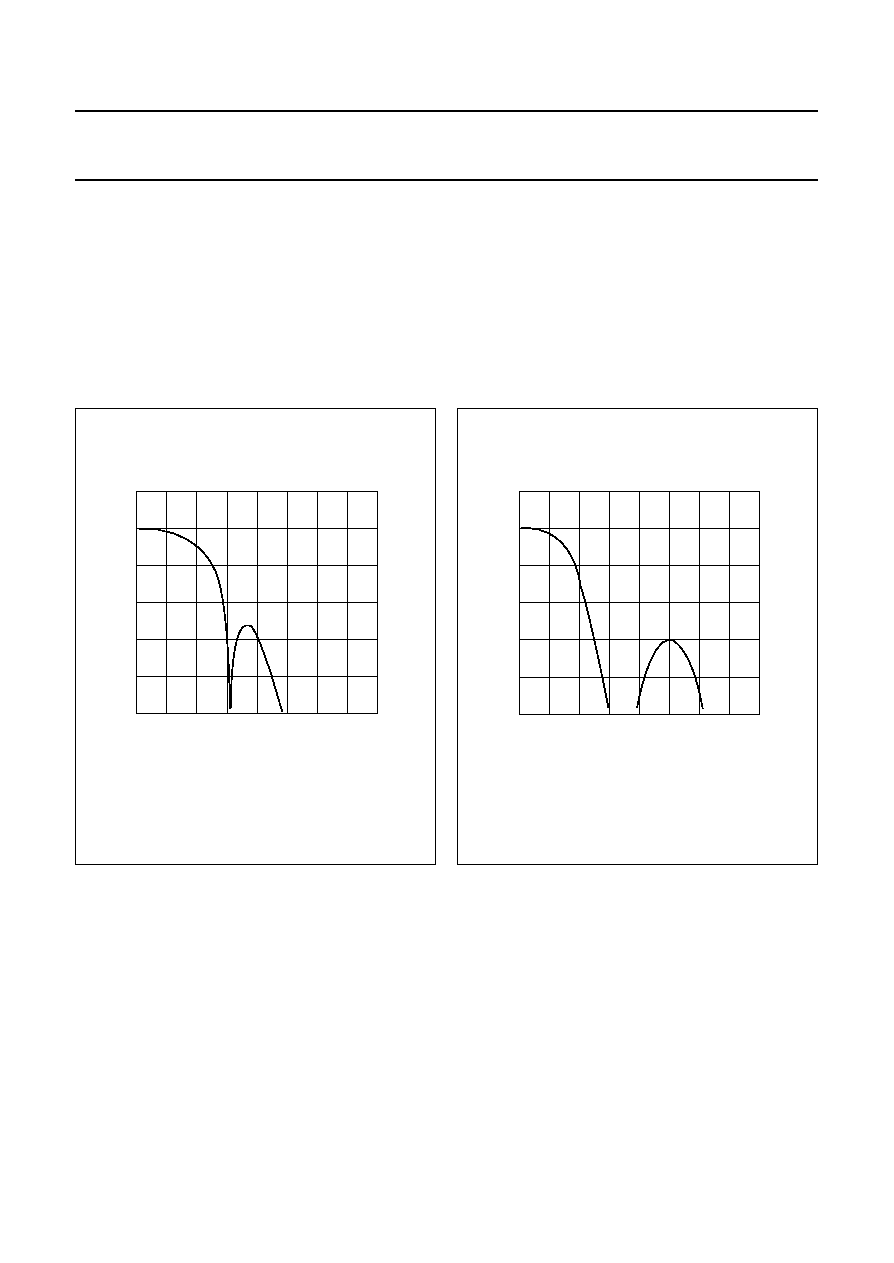
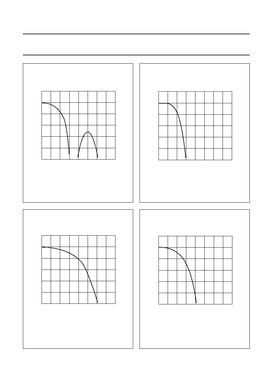
1. Decimation for 4 : 4 : 4 format input data (formats 4, 5 and 7; Fig.4).
2. Interpolation for 4 : 1 : 1 input data into 4 : 2 : 2 data, also suitable to reduce the bandwidth of 4 : 2 : 2 data. This filter
is controlled by the SCBW-bit (SCWB = 1 means active).
3. Interpolation at 13.5 MHz for 4 : 2 : 2 input data into 4 : 4 : 4 data before modulating baseband signals onto the
colour subcarrier. Figures 5, 6 and 7 show the overall transfer characteristics of chrominance in "standard bandwidth
condition" (SCBW = 1). Figures 8 and 9 show the overall transfer characteristics of chrominance in enhanced
bandwidth condition (SCBW = 0), which is not possible for 4 : 1 : 1 input data. The transfer curves are slightly
different at 12.27 and 14.75 MHz.
Fig.4
Transfer characteristics of
4 : 4 : 4 to 4 : 2 : 2 decimator.
handbook, halfpage
MEH346
0
0
-
10
-
20
-
30
-
40
-
50
f / fCLK
(dB)
10
0.2
0.4
0.6
0.8
Fig.5
Overall transfer characteristics 4 : 1 : 1
input data.
handbook, halfpage
MEH347
0
2
4
6
8
0
-
10
-
20
-
30
-
40
-
50
f (MHz)
(dB)
10
1996 Sep 27
23
Philips Semiconductors
Product specification
Digital Video Encoder (DENC)
GENLOCK-capable
SAA7199B
Fig.6
Overall transfer characteristics 4 : 2 : 2
input data (SCBW-bit = 1).
handbook, halfpage
MEH348
0
2
4
6
8
0
-
10
-
20
-
30
-
40
-
50
f (MHz)
(dB)
10
Fig.7
Overall transfer characteristics 4 : 4 : 4
input data (SCBW-bit = 1).
handbook, halfpage
MEH349
0
2
4
6
8
0
-
10
-
20
-
30
-
40
-
50
f (MHz)
(dB)
10
Fig.8
Overall transfer characteristics 4 : 2 : 2
input data (SCBW-bit = 0).
handbook, halfpage
MEH350
0
2
4
6
8
0
-
10
-
20
-
30
-
40
-
50
f (MHz)
(dB)
10
Fig.9
Overall transfer characteristics 4 : 4 : 4
input data (SCBW-bit = 0).
handbook, halfpage
MEH351
0
2
4
6
8
0
-
10
-
20
-
30
-
40
-
50
f (MHz)
(dB)
10

1996 Sep 27
24
Philips Semiconductors
Product specification
Digital Video Encoder (DENC)
GENLOCK-capable
SAA7199B
Accuracy of matrix
Evaluation of quantization errors.
The RGB to YUV matrix is achieved in accordance with
the following algorithm:
Y = INT
[(NINT(R
◊
2
◊
0.299) + NINT(G
◊
2
◊
0.587) + NINT(B
◊
2
◊
0.114) / 2]
U = NINT [(B
-
Y)
◊
0.57722]
V = NINT [(R
-
Y)
◊
0.72955].
Errors can occur in the calculation of Y, which as a result
influence the U and V outputs. The greatest positive error
occurs, if in all of the three for Y calculation used ROMs the
values are rounded up to 0.5 LSB, and no truncation error
of 0.5 LSB is generated after summation:
= +0.75 LSB;
with truncation "error":
-
0.5 LSB = +0.25 LSB.
The greatest negative error occurs at rounding off in all the
three ROMs and by consecutive truncation:
-
0.5 LSB =
-
1.25 LSB.
As a result, the matrix error can be
±
1 digit, which
corresponds to approximately
±
0.5% differential
non-linearity.
Estimation of noise by quantization
The sum of all sqared quantization errors is SS normalized
to 220
3
input combinations (3-dimensional colour scale).
SS = 0.187545 LSB
2
.
Compared with noise energy for ideal quantization,
SSI =
1
/
12
LSB
2
results in a deterioration by the conversion
matrix of:
D = 10 log (0.187545
◊
12) = 3.5 dB (equals 0.5 bit).
If SS is the sum of all squared quantization errors,
normalized to 220 input combinations of a grey-scale
(R = G = B), then:
SS = 0.12273 LSB
2
.
Compared with noise energy for ideal quantization,
SSI =
1
/
12
LSB
2
results in a deterioration by the conversion
matrix of:
D = 10 log (0.12273
◊
12) = 1.7 dB (equals 0.25 bit).
3
0.5 LSB
2
---------------------
◊
3
0.5 LSB
2
---------------------
◊
3
0.5 LSB
≠
2
------------------------
◊
Normalizing amplifiers in the luminance channel
The absolute amplification error for 50 Hz non-set-up
signals is 0.375%; differential non-linearity is
-
0.333%
(equals
-
1 LSB).
The absolute amplification error for 60 Hz set-up signals is
-
1.5%; differential non-linearity is
-
0.365%
(equals
-
1 LSB).
Normalizing amplifiers in the chrominance channel
The absolute amplification error is approximately
±
0.5%
with a truncation error of
-
0.5 LSB.
The subcarrier amplitude for standards with luminance
set-up is the same as for the standards without luminance
set-up.
Modulator
The absolute amplification error is
-
0.39%; there is no
truncation error.
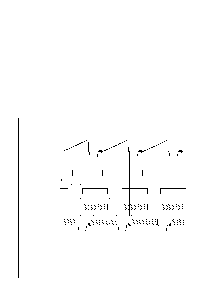
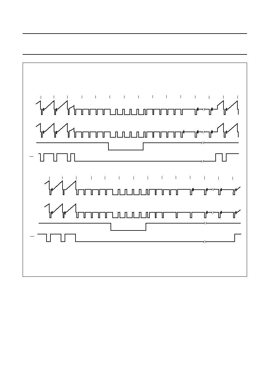
Functional timing (see Fig.10)
GENLOCK
MODE
The encoded signal can be generated earlier with respect
to CVBS7 to CVBS0 bits (offset t
ofs
set by GDC-bits;
index 05). The HSN output signal can be generated early
by PSO-bits (index 07) with respect to CB to compensate
for pipelining delay t
Rint
of the RAM interface (valid also in
stand alone mode).
The horizontal timing is independent of active video at data
inputs PDn(7 to 0). The line blanking period on the outputs
is set to approximately 12
µ
s in 50 Hz standards (11
µ
s in
60 Hz standards).
S
LAVE MODE
HSN pin is used as an input. The active edge of the input
signal is assumed to fit to the incoming CB signal.
Deviations can be compensated in the range of the
GCD-bits (index 05).
The t
enc
time is the total delay from data input to analog
CVBS output; it is 55 pixel clock periods long (PIXCLK)
plus the propagation delay of the LDV input register
regardless of mode and colour standard.
The key input signal is delay compensated with respect to
PDn(7 to 0) data input. The generated vertical field and
burst blanking sequences are shown in Fig.11 (50 Hz
PAL) and Fig.12 (60 Hz NTSC).
1996 Sep 27
25
Philips Semiconductors
Product specification
Digital Video Encoder (DENC)
GENLOCK-capable
SAA7199B
Reset
Prior to a reset all outputs are undefined. RESET = LOW
sets the circuit into the slave mode.
MOD1 bit = 1, MOD0-bit = 0. All other control register bits
are set to zero. The outputs CSYN/VSN, HSN, SLT, HSY
and HCL are automatically set to a high impedance
state.The I
2
C-bus interface is set to a slave receiver.
The D7 to D0 pins of the MPU interface are inputs during
RESET = LOW. As the circuit requires an external clock
signal on pin CLKIN in slave mode, the clock select signal
CLKSEL (pin 50) must be LOW during RESET = LOW
(pin 54). The LOW time of RESET is at least 50 pixel clock
periods long.
Disable chip
All analog outputs are set to zero by DD-bit = 1 (index 08);
while the outputs CSYN/VSN, HSN, HCL, HSY and SLT
are set to a high impedance state. The internal clock is
divided-by-4 at DD-bit = 1. The circuit can be disabled for
any reason and it must be disabled when CLKIN exceeds
32 MHz. After setting DD-bit = 1, the CLKIN input signal
can be set to a frequency of <60 MHz (modification of
control registers and RAM tables is not certain).
To re-enable the circuit, CLKIN must be set to a frequency
<32 MHz, a hardware reset is then required to set DD-bit
to zero.
Fig.10 Horizontal timing.
(1) t
Rint
is the pipeline delay of the RAM interface adjustable from
-
5 to +58 pixel clocks (PIXCLK).
(2)
t = 125
◊
PIXCLK at 12.27 MHz
t = 163
◊
PIXCLK at 14.75 MHz
t = 134
◊
PIXCLK at 13.50 MHz in 50 Hz mode
t = 122
◊
PIXCLK at 13.50 MHz in 60 Hz mode.
(3) t
ofs
is the propagation delay of external GENLOCK line adjustable from
-
17 to +46 pixel clocks.
handbook, full pagewidth
MEH345-1
CVBS input signal;
GENLOCK only
tREF2
tREF1
tRint
(1)
tenc
tofs
(3)
HSN output signal
CB input signal
PDn(7 to 0)
digital input data
CVBS output signal
t
(2)
active video
0 to 640/720/780
PIXCLK
1996 Sep 27
26
Philips Semiconductors
Product specification
Digital Video Encoder (DENC)
GENLOCK-capable
SAA7199B
Fig.11 Vertical field and burst blanking sequence for PAL 50 Hz mode.
handbook, full pagewidth
MEH352-1
(a) 1st field CVBS output signal
VSN
25
CB
24
23
7
6
5
4
3
2
1
625
624
623
622
621
VSN
CB
336
335
320
319
318
317
316
315
314
313
312
311
310
309
(a) 3rd field CVBS output signal
(b) 2nd field CVBS output signal
(b) 4th field CVBS output signal

1996 Sep 27
27
Philips Semiconductors
Product specification
Digital Video Encoder (DENC)
GENLOCK-capable
SAA7199B
Fig.12 Vertical field and burst blanking sequence for NTSC 60 Hz mode.
handbook, full pagewidth
MEH353-1
(a) 1st field CVBS output signal
VSN
21
CB
20
19
7
6
5
4
3
2
1
525
524
523
522
521
VSN
CB
282
281
270
269
268
267
266
265
264
263
262
261
260
259
(b) 2nd field CVBS output signal

1996 Sep 27
28
Philips Semiconductors
Product specification
Digital Video Encoder (DENC)
GENLOCK-capable
SAA7199B
LIMITING VALUES
In accordance with the Absolute Maximum Rating System (IEC 134).
Note
1. Equivalent to discharging a 100 pF capacitor through a 1.5 k
series resistor.
SYMBOL
PARAMETER
CONDITIONS
MIN.
MAX.
UNIT
V
DDA1
analog supply voltage 1 (pin 66)
-
0.3
+7
V
V
DDA2
analog supply voltage 2 (pin 70)
-
0.3
+7
V
V
DDA3
analog supply voltage 3 (pin 72)
-
0.3
+7
V
V
DDA4
analog supply voltage 4 (pin 64)
-
0.3
+7
V
V
DDD1
digital supply voltage 1 (pin 2)
-
0.3
+7
V
V
DDD2
digital supply voltage 2 (pin 21)
-
0.3
+7
V
V
DDD3
digital supply voltage 3 (pin 41)
-
0.3
+7
V
V
diff(GND)
voltage difference between analog and digital ground pins
(V
SSA
-
V
SSDn
)
-
±
100
mV
V
n
voltage on all pins except grounds
0
V
P
V
P
tot
total power dissipation
-
1.1
W
T
stg
storage temperature
-
65
+150
∞
C
T
amb
operating ambient temperature
0
70
∞
C
V
esd
electrostatic handling for all pins
note 1
-
2000
+2000
V
1996 Sep 27
29
Philips Semiconductors
Product specification
Digital Video Encoder (DENC)
GENLOCK-capable
SAA7199B
CHARACTERISTICS
V
DDA
= 4.75 to 5.25 V; V
DDD
= 4.5 to 5.5 V; T
amb
= 0 to 70
∞
C; unless otherwise specified.
SYMBOL
PARAMETER
CONDITIONS
MIN.
TYP.
MAX.
UNIT
V
DDA
analog supply voltage
(pins 64, 66, 70 and 72)
4.75
5.0
5.25
V
V
DDD
digital supply voltage (pins 2, 21 and 41)
4.5
5.0
5.5
V
I
DDA
analog supply current I
DDA1
to I
DDA4
40 pF output load
-
-
60
mA
I
DDD
digital supply current I
DDD1
to I
DDD3
40 pF output load
-
-
140
mA
Data and control inputs (pins 3 to 20, 23 to 40, 43 to 46, 49, 50, 54 to 56, 59, 73 and 76 to 84)
V
IL
LOW level input voltage
note 1
0
-
0.8
V
V
IH
HIGH level input voltage
note 1
2.0
-
V
DDD
+ 0.5 V
I
LI
input leakage current
-
1
-
+1
µ
A
C
i
input capacitance
data inputs
-
-
8
pF
CLKIN, LLC and LDV
-
-
10
pF
3-state I/O
-
-
10
pF
LFCO output (pin 61)
V
o(p-p)
output voltage (peak-to-peak value)
1.4
-
2.6
V
V
61
output voltage range
0
-
V
DDD
V
Data and other control outputs (pins 3, 51, 52, 57, 58, 60, 74 and 75)
V
OL
LOW level output voltage
note 2
0
-
0.6
V
V
OH
HIGH level output voltage
note 2
2.4
-
V
DDD
V
C, Y and CVBS analog outputs (pins 65, 67 and 69)
V
o(p-p)
output voltage (peak-to-peak value)
without load; V
DDA
= 5 V
-
2
-
V
V
o(min)
minimum output voltage
without load; V
DDA
= 5 V
-
0.2
-
V
V
o(max)
maximum output voltage
without load; V
DDA
= 5 V
-
2.2
-
V
R
o(int)
internal serial output resistance
not tested
18
25
35
R
L
output load resistance
recommendation
90
-
-
B
output signal bandwidth
-
3 dB
10
-
-
MHz
ILE
LF integral linearity error
9-bit data
-
-
±
1.0
LSB
DLE
LF differential linearity error
9-bit data
-
-
±
0.5
LSB
I
CUR
input current (pin 71)
Fig.1; R
70-71
= 20 k
-
300
-
µ
A
I
2
C-bus SDA and SCL (pins 47 and 48)
V
IL
LOW level input voltage
-
0.5
-
+1.5
V
V
IH
HIGH level input voltage
3.0
-
V
DDD
+ 0.5 V
I
I
input current
V
I
= LOW or HIGH
-
10
-
+10
µ
A
V
OL
SDA LOW level output voltage
I
OL
= 3 mA
-
-
0.4
V
I
O
SDA output current
during acknowledge
3
-
-
mA

1996 Sep 27
30
Philips Semiconductors
Product specification
Digital Video Encoder (DENC)
GENLOCK-capable
SAA7199B
Crystal oscillator (see Fig.15)
f
n
nominal frequency
3rd harmonic; Table 1
-
24.576
-
MHz
3rd harmonic; Table 1
-
26.8
-
MHz
f/f
n
permissible deviation of f
n
-
50
-
10
-
6
X1 crystal specification
T
amb
ambient temperature range
0
-
70
∞
C
C
L
load capacitance
8
-
-
pF
R
s
series resonance resistance
-
40
80
C
mot
motional capacitance
-
20%
1.5
+20%
fF
C
par
parallel capacitance
-
20%
3.5
+20%
pF
LDV and LLC timing (pins 20 and 55) see Fig.17
T
cy(LLC)
LLC cycle time
note 3
31.5
-
44.5
ns
t
W(CH)
pulse width
40
50
60
%
t
r
rise time
-
-
5
ns
t
f
fall time
-
-
6
ns
t
cy(LDV)
LDV cycle time
63
-
89
ns
t
su(LDV)
LDV set-up time
4
-
-
ns
t
h(LDV)
LDV hold time
10
-
-
ns
PIXCLK and CLKO timing (pins 51 and 52) see Fig.17
t
d(CLK)
PIXCLK and CLKO delay time
-
-
25
ns
PD1 to 3(7 to 0), CB, MPK, KEY and RTCI input timing (pins 4 to 19, 23 to 32, 57 and 73) see Fig.17
t
SU; DAT
input data set-up time
4
-
-
ns
t
HD; DAT
input data hold time
6
-
-
ns
CVBS(7 to 0), VSN/CSYN and HSN timing (pins 76 to 83, 3 and 84) see Fig.18
t
SU; DAT
input data set-up time
10
-
-
ns
t
HD; DAT
input data hold time
5
-
-
ns
CREF timing (pin 56) see Fig.18
t
SU(CREF)
input set-up time
10
-
-
ns
t
h(CREF)
input hold time
2
-
-
ns
SYMBOL
PARAMETER
CONDITIONS
MIN.
TYP.
MAX.
UNIT
1996 Sep 27
31
Philips Semiconductors
Product specification
Digital Video Encoder (DENC)
GENLOCK-capable
SAA7199B
Notes
1. XTALO, XTALI and TP are not characterized with respect to levels; CLKO is characterized up to 32 MHz and PIXCLK
up to 16 MHz.
2. Levels are measured with load circuit. LFCO output with 10 k
in parallel with 15 pF and other outputs with 1.2 k
in parallel with 40 pF at 3 V (TTL load).
3. T
LLC
must be 63 to 89 ns at CREF = HIGH (pin 56); T
LLC
= 16.5 ns is only allowed if the multiplexer clock is active.
4. t
PIXCLK(min)
+ 5 ns.
5. 3
◊
[t
PIXCLK(min)
+ 5 ns].
6. 40 ns at low supply voltage (4 V) and high temperature (70
∞
C).
MPU timing A1, A0, R/W, CS, D(7 to 0) (pins 33 to 36, 37 to 40 and 43 to 46) see Fig.19
t
su(ADD)
A1 and A0 address set-up time
(pins 33 and 34)
4
-
-
ns
t
h(ADD)
A1 and A0 address hold time
25
-
-
ns
t
su(R)
R/W set-up time (pin 35)
4
-
-
ns
t
h(R)
R/W hold time
25
-
-
ns
t
W(CL)
CS pulse width LOW
note 4
95
-
-
ns
t
W(CH)
CS pulse width HIGH
note 4
95
-
-
ns
t
su;DAT
data set-up time (D7 to D0)
write mode
80
-
-
ns
t
h;DAT
data hold time (D7 to D0)
write mode
5
-
-
ns
t
d(Q)
data output hold time (D7 to D0)
read mode
5
-
-
ns
t
ZR
delay to driven ports (D7 to D0)
read mode
5
-
-
ns
t
d(ZR)
delay to ports valid (D7 to D0)
read mode; note 5
-
-
275
ns
t
d(RZ)
port outputs disable time (D7 to D0)
read mode
-
-
25
ns
Output timing (pins 3, 74, 75 and 84); see Fig.18
t
d
output delay time
minimum clock period;
note 6
-
20
45
ns
SYMBOL
PARAMETER
CONDITIONS
MIN.
TYP.
MAX.
UNIT
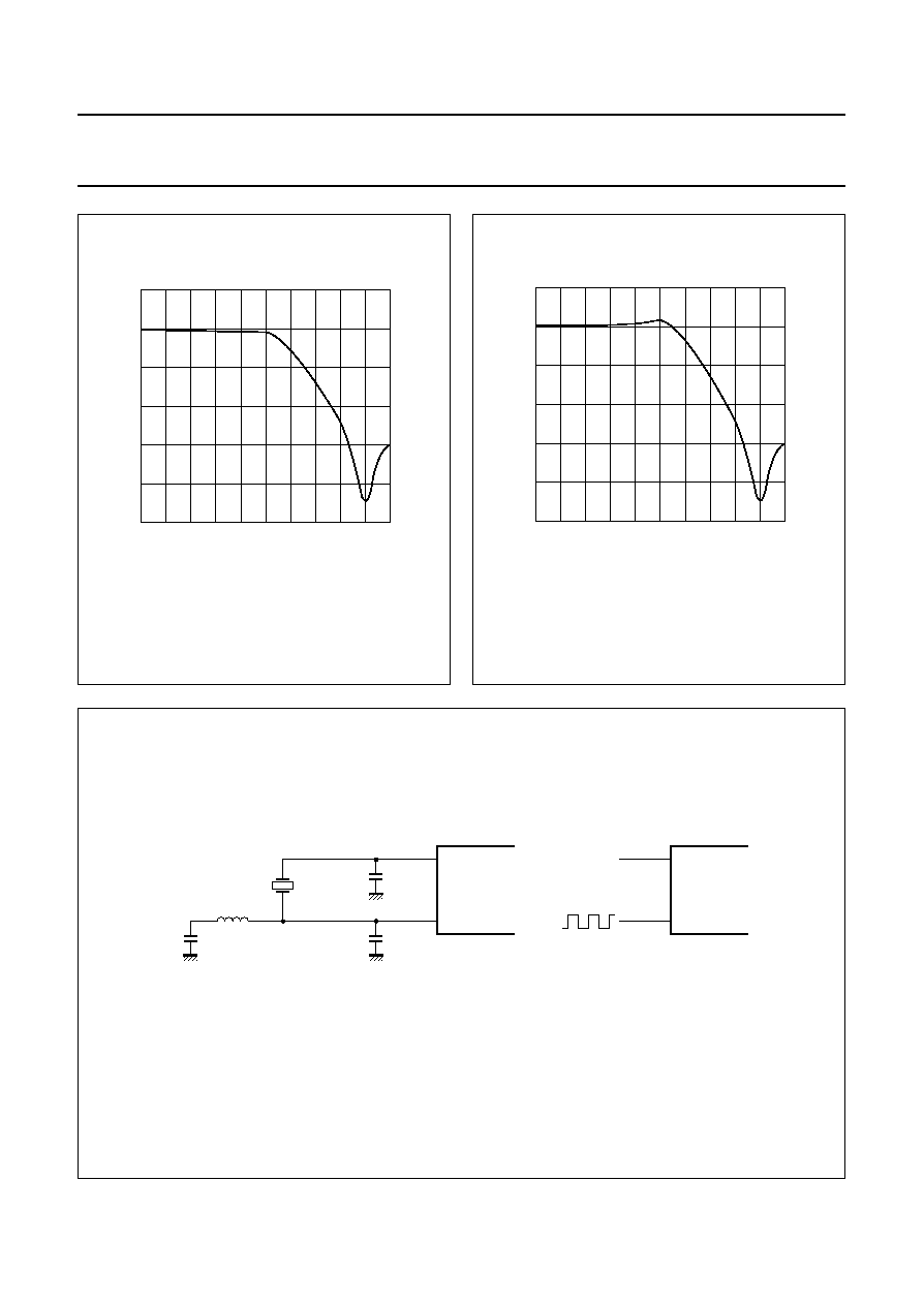
1996 Sep 27
32
Philips Semiconductors
Product specification
Digital Video Encoder (DENC)
GENLOCK-capable
SAA7199B
Fig.13 Characteristics of low-pass post-filters;
without compensation of DC hold.
handbook, halfpage
MEH357
0
2
4
6
8
0
-
10
-
20
-
30
-
40
-
50
f (MHz)
(dB)
10
10
Fig.14 Characteristics of low-pass post-filters.;
with compensation of DC hold.
handbook, halfpage
MEH358
0
2
4
6
8
0
-
10
-
20
-
30
-
40
-
50
f (MHz)
(dB)
10
10
Fig.15 Oscillator application (a) and optional external clock sync (b).
(1) Value depends on crystal parameters.
(2) 24.576 MHz (3rd harmonic), Philips: 4322 143 05291; 26.8 MHz (3rd harmonic), Philips: 9922 520 30004.
handbook, full pagewidth
SAA7199B
60
59
10 pF
XTALI
XTALO
SAA7199B
60
59
XTALI
XTALO
10 pF
1 nF
MHA417
10
µ
H
±
20 %
(1)
(2)
(1)
X1
(a)
(b)

1996 Sep 27
33
Philips Semiconductors
Product specification
Digital Video Encoder (DENC)
GENLOCK-capable
SAA7199B
agewidth
MEH420
SAA7199B
66
70
72
CUR
+
5 V
71
20 k
64
63
41
+
5 V
21
2
digital input
and output
signals
of Fig.1
external output filters
68
69
CVBS
67
Y
65
C
62
1
22
42
V
SSD1
V
SSD3
V
refL
V
SSD2
V
SSA
0.1
µ
F
0.1
µ
F
0.1
µ
F
0.1
µ
F
0.1
µ
F
0.1
µ
F
0.1
µ
F
0.1
µ
F
0.1
µ
F
V
DDD1
V
DDD2
V
DDD3
V
DDA4
V
refH
V
DDA1
V
DDA2
V
DDA3
25
22
(3)
75
(3)
1.23 V (p-p)
DAC2
25
22
(3)
75
(3)
1.23 V (p-p)
DAC3
25
22
(3)
75
(3)
1.23 V (p-p)
DAC1
20 k
390 pF
560 pF
120 pF
2.7
µ
H
1.8
µ
H
25
22
(3)
75
(3)
1.23 V (p-p)
analog
output
1.23 V (p-p)
analog
output
load
(2)
390 pF
560 pF
120 pF
2.7
µ
H
2.7
µ
H
25
22
(3)
75
(3)
load
(1)
Fig.16 Application details of Fig.1 showing proposals of analog low-pass post-filtering of output signals.
(1)
Without compensation of the DAC hold characteristic (see Fig.13).
(2)
With compensation of the DAC hold characteristic
correction (see Fig.14).
(3)
Output amplitude determined by load resistors R
L
>9
0
.
x
()
sin
x
-----------------
-
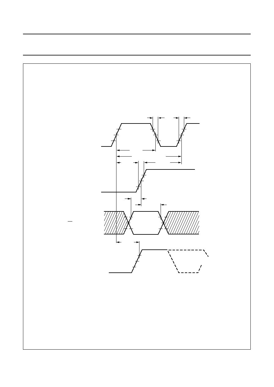
1996 Sep 27
34
Philips Semiconductors
Product specification
Digital Video Encoder (DENC)
GENLOCK-capable
SAA7199B
Fig.17 LDV input data timing.
handbook, full pagewidth
MEH421
tsu(LDV)
th(LDV)
tw(CH)
Tcy(LLC); Tcy(CLKIN)
2.0 V
1.5 V
0.8 V
2.0 V
0.8 V
2.0 V
1.5 V
0.8 V
tSU; DAT
tHD; DAT
tf
tr
td(CLK)
data valid
input clocks
LLC and CLKIN
input data clock
LDV
inputdata PDn(7 to 0)
CB, MPK, KEY
and RTCI (pin 57)
CLKO and
PIXCLK
PIXCLK
CLKO
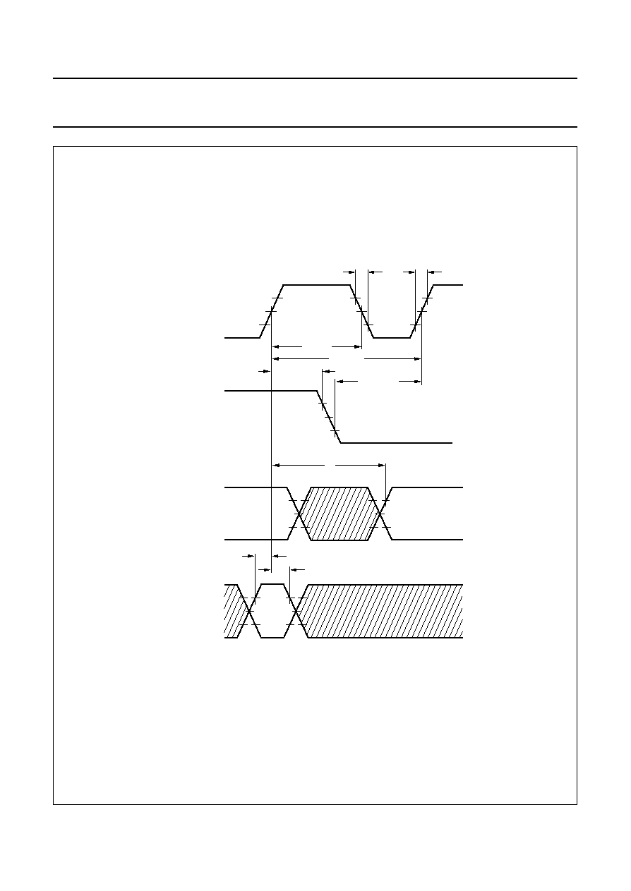
1996 Sep 27
35
Philips Semiconductors
Product specification
Digital Video Encoder (DENC)
GENLOCK-capable
SAA7199B
Fig.18 Clock and data timing.
handbook, full pagewidth
MEH355
tsu(CREF)
th(CREF)
tw(CH)
Tcy(LLC)
2.0 V
1.5 V
0.8 V
2.4 V
0.6 V
2.0 V
2.0 V
1.5 V
0.8 V
tSU; DAT
tHD; DAT
tf
tr
td
data valid
data valid
data valid
0.8 V
input clock LLC
input CREF
outputs
HCL, HSY, HSN,
VSN and CSYN
input data
CVBS(7 to 0)

1996 Sep 27
36
Philips Semiconductors
Product specification
Digital Video Encoder (DENC)
GENLOCK-capable
SAA7199B
Fig.19 MPU-bus timing.
handbook, full pagewidth
MEH356
tW(CL)
input CS
inputs
A1 and A0
input R/W
write D
(7 to 0)
read D
(7 to 0)
th(ADD)
tsu(ADD)
th(R)
1.5 V
1.5 V
data valid
1.5 V
data valid
data valid
1.5 V
tsu(R)
tW(CH)
2.0 V
1.5 V
0.8 V
th;DAT
tsu;DAT
td(Q)
td(RZ)
td(DR)
td(ZR)
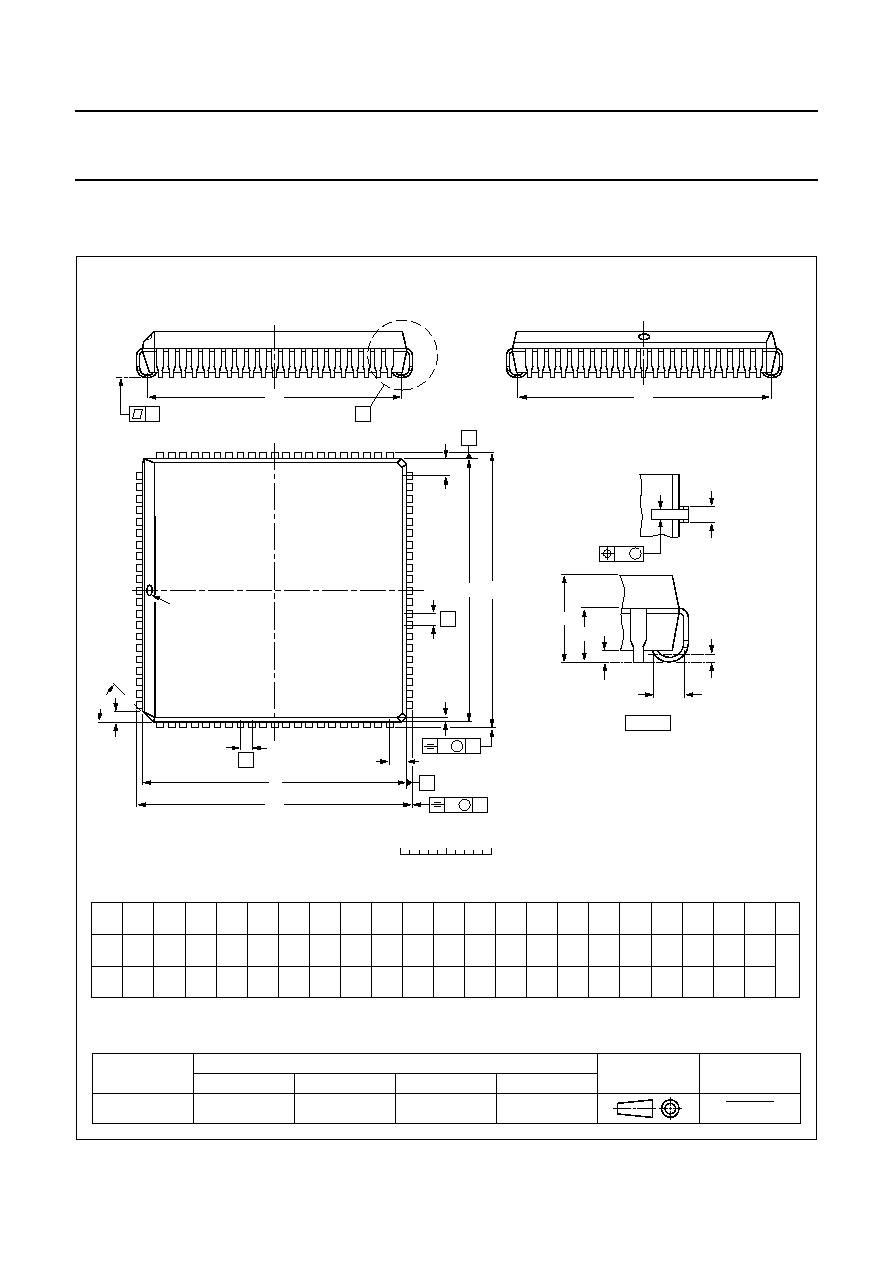
1996 Sep 27
37
Philips Semiconductors
Product specification
Digital Video Encoder (DENC)
GENLOCK-capable
SAA7199B
PACKAGE OUTLINE
REFERENCES
OUTLINE
VERSION
EUROPEAN
PROJECTION
ISSUE DATE
IEC
JEDEC
EIAJ
Note
1. Plastic or metal protrusions of 0.01 inches maximum per side are not included.
SOT189-2
54
74
84
1
11
12
32
53
33
75
detail X
(A )
3
b
p
w
M
A
1
A
A
4
L
p
b
1
k
1
k
X
y
e
E
B
D
H
E
H
v
M
B
D
Z D
A
Z E
e
v
M
A
pin 1 index
0
5
10 mm
scale
92-11-17
95-03-11
PLCC84: plastic leaded chip carrier; 84 leads
SOT189-2
UNIT
A
A
min.
max.
max.
max. max.
1
A
4
b
p
E
(1)
(1)
(1)
e
H
E
Z
y
w
v
mm
4.57
4.19
0.51
3.30
0.53
0.33
0.021
0.013
1.27
0.51
2.16
45
o
0.18
0.10
0.18
DIMENSIONS (millimetre dimensions are derived from the original inch dimensions)
D
(1)
29.41
29.21
H
D
30.35
30.10
E
Z
2.16
D
b
1
0.81
0.66
k
1.22
1.07
k
1
0.180
0.165
0.020
0.13
A
3
0.25
0.01
0.05
0.020
0.085
0.007 0.004
0.007
L
p
1.44
1.02
0.057
0.040
1.158
1.150
29.41
29.21
1.158
1.150
1.195
1.185
30.35
30.10
1.195
1.185
e
E
e
D
28.70
27.69
1.130
1.090
28.70
27.69
1.130
1.090
0.085
0.032
0.026
0.048
0.042
E
e
inches
D
e

1996 Sep 27
38
Philips Semiconductors
Product specification
Digital Video Encoder (DENC)
GENLOCK-capable
SAA7199B
SOLDERING
Introduction
There is no soldering method that is ideal for all IC
packages. Wave soldering is often preferred when
through-hole and surface mounted components are mixed
on one printed-circuit board. However, wave soldering is
not always suitable for surface mounted ICs, or for
printed-circuits with high population densities. In these
situations reflow soldering is often used.
This text gives a very brief insight to a complex technology.
A more in-depth account of soldering ICs can be found in
our
"IC Package Databook" (order code 9398 652 90011).
Reflow soldering
Reflow soldering techniques are suitable for all PLCC
packages.
The choice of heating method may be influenced by larger
PLCC packages (44 leads, or more). If infrared or vapour
phase heating is used and the large packages are not
absolutely dry (less than 0.1% moisture content by
weight), vaporization of the small amount of moisture in
them can cause cracking of the plastic body. For more
information, refer to the Drypack chapter in our
"Quality
Reference Handbook" (order code 9397 750 00192).
Reflow soldering requires solder paste (a suspension of
fine solder particles, flux and binding agent) to be applied
to the printed-circuit board by screen printing, stencilling or
pressure-syringe dispensing before package placement.
Several techniques exist for reflowing; for example,
thermal conduction by heated belt. Dwell times vary
between 50 and 300 seconds depending on heating
method. Typical reflow temperatures range from
215 to 250
∞
C.
Preheating is necessary to dry the paste and evaporate
the binding agent. Preheating duration: 45 minutes at
45
∞
C.
Wave soldering
Wave soldering techniques can be used for all PLCC
packages if the following conditions are observed:
∑
A double-wave (a turbulent wave with high upward
pressure followed by a smooth laminar wave) soldering
technique should be used.
∑
The longitudinal axis of the package footprint must be
parallel to the solder flow.
∑
The package footprint must incorporate solder thieves at
the downstream corners.
During placement and before soldering, the package must
be fixed with a droplet of adhesive. The adhesive can be
applied by screen printing, pin transfer or syringe
dispensing. The package can be soldered after the
adhesive is cured.
Maximum permissible solder temperature is 260
∞
C, and
maximum duration of package immersion in solder is
10 seconds, if cooled to less than 150
∞
C within
6 seconds. Typical dwell time is 4 seconds at 250
∞
C.
A mildly-activated flux will eliminate the need for removal
of corrosive residues in most applications.
Repairing soldered joints
Fix the component by first soldering two diagonally-
opposite end leads. Use only a low voltage soldering iron
(less than 24 V) applied to the flat part of the lead. Contact
time must be limited to 10 seconds at up to 300
∞
C. When
using a dedicated tool, all other leads can be soldered in
one operation within 2 to 5 seconds between
270 and 320
∞
C.
1996 Sep 27
39
Philips Semiconductors
Product specification
Digital Video Encoder (DENC)
GENLOCK-capable
SAA7199B
DEFINITIONS
LIFE SUPPORT APPLICATIONS
These products are not designed for use in life support appliances, devices, or systems where malfunction of these
products can reasonably be expected to result in personal injury. Philips customers using or selling these products for
use in such applications do so at their own risk and agree to fully indemnify Philips for any damages resulting from such
improper use or sale.
PURCHASE OF PHILIPS I
2
C COMPONENTS
Data sheet status
Objective specification
This data sheet contains target or goal specifications for product development.
Preliminary specification
This data sheet contains preliminary data; supplementary data may be published later.
Product specification
This data sheet contains final product specifications.
Limiting values
Limiting values given are in accordance with the Absolute Maximum Rating System (IEC 134). Stress above one or
more of the limiting values may cause permanent damage to the device. These are stress ratings only and operation
of the device at these or at any other conditions above those given in the Characteristics sections of the specification
is not implied. Exposure to limiting values for extended periods may affect device reliability.
Application information
Where application information is given, it is advisory and does not form part of the specification.
Purchase of Philips I
2
C components conveys a license under the Philips' I
2
C patent to use the
components in the I
2
C system provided the system conforms to the I
2
C specification defined by
Philips. This specification can be ordered using the code 9398 393 40011.

Internet: http://www.semiconductors.philips.com
Philips Semiconductors ≠ a worldwide company
© Philips Electronics N.V. 1996
SCA51
All rights are reserved. Reproduction in whole or in part is prohibited without the prior written consent of the copyright owner.
The information presented in this document does not form part of any quotation or contract, is believed to be accurate and reliable and may be changed
without notice. No liability will be accepted by the publisher for any consequence of its use. Publication thereof does not convey nor imply any license
under patent- or other industrial or intellectual property rights.
Netherlands: Postbus 90050, 5600 PB EINDHOVEN, Bldg. VB,
Tel. +31 40 27 82785, Fax. +31 40 27 88399
New Zealand: 2 Wagener Place, C.P.O. Box 1041, AUCKLAND,
Tel. +64 9 849 4160, Fax. +64 9 849 7811
Norway: Box 1, Manglerud 0612, OSLO,
Tel. +47 22 74 8000, Fax. +47 22 74 8341
Philippines: Philips Semiconductors Philippines Inc.,
106 Valero St. Salcedo Village, P.O. Box 2108 MCC, MAKATI,
Metro MANILA, Tel. +63 2 816 6380, Fax. +63 2 817 3474
Poland: Ul. Lukiska 10, PL 04-123 WARSZAWA,
Tel. +48 22 612 2831, Fax. +48 22 612 2327
Portugal: see Spain
Romania: see Italy
Russia: Philips Russia, Ul. Usatcheva 35A, 119048 MOSCOW,
Tel. +7 095 926 5361, Fax. +7 095 564 8323
Singapore: Lorong 1, Toa Payoh, SINGAPORE 1231,
Tel. +65 350 2538, Fax. +65 251 6500
Slovakia: see Austria
Slovenia: see Italy
South Africa: S.A. PHILIPS Pty Ltd., 195-215 Main Road Martindale,
2092 JOHANNESBURG, P.O. Box 7430 Johannesburg 2000,
Tel. +27 11 470 5911, Fax. +27 11 470 5494
South America: Rua do Rocio 220, 5th floor, Suite 51,
04552-903 S„o Paulo, S√O PAULO - SP, Brazil,
Tel. +55 11 821 2333, Fax. +55 11 829 1849
Spain: Balmes 22, 08007 BARCELONA,
Tel. +34 3 301 6312, Fax. +34 3 301 4107
Sweden: Kottbygatan 7, Akalla, S-16485 STOCKHOLM,
Tel. +46 8 632 2000, Fax. +46 8 632 2745
Switzerland: Allmendstrasse 140, CH-8027 ZÐRICH,
Tel. +41 1 488 2686, Fax. +41 1 481 7730
Taiwan: PHILIPS TAIWAN Ltd., 23-30F, 66,
Chung Hsiao West Road, Sec. 1, P.O. Box 22978,
TAIPEI 100, Tel. +886 2 382 4443, Fax. +886 2 382 4444
Thailand: PHILIPS ELECTRONICS (THAILAND) Ltd.,
209/2 Sanpavuth-Bangna Road Prakanong, BANGKOK 10260,
Tel. +66 2 745 4090, Fax. +66 2 398 0793
Turkey: Talatpasa Cad. No. 5, 80640 GÐLTEPE/ISTANBUL,
Tel. +90 212 279 2770, Fax. +90 212 282 6707
Ukraine: PHILIPS UKRAINE, 4 Patrice Lumumba str., Building B, Floor 7,
252042 KIEV, Tel. +380 44 264 2776, Fax. +380 44 268 0461
United Kingdom: Philips Semiconductors Ltd., 276 Bath Road, Hayes,
MIDDLESEX UB3 5BX, Tel. +44 181 730 5000, Fax. +44 181 754 8421
United States: 811 East Arques Avenue, SUNNYVALE, CA 94088-3409,
Tel. +1 800 234 7381
Uruguay: see South America
Vietnam: see Singapore
Yugoslavia: PHILIPS, Trg N. Pasica 5/v, 11000 BEOGRAD,
Tel. +381 11 825 344, Fax.+381 11 635 777
For all other countries apply to: Philips Semiconductors, Marketing & Sales Communications,
Building BE-p, P.O. Box 218, 5600 MD EINDHOVEN, The Netherlands, Fax. +31 40 27 24825
Argentina: see South America
Australia: 34 Waterloo Road, NORTH RYDE, NSW 2113,
Tel. +61 2 9805 4455, Fax. +61 2 9805 4466
Austria: Computerstr. 6, A-1101 WIEN, P.O. Box 213,
Tel. +43 1 60 101, Fax. +43 1 60 101 1210
Belarus: Hotel Minsk Business Center, Bld. 3, r. 1211, Volodarski Str. 6,
220050 MINSK, Tel. +375 172 200 733, Fax. +375 172 200 773
Belgium: see The Netherlands
Brazil: see South America
Bulgaria: Philips Bulgaria Ltd., Energoproject, 15th floor,
51 James Bourchier Blvd., 1407 SOFIA,
Tel. +359 2 689 211, Fax. +359 2 689 102
Canada: PHILIPS SEMICONDUCTORS/COMPONENTS,
Tel. +1 800 234 7381
China/Hong Kong: 501 Hong Kong Industrial Technology Centre,
72 Tat Chee Avenue, Kowloon Tong, HONG KONG,
Tel. +852 2319 7888, Fax. +852 2319 7700
Colombia: see South America
Czech Republic: see Austria
Denmark: Prags Boulevard 80, PB 1919, DK-2300 COPENHAGEN S,
Tel. +45 32 88 2636, Fax. +45 31 57 1949
Finland: Sinikalliontie 3, FIN-02630 ESPOO,
Tel. +358 615 800, Fax. +358 615 80920
France: 4 Rue du Port-aux-Vins, BP317, 92156 SURESNES Cedex,
Tel. +33 1 40 99 6161, Fax. +33 1 40 99 6427
Germany: Hammerbrookstraþe 69, D-20097 HAMBURG,
Tel. +49 40 23 53 60, Fax. +49 40 23 536 300
Greece: No. 15, 25th March Street, GR 17778 TAVROS,
Tel. +30 1 4894 339/911, Fax. +30 1 4814 240
Hungary: see Austria
India: Philips INDIA Ltd, Shivsagar Estate, A Block, Dr. Annie Besant Rd.
Worli, MUMBAI 400 018, Tel. +91 22 4938 541, Fax. +91 22 4938 722
Indonesia: see Singapore
Ireland: Newstead, Clonskeagh, DUBLIN 14,
Tel. +353 1 7640 000, Fax. +353 1 7640 200
Israel: RAPAC Electronics, 7 Kehilat Saloniki St, TEL AVIV 61180,
Tel. +972 3 645 0444, Fax. +972 3 649 1007
Italy: PHILIPS SEMICONDUCTORS, Piazza IV Novembre 3,
20124 MILANO, Tel. +39 2 6752 2531, Fax. +39 2 6752 2557
Japan: Philips Bldg 13-37, Kohnan 2-chome, Minato-ku, TOKYO 108,
Tel. +81 3 3740 5130, Fax. +81 3 3740 5077
Korea: Philips House, 260-199 Itaewon-dong, Yongsan-ku, SEOUL,
Tel. +82 2 709 1412, Fax. +82 2 709 1415
Malaysia: No. 76 Jalan Universiti, 46200 PETALING JAYA, SELANGOR,
Tel. +60 3 750 5214, Fax. +60 3 757 4880
Mexico: 5900 Gateway East, Suite 200, EL PASO, TEXAS 79905,
Tel. +9-5 800 234 7381
Middle East: see Italy
Printed in The Netherlands
657021/1200/02/pp40
Date of release: 1996 Sep 27
Document order number:
9397 750 01285