 | –≠–ª–µ–∫—Ç—Ä–æ–Ω–Ω—ã–π –∫–æ–º–ø–æ–Ω–µ–Ω—Ç: SAA7346 | –°–∫–∞—á–∞—Ç—å:  PDF PDF  ZIP ZIP |
Document Outline
- FEATURES
- GENERAL DESCRIPTION
- QUICK REFERENCE DATA
- ORDERING INFORMATION
- BLOCK DIAGRAM
- PINNING
- FUNCTIONAL DESCRIPTION
- I 2 S input/output interfaces
- New subcode frame regeneration
- Shock processor
- FIFO controller and monitor
- Microcontroller interface
- DRAM interface
- System clock
- Reset
- Kill interface
- Read cycle divide (RCD2)
- LIMITING VALUES
- THERMAL CHARACTERISTICS
- CHARACTERISTICS
- APPLICATION INFORMATION
- PACKAGE OUTLINE
- SOLDERING
- DEFINITIONS
- LIFE SUPPORT APPLICATIONS

DATA SHEET
Preliminary specification
File under Integrated Circuits, IC01
July 1994
INTEGRATED CIRCUITS
Philips Semiconductors
SAA7346
Shock absorbing RAM addresser
July 1994
2
Philips Semiconductors
Preliminary specification
Shock absorbing RAM addresser
SAA7346
FEATURES
∑
Absorbs shocks from x, y and z directions
∑
Absorbs rotational shocks
∑
Absorbs multiple shocks per second
∑
Interfaces directly to compact disc decoders SAA7345,
SAA7347 and SAA7370
∑
Multi-speed I
2
S-bus input with single-speed
I
2
S-bus output
∑
Controls 1 or 4 MBit of external Dynamic Random
Access Memory (DRAM)
∑
Easy serial interface for communication with common
microcontrollers
∑
Software selectable shock detectors
∑
By-pass/power-down mode
∑
Kill interface for DAC deactivation
∑
Can be used for:
≠ `sampling' part of a disc
≠ to reduce access pauses between jumps
≠ to deliver a programmable delay
≠ to generate a fixed audio rate from Constant Angular
Velocity (CAV) discs.
GENERAL DESCRIPTION
The SAA7346 can be used to make a CD player
insensitive to shocks. To do this, SAA7346 operates
closely with a standard 1 Mbit or 4 Mbit DRAM. Audio data
is stored inside the DRAM and during shocks the data of
the DRAM can be played. The SAA7346 functions as a
customized DRAM controller with serial I/O and on-board
shock detectors.
QUICK REFERENCE DATA
ORDERING INFORMATION
Note
1. When using reflow soldering it is recommended that the Dry Packing instructions in the
"Quality Reference
Pocketbook" are followed. The pocketbook can be ordered using the code 9398 510 34011.
SYMBOL
PARAMETER
MIN.
TYP.
MAX.
UNIT
V
DD
supply voltage
3.3
5.0
5.5
V
I
DD
supply current
-
12
-
mA
f
clk
clock frequency
-
16.9344
-
MHz
f
i(clk)
I
2
S input word clock frequency
44.1
88.2
176.4
kHz
f
o(clk)
I
2
S output word clock frequency
44.1
88.2
176.4
kHz
T
amb
operating ambient temperature
-
40
-
+85
∞
C
T
stg
storage temperature
-
65
-
+150
∞
C
TYPE NUMBER
PACKAGE
PINS
PIN POSITION
MATERIAL
CODE
SAA7346H
44
QFP
(1)
plastic
SOT307-2
July 1994
3
Philips Semiconductors
Preliminary specification
Shock absorbing RAM addresser
SAA7346
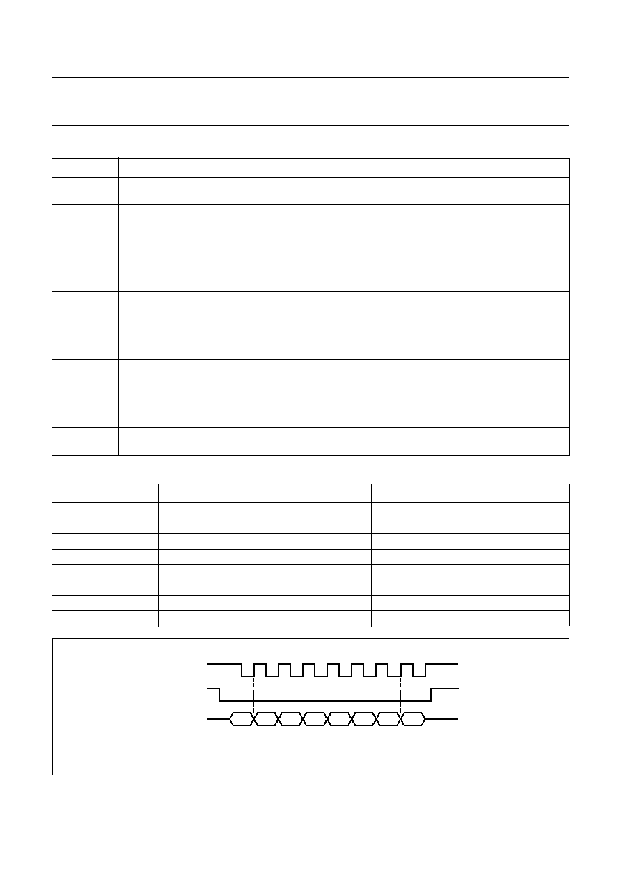
BLOCK DIAGRAM
handbook, full pagewidth
MGB429
SAA7346
I S
OUTPUT
2
SILD
SIDA
MONITOR
CONTROLLER
SICL
WE
OE
CLKIN
CONFIG
FILL
TIMING
RCD2
10
7
CAS
RAS
MICROCONTROLLER
INTERFACE
OTD
SHOCK
DETECTORS
9
SSD
RSB
12
11
35
38
37
36
43
VSS2
VSS1
24
15
17
16
READ
POINTER
WRITE
POINTER
REGISTER
ADDRESS
MULTIPLEXER
I S
INPUT
2
DATA
MULTIPLEXER
42
to
39
V
DD2
V
DD1
1
2
13
19
21 20
22
23 44
WCO
SDO
SCLO
3
4
5
SDI
WCI
SCLI
CFLG
KILL
D0 to D3
S_NSF
KILLOUT
TMS
RESET
8
14
6
18
A0
to
A9
32, 30, 28,
26, 25, 27,
29, 31, 33,
34
Fig.1 Simplified SAA7347 block diagram.

July 1994
4
Philips Semiconductors
Preliminary specification
Shock absorbing RAM addresser
SAA7346
PINNING
SYMBOL
PIN
DESCRIPTION
CFLG
1
correction flag input from CD decoder
KILL
2
kill input
SCLI
3
multi-speed I
2
S bit clock input
WCI
4
multi-speed I
2
S word clock input
SDI
5
multi-speed I
2
S data input
CONFIG
6
external DRAM select input; HIGH 4 Mbit, LOW 1 Mbit
CLKIN
7
16.9344 MHz system clock input
TMS
8
test mode select input; active HIGH
OTD
9
on/off track detector input
RCD2
10
DRAM read cycle divide-by-2 input; active HIGH
SSD
11
shock detected output; active HIGH when shock is detected
RSB
12
rotational shock busy output; active HIGH when rotational shock is detected
S_NSF
13
synthetic new subcode frame output
RESET
14
reset enable input; active LOW
SIDA
15
microcontroller interface input/output data line
SICL
16
microcontroller interface clock input
SILD
17
microcontroller interface read/write input
FILL
18
FIFO write enable output; active HIGH
KILLOUT
19
open drain output; active LOW; when in by-pass mode KILLOUT equals KILL
SDO
20
I
2
S data output
SCLO
21
I
2
S bit clock output
WCO
22
I
2
S word clock output
V
DD1
23
supply voltage 1
V
SS1
24
supply ground 1
A4
25
DRAM address bus output 4
A3
26
DRAM address bus output 3
A5
27
DRAM address bus output 5
A2
28
DRAM address bus output 2
A6
29
DRAM address bus output 6
A1
30
DRAM address bus output 1
A7
31
DRAM address bus output 7
A0
32
DRAM address bus output 0
A8
33
DRAM address bus output 8
A9
34
DRAM address bus output 9
OE
35
DRAM enable output; active LOW
RAS
36
DRAM row address strobe output; active LOW
CAS
37
DRAM column address strobe output; active LOW
WE
38
DRAM write enable output; active LOW
July 1994
5
Philips Semiconductors
Preliminary specification
Shock absorbing RAM addresser
SAA7346
D3 to D0
39 to 42
DRAM data bus inputs/outputs
V
SS2
43
supply ground 2
V
DD2
44
supply voltage 2
SYMBOL
PIN
DESCRIPTION
Fig.2 Pin configuration.
handbook, full pagewidth
MGB430
1
2
3
4
5
6
7
8
9
10
11
33
32
31
30
29
28
27
26
25
24
23
12
13
14
15
16
17
18
19
20
21
22
44
43
42
41
40
39
38
37
36
35
34
A8
A0
A7
A1
A6
A2
A5
A3
A4
CFLG
RCD2
KILL
SCLI
WCI
SDI
CONFIG
CLKIN
TMS
OTD
V
SS1
SAA7346
WCO
S_NSF
RESET
SIDA
SICL
SILD
FILL
KILLOUT
SCLO
SDO
RSB
V
DD2
V
SS2
SSD
V
DD1
A9
D0
D1
D2
D3
WE
CAS
OE
RAS
FUNCTIONAL DESCRIPTION
I
2
S input/output interfaces
The SAA7346 contains an asynchronous serial input and
a serial output interface. The serial operation of the
interfaces is under hardware control of the external
circuitry and uses the I
2
S protocol. The output presents a
continuous clock signal SCLO (typically 2.8224 MHz)
which is divided from the system clock, and a word select
signal WCO, typically 44.1 kHz (f
s
), which is used to
distinguish between right and left channels. When in
by-pass mode WCO and SCLO are the same as the input
interface signals WCI and SCLI, enabling data to pass
through the SAA7346. Since the serial input port is
asynchronous the device is independent of the CD
decoder clock speed and enables the word clock to vary
from 1.1
◊
f
s
to 4
◊
f
s
(typically 2
◊
f
s
). This is a requirement
of any electronic shock absorbing system since the disc
must be rotating faster than usual to assure the FIFO is full
to absorb a shock. The falling edge of WCO indicates the
start of a new transfer. Data is exchanged over the
SDI and SDO pins. The SAA7346 is compatible with a
variety of DAC ICs.
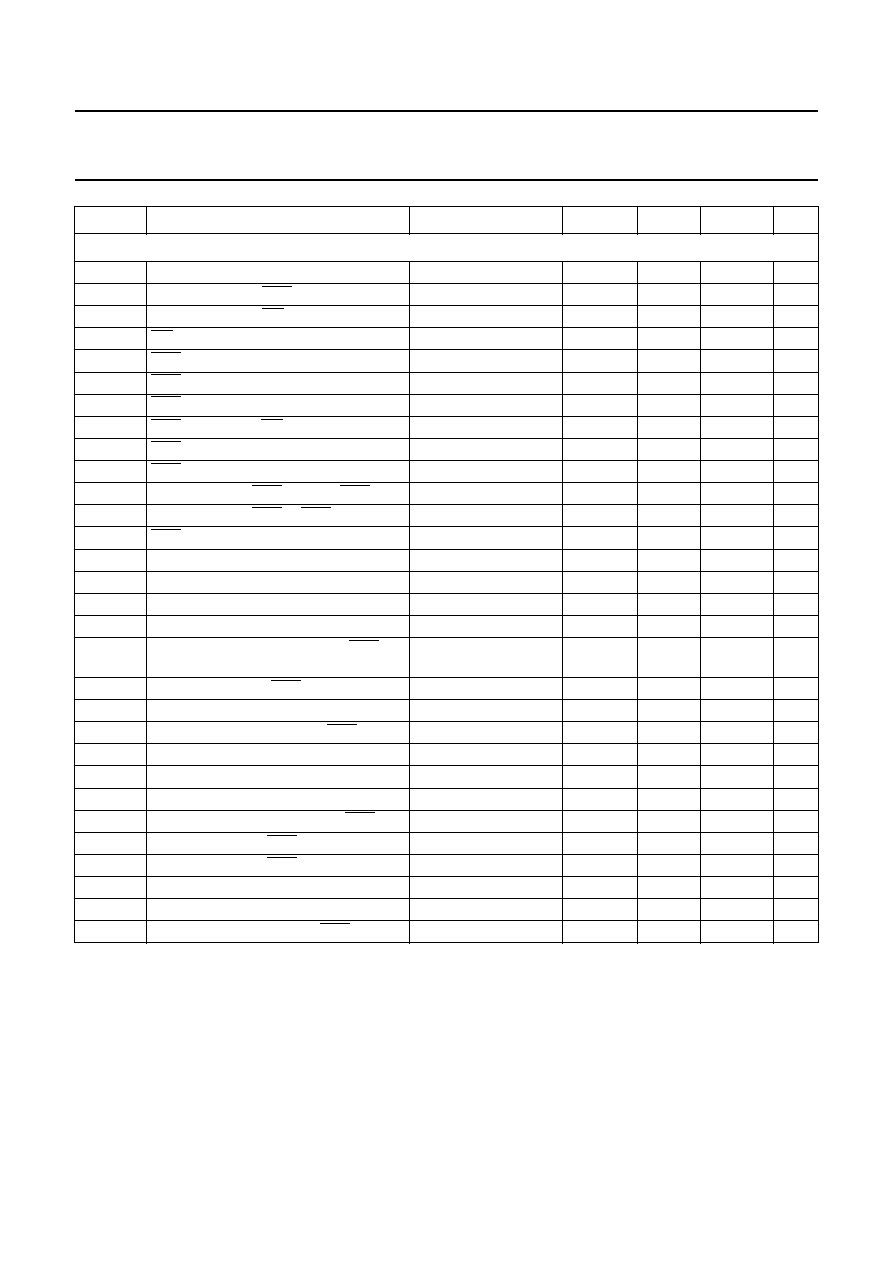
New subcode frame regeneration
The SAA7346 has a digital phase-locked loop (PLL)
system which decodes the F1 and F6 flags, from the first
1-bit signal generated by the CD decoder correction flag
output shown in Fig.3. The F1 flag is the absolute time
sync signal of the New Subcode Frame (NSF). It relates

July 1994
6
Philips Semiconductors
Preliminary specification
Shock absorbing RAM addresser
SAA7346
the position of the subcode-sync to the audio data. This
signal determines the accuracy with which the SAA7346
sews audio data together after a shock. When the CD
decoder preforms a jump the NSF will be missed. The PLL
system will insert the missing pulse. The resulting signal is
the S_NSF which can be used as a time out for reading the
subcode from the decoder shown in Fig.4. The S_NSF is
available externally and the NSF flag can be read via the
serial microcontroller interface. The F6 flag indicates at
least one hold has occurred in the decoder's error
corrector and interpolator. The shock processor uses this
signal to evaluate whether a shock has occurred.
handbook, full pagewidth
F1
F2
F3
F4
F5
F6
F7
F1
11.3
µ
s
45.4
µ
s
MGA370
CFLG
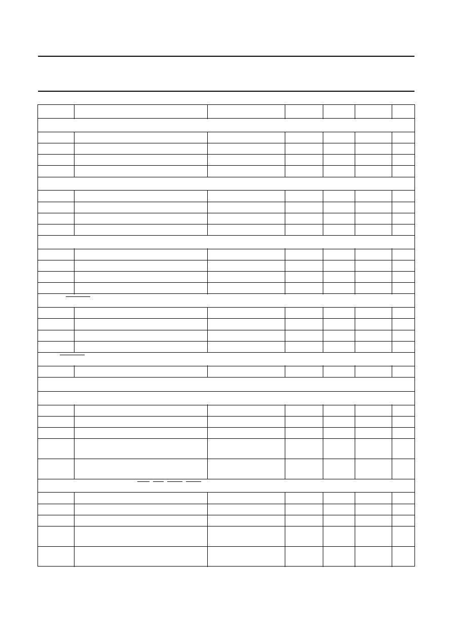
Fig.3 CFLG input timing diagram.
handbook, full pagewidth
Variable
NSF is set until read
by the microcontroller
0.37 ms
6.6 ms
S_NSF
NSF
MGB431
Fig.4 S_NSF output timing diagram; n = 2.
Shock processor
The shock processor determines whether a shock has
occurred by processing all the shock detectors. The
SAA7346 will enter shock mode and set SSD when the:
∑ µ
Csd flag is set by the microcontroller in the command
register
∑
OTD input is active while the jmp_bz flag is not set
∑
RSB output is set while the e_rot_sd flag is set
∑
NSF pulse is lost and the full flag is not read by the
microcontroller from the status register.
When the target position has been found the
microcontroller should set the PFB flag in the command
register. The SAA7346 will respond by clearing the SSD
flag and start refilling. If CFLG still indicates a hold, the
decoder is rolling out of its FIFO. RSB will be set which
sets SSD again thus the FIFO will not start refilling. The
microcontroller should jump one track back and look for
the correct target position again. When the motor speed is
stable and the decoder does not roll out of its FIFO, the
audio data will be glued together.
SSD will be reset whenever the microcontroller sets PFB
or the flush flags in the command register, or when the
FIFO empties while the echo flag is LOW. Note if the
microcontroller wants SSD to be clear for a while the shock
detectors should be inhibited.
FIFO controller and monitor
The SAA7346 uses a state machine to control and monitor
the conditions of the FIFO shown in Fig.5.
July 1994
7
Philips Semiconductors
Preliminary specification
Shock absorbing RAM addresser
SAA7346
Fig.5 State machine flow diagram.
handbook, full pagewidth
SHOCK
7
HOLD
4
first nibble
FILL
3
FILL
1
FILL
2
SSD
NSF +
S_NSF
SSD
SSD
RESET
0
reset and sow
flush + reset
flush + reset +
(empty and echo)
HOLD
5
HOLD
6
first nibble
full
SSD
PFB
PFB
flush + reset
SSD and
(NSF + S_NSF)
MGB432
During normal operation the FIFO will fill up because
writing is carried out twice as fast as reading; this is the fill
mode. If the FIFO is full the monitor will detect and set the
full flag. At the same time the fill flag will be reset thus
preventing audio data from being written in to the FIFO.
When the microcontroller reads the full flag from the status
register, the servo control should jump back one track. The
microcontroller enters a wait loop until the same absolute
time subcode frame turns by again; this is the hold mode.
When the spot is found again the microcontroller should
set the PFB flag in the command register and the
SAA7346 will resume writing to the DRAM. While in fill
mode the write pointer address is saved at the end of each
subcode frame. When the player exists hold mode it
restores the saved address and continues writing after the
last sample.
When a shock is detected the SAA7346 will enter shock
mode. The shock mode will last until the PFB is set by the
microcontroller or the FIFO is flushed, reset or runs empty.
Microcontroller interface
The SAA7346 has a 3-line microcontroller interface which
is compatible with TDA1301, TDA1303 and SAA7345.
W
RITING DATA TO THE
SAA7346
The SAA7346 command register is shown in Table 1. This
can be written to via the microcontroller interface as shown
in Fig.6. The command register flags functions are shown
in Table 2.
Table 1
SAA7346 microcontroller interface registers.
REGISTER
BIT 7
BIT 6
BIT 5
BIT 4
BIT 3
BIT 2
BIT 1
BIT 0
Command
flush
bypass
echo
jmp_bz
otd_p
e_rot_sd
µ
Csd
PFB
Status
Lm
Lm1
FRM_ER
NSF
full
empty
SSD
fill

July 1994
8
Philips Semiconductors
Preliminary specification
Shock absorbing RAM addresser
SAA7346
Table 2
Command register flag functions.
COMMAND
DESCRIPTION
Flush
Flush, when set, will empty the FIFO, reset the read and write pointer addresses. Then writing will
resume to the FIFO. Flag reset automatically.
Bypass
Bypass, when set, will power down the SAA7346. The I
2
S interface passes input to output directly.
The parallel interface port controls RAS, CAS, WE and OE which are pulled HIGH. KILL passes
directly to KILLOUT. When exiting by-pass mode the FIFO is automatically flushed.
Echo
Echo, when set, will cause the FIFO contents to be continuously played until the correct position is
found again.
jmp_bz
Jump busy, when set, indicates a jump is being preformed. The OTD shock detector input will be
disabled. After the jump has finished the flag should be reset by a write.
otd_p
OTD polarity enable. Enables the polarity of the OTD input to be switched from active HIGH set,
active LOW not set.
e_rot_sd
Enable rotational shock detection, when set, will detect shocks whenever the decoder rolls out of its
internal FIFO.
µ
Csd
Microcontroller shock detected is set when the microcontroller has detected a shock.
PFB
Position Found Back, when set, indicates that the microcontroller has found the absolute time frame
after a shock or hold cycle. The audio data will sew together and the flag reset automatically.
Fig.6 Microcontroller WRITE timing.
handbook, full pagewidth
B7
B6
B5
B4
B3
B2
B1
B0
SICL
SILD
SIDA
MGB433
Writing operation sequence:
∑
SILD is held HIGH by the microcontroller.
∑
Microcontroller data is clocked into the internal
command register on the LOW-to-HIGH clock transition
of SICL.
∑
SILD is pulled LOW by the microcontroller to latch-in
data to the command register.
∑
SICL and SILD are pulled HIGH by the microcontroller
to indicate that communications have finished.
R
EADING STATUS OF
SAA7346
The SAA7346 has a status register shown in Table 1. This
can be read via the microcontroller interface shown in
Fig.7. The internal status signals are made available on
the SIDA pin and are shown in Table 3.
July 1994
9
Philips Semiconductors
Preliminary specification
Shock absorbing RAM addresser
SAA7346
Table 3
Internal status signals.
Table 4
FIFO length as a function of CONFIG, Lm and Lm1.
STATUS
DESCRIPTION
Lm and Lm1
The two Most Significant Bits (MSB) of the FIFO. These can be used to display the FIFO length or
correct the subcode time information. The FIFO length is shown in Table 4.
FRM_ER
Framing error flag is set when:
1. The microcontroller did not accept the previous subcode flag on time. When this occurs the NSF
flag will be set together with FRM_ER.
2. The S_NSF generated signal does not coincide with the NSF signal generated by the decoder.
When this occurs there has been a FIFO overflow in the decoder or a jump.
Framing error flag is reset when status register is read.
NSF
New subcode frame is set when an absolute sync is recovered from the CFLG input. Reset when
status register is read. If the NSF is still set at the next occurrence of a subcode frame, FRM_ER will
be set indicating that the microcontroller has lost a frame.
Full
Full is set when the FIFO is full. When the flag is set the microcontroller must jump back to the
previous track. Reset when status register is read.
Empty
Empty is set when the FIFO is emptied during hold or shock modes. DRAM writing should resume
immediately unless echo is set in the command register. If set, writing can only resume when PFB or
flush are set in the command register. The latter will cause a discontinuity in music. Note when set
there is a complete word left in the FIFO giving the SAA7346 controller time to switch to fill mode.
SSD
Set shock detect is set when SAA7346 detects a shock.
Fill
Fill is set when writing data to the DRAM or by setting the command register flags PFB or flush. Reset
internally when full or SSD are set.
CONFIG
Lm
Lm1
FIFO LENGTH (s)
0
0
0
0.00 to 0.19
0
0
1
0.19 to 0.39
0
1
0
0.39 to 0.58
0
1
1
0.58 to 0.78
1
0
0
0.00 to 0.75
1
0
1
0.75 to 1.50
1
1
0
1.50 to 2.25
1
1
1
2.25 to 2.97
Fig.7 Microcontroller READ timing.
handbook, full pagewidth
B7
B6
B5
B4
B3
B2
B1
B0
SICL
SILD
SIDA
MGB434
July 1994
10
Philips Semiconductors
Preliminary specification
Shock absorbing RAM addresser
SAA7346
Read operation sequence:
∑
SILD is held LOW by the microcontroller.
∑
Status information is clocked from the internal status
register on the LOW-to-HIGH clock transition of SICL.
∑
SICL and SILD are pulled HIGH by the microcontroller
to indicate that communications have finished.
DRAM interface
The SAA7346 may be connected to all standard 80 ns,
1M
◊
4 bit or 256K
◊
4 bit fast page mode DRAMs. The
best performance can be expected with the 4 Mbit DRAM.
The CONFIG input selects the DRAM configuration either
HIGH 4 Mbit or LOW 1 Mbit format. The SAA7346
converts audio data from serial to parallel and stores it as
4 bits. The addresses for read or write actions are
calculated by separate read and write pointers which are
multiplexed onto a 4 bits address bus. The control signal
outputs associated with the parallel inputs/outputs are
shown in Table 5.
Table 5
Command register flag functions.
When the SAA7346 leaves bypass mode where all parallel
Port control lines are pulled HIGH, the device initiates a
DRAM power-up routine in accordance with the JEDEC
standard.
COMMAND
DESCRIPTION
WE
indicates write enable action
RAS
row address strobe
CAS
column address strobe
OE
output buffer enable for external memory
during cycle.
System clock
The system clock input, CLKIN, recommended input signal
is 16.9344 MHz. The accuracy of this clock influences the
accuracy of the I
2
S output, therefore the performance of
the DAC and hence audio quality. The system clock is
divided by 384 to derive the I
2
S output word clock, WCO
divided by 8 to derive the I
2
S output bit clock, SCLO.
Therefore whatever clock jitter the user introduces on the
CLKIN signal will be reflected in the WCO and SCLO
outputs.
Reset
Reset should be applied for four system clock cycles.
Reset will:
∑
Clear SSD
∑
Clear the command register but leave the bypass flag
set.
After a reset has been applied the SAA7346 will start-up in
bypass mode.
Kill interface
The kill interface can be used to deactivate the DAC. The
kill input is passed directly to the KILLOUT output when the
bypass flag in the command register is set. When the flag
is not set KILLOUT is generated by the SAA7346. It is
LOW after leaving bypass mode, a reset or a FIFO flush. It
will be LOW until the first error free word is read from the
FIFO. The kill input has no effect or function when the
bypass flag is not set.
Read cycle divide (RCD2)
The RCD2 input enables the modes of operation shown in
Table 6. When RCD2 is HIGH the DRAM-read requests
are halved allowing I
2
S output speeds to vary. The factor
n is called the over-speed factor.
July 1994
11
Philips Semiconductors
Preliminary specification
Shock absorbing RAM addresser
SAA7346
Table 6
SAA7346 I
2
S output speeds.
Notes
1. CAV with n = 4 speed at outer edge of disc; n = 1.5 at inner edge of disc.
2. To build-up a delay, RCD2 should be made HIGH temporarily for twice the delay time.
LIMITING VALUES
In accordance with the Absolute Maximum Rating System (IEC 134).
THERMAL CHARACTERISTICS
CHARACTERISTICS
V
DD
= 3.3 to 5.5 V; V
SS
= 0 V; T
amb
=
-
40 to +85
∞
C; unless otherwise specified.
RCD2
I
2
S INPUT
SPEED
I
2
S OUTPUT
SPEED
APPLICATION
LOW
CAV
(1)
n = 1
CAV CDROM player with standard audio speed
LOW
(2)
n = 1
n = 1
delay line feature
LOW
n = 2
n = 1
shock proof CD player
LOW
n = 4
n = 1
high data rate CDROM/CDI player with standard audio speed
HIGH
n = 2
n =
1
/
2
musicians feature
HIGH
n = 4
n =
1
/
2
musicians feature
SYMBOL
PARAMETER
MIN.
MAX.
UNIT
V
DD
supply voltage
0
6.5
V
P
max
maximum power dissipation
-
500
mW
T
stg
storage temperature
-
55
+125
∞
C
T
amb
operating ambient temperature
-
40
+85
∞
C
SYMBOL
PARAMETER
VALUE
UNIT
R
th j-a
thermal resistance from junction to ambient in free air
80
K/W
SYMBOL
PARAMETER
CONDITIONS
MIN.
TYP.
MAX.
UNIT
Supply
V
DD
supply voltage
3.3
5.0
5.5
V
I
DD
supply current
V
DD
= 5.0 V
-
12
-
mA
I
DDb
bypass supply current
V
DD
= 5.0 V;
bypass mode
-
4
-
mA
I
DDq
quiescent supply current
-
-
100
µ
A
Digital inputs
I
NPUTS
: WCI, SDI, CLKIN, OTD
AND
RCD2;
NORMAL
CMOS
V
IL
LOW level input voltage
-
0.3
-
0.3V
DD
V
V
IH
HIGH level input voltage
0.7V
DD
-
V
DD
+ 0.3 V
I
LI
input leakage current
V
I
= 0 V to V
DD
-
10
-
+10
µ
A
C
I
input capacitance
-
-
10
pF
July 1994
12
Philips Semiconductors
Preliminary specification
Shock absorbing RAM addresser
SAA7346
I
NPUT
CLKIN
f
clk
system clock frequency
-
16.9344
-
MHz
t
H
system clock HIGH time
35
-
65
ns
t
r
system clock rise time
0.8 V to (V
DD
-
0.8 V)
-
-
20
ns
t
f
system clock fall time
(V
DD
-
0.8 V) to 0.8 V
-
-
20
ns
I
NPUTS
: CFLG, KILL, CONFIG
AND
SILD;
WITH PULL
-
UP
V
IL
LOW level input voltage
-
0.3
-
0.3V
DD
V
V
IH
HIGH level input voltage
0.7V
DD
-
V
DD
+ 0.3 V
R
PU
input pull-up resistance
V
I
= 0 V
-
50
-
k
C
I
input capacitance
-
-
10
pF
I
NPUT
TMS;
WITH PULL
-
DOWN
V
IL
LOW level input voltage
-
0.3
-
0.3V
DD
V
V
IH
HIGH level input voltage
0.7V
DD
-
V
DD
+ 0.3 V
R
PD
input pull-down resistance
V
I
= V
DD
-
50
-
k
C
I
input capacitance
-
-
10
pF
I
NPUTS
: RESET, SCLI
AND
SICL; S
CHMITT
-
TRIGGER
V
thr
switching threshold voltage rising
-
-
0.8V
DD
V
V
thf
switching threshold voltage falling
0.2V
DD
-
-
V
V
hys
hysteresis voltage
-
0.33V
DD
-
V
C
I
input capacitance
-
-
10
pF
I
NPUT
RESET
t
RW
RESET pulse width; active LOW
236
-
-
ns
Digital outputs
O
UTPUTS
: FILL, S_NSF, RSB
AND
SSD;
PUSH
-
PULL
V
OL
LOW level output voltage
I
OL
= 4 mA
0
-
0.4
V
V
OH
HIGH level output voltage
I
OL
=
-
4 mA
V
DD
-
0.4
-
V
DD
V
C
L
load capacitance
-
-
50
pF
t
r
output rise time
0.8 V to (V
DD
-
0.8 V);
C
L
= 50 pF
-
-
15
ns
t
f
output fall time
(V
DD
-
0.8 V) to 0.8 V;
C
L
= 50 pF
-
-
15
ns
O
UTPUTS
: SDO, SCLO, WCO, WE, OE, RAS, CAS, A0
TO
A9;
SLEW RATE PUSH
-
PULL
V
OL
LOW level output voltage
I
OL
= 4 mA
0
-
0.4
V
V
OH
HIGH level output voltage
I
OL
=
-
4 mA
V
DD
-
0.4
-
V
DD
V
C
L
load capacitance
-
-
50
pF
t
r
output rise time
0.8 V to (V
DD
-
0.8 V);
C
L
= 50 pF
-
-
20
ns
t
f
output fall time
(V
DD
-
0.8 V) to 0.8 V;
C
L
= 50 pF
-
-
20
ns
SYMBOL
PARAMETER
CONDITIONS
MIN.
TYP.
MAX.
UNIT
July 1994
13
Philips Semiconductors
Preliminary specification
Shock absorbing RAM addresser
SAA7346
O
UTPUT
KILLOUT;
OPEN DRAIN
V
OL
LOW level output voltage
I
OL
= 2 mA
0
-
0.4
V
I
O
output current
-
-
2
mA
C
L
load capacitance
-
-
50
pF
t
f
output fall time
(V
DD
-
0.8 V) to 0.8 V;
C
L
= 50 pF
-
-
30
ns
I
NPUTS
/
OUTPUTS
: D0
TO
D3;
NORMAL
CMOS
WITH SLEW RATE CONTROLLED PUSH
-
PULL
V
IL
LOW level input voltage
-
0.3
-
0.3V
DD
V
V
IH
HIGH level input voltage
0.7V
DD
-
V
DD
+ 0.3 V
I
LI
input leakage current
V
I
= 0 V to V
DD
-
10
-
+10
µ
A
C
I
input capacitance
-
-
10
pF
V
OL
LOW level output voltage
I
OL
= 4 mA
0
-
0.4
V
V
OH
HIGH level output voltage
I
OL
=
-
4 mA
V
DD
-
0.4
-
V
DD
V
C
L
load capacitance
-
-
50
pF
t
r
output rise time
0.8 V to (V
DD
-
0.8 V);
C
L
= 50 pF
-
-
20
ns
t
f
output fall time
(V
DD
-
0.8 V) to 0.8 V;
C
L
= 50 pF
-
-
20
ns
I
NPUT
/
OUTPUT
SIDA;
NORMAL
CMOS
WITH PUSH
-
PULL
V
IL
LOW level input voltage
-
0.3
-
0.3V
DD
V
V
IH
HIGH level input voltage
0.7V
DD
-
V
DD
+ 0.3 V
I
LI
input leakage current
V
I
= 0 V to V
DD
-
10
-
+10
µ
A
C
I
input capacitance
-
-
10
pF
V
OL
LOW level output voltage
I
OL
= 4 mA
0
-
0.4
V
V
OH
HIGH level output voltage
I
OL
=
-
4 mA
V
DD
-
0.4
-
V
DD
V
C
L
load capacitance
-
-
50
pF
t
r
output rise time
0.8 V to (V
DD
-
0.8 V);
C
L
= 50 pF
-
-
15
ns
t
f
output fall time
(V
DD
-
0.8 V) to 0.8 V;
C
L
= 50 pF
-
-
15
ns
I
2
S timing
R
ECEIVER
(
SEE
F
IG
.9)
Clock input SCLI
T
cy
clock cycle time
118.1
(1)
236.2
(2)
472.4
(3)
ns
t
H
clock HIGH time
41.3
(1)
-
-
ns
t
L
clock LOW time
41.3
(1)
-
-
ns
Inputs: SDI and WCI
t
su
set-up time
23.6
-
-
ns
t
h
hold time
10
-
-
ns
SYMBOL
PARAMETER
CONDITIONS
MIN.
TYP.
MAX.
UNIT
July 1994
14
Philips Semiconductors
Preliminary specification
Shock absorbing RAM addresser
SAA7346
T
RANSMITTER
(
SEE
F
IG
.8)
Clock output SCLO
T
cy
clock cycle time
-
472.4
(3)
944.8
(4)
ns
t
H
clock HIGH time
165.3
-
-
ns
t
L
clock LOW time
165.3
-
-
ns
Outputs: SDO and WCO
t
d
delay time
-
-
377
ns
t
h
hold time
40
-
-
ns
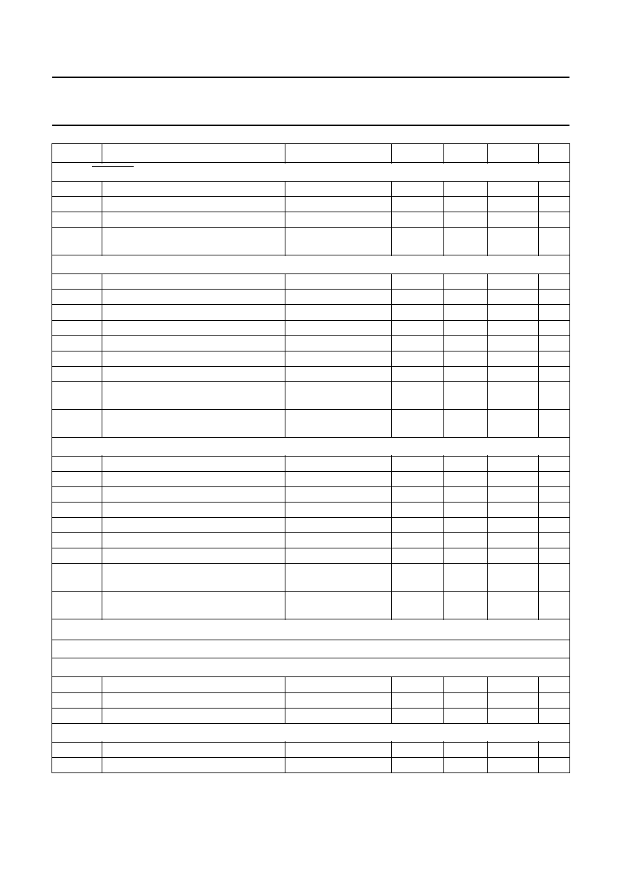
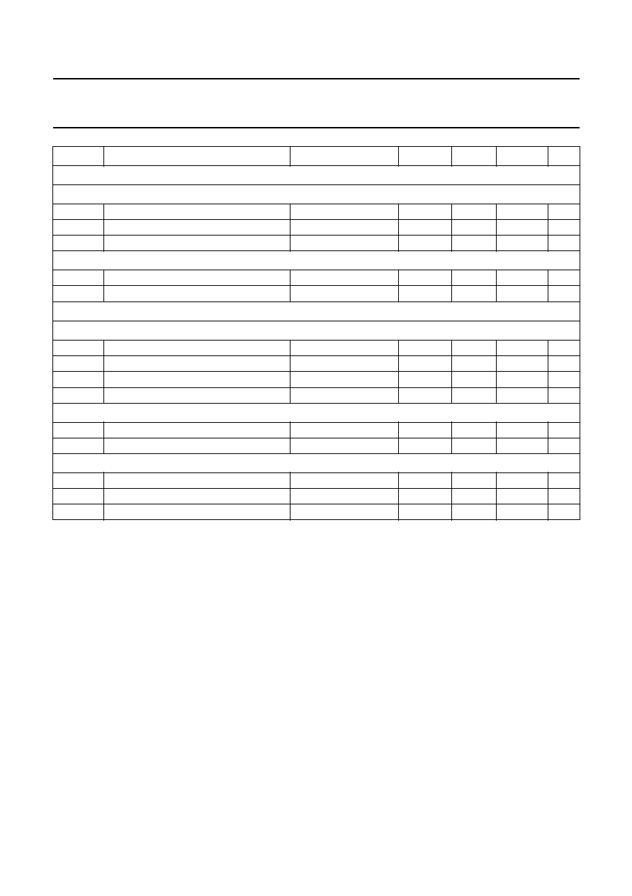
Microcontroller interface timing (see Figs 12 and 13)
I
NPUTS
: SICL
AND
SILD
t
H
input HIGH time
180
-
-
ns
t
L
input LOW time
180
-
-
ns
t
r
rise time
0.8 V to (V
DD
-
0.8 V)
-
-
240
ns
t
f
fall time
(V
DD
-
0.8 V) to 0.8 V
-
-
240
ns
Read mode (see Fig.12)
t
d
delay time SILD to SIDA valid
120
-
-
ns
t
pd
propagation delay time SICL to SIDA
-
-
110
ns
Write mode (see Fig.13)
t
su1
set-up time SIDA to SICL
40
-
-
ns
t
h
hold time SICL to SIDA
-
-
180
ns
t
su2
set-up time SICL to SILD
180
-
-
ns
SYMBOL
PARAMETER
CONDITIONS
MIN.
TYP.
MAX.
UNIT
July 1994
15
Philips Semiconductors
Preliminary specification
Shock absorbing RAM addresser
SAA7346
Notes
1. n = 4.
2. n = 2.
3. n = 1.
4. n =
1
/
2
.
DRAM interface timing (see Figs 14 and 15)
T
cy
read or write cycle time
160
-
-
ns
t
CAC
access time from CAS
-
-
20
ns
t
OAC
access time from OE
-
-
20
ns
t
h3
OE to data input hold time
0
-
-
ns
t
RH
RAS HIGH time
70
-
-
ns
t
RL
RAS LOW time
80
-
10000
ns
t
h1
RAS hold time
20
-
-
ns
t
h2
RAS hold time to OE LOW
20
-
-
ns
t
CL
CAS LOW time
20
-
10000
ns
t
h4
CAS hold time
80
-
-
ns
t
CRd
delay time from CAS HIGH to RAS
10
-
-
ns
t
RCd
delay time from RAS to CAS
25
-
-
ns
t
Rd
RAS to column address delay time
20
-
-
ns
t
su1
row address set-up time
0
-
-
ns
t
RAh
row address hold time
15
-
-
ns
t
su2
column address set-up time
0
-
-
ns
t
CAh
column address hold time
20
-
-
ns
t
Rh
column address hold time from RAS
LOW
60
-
-
ns
t
l
column address to RAS lead time
40
-
-
ns
t
RCh
read command hold time
0
-
-
ns
t
RRh
read command hold time to RAS
12
-
-
ns
t
Wsu
write command set-up time
0
-
-
ns
t
Wh1
write command hold time
15
-
-
ns
t
WL
write command LOW time
15
-
-
ns
t
Wh2
write command hold time from RAS
60
-
-
ns
t
WCl
write command to CAS lead time
20
-
-
ns
t
WRl
write command to RAS lead time
20
-
-
ns
t
Dsu
data output set-up time
0
-
-
ns
t
Dh
data output hold time
15
-
-
ns
t
DRh
data output hold time from RAS
60
-
-
ns
SYMBOL
PARAMETER
CONDITIONS
MIN.
TYP.
MAX.
UNIT
July 1994
16
Philips Semiconductors
Preliminary specification
Shock absorbing RAM addresser
SAA7346
Fig.8 I
2
S input timing.
handbook, full pagewidth
DD
V ≠ 0.8 V
0.8 V
DD
V ≠ 0.8 V
0.8 V
t H
MGB436
t L
SCLI
SDI
WCI
t h
t su
Tcy
Fig.9 I
2
S output timing.
handbook, full pagewidth
DD
V ≠ 0.8 V
0.8 V
DD
V ≠ 0.8 V
0.8 V
t H
MGB435
t L
Tcy
SCLO
SDO
WCO
t h
t d
handbook, full pagewidth
LEFT CHANNEL
RIGHT CHANNEL
µ
5.67 s
SCLI
WCI
SDI
MSB
LSB
LSB
MSB
4.2336 MHz
88.2 kHz
MGB437
Fig.10 Typical I
2
S data input waveform; f = 4.2 MHz; n = 2.

July 1994
17
Philips Semiconductors
Preliminary specification
Shock absorbing RAM addresser
SAA7346
handbook, full pagewidth
LEFT CHANNEL
RIGHT CHANNEL
µ
11.34 s
SCLO
WCO
SDO
MSB
LSB
LSB
MSB
2.1168 MHz
44.1 kHz
MGB438
Fig.11 Typical I
2
S data output waveform; f = 2.1 MHz; n = 1.
Fig.12 Microcontroller timing; READ mode.
handbook, full pagewidth
DD
V ≠ 0.8 V
0.8 V
DD
V ≠ 0.8 V
0.8 V
tH
MGB439
t L
t r
SILD
SICL
SIDA
DD
V ≠ 0.8 V
0.8 V
t f
td
f
t
t r
t pd
July 1994
18
Philips Semiconductors
Preliminary specification
Shock absorbing RAM addresser
SAA7346
Fig.13 Microcontroller timing; WRITE mode.
handbook, full pagewidth
DD
V ≠ 0.8 V
0.8 V
DD
V ≠ 0.8 V
0.8 V
tH
MGB440
t L
t r
DD
V ≠ 0.8 V
0.8 V
t f
t su2
SILD
SICL
SIDA
t su1
t L
t f
t r
t h
July 1994
19
Philips Semiconductors
Preliminary specification
Shock absorbing RAM addresser
SAA7346
This text is here in white to force landscape pages to be rotated correctly when browsing through the pdf in the Acrobat reader.This text is here in
_
white to force landscape pages to be rotated correctly when browsing through the pdf in the Acrobat reader.This text is here inThis text is here in
white to force landscape pages to be rotated correctly when browsing through the pdf in the Acrobat reader. white to force landscape pages to be ...
handbook, full pagewidth
RAS
CAS
A0
to
A9
tRH
V ≠ 0.8V
DD
0.8 V
tRL
tRh
t CRd
t h4
t CL
t h1
t RCd
t CRd
V ≠ 0.8V
DD
0.8 V
t su1
t RAh
COLUMN
ROW
t su2
t CAh
t l
t Rd
V ≠ 0.8V
DD
0.8 V
WE
OE
t RCh
t RRh
V ≠ 0.8V
DD
0.8 V
t CAC
t OAC
t h2
t h3
D0 to D3
INPUT
V ≠ 0.8V
DD
0.8 V
MGB441
Tcy
Fig.14 READ cycle timing.
July 1994
20
Philips Semiconductors
Preliminary specification
Shock absorbing RAM addresser
SAA7346
handbook, full pagewidth
RAS
CAS
A0
to
A9
tRH
V ≠ 0.8V
DD
0.8 V
tRL
tRh
t CRd
t h4
t CL
t h1
t RCd
t CRd
V ≠ 0.8V
DD
0.8 V
t su1
t RAh
COLUMN
ROW
t su2
t CAh
t Rl
t Rd
V ≠ 0.8V
DD
0.8 V
t Wh1
t WL
t Wsu
t Wh2
t RWI
t WCI
V ≠ 0.8V
DD
0.8 V
V ≠ 0.8V
DD
Dh
D0 to D3
OUTPUT
V ≠ 0.8V
DD
0.8 V
MGB442
t
DRh
t
tDsu
WE
OE
Tcy
Fig.15 WRITE cycle timing.
July 1994
21
Philips Semiconductors
Preliminary specification
Shock absorbing RAM addresser
SAA7346
APPLICATION INFORMATION
Fig.16 SAA7346 application diagram.
handbook, full pagewidth
SAA7346
1
2
3
4
5
6
7
8
9
10
11
25 to 34
24
23
22
21
20
19
18
17
16
15
14
13
12
44
43
38
37
36
35
39
to
42
D3 to D0 WE CAS RAS OE
A9 to A0
10
k
VDD
100 nF
I S bus
to DAC
2
5 V
micro-
controller
interface
RESET
RSB
S_NSF
KILLOUT
VDD
100 nF
I S bus from
CD decoder
2
5 V
16.9 MHz
CLKIN
CFLG
KILL
OTD
RCD2
SSD
1 M x 4 bit
DRAM
MGB443

July 1994
22
Philips Semiconductors
Preliminary specification
Shock absorbing RAM addresser
SAA7346
PACKAGE OUTLINE
handbook, full pagewidth
X
A
B
10.1
9.9
12.9
12.3
0.15
M
B
0.40
0.20
pin 1 index
1
44
34
33
23
22
11
0.40
0.20
0.15 M A
0.8
12
0.8
10.1
9.9
12.9
12.3
S
0.1 S
seating
plane
1.2
0.8
(4x)
1.2
0.8
(4x)
0.95
0.55
MBB944 - 2
detail X
0.85
0.75
0.25
0.14
2.10
1.70
0 to 10
o
1.85
1.65
0.25
0.05
Fig.17 Plastic quad flat package; 44 leads (lead length 1.3 mm); body 10
◊
10
◊
1.75 mm; (SOT307-2; QFP44).
Dimensions in mm.

July 1994
23
Philips Semiconductors
Preliminary specification
Shock absorbing RAM addresser
SAA7346
SOLDERING
Plastic quad flat-packs
B
Y WAVE
During placement and before soldering, the component
must be fixed with a droplet of adhesive. After curing the
adhesive, the component can be soldered. The adhesive
can be applied by screen printing, pin transfer or syringe
dispensing.
Maximum permissible solder temperature is 260
∞
C, and
maximum duration of package immersion in solder bath is
10 s, if allowed to cool to less than 150
∞
C within 6 s.
Typical dwell time is 4 s at 250
∞
C.
A modified wave soldering technique is recommended
using two solder waves (dual-wave), in which a turbulent
wave with high upward pressure is followed by a smooth
laminar wave. Using a mildly-activated flux eliminates the
need for removal of corrosive residues in most
applications.
B
Y SOLDER PASTE REFLOW
Reflow soldering requires the solder paste (a suspension
of fine solder particles, flux and binding agent) to be
applied to the substrate by screen printing, stencilling or
pressure-syringe dispensing before device placement.
Several techniques exist for reflowing; for example,
thermal conduction by heated belt, infrared, and
vapour-phase reflow. Dwell times vary between 50 and
300 s according to method. Typical reflow temperatures
range from 215 to 250
∞
C.
Preheating is necessary to dry the paste and evaporate
the binding agent. Preheating duration: 45 min at 45
∞
C.
R
EPAIRING SOLDERED JOINTS
(
BY HAND
-
HELD SOLDERING
IRON OR PULSE
-
HEATED SOLDER TOOL
)
Fix the component by first soldering two, diagonally
opposite, end pins. Apply the heating tool to the flat part of
the pin only. Contact time must be limited to 10 s at up to
300
∞
C. When using proper tools, all other pins can be
soldered in one operation within 2 to 5 s at between 270
and 320
∞
C. (Pulse-heated soldering is not recommended
for SO packages.)
For pulse-heated solder tool (resistance) soldering of VSO
packages, solder is applied to the substrate by dipping or
by an extra thick tin/lead plating before package
placement.
DEFINITIONS
LIFE SUPPORT APPLICATIONS
These products are not designed for use in life support appliances, devices, or systems where malfunction of these
products can reasonably be expected to result in personal injury. Philips customers using or selling these products for
use in such applications do so at their own risk and agree to fully indemnify Philips for any damages resulting from such
improper use or sale.
Data sheet status
Objective specification
This data sheet contains target or goal specifications for product development.
Preliminary specification
This data sheet contains preliminary data; supplementary data may be published later.
Product specification
This data sheet contains final product specifications.
Limiting values
Limiting values given are in accordance with the Absolute Maximum Rating System (IEC 134). Stress above one or
more of the limiting values may cause permanent damage to the device. These are stress ratings only and operation
of the device at these or at any other conditions above those given in the Characteristics sections of the specification
is not implied. Exposure to limiting values for extended periods may affect device reliability.
Application information
Where application information is given, it is advisory and does not form part of the specification.

Philips Semiconductors
Philips Semiconductors ≠ a worldwide company
Argentina: IEROD, Av. Juramento 1992 - 14.b, (1428)
BUENOS AIRES, Tel. (541)786 7633, Fax. (541)786 9367
Australia: 34 Waterloo Road, NORTH RYDE, NSW 2113,
Tel. (02)805 4455, Fax. (02)805 4466
Austria: Triester Str. 64, A-1101 WIEN, P.O. Box 213,
Tel. (01)60 101-1236, Fax. (01)60 101-1211
Belgium: Postbus 90050, 5600 PB EINDHOVEN, The Netherlands,
Tel. (31)40 783 749, Fax. (31)40 788 399
Brazil: Rua do Rocio 220 - 5
th
floor, Suite 51,
CEP: 04552-903-S√O PAULO-SP, Brazil.
P.O. Box 7383 (01064-970).
Tel. (011)821-2327, Fax. (011)829-1849
Canada: INTEGRATED CIRCUITS:
Tel. (800)234-7381, Fax. (708)296-8556
DISCRETE SEMICONDUCTORS: 601 Milner Ave,
SCARBOROUGH, ONTARIO, M1B 1M8,
Tel. (0416)292 5161 ext. 2336, Fax. (0416)292 4477
Chile: Av. Santa Maria 0760, SANTIAGO,
Tel. (02)773 816, Fax. (02)777 6730
Colombia: IPRELENSO LTDA, Carrera 21 No. 56-17,
77621 BOGOTA, Tel. (571)249 7624/(571)217 4609,
Fax. (571)217 4549
Denmark: Prags Boulevard 80, PB 1919, DK-2300 COPENHAGEN S,
Tel. (032)88 2636, Fax. (031)57 1949
Finland: Sinikalliontie 3, FIN-02630 ESPOO,
Tel. (9)0-50261, Fax. (9)0-520971
France: 4 Rue du Port-aux-Vins, BP317,
92156 SURESNES Cedex,
Tel. (01)4099 6161, Fax. (01)4099 6427
Germany: PHILIPS COMPONENTS UB der Philips G.m.b.H.,
P.O. Box 10 63 23, 20043 HAMBURG,
Tel. (040)3296-0, Fax. (040)3296 213.
Greece: No. 15, 25th March Street, GR 17778 TAVROS,
Tel. (01)4894 339/4894 911, Fax. (01)4814 240
Hong Kong: PHILIPS HONG KONG Ltd., Components Div.,
6/F Philips Ind. Bldg., 24-28 Kung Yip St., KWAI CHUNG, N.T.,
Tel. (852)424 5121, Fax. (852)428 6729
India: Philips INDIA Ltd, Components Dept,
Shivsagar Estate, A Block ,
Dr. Annie Besant Rd. Worli, Bombay 400 018
Tel. (022)4938 541, Fax. (022)4938 722
Indonesia: Philips House, Jalan H.R. Rasuna Said Kav. 3-4,
P.O. Box 4252, JAKARTA 12950,
Tel. (021)5201 122, Fax. (021)5205 189
Ireland: Newstead, Clonskeagh, DUBLIN 14,
Tel. (01)640 000, Fax. (01)640 200
Italy: PHILIPS COMPONENTS S.r.l.,
Viale F. Testi, 327, 20162 MILANO,
Tel. (02)6752.3302, Fax. (02)6752 3300.
Japan: Philips Bldg 13-37, Kohnan 2 -chome, Minato-ku, TOKYO 108,
Tel. (03)3740 5028, Fax. (03)3740 0580
Korea: (Republic of) Philips House, 260-199 Itaewon-dong,
Yongsan-ku, SEOUL, Tel. (02)794-5011, Fax. (02)798-8022
Malaysia: No. 76 Jalan Universiti, 46200 PETALING JAYA,
SELANGOR, Tel. (03)750 5214, Fax. (03)757 4880
Mexico: Philips Components, 5900 Gateway East, Suite 200,
EL PASO, TX 79905, Tel. 9-5(800)234-7381, Fax. (708)296-8556
Netherlands: Postbus 90050, 5600 PB EINDHOVEN, Bldg. VB
Tel. (040)783749, Fax. (040)788399
New Zealand: 2 Wagener Place, C.P.O. Box 1041, AUCKLAND,
Tel. (09)849-4160, Fax. (09)849-7811
Norway: Box 1, Manglerud 0612, OSLO,
Tel. (022)74 8000, Fax. (022)74 8341
Pakistan: Philips Electrical Industries of Pakistan Ltd.,
Exchange Bldg. ST-2/A, Block 9, KDA Scheme 5, Clifton,
KARACHI 75600, Tel. (021)587 4641-49,
Fax. (021)577035/5874546.
Philippines: PHILIPS SEMICONDUCTORS PHILIPPINES Inc,
106 Valero St. Salcedo Village, P.O. Box 2108 MCC, MAKATI,
Metro MANILA, Tel. (02)810 0161, Fax. (02)817 3474
Portugal: PHILIPS PORTUGUESA, S.A.,
Rua dr. AntÛnio Loureiro Borges 5, Arquiparque - Miraflores,
Apartado 300, 2795 LINDA-A-VELHA,
Tel. (01)14163160/4163333, Fax. (01)14163174/4163366.
Singapore: Lorong 1, Toa Payoh, SINGAPORE 1231,
Tel. (65)350 2000, Fax. (65)251 6500
South Africa: S.A. PHILIPS Pty Ltd., Components Division,
195-215 Main Road Martindale, 2092 JOHANNESBURG,
P.O. Box 7430 Johannesburg 2000,
Tel. (011)470-5911, Fax. (011)470-5494.
Spain: Balmes 22, 08007 BARCELONA,
Tel. (03)301 6312, Fax. (03)301 42 43
Sweden: Kottbygatan 7, Akalla. S-164 85 STOCKHOLM,
Tel. (0)8-632 2000, Fax. (0)8-632 2745
Switzerland: Allmendstrasse 140, CH-8027 ZÐRICH,
Tel. (01)488 2211, Fax. (01)481 77 30
Taiwan: PHILIPS TAIWAN Ltd., 23-30F, 66, Chung Hsiao West
Road, Sec. 1. Taipeh, Taiwan ROC, P.O. Box 22978,
TAIPEI 100, Tel. (02)388 7666, Fax. (02)382 4382.
Thailand: PHILIPS ELECTRONICS (THAILAND) Ltd.,
209/2 Sanpavuth-Bangna Road Prakanong,
Bangkok 10260, THAILAND,
Tel. (662)398-0141, Fax. (662)398-3319.
Turkey: Talatpasa Cad. No. 5, 80640 GÐLTEPE/ISTANBUL,
Tel. (0 212)279 2770, Fax. (0212)269 3094
United Kingdom: Philips Semiconductors Limited, P.O. Box 65,
Philips House, Torrington Place, LONDON, WC1E 7HD,
Tel. (071)436 41 44, Fax. (071)323 03 42
United States: INTEGRATED CIRCUITS:
811 East Arques Avenue, SUNNYVALE, CA 94088-3409,
Tel. (800)234-7381, Fax. (708)296-8556
DISCRETE SEMICONDUCTORS: 2001 West Blue Heron Blvd.,
P.O. Box 10330, RIVIERA BEACH, FLORIDA 33404,
Tel. (800)447-3762 and (407)881-3200, Fax. (407)881-3300
Uruguay: Coronel Mora 433, MONTEVIDEO,
Tel. (02)70-4044, Fax. (02)92 0601
For all other countries apply to: Philips Semiconductors,
International Marketing and Sales, Building BAF-1,
P.O. Box 218, 5600 MD, EINDHOVEN, The Netherlands,
Telex 35000 phtcnl, Fax. +31-40-724825
SCD31
© Philips Electronics N.V. 1994
All rights are reserved. Reproduction in whole or in part is prohibited without the
prior written consent of the copyright owner.
The information presented in this document does not form part of any quotation
or contract, is believed to be accurate and reliable and may be changed without
notice. No liability will be accepted by the publisher for any consequence of its
use. Publication thereof does not convey nor imply any license under patent- or
other industrial or intellectual property rights.
Printed in The Netherlands
513061/1500/01/pp24
Date of release: July 1994
Document order number:
9397 736 30011