2000 Mar 21
2
Philips Semiconductors
Preliminary specification
Channel encoder/decoder CDR60
SAA7392
CONTENTS
1
FEATURES
2
GENERAL DESCRIPTION
3
QUICK REFERENCE DATA
4
ORDERING INFORMATION
5
BLOCK DIAGRAM
6
PINNING INFORMATION
6.1
Pinning
6.2
Pin description
7
FUNCTIONAL DESCRIPTION
7.1
Microprocessor interfaces
7.2
Register map
7.3
System clocks
7.4
HF analog front-end
7.5
Bit recovery
7.6
Decoder function
7.7
Subcode interface
7.8
Digital output
7.9
Serial output interface
7.10
Motor control
7.11
The serial in function
7.12
The subcode insert function
7.13
The data encoder block
7.14
Encode control block
7.15
The EFM modulator
7.16
The EFM clock generator
7.17
The Wobble processor
8
LIMITING VALUES
9
OPERATING CHARACTERISTICS
9.1
ADC and AGC parameters
10
APPLICATION INFORMATION
10.1
Write start control of encoder in CD-ROM mode
10.2
Write start control of encoder in Audio mode
10.3
Start-up of encode in flow-control operation
10.4
Start-up of encoder in synchronous stream
mode
10.5
Operating CDR60 in CAV mode, flow control
on input stream
10.6
Operating in CLV Mode, Flow Control on Input
Stream
10.7
Operating in CLV Mode, Synchronous Stream
Operation
11
PACKAGE OUTLINE
12
SOLDERING
12.1
Introduction to soldering surface mount
packages
12.2
Reflow soldering
12.3
Wave soldering
12.4
Manual soldering
12.5
Suitability of surface mount IC packages for
wave and reflow soldering methods
13
DEFINITIONS
14
LIFE SUPPORT APPLICATIONS
15
PURCHASE OF PHILIPS I
2
C COMPONENTS
2000 Mar 21
3
Philips Semiconductors
Preliminary specification
Channel encoder/decoder CDR60
SAA7392
1
FEATURES
�
Very high speed Compact Disc (CD) compatible
decoding and encoding device
�
On-chip Analog-to-Digital Converter (ADC) and
Automatic Gain Control (AGC) for HF data capture
�
Eight-to-Fourteen Modulation (EFM)
�
Advanced motor control loop to allow CAV, CLV and
pseudo-CLV playback
�
Integrated FIFO for de-coupling of mechanism speed
and application speed
�
Versatile output interface allowing different I
2
S-bus and
Electronic Industries Association of Japan (EIAJ)
formats
�
Device is fully compatible with ELM, PLUM and Sanyo
CD-ROM block decoders
�
Quad-pass CIRC correction for CD mode
(C1-C2-C1-C2)
�
Subcode/header processing for CD format
�
Frequency multiplier allows use of a 8 MHz crystal.
2
GENERAL DESCRIPTION
CDR60 is a channel encoder/decoder for
CD/CD-R/CD-RW/CD Audio Recorder systems. It
incorporates all logic and RAM required for the complete
encoding and decoding processes.
There are two main datapaths through the CDR60 device.
The decode datapath captures the incoming EFM data
stream via the HF ADC and AGC functions.
The bit detector recovers the individual bits from the
incoming signal, correcting asymmetry, performing noise
filtering and equalisation, and recovering the channel bit
clock using a digital PLL. The demodulator converts the
EFM bits to byte-wide data symbols, before passing them
onto the decoder for subcode extraction, de-interleaving
and error correction. The decoded data is then made
available via the multi-function serial output interface.
The encode datapath takes data symbols from the block
encoder/decoder via the serial data and subcode input
functions, encoding them via the encoder block. The
encoded data stream is passed to the EFM modulator,
which generates the required EFM signal, output as a
digital bit stream. The encode process is controlled via the
Wobble processor, encode control and EFM clock
generator functions.
As well as these two data processing sections, three
further blocks support overall device operation. The
system clock generator provides all digital clocks required
by the CDR60. The motor servo allows the CDR60 to
control the spindle motor and is controlled by the
microprocessor interface. This interface can be accessed
either via a parallel (80C51) or a serial (I
2
C-bus) interface.
3
QUICK REFERENCE DATA
4
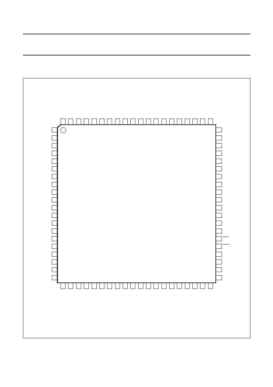
ORDERING INFORMATION
SYMBOL
PARAMETER
MIN.
TYP.
MAX.
UNIT
V
DDD
supply voltage (core and pad ring)
3.0
3.3
3.6
V
V
DDA
supply voltage (analog)
3.0
3.3
3.6
V
V
DDE
supply voltage (output drivers)
3.0
3.3
3.6
V
I
DD
supply current
-
200
-
mA
f
xtal
crystal frequency
8
8.4672
33
MHz
T
amb
operating ambient temperature
0
-
70
�
C
T
stg
storage temperature
-
55
-
+125
�
C
TYPE
NUMBER
PACKAGE
NAME
DESCRIPTION
VERSION
SAA7392HL
LQFP80
plastic low profile quad flat package; 80 leads; body 12
�
12
�
1.4 mm
SOT315-1
2000
Mar
21
4
Philips Semiconductors
Preliminar
y specification
Channel encoder/decoder CDR60
SAA7392
This text is here in white to force landscape pages to be rotated correctly when browsing through the pdf in the Acrobat reader.This text is here in
_
white to force landscape pages to be rotated correctly when browsing through the pdf in the Acrobat reader.This text is here inThis text is here in
white to force landscape pages to be rotated correctly when browsing through the pdf in the Acrobat reader. white to force landscape pages to be ...
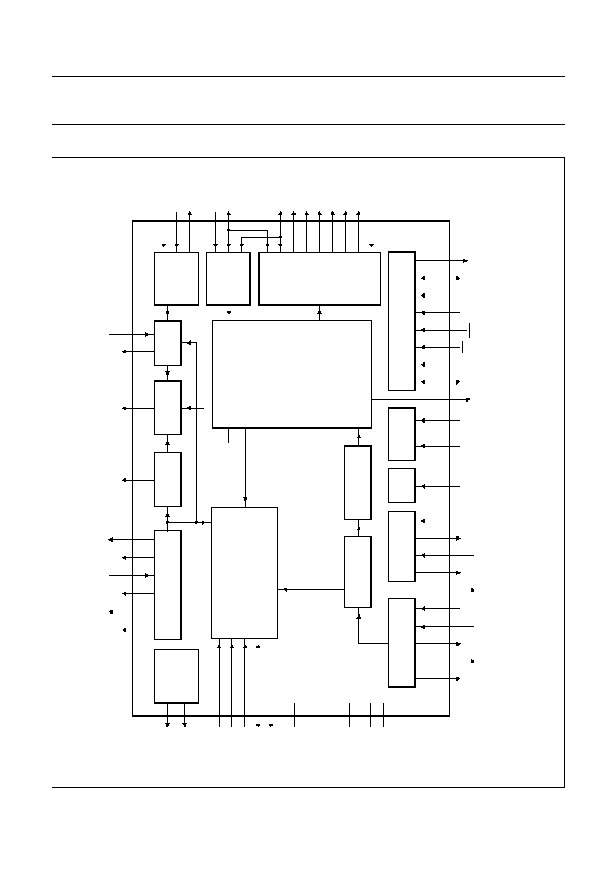
5
BLOCK DIA
GRAM
d
book, full pagewidth
SAA7392
MGR791
SUB-CPU INTERFACE
SERIAL OUT
51
PCAin
58
FLAG
54
STOPCK
59
DATAO
56
EBUOUT
55
V4
57
SYNC
61
BCLK
SERIAL IN
SUBCODE
INSERT
60
WCLK
64
DATAI
66
RCK
67
SFSY
65
SUB
34
INT
33
SDA
32
SCL
50
CSi
45
WRi
46
RDi
47
ALE
68
CFLG
35
to
42
DA7
to
DA0
ENCODE
CONTROL
27
PANIC
77
LASERON
EFM
MODULATOR
79
EFMDATA
IREF
GENERATOR
EFM CLOCK
GENERATOR
78
XEFM
WOBBLE
PROCESSOR
MOTOR/TACHO
INTERFACE
ERROR CORRECTOR
AND
MEMORY PROCESSOR
25
W441
26
ATIPSYC
6
WIN
2
WREFHI
3
WREFMID
1
8
WREFLO
RESET
28
PORE
TEST
CONTROL
17
TEST1
18
TEST2
SYSTEM CLOCK
GENERATOR
BIT DETECTOR
DE-MODULATOR
21
XTLI
22
XTLO
24
MUXSWI
80
MEAS1
29
CL1
HF DATA
CAPTURE
12
AGCREF
13
HIN
10
HREFHI
14
HREFMID
11
HREFLO
IREF
7
VREF
23
OTD
4
5
15
16
30, 49, 53, 76
19, 31, 43, 48,
52, 62, 71, 75
20, 44, 63, 72
70
T1
69
T2
73
MOTO2/ T3
74
MOTO1
VSSA1
VDDA1
VDDA2
VSSA2
VSSD
VDDD
VDDE
Fig.1 Block diagram.