 | –≠–ª–µ–∫—Ç—Ä–æ–Ω–Ω—ã–π –∫–æ–º–ø–æ–Ω–µ–Ω—Ç: SAA7707H | –°–∫–∞—á–∞—Ç—å:  PDF PDF  ZIP ZIP |
Document Outline
- CONTENTS
- 1 FEATURES
- 1.1 Hardware
- 1.2 Software
- 2 APPLICATIONS
- 3 GENERAL DESCRIPTION
- 4 QUICK REFERENCE DATA
- 5 ORDERING INFORMATION
- 6 BLOCK DIAGRAM
- 7 PINNING
- 8 FUNCTIONAL DESCRIPTION
- 8.1 Signal path for level information
- 8.2 Level ADC switch mode integrator (pin CINT)
- 8.3 Internal ground reference for the level ADC (pin VDACNL )
- 8.4 Common mode reference voltage for RDS ADC, ADC level and buffers (pin VrefRDS )
- 8.5 Signal path for audio/MPX and stereo decoder
- 8.6 Mono/stereo switching
- 8.7 The automatic lock system
- 8.8 Input sensitivity for FM
- 8.9 Common mode reference voltage for MPX ADC and buffers (pin VrefMPX )
- 8.10 Supply voltages for the switch capacitor DACs of the FMMPX ADC and FMRDS ADC (pins VDACNM and VDACPM )
- 8.11 Noise level
- 8.12 TAPE/AUX de-multiplex
- 8.13 Signal-to-noise considerations
- 8.14 Channel separation correction
- 8.15 Input selection switches
- 8.16 Analog inputs supply
- 8.17 Digitally controlled sampling clock (DCS)
- 8.18 Survey of the DCS clock settings in different modes
- 8.19 Synchronization with the core
- 8.20 Interference absorption circuit
- 8.21 IAC testing
- 9 ANALOG OUTPUTS
- 9.1 Digital-to-analog converters
- 9.2 Upsample filter
- 9.3 Volume control
- 9.4 Power-on mute
- 9.5 Power-off plop suppression
- 9.6 Internal reference buffer amplifier of the DAC (pin Vref )
- 9.7 Internal DAC current reference
- 9.8 Analog outputs supply
- 9.9 Clock circuit and oscillator
- 9.10 Crystal oscillator supply
- 9.11 External control pins
- 10 I 2 S-BUS DESCRIPTION
- 10.1 I 2 C-bus control (pins SCL and SDA)
- 10.2 I 2 S-bus description
- 10.3 Communication with external digital audio sources (DCC + CD-WS/CL/Data pins)
- 10.4 Communication with external processors and other devices (EXWS/CL/EXDAT1 and EXDAT2)
- 10.5 Relationship between external input and external output
- 10.6 RDS decoder (RDSCLK and RDSDAT)
- 10.7 Clock and data recovery
- 10.8 Timing of clock and data signals
- 10.9 Buffering of RDS data
- 10.10 Buffer interface
- 10.11 DSP reset
- 10.12 Power supply connection and EMC
- 11 LIMITING VALUES
- 12 THERMAL CHARACTERISTICS
- 13 DC CHARACTERISTICS
- 14 AC CHARACTERISTICS
- 15 I 2 C-BUS CONTROL AND COMMANDS
- 15.1 Characteristics of the I 2 C-bus
- 15.2 Bit transfer
- 15.3 START and STOP conditions
- 15.4 Data transfer
- 15.5 Acknowledge
- 15.6 I 2 C-bus format
- 16 SOFTWARE DESCRIPTION
- 17 APPLICATION INFORMATION
- 18 PACKAGE OUTLINE
- 19 SOLDERING
- 20 DEFINITIONS
- 21 LIFE SUPPORT APPLICATIONS
- 22 PURCHASE OF PHILIPS I 2 C COMPONENTS
DATA SHEET
Preliminary specification
Supersedes data of 1996 May 22
File under Integrated Circuits, IC01
1997 May 30
INTEGRATED CIRCUITS
SAA7707H
Car radio Digital Signal Processor
(CDSP)

1997 May 30
2
Philips Semiconductors
Preliminary specification
Car radio Digital Signal Processor (CDSP)
SAA7707H
CONTENTS
1
FEATURES
1.1
Hardware
1.2
Software
2
APPLICATIONS
3
GENERAL DESCRIPTION
4
QUICK REFERENCE DATA
5
ORDERING INFORMATION
6
BLOCK DIAGRAM
7
PINNING
8
FUNCTIONAL DESCRIPTION
8.1
Signal path for level information
8.2
Level ADC switch mode integrator (pin CINT)
8.3
Internal ground reference for the level ADC
(pin V
DACNL
)
8.4
Common mode reference voltage for RDS
ADC, ADC level and buffers (pin V
refRDS
)
8.5
Signal path for audio/MPX and stereo decoder
8.6
Mono/stereo switching
8.7
The automatic lock system
8.8
Input sensitivity for FM
8.9
Common mode reference voltage for MPX
ADC and buffers (pin V
refMPX
)
8.10
Supply voltages for the switch capacitor DACs
of the FMMPX ADC and FMRDS ADC
(pins V
DACNM
and V
DACPM
)
8.11
Noise level
8.12
TAPE/AUX de-multiplex
8.13
Signal-to-noise considerations
8.14
Channel separation correction
8.15
Input selection switches
8.16
Analog inputs supply
8.17
Digitally controlled sampling clock (DCS)
8.18
Survey of the DCS clock settings in different
modes
8.19
Synchronization with the core
8.20
Interference absorption circuit
8.21
IAC testing
9
ANALOG OUTPUTS
9.1
Digital-to-Analog Converters
9.2
Upsample filter
9.3
Volume control
9.4
Power-on mute
9.5
Power-off plop suppression
9.6
Internal reference buffer amplifier of the DAC
(pin V
ref
)
9.7
Internal DAC current reference
9.8
Analog outputs supply
9.9
Clock circuit and oscillator
9.10
Crystal oscillator supply
9.11
External control pins
10
I
2
S-BUS DESCRIPTION
10.1
I
2
C-bus control (SCL and SDA pins)
10.2
I
2
S-bus description
10.3
Communication with external digital audio
sources (DCC + CD-WS/CL/Data pins)
10.4
Communication with external processors and
other devices (EXWS/CL/EXDAT1 and
EXDAT2)
10.5
Relationship between external input and
external output
10.6
RDS decoder (RDSCLK and RDSDAT)
10.7
Clock and data recovery
10.8
Timing of clock and data signals
10.9
Buffering of RDS data
10.10
Buffer interface
10.11
DSP reset
10.12
Power supply connection and EMC
11
LIMITING VALUES
12
THERMAL CHARACTERISTICS
13
DC CHARACTERISTICS
14
AC CHARACTERISTICS
15
I
2
C-BUS CONTROL AND COMMANDS
15.1
Characteristics of the I
2
C-bus
15.2
Bit transfer
15.3
START and STOP conditions
15.4
Data transfer
15.5
Acknowledge
15.6
I
2
C-bus format
16
SOFTWARE DESCRIPTION
17
APPLICATION INFORMATION
18
PACKAGE OUTLINE
19
SOLDERING
19.1
Introduction
19.2
Reflow soldering
19.3
Wave soldering
19.4
Repairing soldered joints
20
DEFINITIONS
21
LIFE SUPPORT APPLICATIONS
22
PURCHASE OF PHILIPS I
2
C COMPONENTS

1997 May 30
3
Philips Semiconductors
Preliminary specification
Car radio Digital Signal Processor (CDSP)
SAA7707H
1
FEATURES
1.1
Hardware
∑
Bitstream 3rd-order Sigma-Delta Analog-to-Digital
Converters (ADCs) with anti-aliasing broadband input
filters
∑
Digital-to-Analog Converters (DACs)with four times
oversampling and noise shaping
∑
Digital stereo decoder
∑
Improved digital Interference Absorption Circuit (IAC)
∑
RDS processing with optional 16-bit buffer via separate
channel (two-tuner radio possible)
∑
Auxiliary analog CD input (CD-walkman, speech,
economic CD-changer, etc.)
∑
Two separate full I
2
S-bus CD and DCC high
performance interfaces
∑
Expandable with additional Digital Signal Processors
(DSPs) for sophisticated features through an I
2
S-bus
gateway
∑
Audio output short-circuit protected
∑
I
2
C-bus controlled
∑
Analog tape input
∑
Operating ambient temperature from
-
40 to +85
∞
C.
1.2
Software
∑
Improved FM weak signal processing
∑
Integrated 19 kHz MPX filter and de-emphasis
∑
Electronic adjustments: FM/AM level, FM channel
separation and Dolby level
∑
Baseband audio processing (treble, bass, balance,
fader and volume)
∑
Dynamic loudness or bass boost
∑
Stereo one-band parametric equalizer
∑
Audio level meter for an automatic leveller
(in combination with microcontroller)
∑
Tape equalization (DCC analog playback)
∑
Music Search detection for Tape (MSS)
∑
Pause detection for RDS updates
∑
Dolby-B tape noise reduction
∑
Adjustable dynamics compressor
∑
CD and DCC de-emphasis processing
∑
Signal level, noise and multi-path detection for RDS
(I
2
C-bus command)
∑
Improved AM reception.
2
APPLICATIONS
∑
Car radio
∑
Car audio systems.
3
GENERAL DESCRIPTION
The SAA7707H performs all the signal functions in front of
the power amplifiers and behind the AM and FMMPX
demodulation of a car radio or the tape input.
These functions are:
∑
Interference absorption
∑
Stereo decoding
∑
RDS decoding
∑
FM and AM weak signal processing (soft mute, sliding
stereo, etc.)
∑
Dolby-B tape noise reduction
∑
The audio controls (volume, balance, fader, tone and
dynamics compression).
Some functions have been implemented in hardware
(stereo decoder, RDS decoder and IAC) and are not freely
programmable. Digital audio signals from external sources
with I
2
S-bus formats are accepted. There are four
independent analog output channels. This enables, in
special system configurations, separate tone and
equalization control for front and rear speakers.
The CDSP contains a basic program that enables a set
with:
∑
AM/FM reception
∑
Sophisticated FM weak signal functions
∑
Music Search detection for Tape (MSS)
∑
Dolby-B tape noise reduction system
∑
CD play with compressor function
∑
Separate bass and treble tone control and fader/balance
control.
For high-end sets with special and more sophisticated
features, an additional Digital Signal Processor (DSP) can
be connected. Examples of such features are:
∑
Noise-dependent volume control
∑
10-band graphic equalizer
∑
Audio spectrum analyzer on display
∑
Signal delay for concert hall effects.
1997 May 30
4
Philips Semiconductors
Preliminary specification
Car radio Digital Signal Processor (CDSP)
SAA7707H
4
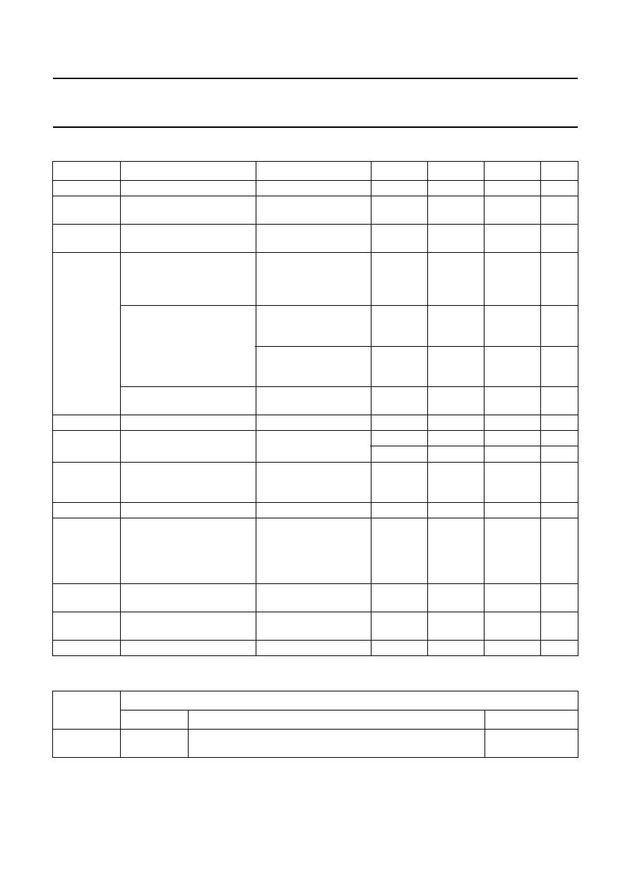
QUICK REFERENCE DATA
5
ORDERING INFORMATION
SYMBOL
PARAMETER
CONDITIONS
MIN.
TYP.
MAX.
UNIT
V
DDD(tot)
total DC supply voltage
all supply pins
4.75
5
5.5
V
I
DDD(tot)
total DC supply current
maximum activity of the
DSP; f
xtal
= 36 MHz
-
160
200
mA
P
tot
total power dissipation
maximum activity of the
DSP; f
xtal
= 36 MHz
-
0.8
1.1
W
S/N
level ADC signal-to-noise
ratio
RMS value;
unweighted;
B = 0 to 29 kHz;
maximum input
48
54
-
dB
ADC signal-to-noise ratio
not multiplexed;
B = 19 kHz;
V
i
= 1 V (RMS)
81
85
-
dB
multiplexed;
unweighted;
B = 19 kHz; 1 V (RMS)
72
76
-
dB
ADC signal-to-noise ratio for
FM-RDS
RMS value; B = 6 kHz;
unweighted; f
c
= 57 kHz
56
-
-
dB
V
iFS
ADC full-scale input voltage
V
DDA1
= 4.75 to 5.5 V
1.05V
DDA1
1.1V
DDA1
1.15V
DDA1
V
THD
total harmonic distortion
pins 62 and 71 to 75
f
i
= 1 kHz;
V
i
= 1 V (RMS)
-
-
71
-
61
dB
-
0.03
0.09
%
V
imc(rms)
maximum conversion input
voltage level pins 62 and
71 to 75 (RMS value)
THD < 1%
1.1
-
-
V
RES
DAC resolution
-
18
-
bits
(THD + N)/S
total harmonic distortion plus
noise-to-signal ratio for DAC
and operational amplifiers
R
L
> 5 k
AC;
R
fb
= 2.7 k
; f
i
= 1 kHz;
R
ref
= 18 k
;
V
oFS
= 2.8 V (p-p);
maximum I
2
S-bus signal
-
-
70
-
60
dB
DR
dynamic range of DAC
f
i
= 1 kHz;
-
60 dB;
A-weighted
92
102
-
dB
DS
digital silence of DAC
f
i
= 20 Hz to 17 kHz;
A-weighted
-
-
110
-
100
dB
f
xtalDSP
crystal frequency DSP part
-
36.86
-
MHz
TYPE
NUMBER
PACKAGE
NAME
DESCRIPTION
VERSION
SAA7707H
QFP80
plastic quad flat package; 80 leads (lead length 1.95 mm);
body 14
◊
29
◊
2.8 mm
SOT318-2

1997
May
30
5
Philips Semiconductors
Preliminary specification
Car radio Digital Signal Processor (CDSP)
SAA7707H
This text is here in white to force landscape pages to be rotated correctly when browsing through the pdf in the Acrobat reader.This text is here in
_
white to force landscape pages to be rotated correctly when browsing through the pdf in the Acrobat reader.This text is here inThis text is here in
white to force landscape pages to be rotated correctly when browsing through the pdf in the Acrobat reader. white to force landscape pages to be ...
6
BLOCK DIAGRAM
handbook, full pagewidth
ANALOG
SOURCE
SELECTOR
DIGITAL
SIGNAL
PROCESSOR
4
AM
62
MPXRDS
80
VrefRDS
70
VrefMPX
78
VDACNM
77
VDACPM
3
FM
72
AUXR
74
TAPER
73
TAPEL
71
AUXL
75
AMAF
76
FMMPX
79
FMRDS
RDS
DECODER
I
2
C-BUS
INTERFACE
ADC
ADC
ADC
INTERFERENCE
ABSORPTION
CIRCUIT
DIGITAL
STEREO
DECODER
SIGNAL
QUALITY
SIGNAL
LEVEL
DIGITAL
SOURCE
SELECTOR
DIGITALLY
CONTROLLED
SAMPLING
QUADRATURE
DAC
18
FIOL
13
Iref(int)
20
Vref
40
EXCLK
19
FVOL
16
FIOR
17
FVOR
11
12
9
RIOR
10
RVOR
RIOL
RVOL
21
POM
EXDAT2
EXDAT
TEST1
DCCCLK
DCCDAT
EXWS
EXDAT1
EXSCL
VSSD10
TEST2
DCCWS
CDDAT
CDWS
CDCLK
XTALI
XTALO
RDSDAT
RDSCLK
VDDX
VSSX
TSCAN
RTCB
SHTCB
DSPRESET
26
39
38
37
27
28
36
35
58
57
59
46
47
48
25
24
23
63
64
61
60
65
66
33 30
32
31
A0
SDA
SCL
VDDD1
7
VSSA
6
VDDO
15
VDDA1
69
MSS/P
43
DEEM
45
VDDD5
53
VDDD3
49
VSSD9
29
5
VSSD1
14
VSSO
8
VDDA
42
STEREO
44
MUTE
52
VDDD4
56
VDDD2
41
VSSD8
VSSD7
34
55
VSSD6
VSSD5
54
VSSD3
50 51
VSSD4
VSSD1
5
22
VSSD2
VSSG
67 68
VSSA1
CINT
2
1
VDACNL
CRYSTAL
OSCILLATOR
MBH163
SAA7707H
Fig.1 Block diagram.
1997 May 30
6
Philips Semiconductors
Preliminary specification
Car radio Digital Signal Processor (CDSP)
SAA7707H
7
PINNING
SYMBOL
PIN
I/O
DESCRIPTION
V
DACNL
1
-
internal ground reference voltage for the level ADC
CINT
2
level ADC switch-mode integrator connector
FM
3
I
FM level input; via this pin, the level of the received FM radio signal is fed to the
CDSP, the level information is required to enable correct functioning of the weak
signal behaviour
AM
4
I
AM level input; via this pin, the level of the received AM radio signal is fed to the
CDSP
V
SSD1
5
-
ground supply 1 for the DACs digital circuitry
V
SSA
6
-
ground supply for the DACs analog circuitry
V
DDD1
7
-
positive supply 1 for the DACs digital circuitry
V
DDA
8
-
positive supply for the DACs analog circuitry
RIOR
9
O
analog audio current output for rear right speaker
RVOR
10
O
analog audio voltage output for rear right speaker
RIOL
11
O
analog audio current output for rear left speaker
RVOL
12
O
analog audio voltage output for rear left speaker
I
ref(int)
13
I
internal reference current source input for the DACs
V
SSO
14
-
ground supply for DAC output operational amplifiers
V
DDO
15
-
positive supply for DAC output operational amplifiers
FIOR
16
O
analog audio current output for front right speaker
FVOR
17
O
analog audio voltage output for front right speaker
FIOL
18
O
analog audio current output for front left speaker
FVOL
19
O
analog audio voltage output for front left speaker
V
ref
20
I
voltage input for the internal reference buffer amplifier of the DAC
POM
21
activates the Power-on mute; timing is determined with an external capacitor
V
SSD2
22
-
ground supply 2 for the digital circuitry
CDCLK
23
I
clock input for CD digital audio source (I
2
S-bus)
CDWS
24
I
Word Select input for CD digital audio source (I
2
S-bus)
CDDAT
25
I
left/right data input for CD digital audio source (I
2
S-bus)
DSPRESET
26
I
input to reset DSP core (active LOW)
EXDAT1
27
I
external input data channel 1 (front) from extra DSP chip (I
2
S-bus)
EXDAT2
28
I
external input data channel 2 (rear) from extra DSP chip (I
2
S-bus)
V
SSD9
29
-
ground supply 9 for the digital circuitry
TSCAN
30
scan control (active HIGH)
A0
31
I
2
S-bus selection for slave sub-address
RTCB
32
asynchronous reset test control block (active HIGH)
SHTCB
33
shift clock test control block (active HIGH)
V
SSD7
34
-
ground supply 7 for the digital circuitry
EXDAT
35
O
output data for extra external DSP chip (I
2
S-bus)
EXSCL
36
O
output clock for extra external DSP chip (I
2
S-bus)
EXWS
37
I/O
word select input/output for extra external DSP chip (I
2
S-bus)
1997 May 30
7
Philips Semiconductors
Preliminary specification
Car radio Digital Signal Processor (CDSP)
SAA7707H
SCL
38
I
serial clock input (I
2
C-bus)
SDA
39
I/O
serial data input/output (I
2
C-bus)
EXCLK
40
I
external reference clock input to generate 4f
as
and f
as
synchronization; to be
used if the I
2
S-bus inputs are not suitable
V
SSD8
41
-
ground supply 8 for the digital circuitry
STEREO
42
FM stereo indication (active HIGH)
MSS/P
43
FM pause detector/MSS detector (active HIGH); also for IAC trigger output
MUTE
44
I
MUTE input pin (active LOW); only for FM mode
DEEM
45
de-emphasis; CD and DCC (active HIGH) (I
2
S-bus)
DCCCLK
46
I
DCC digital audio source clock input (I
2
S-bus)
DCCWS
47
I
DCC digital audio source Word Select input (I
2
S-bus)
DCCDAT
48
I
DCC digital audio source left/right data input (I
2
S-bus)
V
DDD3
49
-
positive supply 3 for the digital circuitry
V
SSD3
50
-
ground supply 3 for the digital circuitry
V
SSD4
51
-
ground supply 4 for the digital circuitry
V
DDD4
52
-
positive supply 4 for the digital circuitry
V
DDD5
53
-
positive supply 5 for the digital circuitry
V
SSD5
54
-
ground supply 5 for the digital circuitry
V
SSD6
55
-
ground supply 6 for the digital circuitry
V
DDD2
56
-
positive supply 2 for the digital circuitry
TEST1
57
test pin 1 (this pin should be left open-circuit)
V
SSD10
58
-
ground supply 10 for the digital circuitry
TEST2
59
test pin 2 (this pin should be left open-circuit)
RDSCLK
60
I/O
radio data system bit clock input/output
RDSDAT
61
O
radio data system data output
MPXRDS
62
I
in FM mode, selects between FMMPX and RDSMPX input signal to the MPX
decimation filter
XTALI
63
I
crystal oscillator input; can also be used as forced input in slave mode
XTALO
64
O
crystal oscillator output
V
DDX
65
-
positive supply crystal circuitry
V
SSX
66
-
ground supply crystal circuitry
V
SSG
67
-
ground guards for ADCs
V
SSA1
68
-
analog ground supply for ADCs
V
DDA1
69
-
analog positive supply for ADCs
V
refMPX
70
I
common mode reference voltage input for MPX ADC and buffers
AUXL
71
I
analog input for auxiliary left signal
AUXR
72
I
analog input for auxiliary right signal
TAPEL
73
I
analog input for tape left signal
TAPER
74
I
analog input for tape right signal
AMAF
75
I
analog input for AM audio frequency
FMMPX
76
I
analog input for FM multiplex signal
SYMBOL
PIN
I/O
DESCRIPTION

1997 May 30
8
Philips Semiconductors
Preliminary specification
Car radio Digital Signal Processor (CDSP)
SAA7707H
V
DACPM
77
I
supply voltage for the DACs switch capacitor of the FMMPX ADC and
FMRDS ADC
V
DACNM
78
I
ground supply for the DACs switch capacitor of the FMMPX ADC and
FMRDS ADC
FMRDS
79
I
analog FMMPX input for RDS decoding
V
refRDS
80
I
common mode reference voltage input for RDS ADC, level ADC and buffers
SYMBOL
PIN
I/O
DESCRIPTION

1997 May 30
9
Philips Semiconductors
Preliminary specification
Car radio Digital Signal Processor (CDSP)
SAA7707H
Fig.2 Pin configuration.
handbook, full pagewidth
SAA7707H
MBH162
1
2
3
4
5
6
7
8
9
10
11
12
13
14
15
16
17
18
19
20
60
59
58
57
56
64
63
62
61
55
54
53
52
51
50
49
48
47
46
45
44
43
42
41
21
22
23
24
25
26
27
28
29
30
31
32
33
34
35
36
37
38
39
40
80
79
78
77
76
75
74
73
72
71
70
69
68
67
66
65
VDACNL
VSSD1
VDDD1
VDDA
VSSA
CINT
FM
AM
RIOR
FIOR
POM
CDWS
CDDAT
TSCAN
A0
RTCB
SHTCB
V
SSD7
DSPRESET
EXDAT1
EXDAT
EXSCL
EXWS
SCL
SDA
EXCLK
EXDAT2
V
SSD9
CDCLK
RVOR
FVOR
FIOL
FVOL
RVOL
Iref(int)
Vref
VSSO
VSSD2
VDDO
RIOL
VSSD8
STEREO
MSS/P
MUTE
DEEM
DCCCLK
DCCWS
DCCDAT
VDDD3
VSSD3
VSSD4
VDDD4
VDDD5
VSSD5
VSSD6
VDDD2
VSSD10
TEST1
TEST2
RDSCLK
RDSDAT
MPXRDS
XTALI
XTALO
V
DDX
V
SSX
V
SSG
V
SSA1
V
DDA1
V
refMPX
V
refRDS
AUXL
AUXR
TAPER
AMAF
FMMPX
V
DACPM
V
DACNM
FMRDS
TAPEL
1997 May 30
10
Philips Semiconductors
Preliminary specification
Car radio Digital Signal Processor (CDSP)
SAA7707H
8
FUNCTIONAL DESCRIPTION
8.1
Signal path for level information
An FM and AM level input is implemented for FM weak
signal processing [for AM, FM and RDS search purposes
(absolute level and multi-path)]. A DC input signal is
converted by a bitstream 1st-order Sigma-Delta
analog-to-digital converter and then filtered by a
decimation filter.
The input signal has to be obtained from the radio part.
Two different circuits for AM and FM reception are
possible:
1. A circuit with two separate input signals, one for FM
level and one for AM level
2. A combined circuit with AM and FM level information
on the FM level input. The AM level input can then be
connected to another signal, which can be converted
in the non-radio mode.
The input is selected via the input selector control register.
The input signal for level control must be in the range of
0 to 5 V. The 11-bit level ADC converts this input voltage
in steps with a resolution better than 10 mV over the 5 V
range. The tolerance on the gain is less than 10%.
The MSB is always logic 0, to represent a positive level.
The decimation filter reduces the bandwidth of the
incoming signal to a frequency range of 0 to 29 kHz, with
a resulting sampling frequency (f
s
) of 76 kHz.
The response curve is illustrated in Fig.3.
The level information is sub-sampled by the DSP core to
obtain a field strength and a multi-path indication.
These values are stored in the coefficient or data RAM.
They can be read and used in other microcontroller
programs via the I
2
C-bus.
8.2
Level ADC switch mode integrator (pin CINT)
The level ADC has an internal current summation point of
the input level and the switch capacitor DAC. When used
as an integrator, an external capacitor of 1000 pF should
be connected between this pin and the analog ground at
pin V
SSA1
. The summation voltage is used as an input for
the analog-to-digital comparator level.
8.3
Internal ground reference for the level ADC
(pin V
DACNL
)
This pin serves as the internal ground reference for the
switch capacitor DAC and the level ADC and has to be
connected to the analog ground (pin V
SSA1
).
Fig.3 Frequency response of the level ADC and decimation filter.
handbook, full pagewidth
80
10
-
60
0
(dB)
20
10
30
40
50
60
70
f (kHz)
MBH164
-
10
-
20
-
30
0
-
50
-
40

1997 May 30
11
Philips Semiconductors
Preliminary specification
Car radio Digital Signal Processor (CDSP)
SAA7707H
8.4
Common mode reference voltage for RDS
ADC, ADC level and buffers (pin V
refRDS
)
The middle reference voltage of the RDS ADC can be
filtered via this pin. This middle reference voltage is used
as a positive reference for the level ADC of the switch
capacitor DAC and as half supply reference for the RDS
ADC, the switch capacitor DACs and buffers. An external
capacitor (connected to V
SSA1
) prevents crosstalk
between the switch capacitor DACs of the RDS ADC, level
ADC and buffers, and improves the power supply rejection
ratio.
8.5
Signal path for audio/MPX and stereo decoder
The SAA7707H has four analog audio source inputs; two
single-multiplex channel inputs for AM and FM radio and
two stereo inputs for tape and auxiliary. The auxiliary input
can be used for functions such as an analog CD changer
or speech applications. The stereo inputs are multiplexed
so that they can share the same filters as the multiplexed
FM signal. The selection between the AM, FM, TAPE and
AUX input is made via the input selector control register.
The input signal behind the source selector is digitized by
a bitstream 3rd-order Sigma-Delta ADC. The first
decimation filter reduces the sample rate. This is followed
by the sample-and-hold switch of the IAC and the 19 kHz
regeneration circuit. From here, the wide-band noise
detector signal HP2 (High-Pass 2) with a frequency range
of 60 to 240 kHz is derived. A second decimation filter
reduces the output of the IAC to a lower sample rate.
This filter has two outputs, one for the multiplex signal with
a frequency range of 0 to 60 kHz (low-pass) and one for
the small-band noise detector signal HP1 (High-Pass 1)
with a frequency range of 60 to 120 kHz. The overall
low-pass frequency response of the decimation filters is
illustrated in Fig.4.
In the FM mode, the RDS ADC can be used as an input for
the MPX decimation filter. This can be selected via the
RDSMPX input at pin 62.
The outputs from this signal path to the DSP, which are all
at a sample frequency of 38 kHz, are as follows:
∑
Pilot presence indication: Pilot-I. This 1-bit signal is
LOW for a pilot frequency deviation of less than 4 kHz
and HIGH for a pilot frequency deviation greater than
4 kHz. It is AND locked on a pilot tone.
∑
Pilot quality indication: Pilot-Q. This 10-bit signal
contains information about the signal quality and is
derived from the quadrature component of the pilot-I
signal.
∑
`Left' and `Right': This is the 18-bit output of the stereo
decoder after the matrix decoding. For AM reception,
the `Right' signal contains the AM-mono signal. For tape
or auxiliary signals, the output of the stereo decoder
contains sum and difference signals, but with other
crosstalk properties than on FM. Therefore, a different
matrix correction, as shown in Table 1, has to be applied
to these signals in the DSP program. The overall
frequency response of the demultiplexed signal at the
output of the stereo decoder is illustrated in Fig.5.
Table 1
Overview of the signals to the CDSP
Apart from the aforementioned theoretical response, the
non-flat frequency response of the ADC must also be
compensated for in the DSP program.
8.6
Mono/stereo switching
After division, the Digitally Controlled Sampling (DCS)
clock generates a clock signal with a frequency which is a
multiple of 19 kHz plus or minus a few Hertz. For mono
reception, the DCS circuit generates a preset frequency of
n
◊
19 kHz
±
2 Hz. For stereo reception, the frequency is
exactly n
◊
19 kHz (DCS locked to n
◊
pilot tone).
The detection of the pilot and the stereo indication is
performed in the DSP program.
8.7
The automatic lock system
The VCO operates at 19 kHz
±
2 Hz exactly for no-pilot.
For stereo reception, the phase error is zero for a pilot tone
with a frequency of exactly 19 kHz. Therefore, no switch is
required to preset the clock to 19 kHz. With auxiliary
sources (tape, CD, etc.), the DCS circuit has to be preset
to a fixed value.
8.8
Input sensitivity for FM
The FM input sensitivity is optimally designed for an FM
front-end with an output voltage of 200 mV (RMS) at a
modulation depth of 22.5 kHz of a 1 kHz tone. Due to the
full-scale 1.2 V (RMS) handling capacity of the ADC, the
maximum allowed modulation depth of a transmitter, for a
THD of 10%, is 135 kHz. Full performance is possible for
transmitters with a modulation depth of up to 110 kHz.
MODE
LEFT
RIGHT
AM
0
mono
FM
1
/
2
(R
-
L)
R
+
L
TAPE/AUX
1
/
2
(R
+
L)
◊
4/
R
+
L
1997 May 30
12
Philips Semiconductors
Preliminary specification
Car radio Digital Signal Processor (CDSP)
SAA7707H
Fig.4 Overall frequency response multiplex ADC and decimation filters.
handbook, full pagewidth
500
400
450
10
0
-
110
-
130
-
150
0
(dB)
100
50
150
200
250
300
350
f (kHz)
MBH165
-
10
-
30
-
50
-
90
-
70
Fig.5 Transfer of MPX signal at the output of the stereo decoder.
handbook, full pagewidth
80
20
-
60
-
100
-
80
0
(dB)
20
10
30
40
50
60
70
f (kHz)
MBH166
-
20
0
-
40

1997 May 30
13
Philips Semiconductors
Preliminary specification
Car radio Digital Signal Processor (CDSP)
SAA7707H
8.9
Common mode reference voltage for MPX ADC
and buffers (pin V
refMPX
)
The middle reference voltage of the MPX ADC can be
filtered via this pin. This middle reference voltage is used
as a half supply voltage reference for the MPX ADC,
switch capacitor DACs and buffers. An external capacitor
(connected to V
SSA1
) prevents crosstalk between the
switch capacitor DACs and buffers and improves the
power supply rejection ratio.
8.10
Supply voltages for the switch capacitor DACs
of the FMMPX ADC and FMRDS ADC
(pins V
DACNM
and V
DACPM
)
These pins are used as ground and positive supply voltage
reference for the MPX ADC, RDS ADC and the switch
capacitor DACs. For optimum performance they must be
connected directly to V
SSA1
and V
DDA1
.
8.11
Noise level
The High-Pass 1 (HP1 or narrow-band noise level filter)
output of the second MPX decimation filter, in a frequency
band from 60 to 120 kHz, is detected with an envelope
detector and decimated to a frequency of 38 kHz.
The response time of the detector is 100 ms.
Another option is the High-Pass 2 (HP2 or wide-band
noise level filter). This output from the first MPX decimation
filter is in a frequency band from 60 to 240 kHz. It has the
same properties as the HP1 and is also decimated to
38 kHz. Which signal is used (HP1 or HP2) is determined
by the input selector control register. The noise level can
be detected and filtered in the DSP core and can be used
to optimize the FM weak-signal processing. The transfer
curves of both filters before decimation are illustrated in
Fig.6.
Fig.6 Frequency response of noise level before decimation.
handbook, full pagewidth
10
0
-
110
-
130
-
150
0
(dB)
100
50
150
200
250
300
350
f (kHz)
MBH167
-
10
-
30
-
50
-
90
-
70
(1)
(2)
(1) Narrow-band noise level filter.
(2) Wide-band noise level filter.
1997 May 30
14
Philips Semiconductors
Preliminary specification
Car radio Digital Signal Processor (CDSP)
SAA7707H
8.12
TAPE/AUX de-multiplex
The auxiliary and tape inputs also use the stereo decoder.
Because of this, the left and right channels are multiplexed
with a 38 kHz square wave to obtain a signal similar to the
FM multiplexed signal. Auxiliary inputs can be e.g.
TV-sound, remote players (tape deck, CD-changer with
analog output etc.). The signal-to-noise ratio from such
sources is limited by the ADC in the SAA7707H (>75 dB).
The decimation filter of the ADC attenuates the harmonic
signals from this stereo encoder. For an optimum channel
separation, the 38 kHz switch signal has to be phase
corrected to compensate for the delay of the ADC and
decimation filters. This can be adjusted with the 3-bit group
delay compensation in the IAC control register. Signal
frequencies above 19 kHz at the input of the multiplexer
are converted to the audio base-band and are therefore
not allowed.
8.13
Signal-to-noise considerations
Due to the pre-emphasis of FM broadcasts, the theoretical
signal-to-noise ratio is approximately 3 dB higher for FM
stereo in comparison with multiplexed inputs.
To avoid aliasing into the tape channel, the tape noise from
the pre-amplifier must be attenuated before
analog-to-digital conversion with a 1st-order 10 kHz
low-pass filter. The frequency response is equalized after
the stereo decoder in the DSP program before the Dolby
decoder software. Using this filter, the signal-to-noise ratio
of this channel is degraded by 3 dB. This results in a
signal-to-noise ratio that is overall 6 dB lower than a tape
input with respect to FM stereo.
8.14
Channel separation correction
The channel separation is approximately 50 dB at 1 kHz
and 35 dB at 15 kHz. Because the frequency response of
the ADC has some deviation from the flat curve around
38 kHz, a perfect channel separation cannot be obtained.
Therefore, the de-multiplexed signal is corrected for
crosstalk in the DSP program.
8.15
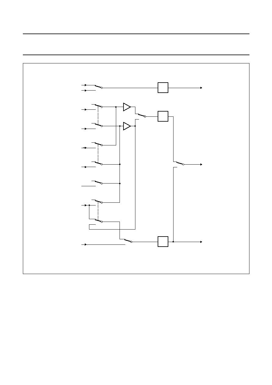
Input selection switches
A schematic diagram of the input selection is illustrated in
Fig.5. The input selection is controlled by bits in the input
selector control register. The relationship between these
bits and the switches is indicated in Table 2.
Table 2
Analog input selection
8.16
Analog inputs supply
The analog input circuit has its own separate power supply
connections to allow maximum filtering. These pins are
V
SSA1
for the analog ground and V
DDA1
for the analog
power supply. V
SSG
is the connection to the guard ring
which isolates the analog part from the digital filters.
This pin has to be connected to the analog ground.
8.17
Digitally controlled sampling clock (DCS)
The crystal clock generates a continuous clock signal for
the internal DSP core. In the radio mode, the stereo
decoder, the RDS decoder, the ADCs and the level
decimation filters have to run synchronously with the
19 kHz pilot. Therefore, a clock signal with a controlled
frequency with a multiple of 19 kHz
(9.728 MHz = 512
◊
19 kHz) is required.
In the SAA7707H, the patented method of a
non-continuous digitally controlled sampling clock has
been implemented. A frequency of 9.728 MHz is
generated by a special dividing mechanism of the master
crystal clock. Since the dividing mechanism is fixed, only a
crystal frequency of 36.86 MHz can be used.
The DCS system is controlled by up/down information
from the stereo decoder. For mono transmissions, the
DCS clock is still controlled by the stereo decoder loop.
The output keeps the DCS free-running at a multiple
frequency of 19 kHz
±
2 Hz. In TAPE/AUX and AM mode,
the DCS clock must always be put in preset mode by the
input selector control register.
I
2
C-BUS SELECTION
BIT
SWITCH
AM/FM
AUX/
RADIO
TAPE/
AUX
SFM SAM SAUX SAUX
0
0
x
1
0
0
0
1
0
x
0
1
0
0
x
1
0
0
0
1
0
x
1
1
0
0
0
1
1997 May 30
15
Philips Semiconductors
Preliminary specification
Car radio Digital Signal Processor (CDSP)
SAA7707H
8.18
Survey of the DCS clock settings in different
modes
The DCS clock behaves as shown in Table 3.
Table 3
DCS clock/mode
8.19
Synchronization with the core
A 38 kHz synchronization signal is derived from the DCS
clock and divided by 256.
If the external I
2
S-bus DCC CD is selected, the rising edge
of the Word Select input signal is used to synchronize with
the core.
MODE
DCS CLOCK
FM stereo
locked on 19 kHz pilot of received
FM signal
FM mono
free running
AM analog inputs
TAPE/AUX
fixed preset
I
2
C-bus inputs
DCC/CD
fixed preset
8.20
Interference absorption circuit
The Interference Absorption Circuit (IAC) detects and
suppresses ignition interference. This hardware IAC is a
modified and digital version of the analog circuit that has
already been in use for many years.
The input signal to the IAC circuit is derived from the output
signal of the decimation filter. The interference detector
analyses the high frequency content of this MPX signal.
The discrimination between interference pulses and other
signals is performed by a special Philips patented fuzzy
logic-like algorithm and is based on probability
calculations. This logic will send appropriate pulses to an
MPX mute switch.
At Power-on, the nominal setting for an IAC with good
performance characteristics is selected (all IAC control bits
are 0). If an adjustment is needed, the characteristics can
be adapted as described in the application manual.
8.21
IAC testing
The internal IAC trigger signal is visible on the MSS/P pin
(pin 43) if the IAC trigger output bit of the IAC control
register is set. In this mode, the effect of the parameter
settings on the IAC performance can be verified.
1997 May 30
16
Philips Semiconductors
Preliminary specification
Car radio Digital Signal Processor (CDSP)
SAA7707H
∑
The SAMFM switch is controlled by the SEL-LEV-AM/FM bit
∑
The SINTEXT switch is controlled by the SEL-RDS-EXT/INT bit
∑
The CLMPX switch is controlled by the 38 kHz clock derived from the DCS, but is not active in FM and AM mode.
In the FM radio mode, the MPXRDS pin overrides the following switches when set to logic HIGH:
If SEL-AM/FM = 0 and SEL-AUX/RADIO = 0 and pin MPXRDS = 1, then SFM = 0, SINTEXT = 1 and MPXRDS = 1.
Fig.7 Schematic diagram of input selection.
handbook, full pagewidth
MBH168
ADC
CLMPX
SAMFM
0
1
0
1
0
1
RDS_MPX
0
1
ADC
TAPER
0
1
AM
FM
TAPEL
0
1
0
1
AUXR
0
1
AM/FM
AUXL
level
SINTEXT
ADC
0
1
FMRDS
RDS
MPX
STAPE
SAUX
0
1
0
1
FMMPX
SFM
SAM

1997 May 30
17
Philips Semiconductors
Preliminary specification
Car radio Digital Signal Processor (CDSP)
SAA7707H
9
ANALOG OUTPUTS
9.1
Digital-to-analog converters
Each of the four low-noise high dynamic range DACs
consists of a 15-bit signed magnitude DAC with current
output, followed by a buffer operational amplifier.
The five higher bits (bits 10 to 14) are used to control the
total coarse current ratio of the 32 coarse current sources
via a thermometer decoder. The nine lower bits
(bits 1 to 9) are derived from a 512 transistor matrix, which
acts as a passive 9-bit current divider for one of the coarse
currents. The MSB (bit 15) is used as a sign bit for the
signed magnitude converter and controls the direction of
the total output current. A separate converter is used for
each of the four audio output channels. The value of each
coarse current is adjusted by the current through the
external resistor connected to pin 13 (I
ref(int)
).
Each converter output is connected to the inverting input
of one of the four internal CMOS operational amplifiers.
The non-inverting input of this operational amplifier is
connected to the internal reference voltage. Together with
an external resistor, the current-to-audio output voltage
conversion is achieved.
9.2
Upsample filter
To reduce spectral components above the audio band, a
fixed 4 times oversampling and interpolating 18-bit digital
IIR filter is used. It is realized as a bit serial design and
consists of two consecutive filters. The data path in these
filters is 22 bits, to prevent overflow and to maintain a
theoretical signal-to-noise ratio greater than 105 dB.
The filters give an attenuation of at least 29 dB. The filter
is followed by a 5 bit 1st-order noise shaper, to expand the
dynamic range to more than 105 dB.
The band around multiples of the sample frequency of the
DAC (4f
as
) is not affected by the digital filter. A capacitor
can be added in parallel with the output resistor at the DAC
output to further attenuate this out-of-band noise to an
acceptable level.
The overall frequency spectrum at the DAC audio output
without external capacitor/low-pass filter for the audio
sampling frequencies (f
as
) of 38 kHz is illustrated in Fig.8.
The detailed spectrum around f
as
is illustrated in Fig.9 for
an f
as
of 38 kHz, 44.1 kHz and 48 kHz. The pass-band
bandwidth (at
-
3 dB) is
1
/
2
f
as
.
The word clock for the upsample filter (4f
as
) is derived from
the audio source timing. If the internal audio source is
selected, the sample frequency is fixed at 38 kHz.
For external digital sources (DCC and CD), a sample
frequency from 32 to 48 kHz is possible. The sample
frequency is automatically adjusted to the I
2
S-bus input by
dividing the external bit clock. This clock is normally
present in a DCC CD application. An internal digital PLL
divides this clock with the integer factor needed to obtain
the 4f
as
word clock. Master synchronization of this divided
clock signal is obtained with a reset of the divider on the
Word Select signal (trailing edge) of the I
2
S-bus.
In the application, the I
2
S-bus signal from the external
source should fulfil the following requirements:
∑
There is a continuous (is part of the basic I
2
S-bus
specification) n
◊
4f
as
(4
<
n
<
128) I
2
S-bus bit clock or
∑
If the I
2
S-bus bit clock is not continuous, another n
◊
4f
as
(4
<
n
<
128) continuous clock signal has to be
connected to the EXCLK pin (pin 40). The divide
external clock mode has to be selected using the input
selector control register.
The range of the internal 7-stage programmable divider of
the PLL, to obtain 4f
as
, is large enough to handle 16-bit
I
2
S-bus signals as well as master clocks up to 22 MHz
from digital sources (CD, DCC, R-DAT and EBU interface)
without any clock regeneration.
The PLL is used in a free-running mode to ensure that jitter
on the I
2
S-bus signals (due to asynchronous clocking of
the I
2
S-bus signals by the DSP core) will not influence the
total harmonic distortion of the audio signal on the analog
DAC part. This will, however, only operate if there is no
jitter on the bit clock or when a crystal clock is used.
9.3
Volume control
The total volume control has a dynamic range of more than
100 dB. With the signed magnitude noise-shaped 15-bit
DAC and the internal 18 bit registers of the DSP core, a
useful digital volume control range of 100 dB is possible by
calculating the corresponding coefficients. The step size is
freely programmable and an additional analog volume
control is not needed in this design. The signal-to-noise
ratio of the audio output, at full-scale, is determined by the
total 15 bits of the converter.
The noise at low outputs is fully determined by the noise
performance of the DAC. Since it is a signed magnitude
type, the noise at digital silence is also low.
The disadvantage is that the total THD is higher than
conventional DACs. The typical signal and noise levels as
a function of the output level and the typical signal-to-noise
plus THD as a function of the output level are illustrated in
Fig.10.

1997 May 30
18
Philips Semiconductors
Preliminary specification
Car radio Digital Signal Processor (CDSP)
SAA7707H
9.4
Power-on mute
To avoid any uncontrolled noise at the audio outputs after
Power-on of the IC, the reference current source of the
DAC is switched off. The capacitor connected to pin 21
(POM) determines the time after which this current has a
soft switch-on. Consequently, at Power-on, the current
audio signal outputs are always muted. The voltage output
signals will show a small jump at switch-on due to the
asymmetrical voltage supply of the output operational
amplifiers. These types of disturbances must be
eliminated via the application set-up. The output has to be
set to digital silence before the POM pin is at logic HIGH.
This is achieved via the DSP program control and/or a zero
volume setting. The pin is internally connected to V
DDO
with a high-ohmic resistor.
9.5
Power-off plop suppression
To avoid plops in a power amplifier, the supply voltage of
the analog part of the DAC can be fed via a Schottky diode
and an extra capacitor. In this situation, the output voltage
will decrease gradually, allowing the power amplifier some
extra time to switch off without audible plops.
9.6
Internal reference buffer amplifier of the DAC
(pin V
ref
)
Using two internal resistors, half of the supply voltage
(V
DDO
) is obtained and coupled to an internal buffer.
This reference voltage is used as a DC voltage for the
output operational amplifiers and as a reference voltage
for the DAC. In order to obtain the lowest noise and to have
the best ripple rejection, a filter capacitor has to be added
between this pin and ground.
9.7
Internal DAC current reference
As a reference for the current at the DAC current source,
a current is drawn from pin 13 (I
ref(int)
) to the V
SSO
ground.
The voltage at this pin is
1
/
2
V
DDO
(typically 2.5 V).
The maximum DAC current is equal to 4.5 times this
current. When a reference resistor of 18 k
is used, the
reference current from the DAC is 125
µ
A. This results in
a peak current from the four current outputs of
4.5
◊
125 = 562.5
µ
A.
9.8
Analog outputs supply
For an optimum signal-to-noise performance, supply ripple
rejection and to suppress switch-off plops, the output
operational amplifiers, the analog part of the DACs and the
upsample filter plus digital part have separate power
supply connections.
The operational amplifiers have the V
SSO
and V
DDO
pins
as ground and positive supply. These pins also provide the
supply for the reference circuits. The analog DAC part
uses the V
SSA
and V
DDA
pins as ground and positive
supply. The upsample filter and digital part of the DAC
share the V
SSD1
and V
DDD1
as ground and positive supply
connections.
9.9
Clock circuit and oscillator
The SAA7707H has an on-board crystal clock oscillator.
The schematic of this Pierce oscillator is illustrated in
Fig.11. The active element needed to compensate for the
loss resistance of the crystal is the block `Gm'. This block
is placed between the XTAL (output) and the OSC (sense)
pins. The gain of the oscillator is internally controlled by the
AGC block; this prevents excessive power loss in the
crystal. The higher harmonics are then as low as possible.
The signal on the XTAL pin is amplified and divided by two.
This 18.43 MHz signal is then used as the DSP clock
signal (PH2). For the high frequency, as used in the
SAA7707H, normally only third overtone crystals are
available. With an external LC notch filter at the
fundamental frequency, oscillation at this frequency can
be avoided.The crystal frequency is chosen in such a way
that the harmonics are outside the normal FM band.
The crystal frequency used is 36.86 MHz.
9.10
Crystal oscillator supply
The power supply connections for the oscillator are
separate from the other supply lines. This is to minimize
the feedback from the ground bounce of the chip to the
oscillator circuit. The V
SSX
pin (pin 66) is used as ground
supply and the V
DDX
pin (pin 65) as positive supply.
9.11
External control pins
For external control, two input pins have been
implemented. The status of these pins can be changed by
applying a logic level, and is recorded in the internal status
register. The functions of each pin are as follows:
∑
MUTE (pin 44). Mute input (0 = MUTE)
∑
DEEM (pin 45). This pin activates the de-emphasis for
CD and DCC. (1 = de-emphasis on).
To control external devices, two output pins are
implemented. The status of these pins is controlled by the
DSP program. The functions of each pin are as follows:
1997 May 30
19
Philips Semiconductors
Preliminary specification
Car radio Digital Signal Processor (CDSP)
SAA7707H
∑
STEREO (pin 42): Indicates whether an FM broadcast is in stereo (1 = stereo)
∑
MSS/P (pin 43): Indicates a pause in FM or tape search mode (1 = pause). This is also the IAC trigger output for IAC
alignment if the corresponding I
2
C-bus bit is set.
handbook, full pagewidth
500
400
450
0
-
45
-
55
-
65
0
(dB)
100
50
150
200
250
300
350
f (kHz)
MBH169
5
-
5
-
15
-
35
-
25
Fig.8 Overall frequency spectrum audio output (f
as
= 38 kHz).
Fig.9 Detailed frequency spectrum of audio output.
handbook, full pagewidth
40000
10
0
(dB)
10000
20000
30000
46420
0
11605
23211
34815
50528
0
12632
25263
37895
f (Hz)
MBH170
-
10
-
20
-
30
0
-
50
-
40
1997 May 30
20
Philips Semiconductors
Preliminary specification
Car radio Digital Signal Processor (CDSP)
SAA7707H
Fig.10 Typical signal-to-noise level and signal-to-noise plus THD as a function of output level.
handbook, full pagewidth
0
-
10
-
20
-
30
-
40
-
50
-
60
-
70
-
80
-
90
-
100
0
20
40
60
80
100
S/(N
+
THD)
and
S/N (dB)
output level (dB)
MBH171
(1)
(2)
(1) Signal-to-noise.
(2) Signal-to-noise + total harmonic distortion.
Fig.11 Schematic diagram of the oscillator circuit.
handbook, full pagewidth
MBH172
Gm
63
64
65
66
XTAL
OSC
VDDX
VSSX
AGC
Rbias
/2
PH2
C x 1
C x 2
ON CHIP
OFF CHIP

1997 May 30
21
Philips Semiconductors
Preliminary specification
Car radio Digital Signal Processor (CDSP)
SAA7707H
10 I
2
S-BUS DESCRIPTION
10.1
I
2
C-bus control (pins SCL and SDA)
For external control of the SAA7707H, a standard I
2
C-bus
is implemented. There are two different types of control
instructions:
∑
Instructions to control the DSP program, programming
the coefficient RAM and reading the values of
parameters (level, multi-path etc.)
∑
Instructions controlling the DATA flow, such as source
selection, IAC control and clock speed.
10.2
I
2
S-bus description
For communication with external digital sources and/or
additional external processors, the I
2
S-bus digital interface
is used. It is a serial 3-line bus, having one line for Serial
Data (SD), one line for Serial Clock (SCK) and one line for
the Word Select (WS). For external processors, the CDSP
acts as a master transmitter; for external digital sources
the CDSP acts as a slave. The communication with the
external processor and external digital sources are
separated, to allow both features at the same time.
Figure 12 shows an extract of the Philips I
2
S-bus
specification interface report regarding the general timing
and format of the I
2
S-bus. Word select logic 0 means left
channel word; word select logic 1 means right channel
word.
The serial data is transmitted in twos complement with the
MSB first. One clock period after the negative edge of the
Word Select line, the MSB of the left channel is
transmitted. Data is synchronized with the negative edge
of the clock and latched at the positive edge.
As inputs from an external processor for the four audio
channels, two data lines have been implemented.
10.3
Communication with external digital audio
sources (DCC + CD-WS/CL/Data pins)
For communication with external digital audio sources, two
additional I
2
S-bus inputs are available. They each have
clock, data and Word Select input lines with a maximum
useful data length of 18 bits. The external source is master
and supplies the clock. The input selection and port
selection is controllable via the input selector control
register. The DSP program is synchronized with the
external source via the Word Select signal.
The input allows a variety of clock frequencies, sample
frequencies and word lengths.
The Word Select line automatically determines the
SAA7707H sampling frequency.
Using the Digital Source Selector (see Fig.1), one of the
three possible input sources is selected. The selected
audio data channels are input to two 18-bit wide memory
mapped I/O registers of the DSP named Input Left and
Input Right.
Except for the 4f
as
pulse to control the upsample filter
(see Section 9.2), other synchronization signals such as
internal Word Select are derived from the I
2
S-bus input
signals.
The input bit clock is used as a bit clock for the external
processor. As a consequence, a clock pulse input signal
with less than 18 bits will result in a communication with an
external processor of the same number of bits. In this
event, the trailing bits of the 18-bit input registers will be
zero.
If the I
2
S-bus driver outputs of the external digital source
ICs have 3-state outputs, they can all be connected on one
single I
2
S-bus input.
10.4
Communication with external processors and
other devices (EXWS/CL/EXDAT1 and EXDAT2)
For communication with external processors, delay lines
or other I
2
S-bus controllable devices, a complete
dual-channel 18-bit output bus is implemented.
The SAA7707H acts as the master transmitter and the
external device has to be synchronized with the Word
Select line.
As input for the processed data, two data input lines have
been implemented that are processed synchronously with
the data output to the external processor (see Table 4).
This enables, in total, a feedback of two stereo audio
channels.
For this communication, the DSP core has the following
18-bit memory mapped I/O registers available:
Table 4
DSP core I/O registers
The DSP program moves data from the two external
I
2
S-bus data output registers to the external processor and
reads it back from the two or four external I
2
S-bus data
input registers. The hardware of the bus can be enabled by
the input control register.
INPUT
OUTPUT
EXDAT1 left/right
EXDAT left/right
EXDAT2 left/right

1997 May 30
22
Philips Semiconductors
Preliminary specification
Car radio Digital Signal Processor (CDSP)
SAA7707H
To minimise electro magnetic interference (EMI), the
output has to be disabled if the output is not used.
The timing diagram of the communication is illustrated in
Fig.13.
10.5
Relationship between external input and
external output
The stereo decoder output has an internal I
2
S-bus format
with 32 clock pulses per channel for 18 valid and 14 zero
data bits. Providing that the stereo decoder output is used,
the communication with the external processor will also
have 32 clock pulses per channel for 18 valid and 14 zero
data bits.
When an external digital source is selected, the number of
valid bits and clock pulses of this source determines the
output to the external processor. This relationship is
shown in Table 5.
Table 5
Relationship between external input and
external output.
10.6
RDS decoder (RDSCLK and RDSDAT)
The RDS decoder recovers the additional inaudible RDS
information transmitted by FM radio broadcasting.
The (buffered) data is provided as an output for further
processing by a suitable decoder. The operational
functions of the decoder are in accordance with EBU
specification
EN 50067.
The RDS decoder has three different functions:
1. Clock and data recovery from the MPX signal
2. Buffering of 16 bits, if selected
3. Interfacing with the microcontroller.
10.7
Clock and data recovery
The RDS chain has a separate input. This enables RDS
updates during tape play and also the use of a second
receiver for monitoring the RDS information of signals from
another transmitter (double tuner concept).
INPUT
CLOCK
BITS
INPUT
DATA
BITS
OUTPUT
CLOCK
BITS
OUTPUT
DATA
BITS
>32
18
32
18
18 and
32
18
as input
18
18 and
32
<18
as input
18
<18
<18
as input
as input
In this way, it can be performed without interruption of the
audio program. The MPX signal from the main tuner of the
car radio can be connected to this RDS input via the
built-in source selector.
The input selection is controlled by the input selector
control register.
For FM stereo reception, the clock of the total chip is
locked to the stereo pilot (19 kHz multiple). For FM mono,
the DCS loop keeps the DCS clock around the same
19 kHz multiple. In all other cases, such as AM reception
or tape, the DCS circuit has to be set to a preset position.
Under these conditions, the RDS system is always clocked
by the DCS clock in a 38 kHz (4
◊
9.5 kHz) based
sequence.
10.8
Timing of clock and data signals
The timing of the clock and data output is derived from the
incoming data signal. Under stable conditions, the data will
remain valid for 400
µ
s after the clock transition.
The timing of the data change is 100
µ
s before a positive
clock change. This timing is suitable for positive and
negative triggered interrupts on a microcontroller.
The RDS timing is illustrated in Fig.14.
During poor reception, it is possible that errors in phase
may occur. Consequently the duty cycle of the clock and
data signals will vary from a minimum of 0.5 times to a
maximum of 1.5 times the standard clock periods.
Normally, errors in phase do not occur on a cyclic basis.
10.9
Buffering of RDS data
The repetition frequency of RDS data is approximately
1187 Hz. This results in an interrupt on the microcontroller
every 842
µ
s. In a second mode, the RDS interface has a
double 16-bit buffer.
10.10 Buffer interface
The RDS interface buffers 16 data bits. Each time 16 bits
are received, the data line is pulled down and the buffer is
overwritten. The control microcontroller has to monitor the
input data line at least every 13.5 ms. This mode is
selected by the input selector control register.
The interface signals from the RDS decoder and the
microcontroller in the buffer mode are illustrated in Fig.15.
When the buffer is filled with 16 bits, the data line is pulled
down.
The data line will remain LOW until reading from the buffer
is started, by pulling down the clock line. The first data bit
is clocked out.
1997 May 30
23
Philips Semiconductors
Preliminary specification
Car radio Digital Signal Processor (CDSP)
SAA7707H
After 16 clock pulses, the buffer is read and the data line is
set HIGH until the buffer is filled again. The microcontroller
stops communication by pulling the clock line HIGH.
The data is written out just after the clock HIGH-to-LOW
transition. The data is valid when the clock is HIGH.
When a new 16-bit buffer is filled before the other buffer is
read from, that buffer will be overwritten and the old data
will be lost.
10.11 DSP reset
The reset pin (DSP) is active LOW and has an internal
pull-up resistor. To allow a proper switch-on of the supply
voltage, a capacitor should be connected between this pin
(pin 26) and V
SSD
. The value of the capacitor is such that
the SAA7707H will remain in reset as long as the power
supply is not stabilized. A more or less fixed relationship
between the DSP reset and the POM (pin 21) time
constant is obligatory. The voltage on the POM pin
determines the current flowing in the DACs. At 0 V
(at pin 21), the DAC currents are zero and therefore the
DACs output voltages are also zero. At 5 V, the DAC
currents are at their nominal (maximum) value.
Long before the DAC outputs reach their nominal output
voltages, the DSP must be in the working mode (to reset
the output register) therefore, the DSP time constant must
be shorter than the POM time constant. For advised
capacitors, see Figs. 24 and 25.
The DSP reset has the following functions:
∑
The bits of the IAC control register are set to logic 0
∑
The bits of the input selector control register are set to
logic 0
∑
The program counter is set to address $0000.
When the level on the DSP is at logic HIGH, the DSP
program starts to run.
10.12 Power supply connection and EMC
The digital part of the SAA7707H has 5 positive supply
lines (V
DDD1
to V
DDD5
) and 10 ground connections
(V
SSD1
to V
SSD10
). To minimize radiation, the SAA7707H
should be put on a double-layer PCB with, on one side, a
large ground plane. The ground supply lines should have
a short connection to this ground plane. A coil/capacitor
network in the positive supply line can be used as a high
frequency filter.
Fig.12 I
2
S-bus timing and format.
handbook, full pagewidth
Tcy
tLC
0.35 T
tsr
0.2 T
thr
0
tHC
0.35 T
VIH (70%)
VIL (20%)
VIH (70%)
VIL (20%)
SCK
MBH173
SD
SCK
WS
SD
WS
MSB
RIGHT
MSB
LEFT

1997 May 30
24
Philips Semiconductors
Preliminary specification
Car radio Digital Signal Processor (CDSP)
SAA7707H
Fig.13 Timing diagram of the CDSP to external processor.
handbook, full pagewidth
MBH174
ts2
tf
tr
tf
tr
td1
tf
tr
t3
ta
tHC
tLC
td2
EXDAT
OUTPUT
EXDAT1
EXDAT2
INPUT
WS
CL
EXDAT
EXWS
EXSCL
EXDAT1
EXDAT2
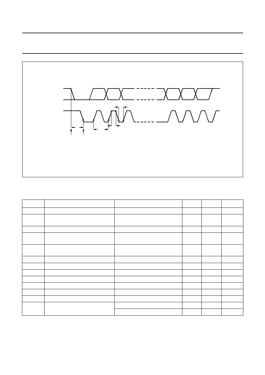
Fig.14 RDS timing diagram in direct output mode.
handbook, full pagewidth
MBH175
RDSDAT
RDSCLK
ts
tHC
tLC
td
Tcy
1997 May 30
25
Philips Semiconductors
Preliminary specification
Car radio Digital Signal Processor (CDSP)
SAA7707H
11 LIMITING VALUES
In accordance with the Absolute Maximum Rating System (IEC 134).
Notes
1. Human body model: C = 100 pF; R = 1500
; 3 pulses positive plus 3 pulses negative.
2. Machine model: C = 200 pF; L = 2.5
µ
H; R = 25
; 3 pulses positive plus 3 pulses negative.
SYMBOL
PARAMETER
CONDITIONS
MIN.
MAX.
UNIT
V
DDD
DC supply voltage
-
0.5
+6.5
V
V
DDD
voltage difference between any two
V
DDX
pins
-
550
mV
I
IK
DC input clamp diode current
V
I
<
-
0.5 V or V
I
> V
DDD
+ 0.5 V
-
±
10
mA
I
OK
DC output clamp diode current
output type 4 mA;
V
O
<
-
0.5 V or V
O
> V
DDD
+ 0.5 V
-
±
20
mA
I
O
DC output sink or source current
output type 4 mA;
-
0.5 V < V
O
< V
DDD
+ 0.5 V
-
±
20
mA
I
DDD
DC supply current per pin
-
±
50
mA
I
SSD
DC ground supply current per pin
-
±
50
mA
LTCH
latch-up protection
CIC specification/test method
100
-
mA
P
o
power dissipation per output
-
100
mW
P
tot
total power dissipation
-
1600
mW
T
amb
operating ambient temperature
-
40
+85
∞
C
T
stg
storage temperature
-
65
+150
∞
C
V
ESD
electrostatic handling for all pins
note 1
3000
-
V
note 2
300
-
V
Fig.15 Interface signals RDS decoder and microcontroller.
handbook, full pagewidth
MBH176
D0
D1
D2
D13
D14
D15
RDSDAT
RDSCLK
tw
tHC
tLC
block ready
start reading data
Tcy
1997 May 30
26
Philips Semiconductors
Preliminary specification
Car radio Digital Signal Processor (CDSP)
SAA7707H
12 THERMAL CHARACTERISTICS
13 DC CHARACTERISTICS
V
DDD
= 4.75 to 5.5 V; T
amb
=
-
40 to +85
∞
C; unless otherwise specified.
SYMBOL
PARAMETER
VALUE
UNIT
R
th j-a
from junction to ambient in free air and V
SSD
lead fingers 50, 51, 54 and 55 of
the QFP80 soldered to a PCB copper plate of 36 cm
2
35
K/W
R
th j-a
from junction to ambient in free air and V
SSD
lead fingers 50, 51, 54 and 55 of
the QFP80 not connected to a PCB copper plate
42
K/W
SYMBOL
PARAMETER
CONDITIONS
MIN.
TYP.
MAX.
UNIT
Digital part
D
IGITAL INPUTS AND OUTPUTS
;
NOTE
1
V
DDD(tot)
total DC supply voltage
all V
DDD
pins
4.75
5.0
5.5
V
I
DDD(tot)
total DC supply current
maximum activity
of the DSP;
f
xtal
= 36 MHz
-
160
200
mA
P
tot
total power dissipation
maximum activity
of the DSP;
f
xtal
= 36 MHz
-
0.8
1.1
W
V
IH
HIGH level input voltage;
pins 23 to 25, 27, 28,
30 to 33, 38 to 40,
44 to 48, 60 and 62
0.7V
DDD
-
-
V
HIGH level input voltage;
pin 26
0.8V
DDD
-
-
V
V
IL
LOW level input voltage;
pins 23 to 28, 30 to 33,
38 to 40, 44 to 48, 60
and 62
-
-
0.2V
DDD
V
V
hys
hysteresis voltage pin 26
-
0.33V
DDD
-
V
V
OH
HIGH level output
voltage; pins 23,
35 to 37, 42, 43, 48, 57,
60 and 61
V
DDD
= 4.75 V;
I
O
=
-
4 mA
4.25
-
-
V
V
OL
LOW level output
voltage;
pins 23, 35 to 37, 39, 42,
43, 48, 57, 60 and 61
V
DDD
= 4.75 V;
I
O
= 4 mA
-
-
0.5
V
I
LI
input leakage current;
pins 24, 25, 27, 28, 38
and 44 to 47
V
I
= 0 or V
DDD
-
-
±
1
µ
A
I
OZ
3-state output leakage
current; pins 23, 35 to 37,
39, 42, 48, 57 and 60
V
O
= 0 or V
DDD
-
-
±
5
µ
A
1997 May 30
27
Philips Semiconductors
Preliminary specification
Car radio Digital Signal Processor (CDSP)
SAA7707H
R
pu
internal pull-up resistor to
V
DDD
pin 26
17
-
134
k
R
pd
internal pull-down
resistor to V
SSD
pins
30 to 33, 40 and 62
V
i
= V
DDD
17
-
134
k
t
r
input rise time
V
DDD
= 5.5 V
-
6
200
ns
t
f
input fall time
V
DDD
= 5.5 V
-
6
200
ns
t
r
output rise time for
LOW-to-HIGH transition
V
DDD
= 4.75 V;
T
amb
= 85
∞
C;
pins 23, 48 and 60
-
-
1.43 + 0.24C
L
ns
V
DDD
= 4.75 V;
T
amb
= 85
∞
C;
pins 43 and 61
-
-
4.75 + 0.28C
L
ns
V
DDD
= 4.75 V;
T
amb
= 85
∞
C;
pins 35 to 37, 42
and 57
-
-
4.75 + 0.28C
L
ns
V
DDD
= 5.5 V;
T
amb
=
-
40
∞
C;
pins 23, 48 and 60
0.351 + 0.097C
L
-
-
ns
V
DDD
= 5.5 V;
T
amb
=
-
40
∞
C;
pins 43 and 61
1.302 + 0.101C
L
-
-
ns
V
DDD
= 5.5 V;
T
amb
=
-
40
∞
C;
pins 35 to 37, 42
and 57
1.302 + 0.101C
L
-
-
ns
t
f
output fall time for
HIGH-to-LOW transition
V
DDD
= 4.75 V;
T
amb
= 85
∞
C;
pins 23, 48 and 60
-
-
1.82 + 0.31C
L
ns
V
DDD
= 4.75 V;
T
amb
= 85
∞
C;
pins 43 and 61
-
-
6.44 + 0.36C
L
ns
V
DDD
= 4.75 V;
T
amb
= 85
∞
C;
pins 35 to 37, 42
and 57
-
-
6.44 + 0.36C
L
ns
V
DDD
= 5.5 V;
T
amb
=
-
40
∞
C;
pins 23, 48 and 60
0.386 + 0.097C
L
-
-
ns
V
DDD
= 5.5 V;
T
amb
=
-
40
∞
C;
pins 43 and 61
0.971 + 0.115C
L
-
-
ns
V
DDD
= 5.5 V;
T
amb
=
-
40
∞
C;
pins 35 to 37, 42
and 57
0.971 + 0.115C
L
-
-
ns
SYMBOL
PARAMETER
CONDITIONS
MIN.
TYP.
MAX.
UNIT
1997 May 30
28
Philips Semiconductors
Preliminary specification
Car radio Digital Signal Processor (CDSP)
SAA7707H
Analog part
A
NALOG INPUTS
: V
DDA1
= 5 V; T
amb
= 25
∞
C
V
DDA1
analog supply voltage
for ADC
4.75
5.0
5.5
V
V
refMPX
common mode
reference voltage MPX
ADC pin 70
with respect to
pins 68 and 69
0.47V
DDA1
0.5V
DDA1
0.53V
DDA1
V
V
refRDS
common mode
reference voltage RDS
ADC pin 80
with respect to
pins 68 and 69
0.47V
DDA1
0.5V
DDA1
0.53V
DDA1
V
Z
O
output impedance at pins
70 and 80
-
600
-
V
DACPM
positive reference
voltage for MPX ADC
and RDS ADC
4.75
5.0
5.5
V
I
VDACPM
positive reference current
for MPX ADC
-
-
20
-
µ
A
V
DACNM
negative reference
voltage for MPX ADC
and RDS ADC
-
0.3
0
+0.3
V
I
VDACNM
negative reference
current MPX ADC
-
20
-
µ
A
V
DACNL
negative reference
voltage level A/D
-
0.3
0
+0.3
V
I
VDACNL
negative reference
current for level ADC
-
5
-
µ
A
V
IosMPX
input offset voltage MPX
-
140
-
mV
V
IosRDS
input offset voltage RDS
-
140
-
mV
A
NALOG OUTPUTS
: V
DDD
= V
DDA
= V
DDO
= 5 V; T
amb
= 25
∞
C
V
DDD1
digital supply voltage for
upsample filter and
digital DAC
4.75
5.0
5.5
V
V
DDA1
analog supply voltage
for DAC
4.75
5.0
5.5
V
V
DDO
operational amplifier
supply voltage
4.75
5.0
5.5
V
V
ref
input voltage on pin 20
with respect to
pins 14 and 15
0.47V
DDO
0.5V
DDO
0.53V
DDO
V
Z
15-20
impedance between
pins 15 and 20
12
18
25
k
Z
14-20
impedance between
pins 14 and 20
12
18
25
k
V
13
input voltage on pin 13
with respect to
pins 14 and 15
0.46V
DDA
0.5V
DDA
0.54V
DDA
V
SYMBOL
PARAMETER
CONDITIONS
MIN.
TYP.
MAX.
UNIT
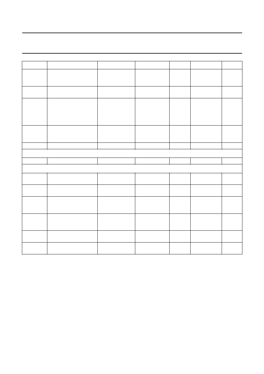
1997 May 30
29
Philips Semiconductors
Preliminary specification
Car radio Digital Signal Processor (CDSP)
SAA7707H
Notes
1. The values for the capitative load C
L
are given in pF.
2. R
L
is the AC impedance of the external circuitry at 1 kHz, connected to the audio outputs in the application. There is
also no DC current flowing through R
L
.
I
O(DAC; max)
maximum output current
from DACs
reference
resistance to
pin 14 = 18 k
490
570
650
µ
A
V
O(os)
DC offset voltage at DAC
output
with respect to
pin 20
-
5
-
mV
V
O(rms)
AC output voltage of
operational amplifier
outputs at maximum
signal pins 10, 12, 17
and 19 (RMS value)
R
L
>
5 k
;
R
fb
= 2.7 k
;
note 2
0.94
1.09
1.24
V
V
O(av)
average DC output
voltage at pins 10, 12,
17 and 19
R
L
> 5 k
;
R
fb
= 2.7 k
;
note 2
2.25
2.5
2.75
V
R
POM
pull-up resistor to pin 15
64
128
260
k
Crystal oscillator: T
amb
= 25
∞
C
V
DD(osc)
oscillator supply voltage
4.75
5.0
5.5
V
Current per supply pin or pin group: T
amb
= 25
∞
C; V
DD
= 5 V (typ.); 5.5 V (max.)
I
DDD1
digital supply current
DACs pin 7
-
20
50
µ
A
I
DDA
analog supply current
DAC pin 8
-
4
8
mA
I
DDO
supply current for
operational amplifiers
pin 15
no load
-
2
4
mA
I
DDD
supply current for digital
circuitry and periphery
pins 49, 52, 53 and 56
-
137.5
165
mA
I
DDX
supply current for crystal
circuit pin 65
-
1.5
3
mA
I
DDA1
supply current for ADCs
pin 69
-
15
20
mA
SYMBOL
PARAMETER
CONDITIONS
MIN.
TYP.
MAX.
UNIT
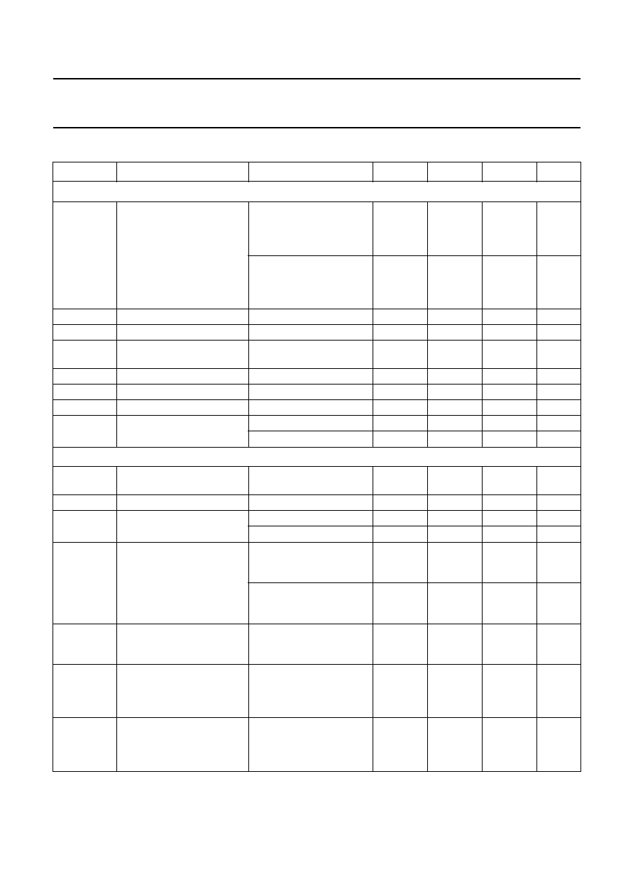
1997 May 30
30
Philips Semiconductors
Preliminary specification
Car radio Digital Signal Processor (CDSP)
SAA7707H
14 AC CHARACTERISTICS
SYMBOL
PARAMETER
CONDITIONS
MIN.
TYP.
MAX.
UNIT
Analog DC inputs (LEVEL-FM, AM): V
DDD
= V
DDA1
= 5 V; T
amb
= 25
∞
C
S/N
signal-to-noise ratio ADC
RMS value;
not weighted;
B = 0 to 29 kHz;
maximum input
48
54
-
dB
RMS value;
not weighted; audio
mode; B = 0 to 19 kHz;
maximum input
52
58
-
dB
R
i
input resistance
200
400
-
k
V
FS
full-scale input voltage
V
DDA1
= 4.75 to 5.5 V
1.05V
DDA1
1.1V
DDA1
1.15V
DDA1
V
V
I(os)
DC offset voltage at
minimum input voltage
with respect to V
DACNL
-
-
60
mV
V
iADR
input voltage level
R
ext
= 5 k
-
0.3
-
+7.5
V
decimation filter attenuation
20
-
-
dB/Dec
f
co
pass-band cut-off frequency at
-
3 dB
-
29
-
kHz
f
sr
sample rate after
decimation
radio mode
-
38
76
kHz
audio mode
-
38
76
kHz
Analog AC inputs: pins MPX, AM, TAPE and AUX
V
i(con, rms)
maximum conversion input
voltage level (RMS value)
THD
<
1%
1.1
-
-
V
R
i
input resistance
48
60
72
k
THD
total harmonic distortion
f
i
= 1 kHz; V
i
= 1 V (RMS)
-
-
71
-
61
dB
f
i
= 1 kHz; V
i
= 1 V (RMS)
-
0.03
0.09
%
S/N
ADC
signal-to-noise ratio for
ADC
not multiplexed;
B = 19 kHz;
V
i
= 1 V (RMS)
81
85
-
dB
multiplexed; unweighted;
B = 19 kHz;
V
i
= 1 V (RMS)
72
76
-
dB
S/N
AM
signal-to-noise ratio for AM
B = 5 kHz;
V
i
= 200 mV (RMS);
(M = 30%)
68
72
-
dB
S/N
FM(mon)
signal-to-noise-ratio for FM
mono
V
i
= 200 mV (RMS);
(
f = 22.5 kHz);
B = 19 kHz; unweighted;
(M = 30%)
69
72
-
dB
S/N
FM(st)
signal-to-noise-ratio for FM
stereo
V
i
= 200 mV (RMS);
(
f = 22.5 kHz);
B = 19 kHz; unweighted;
(M = 30%)
60
63
-
dB
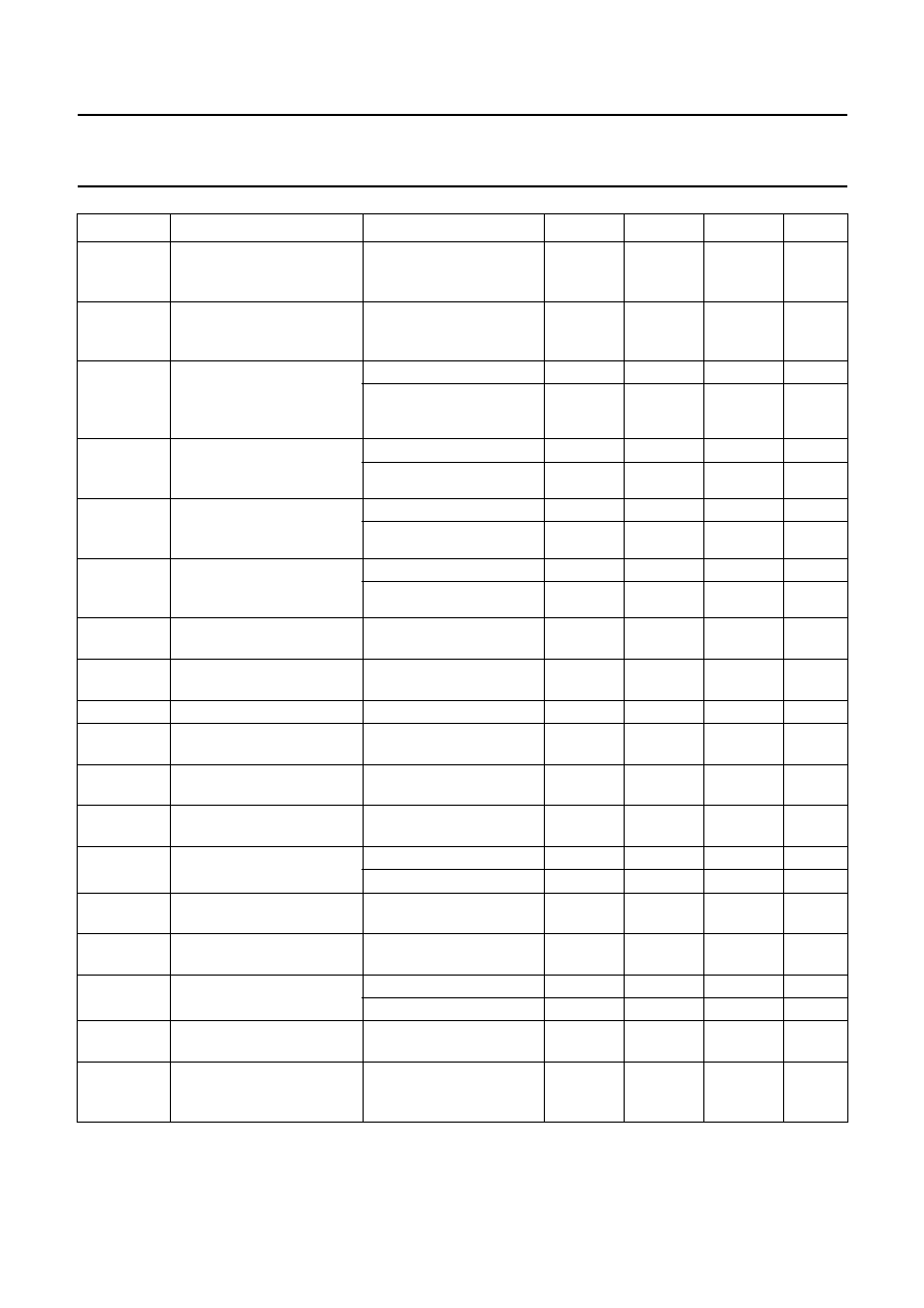
1997 May 30
31
Philips Semiconductors
Preliminary specification
Car radio Digital Signal Processor (CDSP)
SAA7707H
S/N
TAPE
signal-to-noise-ratio for
TAPE (+10 kHz RC)
B = 19 kHz;
V
i
= 1 V (RMS);
unweighted
70
74
-
dB
S/N
AUX
signal-to-noise-ratio for
AUX
B = 19 kHz;
V
i
= 1 V (RMS);
unweighted
72
76
-
dB
19
carrier and harmonic
suppression at the output
with and without modulation
(for 19 kHz including notch)
pilot signal f
i
= 19 kHz
-
81
-
dB
no modulation
-
98
-
dB
38
carrier and harmonic
suppression at the output
with and without modulation
subcarrier; f
i
= 38 kHz
-
83
-
dB
no modulation
-
91
-
dB
57
carrier and harmonic
suppression at the output
with and without modulation
subcarrier; f
i
= 57 kHz
-
83
-
dB
no modulation
-
96
-
dB
76
carrier and harmonic
suppression at the output
with and without modulation
subcarrier; f
i
= 76 kHz
-
84
-
dB
no modulation
-
94
-
dB
IM
10
intermodulation
f
mod
= 10 kHz;
f
spur
= 1 kHz; note 1
77
-
-
dB
IM
3
intermodulation
f
mod
= 13 kHz;
f
spur
= 1 kHz; note 1
76
-
-
dB
57(VF)
traffic radio suppression
f
i
= 57 kHz; note 2
-
110
-
dB
67
subsidiary communication
authority (SCA)
f
i
= 67 kHz; note 3
-
110
-
dB
114
adjacent channel
interference
f
i
= 114 kHz; note 4
-
110
-
dB
190
adjacent channel
interference
f
i
= 190 kHz; note 4
-
110
-
dB
V
pilot(rms)
pilot threshold voltage at
pin 42
stereo ON
-
35.6
-
mV
stereo OFF
-
35.5
-
mV
HYS
hysteresis level of pilot
voltage
-
0
-
dB
f
i
input frequency range MPX
-
3 dB; ADC via bitstream
test output
0
-
55
kHz
cs
FM stereo channel
separation
f
i
= 1 kHz
40
45
-
dB
f
i
= 10 kHz
25
30
-
dB
f
resFM
audio frequency response
FM
at
-
3 dB via DSP at DAC
output
16
-
-
kHz
|
G
v
|
channel unbalance
left/right TAPE, AUX, FM
and AM
-
-
0.5
dB
SYMBOL
PARAMETER
CONDITIONS
MIN.
TYP.
MAX.
UNIT

1997 May 30
32
Philips Semiconductors
Preliminary specification
Car radio Digital Signal Processor (CDSP)
SAA7707H
cs
channel separation TAPE
and AUX
f
i
= 1 kHz
40
45
-
dB
f
i
= 10 kHz
25
30
-
dB
f
i
= 1 kHz, software
compensated
-
50
-
dB
f
res
frequency response TAPE
and AUX
at
-
3 dB
18
-
-
kHz
ct
crosstalk between inputs
f
i
= 1 kHz
65
-
-
dB
f
i
= 15 kHz
50
-
-
dB
PSRR
power supply ripple
rejection for MPX and RDS
ADCs
output via I
2
S-bus;
ADC input shorted;
f
ripple
= 1 kHz;
V
ripple
= 100 mV (peak);
C
VrefMPX
= 22
µ
F;
C
VrefRDS
= 22
µ
F;
C
VDACPM
= 10
µ
F
35
45
-
dB
power supply ripple
rejection for ADC level
output via DAC;
ADC input shorted;
f
ripple
= 1 kHz;
V
ripple
= 100 mV (peak);
C
VrefRDS
= 22
µ
F
29
39
-
dB
Analog AC inputs: RDS
V
i(rms)
input voltage level
(RMS value)
THD
<
1%
1.1
-
-
V
R
i
input resistance RDS ADC
48
60
72
k
pilot
pilot attenuation RDS
50
-
-
dB
nearby selectivity RDS
neighbouring channel at
200 kHz distance
61
-
-
dB
mux
multiplex attenuation RDS
mono
70
-
-
dB
stereo
40
-
-
dB
f
osc
allowable frequency
deviation 57 kHz RDS
maximum crystal
deviation of 100 ppm
-
-
6
Hz
Analog outputs: V
DDD
= V
DDA
= V
DDO =
5 V; T
amb
= 25
∞
C
PSRR
power supply ripple
rejection DACs
input via I
2
S-bus;
f
ripple
= 1 kHz;
V
ripple
= 100 mV (peak);
C
Vref
= 22
µ
F
35
42
-
dB
V
o(DAC)
maximum deviation in
output level (plus or minus)
of the 4 DAC current
outputs
with respect to the
average of the 4 outputs;
tolerance R
o
< 0.1%;
full-scale output
-
-
0.38
dB
ct
crosstalk between all
outputs in the audio band
two outputs digital silence
other two maximum
volume; f
audio
= 10 kHz
-
-
-
60
dB
G
O
DC open loop gain of
operational amplifiers
-
85
-
dB
SYMBOL
PARAMETER
CONDITIONS
MIN.
TYP.
MAX.
UNIT

1997 May 30
33
Philips Semiconductors
Preliminary specification
Car radio Digital Signal Processor (CDSP)
SAA7707H
Z
o
AC output impedance of
operational amplifiers
R
L
>
5 k
;
note 5
-
1.5
-
f
ug
unity gain frequency
operational amplifiers
open loop
-
4.5
-
MHz
I
o(sc)
short-circuit current output
output short-circuited to
ground
-
10
25
mA
RES
DAC resolution
-
18
-
bits
(THD + N)/S DAC total harmonic
distortion plus
noise-to-signal ratio of
DAC and operational
amplifiers
f
i
= 1 kHz;
V
o
= 2.8 V (p-p)
(full-scale)
-
-
70
-
60
dB
f
i
= 1 kHz; at
-
60 dB;
A-weighted
-
-
38
-
28
dBA
DR
dynamic range
V
ref(o)
= 4.46 V (p-p);
f
i
= 1 kHz; at
-
60 dB;
A-weighted
92
102
-
dBA
DS
digital silence
V
ref(o)
= 4.46 V (p-p);
f
i
= 20 Hz to 17 kHz;
A-weighted
-
-
110
-
100
dBA
digital silence noise level at
output
RMS value; B = 20 kHz,
A-weighted
-
5
15
µ
V
IM
intermodulation
distortion/comparator
f
i
= 60 Hz and 7 kHz;
ratio 4 : 1
-
-
70
-
55
dB
f
s(max)
maximum sample
frequency
f
xtal
= 36.9 MHz
48
-
-
kHz
B
bandwidth of DAC
f
s
= f
s
-
3 dB
-
1
/
2
f
s
-
kHz
C
L
allowed load capacitance
on DAC voltage outputs
-
-
2.5
nF
R
L
allowed load resistor on
DAC voltage outputs
2
-
-
k
Crystal oscillator at: V
DDX
= 5 V; T
amb
= 25
∞
C
f
xtal
crystal frequency
-
36.860
-
MHz
f
spurious frequency
attenuation
20
-
-
dB
I
64
output current pin 64
-
-
1
mA
G
m
transconductance
at start-up
4
8
-
mS
V
xtal
voltage across crystal
-
500
-
mV
C
L
load capacitance
note 6
-
10
-
pF
R
xtal
allowed resistance loss of
crystal
C
p
= 5 pF; C
x1
= 10 pF;
C
x2
= 10 pF
-
20
100
SYMBOL
PARAMETER
CONDITIONS
MIN.
TYP.
MAX.
UNIT
1997 May 30
34
Philips Semiconductors
Preliminary specification
Car radio Digital Signal Processor (CDSP)
SAA7707H
Timing at: V
DDD
= V
DDA
= V
DDA1
= V
DDX
= 5 V; T
amb
= 25
∞
C
f
xtal
crystal frequency
-
36.860
-
MHz
f
xtal
/f
xtal
frequency adjustment
tolerance
-
30
-
+30
ppm
f
xtal
/
T
drift over temperature range
-
30
-
+30
ppm
f
i(max)
maximum input frequency
of I
2
C-bus clock
100
-
-
kHz
I
2
S-bus inputs and outputs (see Fig.18)
t
r
rise time
V
DDD
= 4.75 V;
T
amb
= 85
∞
C
-
-
4.75 +
0.28C
L
ns
V
DDD
= 5.5 V;
T
amb
=
-
40
∞
C
1.302 +
0.101C
L
-
-
ns
t
f
fall time
V
DDD
= 4.75 V;
T
amb
= 85
∞
C
-
-
6.44 +
0.36C
L
ns
V
DDD
= 5.5 V;
T
amb
=
-
40
∞
C
0.971 +
0.115C
L
-
-
ns
t
HC
clock output HIGH time
112
-
-
ns
t
LC
clock output LOW time
112
-
-
ns
t
dWS
Word Select delay time
0
-
-
ns
t
h
data hold time
0
-
-
ns
t
s
data set-up time
25
-
-
ns
t
d
data delay time
0
-
5
ns
t
a
data out access time
-
-
5 + 0.5C
L
ns
RDS; (see Figs.14 and 15)
f
clk
nominal clock frequency
RDS-clock
-
1187.5
-
Hz
t
s
clock set-up time
100
-
-
µ
s
T
cy
periodic time
-
842
-
µ
s
t
HC
clock HIGH time
220
-
640
µ
s
t
LC
clock LOW time
220
-
640
µ
s
t
h
data hold time
100
-
-
µ
s
t
w
wait time
1
-
-
µ
s
t
pb
periodic time
2
-
-
µ
s
t
HC
clock HIGH time
1
-
-
µ
s
t
LC
clock LOW time
1
-
-
µ
s
Other
f
EXCLK
input frequency on pin 40
-
-
22
MHz
SYMBOL
PARAMETER
CONDITIONS
MIN.
TYP.
MAX.
UNIT

1997 May 30
35
Philips Semiconductors
Preliminary specification
Car radio Digital Signal Processor (CDSP)
SAA7707H
Notes to the AC characteristics
1. Intermodulation suppression (BFC: Beat Frequency Components).
a)
2 = V
o(signal)
(at 1 kHz)/V
o(spurious)
(at 1 kHz); f
s
= (2
◊
10 kHz)
-
19 kHz.
b)
3 = V
o(signal)
(at 1 kHz)/V
o(spurious)
(at 1 kHz); f
s
= (3
◊
13 kHz)
-
38 kHz.
c) Measured with 91% mono signal; f
mod
= 10 or 13 kHz; 9% pilot signal.
2. Traffic radio (VF) suppression.
a)
57(VF) = V
o(signal)
(at 1 kHz)/V
o(spurious)
(at 1 kHz
±
23 Hz).
b) Measured with 91% stereo signal; f
mod
= 1 kHz; 9% pilot signal.
c) 5% traffic subcarrier (f = 57 kHz; f
mod
= 23 Hz AM, m = 0.6).
3. SCA (Subsidiary Communication Authorization).
a)
67 = V
o(signal)
(at 1 kHz)/V
o(spurious)
(at 9 kHz); f
s
= (2
◊
38 kHz)
-
67 kHz.
b) Measured with 81% mono signal; f
mod
= 1 kHz; 9% pilot signal.
c) 10% SCA subcarrier (f
s
= 67 kHz, unmodulated).
4. ACI (Adjacent Channel Interference).
a)
114 = V
o(signal)
(at 1 kHz)/V
o(spurious)
(at 4 kHz); f
s
= 110 kHz
-
(3
◊
38 kHz).
b)
190 = V
o(signal)
(at 1 kHz)/V
o(spurious)
(at 4 kHz); f
s
= 186 kHz
-
(5
◊
38 kHz).
c) Measured with 90% mono signal; f
mod
= 1 kHz; 9% pilot signal; 1% spurious signal (f
s
= 110 kHz or 186 kHz,
unmodulated).
5. R
L
is the AC impedance of the external circuitry at 1 kHz connected to the audio outputs in the application. There is
also no DC current flowing through R
L
.
6. The load capacitance is the sum of the series connection of C
◊
1 and C
◊
2 (see Fig.11) and the parasitic parallel
capacitor of the crystal C
p
.

1997 May 30
36
Philips Semiconductors
Preliminary specification
Car radio Digital Signal Processor (CDSP)
SAA7707H
15 I
2
C-BUS CONTROL AND COMMANDS
15.1
Characteristics of the I
2
C-bus
The I
2
C-bus is for 2-way, 2-line communication between
different ICs or modules. The two lines are a serial data
line (SDA) and a serial clock line (SCL). Both lines must be
connected to V
DDD
via a pull-up resistor when connected
to the output stages of a microcontroller. Data transfer can
only be initiated when the bus is not busy.
15.2
Bit transfer
One data bit is transferred during each clock pulse.
The data on the SDA line must remain stable during the
HIGH period of the clock pulse, as changes in the data line
at this time will be interpreted as control signals.
The maximum clock frequency is 100 kHz (see Fig.16).
15.3
START and STOP conditions
Both data and clock lines remain HIGH when the bus is not
busy. A HIGH-to-LOW transition of the data line, while the
clock is HIGH is defined as the START condition (S).
A LOW-to-HIGH transition of the data line while the clock
is HIGH is defined as the STOP condition (P) (see Fig.17).
15.4
Data transfer
A device generating a message is a `transmitter', a device
receiving a message is the `receiver'.
The device that controls the message is the `master' and
the devices that are controlled by the master are the
`slaves' (see Fig.18).
15.5
Acknowledge
The number of data bytes transferred between the START
and STOP conditions from transmitter to receiver is not
limited. Each byte of eight bits is followed by one
acknowledge bit. The acknowledge bit is a HIGH level put
on the bus by the transmitter, whereas the master
generates an extra acknowledge-related clock pulse.
A slave receiver that is addressed must generate an
acknowledge after the reception of each byte. Also, a
master must generate an acknowledge after the reception
of each byte that has been clocked out of the slave
transmitter.
The device that acknowledges has to pull down the SDA
line during the acknowledge clock pulse, so that the SDA
line is stable LOW during the HIGH period of the
acknowledge-related clock pulse. Set-up and hold times
must be taken into account. A master receiver must signal
an end-of-data to the transmitter by not generating an
acknowledge on the last byte that has been clocked out of
the slave. In this event, the transmitter must leave the data
line HIGH, to enable the master to generate a STOP
condition (see Fig.19).
15.6
I
2
C-bus format
15.6.1
A
DDRESSING
Before any data is transmitted on the I
2
C-bus, the device
that should respond is addressed first. The addressing is
always done with the first byte transmitted after the START
procedure.
15.6.2
S
LAVE ADDRESS
(A0
PIN
)
The CDSP acts as a slave receiver or slave transmitter.
Therefore, the clock signal SCL is only an input signal.
The data signal SDA is a bi-directional line. The CDSP
slave address is shown in Table 6.
Table 6
Slave address
The sub-address bit A0 corresponds to the hardware
address pin A0, which allows the device to have 1 of 2
different addresses. The A0 input is also used in test mode
as a serial input of the test control block.
15.6.3
CDSP
WRITE CYCLES
The I
2
C-bus configuration for a WRITE cycle is illustrated
in Fig.22. The WRITE cycle is used to write in the IAC
register, the input selector control register and to initialize
or update coefficient values in XRAM or YRAM. The data
is transferred from the I
2
C-bus register to the DSP register
once every DSP cycle.
The I
2
C-bus interface circuitry in the SAA7707H requires
that the LOW period of the SCL line following the
acknowledge bit is at least 1/f
s
(in seconds); where f
s
is the
audio sampling frequency (in Hertz). This requirement
must be met for a single write operation and an
auto-incremental operation, but only applies to the
acknowledge bit following each DATA-L
(see Figs 20 and 21).
The data length is 2 or 3 bytes, depending on the
accessed memory. If the Y-memory is addressed the data
length is 2 bytes, If the X-memory is addressed the length
is 3 bytes. The slave receiver detects the address and
adjusts the byte length accordingly.
MSB
LSB
0
0
1
1
1
0
A0
R/W
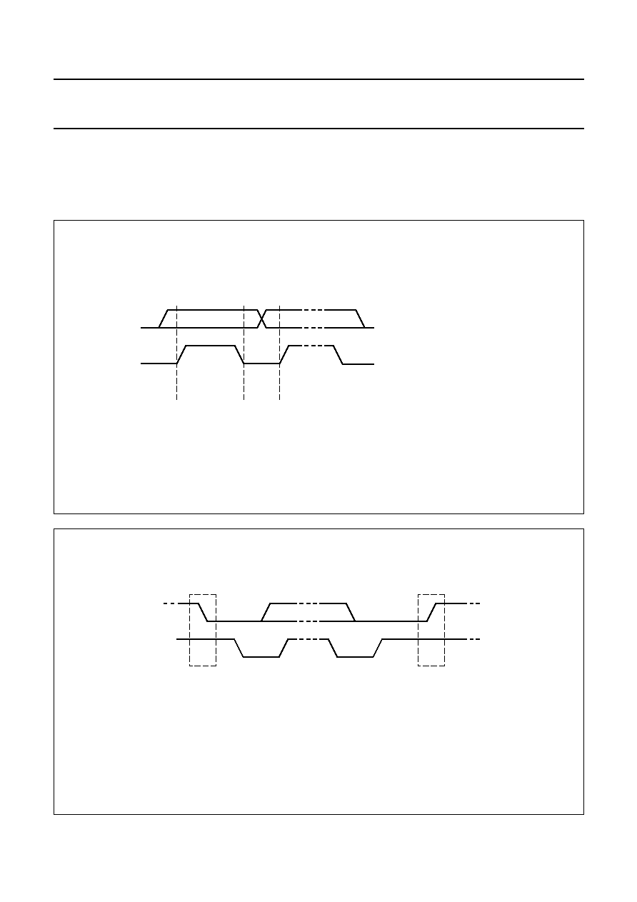
1997 May 30
37
Philips Semiconductors
Preliminary specification
Car radio Digital Signal Processor (CDSP)
SAA7707H
15.6.4
CDSP
READ CYCLES
The I
2
C-bus configuration for a READ cycle is illustrated in Fig.23. The READ cycle is used to read data values from
XRAM or YRAM. The data is transferred from the DSP register to the I
2
C-bus register at execution of the MPI instruction
in the DSP program. Therefore, an MPI instruction should be added at least once every DSP cycle.
Fig.16 Bit transfer on the I
2
C-bus.
th
MBC621
data line
stable;
data valid
change
of data
allowed
SDA
SCL
Fig.17 START and STOP conditions.
handbook, full pagewidth
MBC622
SDA
SCL
P
STOP condition
SDA
SCL
S
START condition
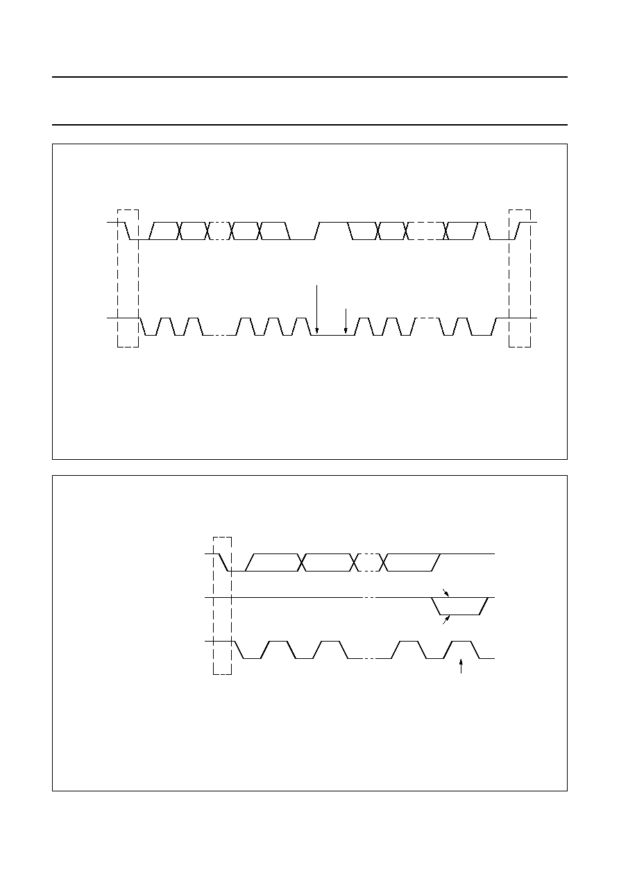
1997 May 30
38
Philips Semiconductors
Preliminary specification
Car radio Digital Signal Processor (CDSP)
SAA7707H
Fig.18 Data transfer on the I
2
C-bus.
handbook, full pagewidth
MBH177
P
S
SDA
SCL
START
CONDITION
STOP
CONDITION
1
2
3 - 8
9
ACK
9
ACK
7
8
1
2
MSB
acknowledgement
signal from receiver
byte complete;
interrupt within receiver
clock line held low while
interrupts are serviced
acknowledgement
signal from receiver
Fig.19 Acknowledge on the I
2
C-bus.
MBH178
S
START
CONDITION
9
8
2
1
clock pulse for
acknowledgement
not acknowledge
acknowledge
DATA OUTPUT
BY TRANSMITTER
DATA OUTPUT
BY RECEIVER
SCL FROM
MASTER
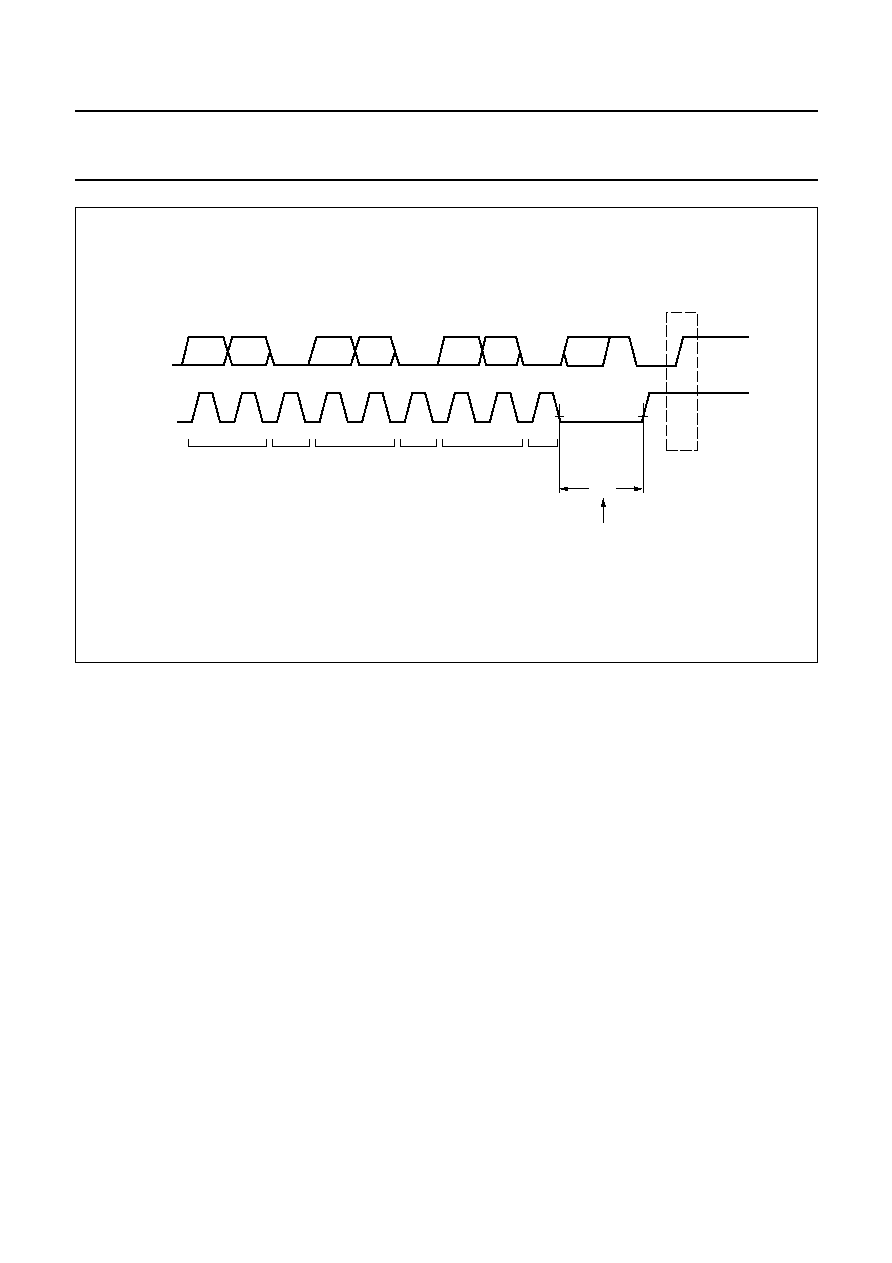
1997 May 30
39
Philips Semiconductors
Preliminary specification
Car radio Digital Signal Processor (CDSP)
SAA7707H
Fig.20 Minimum required SCL LOW period; single write.
handbook, full pagewidth
MGK426
1/fs
DATA-M
DATA-L
DATA-H
ACK
SDA
SCL
ACK
ACK
minimum required LOW period
STOP
condition
P
1-7
8
9
1-7
8
9
1-7
8
9
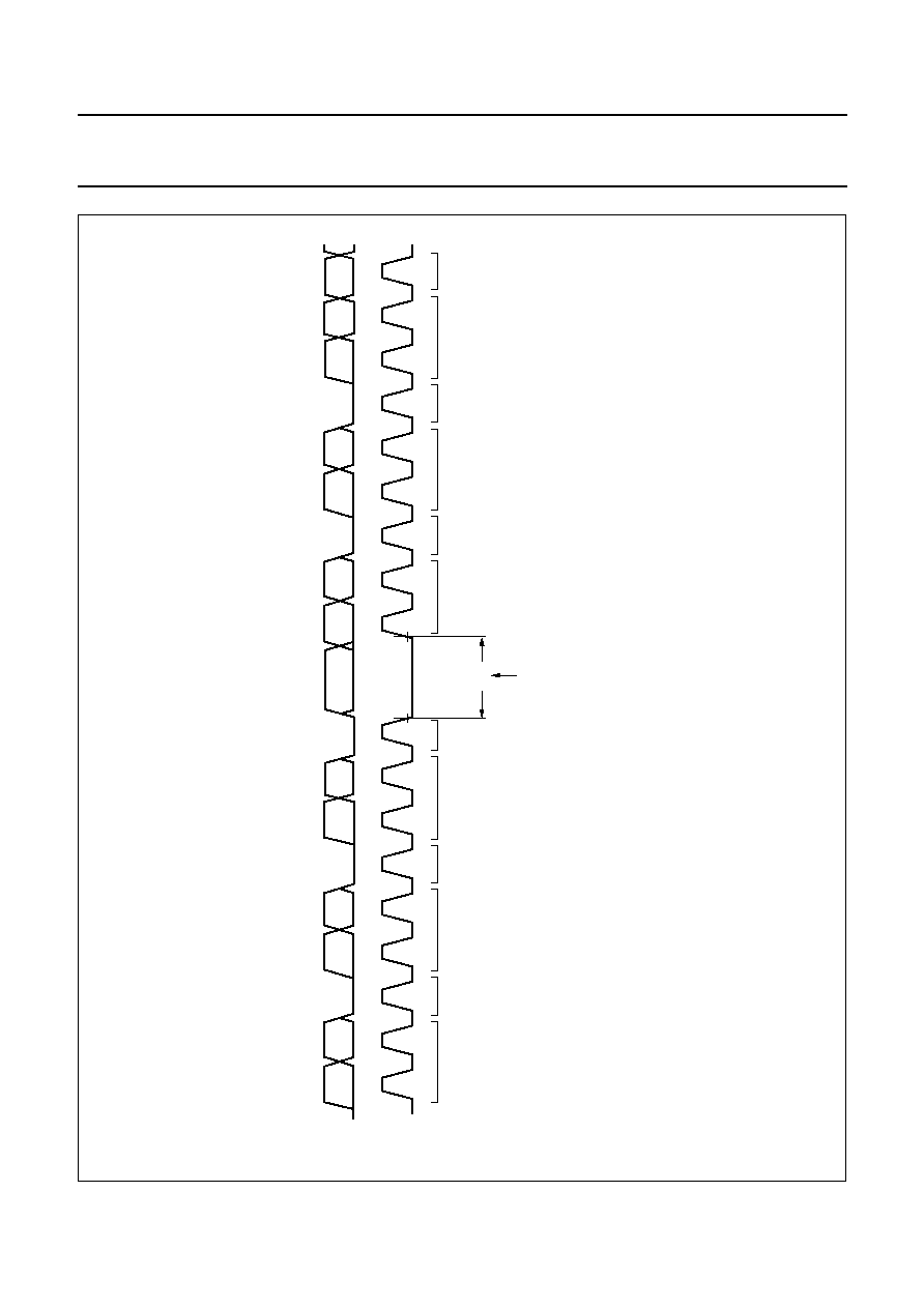
1997
May
30
40
Philips Semiconductors
Preliminary specification
Car radio Digital Signal Processor (CDSP)
SAA7707H
This text is here in white to force landscape pages to be rotated correctly when browsing through the pdf in the Acrobat reader.This text is here in
_
white to force landscape pages to be rotated correctly when browsing through the pdf in the Acrobat reader.This text is here inThis text is here in
white to force landscape pages to be rotated correctly when browsing through the pdf in the Acrobat reader. white to force landscape pages to be ...
Fig.21 Minimum required SCL LOW period; auto-incremental write.
k
, full pagewidth
1/fs
DATA-M
DATA-L
DATA-H
ACK
SDA
SCL
ACK
ACK
minimum required LOW period
1-7
8
9
1-7
8
9
1-7
8
9
MGK427
DATA-M
DATA-L
DATA-H
ACK
ACK
ACK
1-7
8
9
1-7
8
9
1-7
8
9

1997
May
30
41
Philips Semiconductors
Preliminary specification
Car radio Digital Signal Processor (CDSP)
SAA7707H
This text is here in white to force landscape pages to be rotated correctly when browsing through the pdf in the Acrobat reader.This text is here in
_
white to force landscape pages to be rotated correctly when browsing through the pdf in the Acrobat reader.This text is here inThis text is here in
white to force landscape pages to be rotated correctly when browsing through the pdf in the Acrobat reader. white to force landscape pages to be ...
16 SOFTWARE DESCRIPTION
A detailed description of the software feature, complete with operating instructions, is provided in the application manual.
17 APPLICATION INFORMATION
The application diagram illustrated in Figs. 24 and 25 must be considered as one of the examples of a (limited) application of the SAA7707H.
For example, in the application shown, the I
2
S-bus inputs of the DCC and CD are not used.
0 1 1 1 0 0 0
A
C
K
A
C
K
A
C
K
A
C
K
A
C
K
address
S
0
ADDR H
ADDR L
DATA H
DATA M
R/W
MGD568
auto increment if repeated n-groups of 3 (2) bytes
P
A
C
K
DATA L
Fig.22 Master transmitter writes to CDSP registers.
0 1 1 1 0 0 0
A
C
K
A
C
K
A
C
K
A
C
K
A
C
K
address
S
0
0 1 1
1
1 0 0
S
0
ADDR H
ADDR L
DATA H
R/W
MGA808 - 1
auto increment if repeated n-groups of 3 (2) bytes
P
A
C
K
A
C
K
DATA M
DATA L
R/W
Fig.23 Master transmitter reads from CDSP registers.
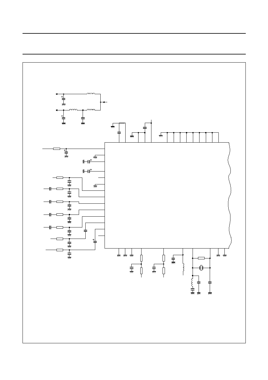
1997 May 30
42
Philips Semiconductors
Preliminary specification
Car radio Digital Signal Processor (CDSP)
SAA7707H
Fig.24 Application diagram (continued in Fig.25).
handbook, full pagewidth
MBH179
77
70
62
79
32
FMRDS
FMMPX
AMAF
AUXR
TAPER
AUXL
AUXR
FM
AM
MPXRDS
VDACNM
VDACPM
VrefMPX
VrefRDS
RTCB
80
C5
78
4
33
SHTCB
30
TSCAN
66
V
SSX
23
CDCLK
60
RDSCLK
3
72
71
22
µ
F
C6
C7
22
µ
F
1 nF
470 nF
C8
330
pF
R2
4.7 k
75
220
pF
R7
3.3 k
R3
C14
4.7 k
470 nF
C9
330
pF
R4
C15
4.7 k
74
470 nF
C10
3.3
nF
R5
C16
4.7 k
72
470 nF
C11
C22
100
nF
C24
C13
C18
3.3
nF
220
nF
76
150
pF
C12
330
pF
R7
3.3 k
C19
1
µ
F
R6
C17
4.7 k
LEVEL (AM, FM)
C4
10
µ
F
R1
1 k
+
5 V
CDIN-R
CDIN-L
CASS-R
CASS-L
RADIO-F (AM)
MPX (FM)
R9
100
R10
100
61
RDSDAT
65
64
63
L4
L5
4.7
µ
H
C25
4.7 nF
C26
10 pF
C27
10 pF
V
DDX
XTALO
XTALI
220
pF
C23
R11
100
R12
100
100 k
RDSCLK
RDSDAT
BLM21A10
+5 V (e.g.)
X1
R13
36.86 MHz
C3
100 nF
C2
100
µ
F
C1
4.7
µ
F
10
µ
H
220
µ
H
L3
BLM21A10
L2
L1
5
22
V
SSD1
V
SSD2
50
67
68
69
51
V
SSD3
V
SSG
V
SSA1
V
DDA1
V
SSD4
54
55
V
SSD5
V
SSD6
34
41
V
SSD7
V
SSD8
29
V
SSD9
C21
100 nF
2
1
CINT
V
DACNL
C20
1 nF
+
5 V
+
5 V
+
5 V
+
5 V
SAA7707H
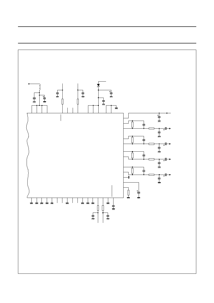
1997 May 30
43
Philips Semiconductors
Preliminary specification
Car radio Digital Signal Processor (CDSP)
SAA7707H
book, full pagewidth
MBH180
24
DCWS
25
CDDAT
48
DCCDAT
47
DCCWS
46
DCCCLK
28
27
37
59
TEST2
57
TEST1
38
39
C28
100 pF
C29
100 pF
R14
220
R15
220
SCL SDA
58
V
SSD10
35
EXDAT
EXDAT2
EXDAT1
36
EXSCL
EXWS
31
A0
C30
220 nF
R22
18 k
C42
22
µ
F
C32
100
µ
F
L6
BLM32A07
C33
100 pF
C31
100 nF
26
DSPRESET
SCL
SDA
13
20
40
R20
2.7 K
C40
2.2 nF
C48 2.2
µ
F
C47
10 nF
Iref(int)
Vref
EXCLK
11
12
REAR-LEFT
RIOL
RVOL
RIOR
RVOR
17
FVOR
16
FIOR
100
R25
R19
2.7 K
C39
2.2 nF
C46 2.2
µ
F
C45
10 nF
C43
10 nF
FRONT-RIGHT
100
R24
19
FVOL
18
FIOL
C37
4.7
µ
F
21
POM
R18
2.7 K
C38
2.2 nF
C44 2.2
µ
F
FRONT-LEFT
MICROCONTROLLER
100
R23
R21
2.7 K
C41
2.2 nF
C50 2.2
µ
F
C49
10 nF
9
10
REAR-RIGHT
100
R26
56
V
DDD2
49
V
DDD3
52
V
DDD4
53
V
DDD5
7
V
DDD1
8
V
DDA
14
V
SSO
6
V
SSA
15
V
DDO
45
44
DEEM
MUTE
42
43
STEREO
MSS/P
C34
100 pF
C35
100 nF
D1
BAT54
C36
22
µ
F
+
5 V
R17
220
R16
220
+
5 V
RDSMUTE
PAUSE
SAA7707H
Fig.25 Application diagram (continued from Fig.24).

1997 May 30
44
Philips Semiconductors
Preliminary specification
Car radio Digital Signal Processor (CDSP)
SAA7707H
18 PACKAGE OUTLINE
UNIT
A
1
A
2
A
3
b
p
c
E
(1)
e
H
E
L
L
p
Z
y
w
v
REFERENCES
OUTLINE
VERSION
EUROPEAN
PROJECTION
ISSUE DATE
IEC
JEDEC
EIAJ
mm
0.25
0.05
2.90
2.65
0.25
0.45
0.30
0.25
0.14
14.1
13.9
0.8
1.95
18.2
17.6
1.2
0.8
7
0
o
o
0.2
0.2
0.1
DIMENSIONS (mm are the original dimensions)
Note
1. Plastic or metal protrusions of 0.25 mm maximum per side are not included.
1.0
0.6
SOT318-2
D
(1)
(1)
(1)
20.1
19.9
H
D
24.2
23.6
E
Z
1.0
0.6
D
b
p
e
E
A
1
A
L
p
detail X
L
(A )
3
B
24
c
b
p
E
H
A
2
D
Z D
A
Z E
e
v
M
A
1
80
65
64
41
40
25
pin 1 index
X
y
D
H
v
M
B
w
M
w
M
95-02-04
97-08-01
0
5
10 mm
scale
QFP80: plastic quad flat package; 80 leads (lead length 1.95 mm); body 14 x 20 x 2.8 mm
SOT318-2
A
max.
3.2

1997 May 30
45
Philips Semiconductors
Preliminary specification
Car radio Digital Signal Processor (CDSP)
SAA7707H
19 SOLDERING
19.1
Introduction
There is no soldering method that is ideal for all IC
packages. Wave soldering is often preferred when
through-hole and surface mounted components are mixed
on one printed-circuit board. However, wave soldering is
not always suitable for surface mounted ICs, or for
printed-circuits with high population densities. In these
situations reflow soldering is often used.
This text gives a very brief insight to a complex technology.
A more in-depth account of soldering ICs can be found in
our
"IC Package Databook" (order code 9398 652 90011).
19.2
Reflow soldering
Reflow soldering techniques are suitable for all QFP
packages.
The choice of heating method may be influenced by larger
plastic QFP packages (44 leads, or more). If infrared or
vapour phase heating is used and the large packages are
not absolutely dry (less than 0.1% moisture content by
weight), vaporization of the small amount of moisture in
them can cause cracking of the plastic body. For more
information, refer to the Drypack chapter in our
"Quality
Reference Handbook" (order code 9397 750 00192).
Reflow soldering requires solder paste (a suspension of
fine solder particles, flux and binding agent) to be applied
to the printed-circuit board by screen printing, stencilling or
pressure-syringe dispensing before package placement.
Several techniques exist for reflowing; for example,
thermal conduction by heated belt. Dwell times vary
between 50 and 300 seconds depending on heating
method. Typical reflow temperatures range from
215 to 250
∞
C.
Preheating is necessary to dry the paste and evaporate
the binding agent. Preheating duration: 45 minutes at
45
∞
C.
19.3
Wave soldering
Wave soldering is not recommended for QFP packages.
This is because of the likelihood of solder bridging due to
closely-spaced leads and the possibility of incomplete
solder penetration in multi-lead devices.
If wave soldering cannot be avoided, the following
conditions must be observed:
∑
A double-wave (a turbulent wave with high upward
pressure followed by a smooth laminar wave)
soldering technique should be used.
∑
The footprint must be at an angle of 45
∞
to the board
direction and must incorporate solder thieves
downstream and at the side corners.
Even with these conditions, do not consider wave
soldering the following packages: QFP52 (SOT379-1),
QFP100 (SOT317-1), QFP100 (SOT317-2),
QFP100 (SOT382-1) or QFP160 (SOT322-1).
During placement and before soldering, the package must
be fixed with a droplet of adhesive. The adhesive can be
applied by screen printing, pin transfer or syringe
dispensing. The package can be soldered after the
adhesive is cured.
Maximum permissible solder temperature is 260
∞
C, and
maximum duration of package immersion in solder is
10 seconds, if cooled to less than 150
∞
C within
6 seconds. Typical dwell time is 4 seconds at 250
∞
C.
A mildly-activated flux will eliminate the need for removal
of corrosive residues in most applications.
19.4
Repairing soldered joints
Fix the component by first soldering two diagonally-
opposite end leads. Use only a low voltage soldering iron
(less than 24 V) applied to the flat part of the lead. Contact
time must be limited to 10 seconds at up to 300
∞
C. When
using a dedicated tool, all other leads can be soldered in
one operation within 2 to 5 seconds between
270 and 320
∞
C.
1997 May 30
46
Philips Semiconductors
Preliminary specification
Car radio Digital Signal Processor (CDSP)
SAA7707H
20 DEFINITIONS
21 LIFE SUPPORT APPLICATIONS
These products are not designed for use in life support appliances, devices, or systems where malfunction of these
products can reasonably be expected to result in personal injury. Philips customers using or selling these products for
use in such applications do so at their own risk and agree to fully indemnify Philips for any damages resulting from such
improper use or sale.
22 PURCHASE OF PHILIPS I
2
C COMPONENTS
Data sheet status
Objective specification
This data sheet contains target or goal specifications for product development.
Preliminary specification
This data sheet contains preliminary data; supplementary data may be published later.
Product specification
This data sheet contains final product specifications.
Limiting values
Limiting values given are in accordance with the Absolute Maximum Rating System (IEC 134). Stress above one or
more of the limiting values may cause permanent damage to the device. These are stress ratings only and operation
of the device at these or at any other conditions above those given in the Characteristics sections of the specification
is not implied. Exposure to limiting values for extended periods may affect device reliability.
Application information
Where application information is given, it is advisory and does not form part of the specification.
Purchase of Philips I
2
C components conveys a license under the Philips' I
2
C patent to use the
components in the I
2
C system provided the system conforms to the I
2
C specification defined by
Philips. This specification can be ordered using the code 9398 393 40011.

1997 May 30
47
Philips Semiconductors
Preliminary specification
Car radio Digital Signal Processor (CDSP)
SAA7707H
NOTES

Internet: http://www.semiconductors.philips.com
Philips Semiconductors ≠ a worldwide company
© Philips Electronics N.V. 1997
SCA54
All rights are reserved. Reproduction in whole or in part is prohibited without the prior written consent of the copyright owner.
The information presented in this document does not form part of any quotation or contract, is believed to be accurate and reliable and may be changed
without notice. No liability will be accepted by the publisher for any consequence of its use. Publication thereof does not convey nor imply any license
under patent- or other industrial or intellectual property rights.
Netherlands: Postbus 90050, 5600 PB EINDHOVEN, Bldg. VB,
Tel. +31 40 27 82785, Fax. +31 40 27 88399
New Zealand: 2 Wagener Place, C.P.O. Box 1041, AUCKLAND,
Tel. +64 9 849 4160, Fax. +64 9 849 7811
Norway: Box 1, Manglerud 0612, OSLO,
Tel. +47 22 74 8000, Fax. +47 22 74 8341
Philippines: Philips Semiconductors Philippines Inc.,
106 Valero St. Salcedo Village, P.O. Box 2108 MCC, MAKATI,
Metro MANILA, Tel. +63 2 816 6380, Fax. +63 2 817 3474
Poland: Ul. Lukiska 10, PL 04-123 WARSZAWA,
Tel. +48 22 612 2831, Fax. +48 22 612 2327
Portugal: see Spain
Romania: see Italy
Russia: Philips Russia, Ul. Usatcheva 35A, 119048 MOSCOW,
Tel. +7 095 755 6918, Fax. +7 095 755 6919
Singapore: Lorong 1, Toa Payoh, SINGAPORE 1231,
Tel. +65 350 2538, Fax. +65 251 6500
Slovakia: see Austria
Slovenia: see Italy
South Africa: S.A. PHILIPS Pty Ltd., 195-215 Main Road Martindale,
2092 JOHANNESBURG, P.O. Box 7430 Johannesburg 2000,
Tel. +27 11 470 5911, Fax. +27 11 470 5494
South America: Rua do Rocio 220, 5th floor, Suite 51,
04552-903 S„o Paulo, S√O PAULO - SP, Brazil,
Tel. +55 11 821 2333, Fax. +55 11 829 1849
Spain: Balmes 22, 08007 BARCELONA,
Tel. +34 3 301 6312, Fax. +34 3 301 4107
Sweden: Kottbygatan 7, Akalla, S-16485 STOCKHOLM,
Tel. +46 8 632 2000, Fax. +46 8 632 2745
Switzerland: Allmendstrasse 140, CH-8027 ZÐRICH,
Tel. +41 1 488 2686, Fax. +41 1 481 7730
Taiwan: Philips Semiconductors, 6F, No. 96, Chien Kuo N. Rd., Sec. 1,
TAIPEI, Taiwan Tel. +886 2 2134 2865, Fax. +886 2 2134 2874
Thailand: PHILIPS ELECTRONICS (THAILAND) Ltd.,
209/2 Sanpavuth-Bangna Road Prakanong, BANGKOK 10260,
Tel. +66 2 745 4090, Fax. +66 2 398 0793
Turkey: Talatpasa Cad. No. 5, 80640 GÐLTEPE/ISTANBUL,
Tel. +90 212 279 2770, Fax. +90 212 282 6707
Ukraine: PHILIPS UKRAINE, 4 Patrice Lumumba str., Building B, Floor 7,
252042 KIEV, Tel. +380 44 264 2776, Fax. +380 44 268 0461
United Kingdom: Philips Semiconductors Ltd., 276 Bath Road, Hayes,
MIDDLESEX UB3 5BX, Tel. +44 181 730 5000, Fax. +44 181 754 8421
United States: 811 East Arques Avenue, SUNNYVALE, CA 94088-3409,
Tel. +1 800 234 7381
Uruguay: see South America
Vietnam: see Singapore
Yugoslavia: PHILIPS, Trg N. Pasica 5/v, 11000 BEOGRAD,
Tel. +381 11 625 344, Fax.+381 11 635 777
For all other countries apply to: Philips Semiconductors, Marketing & Sales Communications,
Building BE-p, P.O. Box 218, 5600 MD EINDHOVEN, The Netherlands, Fax. +31 40 27 24825
Argentina: see South America
Australia: 34 Waterloo Road, NORTH RYDE, NSW 2113,
Tel. +61 2 9805 4455, Fax. +61 2 9805 4466
Austria: Computerstr. 6, A-1101 WIEN, P.O. Box 213,
Tel. +43 1 60 101, Fax. +43 1 60 101 1210
Belarus: Hotel Minsk Business Center, Bld. 3, r. 1211, Volodarski Str. 6,
220050 MINSK, Tel. +375 172 200 733, Fax. +375 172 200 773
Belgium: see The Netherlands
Brazil: see South America
Bulgaria: Philips Bulgaria Ltd., Energoproject, 15th floor,
51 James Bourchier Blvd., 1407 SOFIA,
Tel. +359 2 689 211, Fax. +359 2 689 102
Canada: PHILIPS SEMICONDUCTORS/COMPONENTS,
Tel. +1 800 234 7381
China/Hong Kong: 501 Hong Kong Industrial Technology Centre,
72 Tat Chee Avenue, Kowloon Tong, HONG KONG,
Tel. +852 2319 7888, Fax. +852 2319 7700
Colombia: see South America
Czech Republic: see Austria
Denmark: Prags Boulevard 80, PB 1919, DK-2300 COPENHAGEN S,
Tel. +45 32 88 2636, Fax. +45 31 57 0044
Finland: Sinikalliontie 3, FIN-02630 ESPOO,
Tel. +358 9 615800, Fax. +358 9 61580920
France: 4 Rue du Port-aux-Vins, BP317, 92156 SURESNES Cedex,
Tel. +33 1 40 99 6161, Fax. +33 1 40 99 6427
Germany: Hammerbrookstraþe 69, D-20097 HAMBURG,
Tel. +49 40 23 53 60, Fax. +49 40 23 536 300
Greece: No. 15, 25th March Street, GR 17778 TAVROS/ATHENS,
Tel. +30 1 4894 339/239, Fax. +30 1 4814 240
Hungary: see Austria
India: Philips INDIA Ltd, Shivsagar Estate, A Block, Dr. Annie Besant Rd.
Worli, MUMBAI 400 018, Tel. +91 22 4938 541, Fax. +91 22 4938 722
Indonesia: see Singapore
Ireland: Newstead, Clonskeagh, DUBLIN 14,
Tel. +353 1 7640 000, Fax. +353 1 7640 200
Israel: RAPAC Electronics, 7 Kehilat Saloniki St, PO Box 18053,
TEL AVIV 61180, Tel. +972 3 645 0444, Fax. +972 3 649 1007
Italy: PHILIPS SEMICONDUCTORS, Piazza IV Novembre 3,
20124 MILANO, Tel. +39 2 6752 2531, Fax. +39 2 6752 2557
Japan: Philips Bldg 13-37, Kohnan 2-chome, Minato-ku, TOKYO 108,
Tel. +81 3 3740 5130, Fax. +81 3 3740 5077
Korea: Philips House, 260-199 Itaewon-dong, Yongsan-ku, SEOUL,
Tel. +82 2 709 1412, Fax. +82 2 709 1415
Malaysia: No. 76 Jalan Universiti, 46200 PETALING JAYA, SELANGOR,
Tel. +60 3 750 5214, Fax. +60 3 757 4880
Mexico: 5900 Gateway East, Suite 200, EL PASO, TEXAS 79905,
Tel. +9-5 800 234 7381
Middle East: see Italy
Printed in The Netherlands
547027/1200/02/pp48
Date of release: 1997 May 30
Document order number:
9397 750 02261