 | –≠–ª–µ–∫—Ç—Ä–æ–Ω–Ω—ã–π –∫–æ–º–ø–æ–Ω–µ–Ω—Ç: SAA7712H | –°–∫–∞—á–∞—Ç—å:  PDF PDF  ZIP ZIP |
DATA SHEET
Preliminary specification
File under Integrated Circuits, IC02
1999 Aug 05
INTEGRATED CIRCUITS
SAA7712H
Sound effects DSP

1999 Aug 05
2
Philips Semiconductors
Preliminary specification
Sound effects DSP
SAA7712H
CONTENTS
1
FEATURES
1.1
Hardware features
1.2
Software features
2
APPLICATIONS
3
GENERAL DESCRIPTION
4
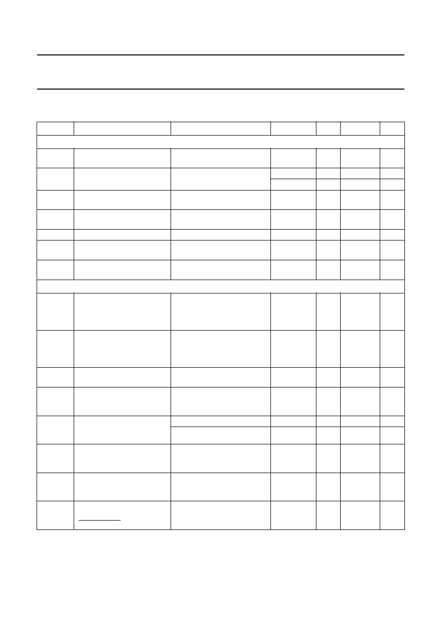
QUICK REFERENCE DATA
5
ORDERING INFORMATION
6
BLOCK DIAGRAM
7
PINNING INFORMATION
8
FUNCTIONAL DESCRIPTION
8.1
Analog outputs
8.1.1
Analog output circuit
8.1.2
DAC frequency
8.1.3
DACs
8.1.4
Upsample filter
8.1.5
Performance
8.1.6
Power-On Mute (POM)
8.1.7
Power-off plop suppression
8.1.8
Pin VREFDA
8.1.9
Internal DAC current reference
8.1.10
Supply of the analog outputs
8.2
I
2
S-bus inputs and outputs
8.2.1
Digital data stream formats
8.2.2
Slave I
2
S-bus inputs
8.2.3
Master I
2
S-bus inputs and outputs
8.3
Equalizer accelerator
8.3.1
Introduction
8.3.2
Configuration of equalizer sections
8.3.3
Overflow detection
8.4
Clock circuit and oscillator
8.4.1
General description
8.4.2
Supply of the crystal oscillator
8.5
Programmable phase-locked loop circuit
8.6
I
2
C-bus control
8.6.1
Introduction
8.6.2
Characteristics of the I
2
C-bus
8.6.3
Bit transfer
8.6.4
Start and stop conditions
8.6.5
Data transfer
8.6.6
Acknowledge
8.6.7
State of the I
2
C-bus interface during and after
Power-on reset
8.7
External control pins
8.8
Reset pin
8.9
Power supply connection and EMC
8.10
Test mode connections
9
I
2
C-BUS FORMAT
9.1
Addressing
9.2
Slave address (pin A0)
9.3
Write cycles
9.4
Read cycles
9.5
I
2
C-bus memory map summary
9.6
I
2
C-bus memory map details
10
LIMITING VALUES
11
THERMAL CHARACTERISTICS
12
DC CHARACTERISTICS
13
ANALOG OUTPUTS CHARACTERISTICS
14
OSCILLATOR CHARACTERISTICS
15
I
2
S-BUS TIMING CHARACTERISTICS
16
I
2
C-BUS TIMING CHARACTERISTICS
17
APPLICATION INFORMATION
18
PACKAGE OUTLINE
19
SOLDERING
19.1
Introduction to soldering surface mount
packages
19.2
Reflow soldering
19.3
Wave soldering
19.4
Manual soldering
19.5
Suitability of surface mount IC packages for
wave and reflow soldering methods
20
DEFINITIONS
21
LIFE SUPPORT APPLICATIONS
22
PURCHASE OF PHILIPS I
2
C COMPONENTS

1999 Aug 05
3
Philips Semiconductors
Preliminary specification
Sound effects DSP
SAA7712H
1
FEATURES
1.1
Hardware features
∑
Digital Signal Processor (DSP) core:
≠ 18 bits data width, 12 bits coefficient width
≠ Separate X, Y and P memories (both 384 bytes word
XRAM and YRAM, 3 kbytes word PROM)
≠ 1 kbytes delay line memory suited for Dolby Pro
Logic Surround.
∑
Inputs:
≠ 2 slave 18-bit digital stereo inputs: I
2
S-bus and
LSB-justified serial formats
≠ 2 master 18-bit digital stereo inputs: I
2
S-bus and
LSB-justified serial formats.
∑
Outputs:
≠ 4 DACs with 4-times oversampling and noise
shaping, fed to 4 output pins and configurable from
the DSP program, as left, right, front and surround
channels of a Dolby Pro Logic Surround system
≠ 2 master 18-bit digital stereo outputs: I
2
S-bus and
LSB-justified serial formats.
∑
4-channel 5-band or 2-channel 10-band
I
2
C-bus controlled parametric equalizer
∑
I
2
C-bus microcontroller interface for:
≠ Access to full X and Y memory space
≠ Control of hardware settings: selectors,
programmable clock generations, etc.
∑
Controllable Phase-Locked Loop (PLL) to generate the
high frequency DSP clock from common fundamental
oscillator crystal
∑
3.3 V process with 3.3 or 5 V digital periphery:
≠ 3.3 or 5 V I
2
S-bus and I
2
C-bus microcontroller
interfacing.
∑
Operating temperature range from 0 to 70
∞
C.
1.2
Software features
∑
Dolby Pro Logic Surround/Dolby 3 stereo:
Trademark of Dolby Laboratories Licensing Corporation
∑
Noise generation: A pink noise generator is included
for installation of the Dolby Pro Logic/Dolby 3 stereo
mode
∑
Hall/Matrix Surround: When no Dolby Pro Logic
Surround source material is available then this mode
can be used to produce a signal in the surround channel
∑
Incredible Surround (222-IS): This algorithm expands
the stereo width (stereo expander). This is intended to
be used when the 2 speakers are placed close together
(TV set and Midi set).
∑
Robust Incredible Surround (222-RIS): Same as
incredible surround only an alternative algorithm
∑
3D Surround (422) or Incredible Virtual Surround:
Dolby Pro Logic Surround reproduced by 2 speakers
(L and R)
∑
IS-3D Surround (422-IS): Same as 3D Surround (422)
only with extra stereo width expander on left and right
∑
RIS-3D Surround (422-RIS): Same as IS-3D Surround
(422) with alternative algorithm
∑
3D Surround (423) or Incredible Virtual Surround:
Dolby Pro Logic Surround reproduced by 3 speakers
(L, C and R)
∑
IS-3D Surround (423-IS): Same as 3D Surround (423)
only with extra stereo width expander on left and right
∑
RIS-3D Surround (423-RIS): Same as IS-3D Surround
(423-IS) with alternative algorithm

1999 Aug 05
4
Philips Semiconductors
Preliminary specification
Sound effects DSP
SAA7712H
∑
Voice cancelling (karaoke): Rejects voice out of
source material, mainly intended to be used with
karaoke. Several karaoke modes available in stereo
mode and in Dolby Pro Logic mode, such as (auto) voice
cancel, (auto) centre voice cancel, (auto) multi left and
(auto) multi right.
∑
Microphone mix modes (karaoke): Mono microphone
mixed to left, right and centre channel
∑
Spectrum analysis: 3-band spectrum analyser is
provided
∑
Dolby B: Both a Dolby B encoder as well as a Dolby B
decoder is implemented
∑
2 Room solution: In all modes not requiring more than
2 output channels (stereo and karaoke incredible
surround) it is also possible to feed the source signal to
the other 2 output channels (with same processed or
not processed signal)
∑
Dynamic Bass Enhancement (DBE): Dynamic bass
enhancement generates a sub-woofer channel, which is
either a separate output or is added to the front channels
∑
Volume processing: Independent volume processing
of all 4 output channels
∑
AC-3/MPEG-2: Inputs available intended to be used
with an AC-3/MPEG-2 co-processor. In this mode the
SAA7712H can be used as post-processor.
∑
Output redirection: Several output configurations are
possible (normal 4 channel, special 4 + 2 channel,
record 2 + 2 channel, 6 or 6 + 2 channel).
Depending on the sample frequency several combinations
of the above mentioned features are possible.
2
APPLICATIONS
The SAA7712H can be used in TV sets with:
∑
Dolby Pro Logic Surround, incredible surround,
3D Surround and advanced acoustics processing
∑
Multi-channel sound decoding (AC-3 and MPEG-2) on a
co-processor. The SAA7712H can be used for
post-processing.
3
GENERAL DESCRIPTION
The SAA7712H provides for digital signal processing
power in TV systems and home theatre systems.
A DSP core is equipped with digital inputs and outputs, a
5-band parametric equalizer accelerator, a digital
co-processor interface and a delay line memory. This
architecture accommodates on-chip standard sound
processing, incredible surround, Dolby Pro Logic Surround
and other surround sound processing algorithms.
The architecture also supports co-processing, e.g. to add
to the processing power of the internal DSP core or for
multi-channel surround decoding.
All settings and parameters are controlled by an I
2
C-bus
interface. The available interfaces support a high
application flexibility.
The DSP core communicates over 32 dedicated registers.
The selected digital input is master for the data rate of the
DSP core. This input can be selected among 2 slave
I
2
S-bus inputs. The 4 outputs from the core are passed
through 4 DACs and then routed to 4 output pins.
Two master I
2
S-bus outputs and two master I
2
S-bus
inputs can serve as an I
2
S-bus co-processor interface.
Eight of the remaining registers are used for
communication with the hardware equalizer, and eight for
communication with the delay line memory.
All I
2
S-bus inputs and outputs support the Philips I
2
S-bus
format as well as 16, 18 and 20-bit LSB-justified formats.

1999 Aug 05
5
Philips Semiconductors
Preliminary specification
Sound effects DSP
SAA7712H
4
QUICK REFERENCE DATA
5
ORDERING INFORMATION
SYMBOL
PARAMETER
CONDITION
MIN.
TYP.
MAX.
UNIT
V
DD3V
supply voltage 3.3 V analog
and digital
with respect to V
SS
3
3.3
3.6
V
V
DD5V
supply voltage 5 V periphery
with respect to V
SS
3
3.3 or 5
5.5
V
I
DDD3V
DC supply current of the 3.3 V
digital core part
at f
DSP18
; maximum activity
of the DSP
-
-
80
mA
I
DDD5V
DC supply current of the 5 V
digital periphery part
at f
DSP18
; maximum activity
of the DSP; V
DD5
= 5 V
-
-
5
mA
at f
DSP18
; maximum activity
of the DSP; V
DD5
= 3.3 V
-
-
5
mA
I
DDA
DC supply current of the
analog part
at zero input and output
signal
-
-
10
mA
P
tot
total power dissipation
at f
DSP18
; maximum activity
of the DSP
-
-
0.4
W
(THD + N)/S
DAC total harmonic
distortion-plus-noise to output
signal
R
L
> 5 k
;
f = 1 kHz;
A-weighted
-
-
75
-
60
dBA
DR
DAC
DAC dynamic range
f = 1 kHz;
-
60 dB;
A-weighted
90
96
-
dBA
DS
DAC
DAC digital silence
f = 20 Hz to 17 kHz;
A-weighted
-
-
107
-
102
dBA
f
xtal
crystal frequency
10.000
-
19.456
MHz
f
DSP16
DSP clock frequency
f
xtal
= 16.384 MHz
-
-
32.256
MHz
f
DSP18
DSP clock frequency
f
xtal
= 18.432 MHz
-
-
32.544
MHz
TYPE
NUMBER
PACKAGE
NAME
DESCRIPTION
VERSION
SAA7712H
QFP80
plastic quad flat package; 80 leads (lead length 1.95 mm);
body 14
◊
20
◊
2.7 mm; high stand-off height
SOT318-1

1999
Aug
05
6
Philips Semiconductors
Preliminar
y specification
Sound eff
ects DSP
SAA7712H
This text is here in white to force landscape pages to be rotated correctly when browsing through the pdf in the Acrobat reader.This text is here in
_
white to force landscape pages to be rotated correctly when browsing through the pdf in the Acrobat reader.This text is here inThis text is here in
white to force landscape pages to be rotated correctly when browsing through the pdf in the Acrobat reader. white to force landscape pages to be ...
6
BLOCK DIA
GRAM
h
andbook, full pagewidth
MGS206
SURROUND
CHANNEL
DELAY
2-CHANNEL
10-BAND
EQUALIZER
3D
SURROUND
27
I
2
S_IN1_WS
29
I
2
S_IN1_BCK
28
I
2
S_IN1_DATA
24
I
2
S_IN2_WS
26
I
2
S_IN2_BCK
25
I
2
S_IN2_DATA
21
SYS_CLK
IS-3D
SURROUND
RIS-3D
SURROUND
VOLUME
PROCESSING
QUAD
DAC
SDA
SCL
INCREDIBLE
SURROUND
(IS, RIS)
DOLBY PRO LOGIC
or
DOLBY 3 STEREO
or
HALL/MATRIX
CENTRE
VOICE
CANCELLING
4-CHANNEL
5-BAND
EQUALIZER
I
2
C-BUS
INTERFACE
OSCILLATOR
AND PLL
I
2
S-BUS
INPUT
SWITCH
from
audio
source 2
from
audio
source 1
OUT0_I
8
15
POM
VREFDA
18
OUT0_V
19
OUT1_I
17
OUT1_V
16
OUT2_I
11
OUT2_V
12
OUT3_I
10
OUT3_V
45
46
HOST I/O
37
36
30
32
63
62
33
31
48
47
TEST
58
59
60
77
76
57
39
38
41
40
20
9
A0
44
SAA7712H
EQOV
I
2
S_IO_BCK
I
2
S_IO_IN1
I
2
S_IO_IN2
I
2
S_IO_WS
I
2
S_IO_OUT1
I
2
S_IO_OUT2
DSP_IN1
DSP_IN2
DSP_OUT1
TEST2
TEST1
DSP_OUT2
TSCAN
SHTCB
RTCB
DSP_RESET
OSC_OUT
OSC_IN
VDACN1
VDACP1
Fig.1 Block diagram.

1999 Aug 05
7
Philips Semiconductors
Preliminary specification
Sound effects DSP
SAA7712H
7
PINNING INFORMATION
SYMBOL
PIN
DESCRIPTION
PIN TYPE
n.c.
1
not connected
n.c.
2
not connected
n.c.
3
not connected
n.c.
4
not connected
n.c.
5
not connected
n.c.
6
not connected
n.c.
7
not connected
POM
8
power-on mute; timing determined by external capacitor
AP2D
OUT3_V
9
analog voltage output 3
AP2D
OUT3_I
10
analog current output 3
AP2D
OUT2_I
11
analog current output 2
AP2D
OUT2_V
12
analog voltage output 2
AP2D
V
SSA2
13
analog ground supply 2
APVSS
V
DDA2
14
analog supply voltage 2 (3 V)
APVDD
VREFDA
15
voltage reference of the analog part
AP2D
OUT1_V
16
analog voltage output 1
AP2D
OUT1_I
17
analog current output 1
AP2D
OUT0_I
18
analog current output 0
AP2D
OUT0_V
19
analog voltage output 0
AP2D
EQOV
20
equalizer overflow line output
B4CR
SYS_CLK
21
test pin output
BT4CR
V
DDD5V1
22
digital supply voltage 1; peripheral cells only (3 or 5 V)
VDD5
V
SSD5V1
23
digital ground supply 1; peripheral cells only (3 or 5 V)
VSS5
I
2
S_IN2_WS
24
I
2
S-bus or LSB-justified format word select input from a digital audio source 2
IBUFD
I
2
S_IN2_DATA
25
I
2
S-bus or LSB-justified format left-right data input from a digital audio
source 2
IBUFD
I
2
S_IN2_BCK
26
I
2
S-bus clock or LSB-justified format input from a digital audio source 2
IBUFD
I
2
S_IN1_WS
27
I
2
S-bus or LSB-justified format word select input from a digital audio source 1
IBUFD
I
2
S_IN1_DATA
28
I
2
S-bus or LSB-justified format left-right data input from a digital audio
source 1
IBUFD
I
2
S_IN1_BCK
29
I
2
S-bus clock or LSB-justified format input from a digital audio source 1
IBUFD
I
2
S_IO_BCK
30
I
2
S-bus bit clock output for interface with DSP co-processor chip
BT4CR
I
2
S_IO_IN1
31
I
2
S-bus input data channel 1 from DSP co-processor chip
IBUFD
I
2
S_IO_IN2
32
I
2
S-bus input data channel 2 from DSP co-processor chip
IBUFD
I
2
S_IO_WS
33
I
2
S-bus word select output for interface with DSP co-processor chip
BT4CR
V
DDD5V2
34
digital supply voltage 2; peripheral cells only (3 or 5 V)
VDD5
V
SSD5V2
35
digital ground supply 2; peripheral cells only (3 or 5 V)
VSS5
I
2
S_IO_OUT1
36
I
2
S-bus output data channel 1 to DSP co-processor chip
BT4CR
I
2
S_IO_OUT2
37
I
2
S-bus output data channel 2 to DSP co-processor chip
BT4CR
DSP_IN1
38
digital input 1 of the DSP core (F0 of the status register)
IBUFD
1999 Aug 05
8
Philips Semiconductors
Preliminary specification
Sound effects DSP
SAA7712H
DSP_IN2
39
digital input 2 of the DSP-core (F1 of the status register)
IBUFD
DSP_OUT1
40
digital output 1 of the DSP-core (F2 of the status register)
B4CR
DSP_OUT2
41
digital output 2 of the DSP-core (F3 of the status register)
B4CR
V
DDD5V3
42
digital supply voltage 3; peripheral cells only (3 or 5 V)
VDD5
V
SSD5V3
43
digital ground supply 3; peripheral cells only (3 or 5 V)
VSS5
A0
44
I
2
C-bus slave subaddress selection input
IBUFD
SCL
45
I
2
C-bus serial clock input
SCHMITCD
SDA
46
I
2
C-bus serial data input/output
BD4SCI4
TEST1
47
test pin 1
BD4CR
TEST2
48
test pin 2
BT4CR
V
SSD3V1
49
digital ground supply 1 of 3 V core only
VSS3S
V
SSD3V2
50
digital ground supply 2 of 3 V core only
VSS3S
V
SSD3V3
51
digital ground supply 3 of 3 V core only
VSS3S
V
DDD3V1
52
digital supply voltage 1 of 3 V core only
VDD3
V
DDD3V2
53
digital supply voltage 2 of 3 V core only
VDD3
V
SSD3V4
54
digital ground supply 4 of 3 V core only
VSS3S
V
SSD3V5
55
digital ground supply 5 of 3 V core only
VSS3S
V
SSD3V6
56
digital ground supply 6 of 3 V core only
VSS3S
DSP_RESET
57
reset (active LOW)
IBUFU
RTCB
58
asynchronous reset test control block (active LOW)
IBUFD
SHTCB
59
shift clock test control block
IBUFD
TSCAN
60
scan control
IBUFD
V
SS_OSC
61
ground supply crystal oscillator circuit
VSS3S
OSC_IN
62
crystal oscillator input; crystal oscillator sense for gain control or forced input
in slave mode
OSC
OSC_OUT
63
crystal oscillator output; drive output to 11.2896 MHz crystal
OSC
V
DD_OSC
64
3 V supply voltage crystal oscillator circuit
VDD3
n.c.
65
not connected
n.c.
66
not connected
n.c.
67
not connected
n.c.
68
not connected
n.c.
69
not connected
n.c.
70
not connected
n.c.
71
not connected
n.c.
72
not connected
n.c.
73
not connected
n.c.
74
not connected
n.c.
75
not connected
VDACP1
76
not used
VDACN1
77
not used
SYMBOL
PIN
DESCRIPTION
PIN TYPE
1999 Aug 05
9
Philips Semiconductors
Preliminary specification
Sound effects DSP
SAA7712H
Table 1
Pin types
n.c.
78
not connected
n.c.
79
not connected
n.c.
80
not connected
PIN NAME
PIN DESCRIPTION
B4CR
4 mA slew rate controlled digital output
BD4CR
4 mA slew rate controlled digital I/O
BD4CRD
4 mA slew rate controlled digital I/O with pull-down resistor
BT4CR
4 mA slew rate controlled 3-state digital output
IBUF
digital input
IBUFU
digital input with pull-up resistor
IBUFD
digital input with pull-down resistor
BD4SCI4
I
2
C-bus input/output with open-drain NMOS 4 mA output
SCHMITCD
Schmitt trigger input
AP2D
analog input/output
OSC
analog input/output
VDD5
5 V V
DD
internal
VDD3
3 V V
DD
internal
VSS3S
3 or 5 V V
SS
internal substrate
VSS5
5 V V
SS
external
APVDD
analog V
DD
APVSS
analog V
SS
SYMBOL
PIN
DESCRIPTION
PIN TYPE

1999 Aug 05
10
Philips Semiconductors
Preliminary specification
Sound effects DSP
SAA7712H
Fig.2 Pin configuration.
handbook, full pagewidth
SAA7712H
MGS207
1
2
3
4
5
6
7
8
9
10
11
12
13
14
15
16
17
18
19
20
60
59
58
57
56
64
63
62
61
55
54
53
52
51
50
49
48
47
46
45
44
43
42
41
TSCAN
SHTCB
RTCB
DSP_RESET
VSSD3V6
VDD_OSC
OSC_OUT
OSC_IN
VSS_OSC
VSSD3V5
VSSD3V4
VDDD3V2
VDDD3V1
VSSD3V3
VSSD3V2
VSSD3V1
TEST2
TEST1
SDA
SCL
A0
VSSD5V3
VDDD5V3
DSP_OUT2
n.c.
n.c.
n.c.
POM
OUT3_V
n.c.
n.c.
n.c.
n.c.
OUT3_I
OUT2_I
OUT2_V
VSSA2
VDDA2
VREFDA
OUT1_V
OUT1_I
OUT0_I
OUT0_V
EQOV
SYS_CLK
VDDD5V1
VSSD5V1
I
2
S_IN2_WS
21
22
23
24
25
26
27
28
29
30
31
32
33
34
35
36
37
38
39
40
I
2
S_IN2_DATA
I
2
S_IN2_BCK
I
2
S_IN1_WS
I
2
S_IN1_DATA
I
2
S_IN1_BCK
I
2
S_IO_BCK
I
2
S_IO_IN1
I
2
S_IO_IN2
I
2
S_IO_WS
V
DDD5V2
V
SSD5V2
I
2
S_IO_OUT1
I
2
S_IO_OUT2
DSP_IN1
DSP_IN2
DSP_OUT1
n.c.
n.c.
n.c.
VDACN1
VDACP1
n.c.
n.c.
n.c.
n.c.
n.c.
n.c.
n.c.
n.c.
n.c.
n.c.
n.c.
80
79
78
77
76
75
74
73
72
71
70
69
68
67
66
65

1999 Aug 05
11
Philips Semiconductors
Preliminary specification
Sound effects DSP
SAA7712H
8
FUNCTIONAL DESCRIPTION
8.1
Analog outputs
8.1.1
A
NALOG OUTPUT CIRCUIT
Depending on the configuration of the equalizer sections,
the SAA7712H has 2 or 4 analog outputs which are
supplied by the same power supply. Each of these outputs
has a voltage and a current pin (see Fig.3). The signals are
available on 2 outputs (OUT0 and OUT1), or 4 outputs
(OUT0, OUT1, OUT2 and OUT3).
8.1.2
DAC
FREQUENCY
The sample rate (f
s
) of the selected source is the frame
rate of the DSP. The word clock for the upsample filter and
the clock for the DACs, at 4f
s
, are derived internally from
the word select of the selected audio source.
Fig.3 Analog output circuit.
handbook, halfpage
MGS208
BIT 0 to 13
MSB
Vref
DAC
OUT0_V
(OUT1_V)
OUT0_I
(OUT1_I)
8.1.3
DAC
S
Each of the four low noise high dynamic range DACs
consists of a signed-magnitude DAC with current output,
followed by a buffer operational amplifier.
8.1.4
U
PSAMPLE FILTER
To reduce spectral components above the audio band, a
fixed 4 times oversampling and interpolating digital filter is
used. The filters give an out-of-audio-band attenuation of
at least 29 dB. The filter is followed by a first-order noise
shaper to expand the dynamic range to more than 105 dB.
The band around multiples of the sample frequency of the
DAC (4f
s
) is not affected by the digital filter. A capacitor
must be added in parallel with the DAC output amplifier to
attenuate this out-of-band noise further to an acceptable
level.
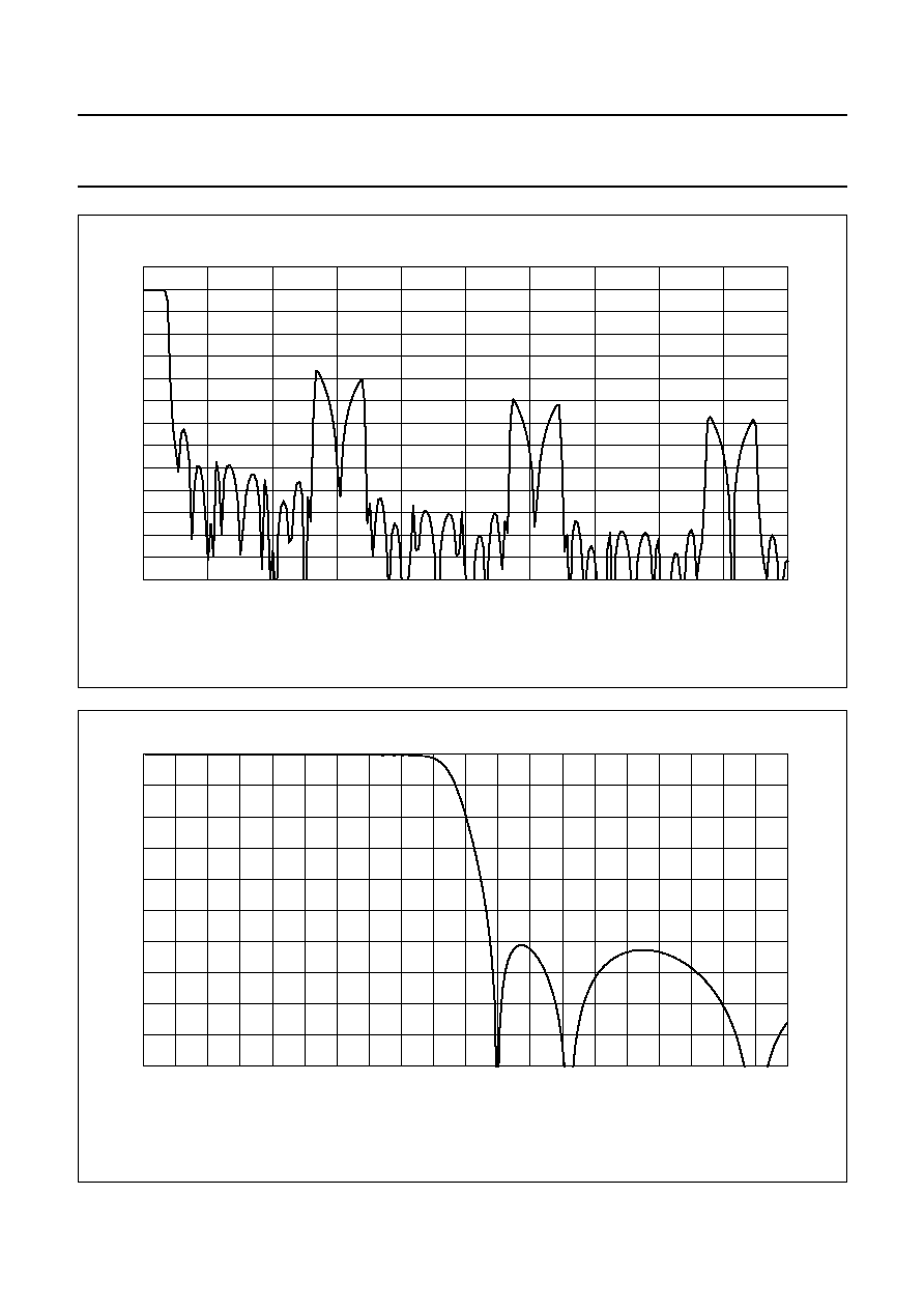
In Fig.4 the overall frequency spectrum at the DAC audio
output without external capacitor or low-pass filter for the
audio sampling frequencies of 38 kHz is shown. In Fig.5
the detailed spectrum around f
s
is shown for an f
s
of
38, 44.1 and 48 kHz. The pass band bandwidth (
-
3 dB) is
1
/
2
f
s
.
1999 Aug 05
12
Philips Semiconductors
Preliminary specification
Sound effects DSP
SAA7712H
Fig.4 Overall frequency spectrum audio output.
handbook, full pagewidth
500
0
-
10
-
60
0
100
MGS209
300
400
200
-
50
-
40
-
30
-
20
(dB)
f (kHz)
fs = 38000 Hz
Fig.5 Detailed frequency spectrum audio output.
handbook, full pagewidth
0
0
10000
30000
MGS210
20000
-
10
-
50
-
40
-
30
-
20
f (Hz)
fs = 38000 Hz
0
11605
34816
23211
fs = 44100 Hz
0
12632
37895
25263
fs = 48000 Hz
(dB)

1999 Aug 05
13
Philips Semiconductors
Preliminary specification
Sound effects DSP
SAA7712H
8.1.5
P
ERFORMANCE
The signed-magnitude noise-shaped DAC has a dynamic
range in excess of 100 dB. The signal-to-noise ratio of the
audio output at full-scale is determined by the word length
of the converter. The noise at low outputs is fully
determined by the noise performance of the DAC. Since it
is a signed-magnitude type, the noise at digital silence is
also low. As a disadvantage, the total THD is higher than
conventional DACs. The typical total harmonic
distortion-plus-noise to signal ratio as a function of the
output level is shown in Fig.6.
Fig.6
Typical (THD + N)/S curve as a function of
the output level.
handbook, halfpage
-
80
-
60
-
40
0
MGS211
-
20
-
60
-
80
-
40
-
20
(THD
+
N)/S
(dB)
output level (dB)
8.1.6
P
OWER
-O
N
M
UTE
(POM)
To avoid any uncontrolled noise at the audio outputs after
power-on of the IC, the reference current source of the
DAC is switched off. The capacitor on pin POM
determines the time after which this current has a soft
switch-on. So at power-on the current audio signal outputs
are always muted. The loading of the external capacitor is
done in two stages via two different current sources.
The loading starts at a current level that is 9 times lower
than the current loading after the voltage on pin POM has
passed the 1 V level. This results in an almost dB linear
behaviour.
8.1.7
P
OWER
-
OFF PLOP SUPPRESSION
Power should still be provided to the analog part of the
DAC, while the digital part is switching off. As a result, the
output voltage will decrease gradually allowing the power
amplifier some extra time to switch-off without audible
plops. If a 5 V power supply is present, the supply voltage
of the analog part of the DAC can be fed from the 5 V
power supply via a 1.8 V zener diode. A capacitor,
connected to the 3.3 V power supply, provides power to
the analog part when the 5 V power supply is switching off
fast.

1999 Aug 05
14
Philips Semiconductors
Preliminary specification
Sound effects DSP
SAA7712H
8.1.8
P
IN
VREFDA
With two internal resistors half the supply voltage (V
DDA2
)
is obtained and coupled to an internal buffer. This
reference voltage is used as DC voltage for the output
operational amplifiers and as reference for the DAC.
In order to obtain the lowest noise and to have the best
ripple rejection, a filter capacitor has to be added between
this pin and ground.
8.1.9
I
NTERNAL
DAC
CURRENT REFERENCE
As a reference for the internal DAC current and for the
DAC current source output, a current is drawn from the
level on pin VREFDA to pin V
SSA2
(ground) via an internal
resistor. The absolute value of this resistor also
determines the absolute current of the DAC. This means
that the absolute value of the current is not that fixed due
to the spread of the current reference resistor value. This,
however, does not influence the absolute output voltages
because these voltages are also derived from a
conversion of the DAC current to the actual output voltage
via internal resistors.
8.1.10
S
UPPLY OF THE ANALOG OUTPUTS
All the analog circuitry of the DACs and the operational
amplifiers are fed by 2 supply pins, V
DDA2
and V
SSA2
.
Pin V
DDA2
must have sufficient decoupling to prevent THD
degradation and to ensure a good power supply rejection
ratio.
The digital part of the DAC is fully supplied from the chip
core supply.
8.2
I
2
S-bus inputs and outputs
8.2.1
D
IGITAL DATA STREAM FORMATS
For communication with external digital sources a serial
3-line bus is used. This I
2
S-bus has one line for data, one
line for clock and one line for the word select.
See Fig.7 for the general waveform formats of the four
possible formats.
The serial digital inputs (and outputs) of the SAA7712H are
capable of handling multiple formats: Philips I
2
S-bus and
LSB-justified formats of 16, 18 and 20 bits word sizes.
In Philips I
2
S-bus format, the number of bit clock (BCK)
pulses may vary in the application. When the transmitter
word length is smaller than the receiver word length, the
receiver will fill in zeroes at the LSB side. When the
transmitter word length exceeds the receiver word length,
the LSBs are skipped. For correct operation of the DACs,
there should be a minimum of 16 bit clocks per word
select.
In the LSB-justified formats, the transmitter and receiver
must be set to the same format. Be aware that a format
switch between 20, 18 and 16 bits LSB-justified formats is
done by changing the relative timing of the word select
edges. The data bits remain unchanged. In the 20 bits
format, the 2 LSBs are zeroes. In the 16 bits format, the
2 data bits following the word select edge are not zero, but
undefined. In fact, these are the LSBs of the 18-bit word.
The timing specification for the waveforms of the serial
digital inputs and outputs are given in Fig.17.
1999
Aug
05
15
Philips Semiconductors
Preliminar
y specification
Sound eff
ects DSP
SAA7712H
This text is here in white to force landscape pages to be rotated correctly when browsing through the pdf in the Acrobat reader.This text is here in
_
white to force landscape pages to be rotated correctly when browsing through the pdf in the Acrobat reader.This text is here inThis text is here in
white to force landscape pages to be rotated correctly when browsing through the pdf in the Acrobat reader. white to force landscape pages to be ...
handbook, full pagewidth
LSB-JUSTIFIED FORMAT 16 BITS
LSB-JUSTIFIED FORMAT 18 BITS
LSB-JUSTIFIED FORMAT 20 BITS
INPUT FORMAT I
2
S-BUS
WS
LEFT
LEFT
LEFT
LEFT
RIGHT
RIGHT
RIGHT
RIGHT
3
2
2
2
15
16
17
18
1
15
16
1
1
3
2
1
MSB
B2
MSB
MSB
B2
MSB
LSB
B2
MSB
B2
B3
B4
B15
LSB
B17
2
15
16
17
18
1
MSB
B2
B3
B4
LSB
B17
2
15
16
17
18
19
20
1
MSB
B2
B3
B4
B5
B6
LSB
B19
MGS212
2
15
16
17
18
19
20
1
MSB
B2
B3
B4
B5
B6
LSB
B19
2
15
16
1
MSB
LSB
B2
B15
BCK
DATA
WS
BCK
DATA
WS
BCK
DATA
WS
BCK
DATA
Fig.7 All serial data I/O formats.

1999 Aug 05
16
Philips Semiconductors
Preliminary specification
Sound effects DSP
SAA7712H
8.2.2
S
LAVE
I
2
S-
BUS INPUTS
The SAA7712H has two slave I
2
S-bus inputs, I
2
S_IN1 and
I
2
S_IN2 with respective data lines I
2
S_IN1_DATA and
I
2
S_IN2_DATA, word select lines I
2
S_IN1_WS and
I
2
S_IN2_WS and bit clock lines I
2
S_IN1_BCK and
I
2
S_IN2_BCK. The external source is master and supplies
the bit clock and word select. The I
2
C-bus bits
audio_format(2 to 0) allow for selection of the desired
I
2
S-bus format (see Table 13). The bits, needed for
selecting a certain format, are explained in Table 2.
The input circuitry is limited in handling the number of BCK
pulses per WS period. If the word rate of the selected
digital input source is f
s
, the bit clock must be a continuous
clock in the range of 16f
s
f
bit(CLK)
256f
s
. The minimum
limit of the audio sample frequency is determined by
1
/
18
f
SCL
. The maximum limit of the audio sample frequency
is determined by DSP_clock/481 Hz.
Table 2
I
2
C-bus audio_format mode bits (0FF9H,
see Table 13)
The selection of the DSP input among the decimated
analog input and the I
2
S-bus inputs I
2
S_IN1 and I
2
S_IN2
is controlled with I
2
C-bus bit audio_source (see Table 13).
The meaning of this bit can be found in Table 3.
AUDIO_FORMAT
OUTPUT
BIT 9
BIT 8
BIT 7
0
0
0
internal format (for test
purposes only)
-
0
1
LSB-justified, 16 bits
-
1
0
LSB-justified, 18 bits
-
1
1
LSB-justified, 20 bits
1
0
0
standard I
2
S-bus (default)
Table 3
I
2
C-bus audio_source mode bit (0FF9H,
see Table 13)
8.2.3
M
ASTER
I
2
S-
BUS INPUTS AND OUTPUTS
For the co-processor I/O interface, the SAA7712H acts as
a master. The SAA7712H supplies both the bit clock and
word select. The I
2
C-bus bits host_io_format(1 and 0)
allow for selection of the desired I
2
S-bus format (see
Table 13).
The bits needed for selecting a certain format are given in
Table 4.
All I
2
S-bus output lines, I
2
S_IO_WS, I
2
S_IO_BCK,
I
2
S_IO_OUT1 and I
2
S_IO_OUT2, can be 3-stated with
I
2
C-bus bit en_host_io (see Table 13).
The word select and bit clock of the co-processor I/O
interface are derived from the word select and bit clock of
the audio source selected according to Table 3.
The incoming bit clock can be divided by 1, 2, 4 or 8
depending on the needs of an external connected
co-processor. These selections can be done with I
2
C-bus
bits cloop_mode(2 to 0) (see Table 13). The meaning of
these bits is shown in Table 5.
AUDIO_SOURCE
OUTPUT
Bit 5
0
I
2
S_IN1 (default)
1
I
2
S_IN2

1999 Aug 05
17
Philips Semiconductors
Preliminary specification
Sound effects DSP
SAA7712H
Table 4
I
2
C-bus host_io_format bits (0FF9H, see Table 13)
Table 5
I
2
C-bus cloop_mode bits (0FF9H, see Table 13)
HOST_IO_FORMAT
OUTPUT
BIT 11
BIT 10
0
0
standard I
2
S-bus (default)
0
1
LSB-justified format, 16 bits
1
0
LSB-justified format, 18 bits
1
1
LSB-justified format, 20 bits
CLOOP_MODE
OUTPUT
BIT 15
BIT 14
BIT 13
0
-
-
bypass WS (default)
1
-
-
WS 50% duty factor
-
0
0
bypass BCLK (default)
-
0
1
divide BCLK by 2
-
1
0
divide BCLK by 4
-
1
1
divide BCLK by 8
8.3
Equalizer accelerator
8.3.1
I
NTRODUCTION
The equalizer accelerator is a hardware accelerator to the
DSP core. Both its inputs and outputs are stored in
registers of the DSP core.
The equalizer cannot be used and cannot be programmed
if no word select and bit clock signal are present on a
selected digital source input; see audio_source bit in
Table 3 (I
2
S_IN1 or I
2
S_IN2). The minimum required
DSP_clock is 481f
s
.
The equalizer accelerator contains one second-order filter
data path that is 20 times multiplexed. With this circuit, a
2-channel equalizer of 10 second-order sections per
channel or a 4-channel equalizer of 5 second-order
sections per channel can be realised. The centre
frequency, gain and Q-factor of all 20 second-order
sections can be set independently from each other. Every
section is followed by a selectable attenuation of 0 or 6 dB.
Per section, 4 bytes of the I
2
C-bus register are needed to
store the settings. The equalizer settings can be updated
during normal operation. An application program supports
the programming of the equalizer.
If the gain setting causes the audio signal to exceed the
maximum level in one of the filter sections, the signal will
be clipped and the equalizer overflow output (pin EQOV)
will be set HIGH until the end of the next audio sample
period.
8.3.2
C
ONFIGURATION OF EQUALIZER SECTIONS
The equalizer accelerator can make a 2-channel equalizer
of 10 second-order sections per channel or a 4-channel
equalizer of 5 second-order sections per channel.
The sections of one channel can be chained one after the
other. Depending on the I
2
C-bus control bit two_four
(see Table 11), the 20 filter sections are combined for the
appropriate configuration, as illustrated in Fig.8.

1999 Aug 05
18
Philips Semiconductors
Preliminary specification
Sound effects DSP
SAA7712H
Fig.8 Configurations of the equalizer sections.
handbook, full pagewidth
MGS213
OUT0
IN0
2 channel
2 channel
1
A
2
3
4
5
OUT1
IN1
B
OUT2
IN2
C
OUT3
IN3
D
8.3.3
O
VERFLOW DETECTION
The equalizer has an overflow flag. This flag is fed to
output pin EQOV. If an overflow is detected in one of the
filter sections, the signal is clipped to the maximum
allowed level. The overflow flag is immediately set.
It remains at a HIGH-level during the remaining part of the
current audio sample period and for the whole next sample
period. If no overflow is detected during this next sample
period, the overflow flag goes to a LOW-level at the
beginning of the sample period after that. Otherwise, the
overflow flag remains at a HIGH-level for at least one other
audio sample period.
8.4
Clock circuit and oscillator
8.4.1
G
ENERAL DESCRIPTION
The chip has a crystal clock oscillator. It can use a crystal
at either f
xtal
= 16.384 MHz = 512
◊
32 kHz or
f
xtal
= 18.432 MHz = 576
◊
32 kHz in fundamental mode.
The block diagram of this Pierce oscillator is shown in
Fig.9. The active element needed to compensate for the
loss resistance of the crystal is the block Gm. This block is
placed between the external pins OSC_IN
and OSC_OUT.
The gain of the oscillator is internally controlled by the
AGC block. A sine wave with a peak-to-peak voltage close
to the oscillator power supply voltage is generated.
The AGC block prevents clipping of the sine wave and
therefore the higher harmonics are as low as possible.
At the same time, the voltage of the sine wave is as high
as possible so reducing the jitter going from sine wave to
clock signal. The sinusoidal output is converted into a
CMOS compatible clock by the comparator.
The second mode of operation shown in Fig.10, is the
slave mode which is driven by a master clock directly.
The signal to pin OSC_IN can be driven to the power
supply voltages V
DD_OSC
and V
SS_OSC
.
8.4.2
S
UPPLY OF THE CRYSTAL OSCILLATOR
The power supply connections of the oscillator are
separate from the other supply lines. This is to minimize
the feedback from the ground bounce of the chip to the
oscillator circuit. Pin V
SS_OSC
is used as the ground supply
and pin V
DD_OSC
as the positive supply.
1999 Aug 05
19
Philips Semiconductors
Preliminary specification
Sound effects DSP
SAA7712H
Fig.9 Block diagram of the crystal oscillator circuit.
handbook, full pagewidth
MGS214
clock out
OSC_OUT
Rbias
100 k
VDD_OSC
0.5VDD_OSC
VSS_OSC
off chip
on chip
61
64
63
OSC_IN
C1
10 pF
C2
10 pF
62
Gm
AGC
Fig.10 Block diagram of the oscillator in slave mode.
handbook, full pagewidth
MGS215
clock out
OSC_OUT
Rbias
100 k
VDD_OSC
0.5VDD_OSC
VSS_OSC
off chip
slave input
on chip
61
64
63
OSC_IN
C1
10 pF
C3
5 pF
C2
10 pF
62
Gm
AGC

1999 Aug 05
20
Philips Semiconductors
Preliminary specification
Sound effects DSP
SAA7712H
8.5
Programmable phase-locked loop circuit
The clock of the DSP is generated with a programmable PLL.
To select the required DSP clock see Table 6. The N factor (ranging from 93 to 181) can be selected with I
2
C-bus bits
PLL_div(14 to 11), see Table 10. Depending on the crystal and the required DSP clock the I
2
C-bus bits pll_fs_sel and
bits dsp_turbo must be set. The maximum limit of the audio sample frequency is determined by DSP_clock/481 Hz.
Table 6
I
2
C-bus bits PLL_div and dividing factors N of the programmable DSP clock
Notes
1. f
xtal
= 16.384 MHz; pll_fs_sel = 1 and dsp_turbo = 1, see Table 11.
2. f
xtal
= 18.432 MHz; pll_fs_sel = 1 and dsp_turbo = 1, see Table 11.
3. Usable frequency.
PLL_DIV(14 to 11)
N
DSP CLOCK FREQUENCY (MHz)
TDA9875
(1)
MSP3410D
(2)
0000
93 (default)
23.808
(3)
26.784
0001
99
25.344
(3)
28.512
0010
106
27.136
30.528
0011
113
28.928
32.544
0100
121
30.976
34.848
(3)
0101
126
32.256
36.288
(3)
0110
132
33.792
(3)
38.016
(3)
0111
137
35.072
(3)
39.456
(3)
1000
143
36.608
(3)
41.184
(3)
1001
148
37.888
(3)
42.624
(3)
1010
154
39.424
(3)
44.352
(3)
1011
159
40.704
(3)
45.792
(3)
1100
165
42.240
(3)
47.520
(3)
1101
170
43.520
(3)
48.960
(3)
1110
176
45.056
(3)
50.688
(3)
1111
181
46.336
(3)
52.128
(3)
1999 Aug 05
21
Philips Semiconductors
Preliminary specification
Sound effects DSP
SAA7712H
8.6
I
2
C-bus control
8.6.1
I
NTRODUCTION
A general description of the I
2
C-bus format can be
obtained from Philips Semiconductors, International
Marketing and Sales Communications (IMSC).
For the external control of the SAA7712H a fast I
2
C-bus
is implemented. This is a 400 kHz bus which is downward
compatible with the standard 100 kHz bus.
There are different types of control instructions:
∑
Instructions to control the DSP program, program the
coefficient RAM and read the values of parameters
∑
Instructions to control the equalizer, program the
equalizer coefficient RAM to be able to change the
centre frequency, gain and Q-factor of the equalizer
sections
∑
Instructions to control the source selection and
programmable parts, e.g. PLL clock speed.
The detailed description of the I
2
C-bus and commands is
given in the following sections. The description of the
different bits in the memory map is given in Section 9.6.
The equalizer cannot be used and cannot be
programmed if there is no word select and bit clock signal
present on a selected digital source input; see
audio_source bit in Table 3 (I
2
S_IN1 and I
2
S_IN2).
The minimum limit of the audio sample frequency is
determined by
1
/
18
f
SCL
.
8.6.2
C
HARACTERISTICS OF THE
I
2
C-
BUS
The I
2
C-bus is for 2-way, 2-line communication between
different ICs or modules. The two lines are a serial data
line (SDA) and a serial clock line (SCL). Both lines must
be connected to V
DD
via a pull-up resistor when
connected to the output stages of a microcontroller. For a
400 kHz I
2
C-bus the recommendation from Philips
Semiconductors must be followed (e.g. up to loads of
200 pF on the bus a pull-up resistor can be used, between
200 to 400 pF a current source or switched resistor must
be used). Data transfer can only be initiated when the bus
is not busy.
8.6.3
B
IT TRANSFER
One data bit is transferred during each clock pulse.
The data on the SDA line must remain stable during the
HIGH period of the clock pulse as changes in the data line
at this time will be interpreted as control signals
(see Fig.11). The maximum clock frequency is 400 kHz.
To be able to run on this high frequency all the inputs and
outputs connected to this bus must be designed for this
high speed I
2
C-bus according to the Philips specification.
Fig.11 Bit transfer on the I
2
C-bus.
handbook, full pagewidth
MGS216
SDA
SCL
data line
stable;
data valid
change
of data
allowed

1999 Aug 05
22
Philips Semiconductors
Preliminary specification
Sound effects DSP
SAA7712H
8.6.4
S
TART AND STOP CONDITIONS
Both data and clock lines will remain HIGH when the bus is not busy. A HIGH-to-LOW transition of the data line, while
the clock is HIGH, is defined as a START condition (S). A LOW-to-HIGH transition of the data line while the clock is HIGH
is defined as a STOP condition (P) (see Fig.12).
Fig.12 START and STOP conditions.
handbook, full pagewidth
MGS217
SDA
SCL
S
P
START condition
STOP condition
8.6.5
D
ATA TRANSFER
A device generating a message is a `transmitter' and a device receiving a message is the `receiver'. The device that
controls the message is the `master' and the devices which are controlled by the master are the `slaves'.
Fig.13 Data transfer on the I
2
C-bus.
handbook, full pagewidth
MGS218
SDA
SCL
S
START condition
1
2
7
8
9
1
2
3 to 8
9
MSB
ACK
ACK
acknowledgement
signal from receiver
byte complete
interrupt within receiver
clock line held LOW while
interrupts are serviced
acknowledgement
signal from receiver
1999 Aug 05
23
Philips Semiconductors
Preliminary specification
Sound effects DSP
SAA7712H
8.6.6
A
CKNOWLEDGE
The number of data bits transferred between the START
and STOP conditions from the transmitter to the receiver
is not limited. Each byte of eight bits is followed by one
acknowledge bit (see Fig.13). The acknowledge bit is a
HIGH-level left on the bus by the transmitter whereas the
master generates an extra acknowledge related clock
pulse.
A slave receiver which is addressed must generate an
acknowledge after the reception of each byte. Also a
master must generate an acknowledge after the reception
of each byte that has been clocked out of the slave
transmitter. The device that acknowledges has to pull
down the SDA line (left HIGH by the transmitter) during the
acknowledge clock pulse, so that the SDA line is stable
LOW during the HIGH period of the acknowledge related
clock pulse.
Set-up and hold times must be taken into account.
A master receiver must signal an end of data to the
transmitter by not generating an acknowledge on the last
byte that has been clocked out of the slave. In this event
the transmitter must leave the data line HIGH to enable the
master to generate a STOP condition (see Fig.14).
8.6.7
S
TATE OF THE
I
2
C-
BUS INTERFACE DURING AND
AFTER
P
OWER
-
ON RESET
During reset (see Section 8.8), the internal SDA line is kept
HIGH and pin SDA is therefore high-impedance. The SDA
line remains HIGH until a master pulls it down to initiate
communication.
Fig.14 Acknowledge on the I
2
C-bus.
handbook, full pagewidth
MGS219
S
START condition
1
2
7
8
9
data output
by receiver
SCL from
master
clock pulse for
acknowledgement
data output
by transmitter
acknowledge
not acknowledge

1999 Aug 05
24
Philips Semiconductors
Preliminary specification
Sound effects DSP
SAA7712H
8.7
External control pins
For external control two input pins are implemented.
The status of these pins can be changed by applying a
logic level. The status of these pins is recorded in the
internal status register. The function of each input pin is
determined by the DSP software.
Pin DSP_IN1:
∑
Logic 0 or left open-circuit means volume coefficients
updates are possible (default)
∑
Logic 1 means no updates of volume coefficients are
possible.
Pin DSP_IN2:
∑
If the 3-band spectrum analyser is used:
≠ Logic 1 will reset the band registers of the analyser
≠ Logic 0 or left open-circuit means no reset of the
band registers will be done (default).
∑
If the 3-band spectrum analyser is not used:
≠ The state of pin DSP_IN2 can be read via an I
2
C-bus
command.
To control external devices two output pins are
implemented. The status of these pins is controlled by the
DSP program. The functions of these pins are determined
by the DSP software.
Pin DSP_OUT1:
∑
To drive pin DSP_OUT1 via an I
2
C-bus command.
Pin DSP_OUT2:
∑
To drive pin DSP_OUT2 via an I
2
C-bus command.
8.8
Reset pin
The reset signal on pin DSP_RESET is active LOW and
has an internal pull-up resistor. Between this pin and
ground a capacitor should be connected to allow a proper
switch-on of the supply voltage. The capacitor value is
such that the chip is in the reset state as long as the power
supply is not stabilized.
A more or less fixed relationship between the
DSP_RESET time constant and the POM time constant is
obligatory. The voltage on pin POM determines the current
flowing in the DACs. For 0 V on pin POM, the DAC
currents are zero and so also the DACs output voltages.
When a 3 V supply voltage (V
DDA2
) is supplied to pin POM,
the DAC currents are at their nominal (maximum) value.
Long before the DAC outputs get their nominal output
voltages, the DSP must be in normal operating mode to
reset the output register. Therefore, the time constant of
DSP_RESET must be shorter than the time constant of
POM. For advised capacitors see the application diagram.
The reset has the following function:
∑
All I
2
C-bus registers are reset to their default values
∑
The DSP algorithm is re-started
∑
The external control output pins are reset
(see Section 8.7)
∑
Pin SDA is high-impedance.
When the level on the reset pin is HIGH, the DSP algorithm
starts to run.
In addition to the reset pin, there is also a software reset;
bit PC_reset (bit 15, 0FFDH, see Table 11). This reset has
the following function:
∑
The DSP algorithm is re-started
∑
The external control output pins are reset
(see Section 8.7).

1999 Aug 05
25
Philips Semiconductors
Preliminary specification
Sound effects DSP
SAA7712H
8.9
Power supply connection and EMC
The digital part of the chip has in total 5 positive supply line
connections and 8 ground connections. To minimise
radiation the chip should be put on a double layer PCB with
a large ground plane on one side. The ground supply lines
should have a short connection to this ground plane. A coil
and capacitor network in the positive supply line can be
used as high frequency filter.
8.10
Test mode connections
Pins TSCAN, RTCB and SHTCB are used to put the chip
in test mode and to test the internal connections. Each pin
has an internal pull-down resistor to ground. In the
application these pins can be left open-circuit or connected
to ground.
9
I
2
C-BUS FORMAT
9.1
Addressing
Before any data is transmitted on the I
2
C-bus, the device
which should respond is addressed first. The addressing is
always done with the first byte transmitted after the START
procedure.
9.2
Slave address (pin A0)
The SAA7712H acts as a slave receiver or a slave
transmitter. Therefore, the clock signal SCL is only an
input signal. The data signal SDA is a bidirectional line.
The slave address is shown in Table 7.
Table 7
Slave address
The subaddress bit A0 corresponds to the hardware
address pin A0 which allows the device to have two
addresses. This allows the control of two SAA7712Hs via
the same I
2
C-bus.
MSB
LSB
0
0
1
1
1
1
A0
R/W
9.3
Write cycles
The I
2
C-bus configuration for a write cycle is shown in
Fig.15. The write cycle is used to write the bytes to control
the PLL for the DSP clock generation, the format of the
I
2
S-bus and some other settings. More details can be
found in the I
2
C-bus memory map (see Table 8).
The data length is 2 or 3 bytes, depending on the
accessed memory. The slave receiver detects the address
and adjusts the number of bytes accordingly. For XRAM,
the data word length is 18 bits and 3 bytes are sent over
the I
2
C-bus. The upper 6 bits (i.e. bit 7 to bit 2) of the first
byte DATA H are don't care. For YRAM, the data word
length is 12 bits and 2 bytes are sent over the I
2
C-bus. The
left nibble (i.e. bit 7 to bit 4) of the first byte DATA H is don't
care.
9.4
Read cycles
The I
2
C-bus configuration for a read cycle is shown in
Fig.16. The read cycle is used to read the data values from
XRAM or YRAM. The master starts with a START
condition (S), the SAA7712H address `0011110' and a
logic 0 (write) for the read/write bit. This is followed by an
acknowledge of the SAA7712H. The master then writes
the memory high address and memory low address where
the reading of the memory content of the SAA7712H must
start. The SAA7712H acknowledges these addresses
both.
The master than generates a repeated START and again
the SAA7712H address `0011110' but this time followed
by a logic 1 (read) of the read/write bit. From this moment
on, the SAA7712H will send the memory content in groups
of 2 (YRAM) or 3 (XRAM) bytes to the I
2
C-bus, each time
acknowledged by the master. The master stops this cycle
by generating a negative acknowledge, then the
SAA7712H frees the I
2
C-bus and the master can generate
a STOP condition (P).

1999
Aug
05
26
Philips Semiconductors
Preliminar
y specification
Sound eff
ects DSP
SAA7712H
This text is here in white to force landscape pages to be rotated correctly when browsing through the pdf in the Acrobat reader.This text is here in
_
white to force landscape pages to be rotated correctly when browsing through the pdf in the Acrobat reader.This text is here inThis text is here in
white to force landscape pages to be rotated correctly when browsing through the pdf in the Acrobat reader. white to force landscape pages to be ...
0 1 1 1 0 0 0
A
C
K
A
C
K
A
C
K
A
C
K
A
C
K
address
S
0
ADDR H
ADDR L
DATA H
DATA M
R/W
MGD568
auto increment if repeated n-groups of 3 (2) bytes
P
A
C
K
DATA L
Fig.15 Master transmitter writes to the DSP registers.
S = START condition.
ACK = acknowledge from DSP (SDA LOW).
ADDR H and ADDR L = address DSP register.
DATA H, DATA M and DATA L = data of XRAM or registers.
DATA H and DATA M = data of YRAM.
P = STOP condition.
0 1 1 1 0 0 0
A
C
K
A
C
K
A
C
K
A
C
K
A
C
K
address
S
0
0 1 1
1
1 0 0
S
0
ADDR H
ADDR L
DATA H
R/W
MGA808 - 1
auto increment if repeated n-groups of 3 (2) bytes
P
A
C
K
A
C
K
DATA M
DATA L
R/W
Fig.16 Master transmitter reads from the DSP registers.
S = START condition.
ACK = acknowledge from DSP (SDA LOW).
ADDR H and ADDR L = address DSP register.
DATA H, DATA M and DATA L = data of XRAM or registers.
DATA H and DATA M = data of YRAM.
P = STOP condition.

1999 Aug 05
27
Philips Semiconductors
Preliminary specification
Sound effects DSP
SAA7712H
9.5
I
2
C-bus memory map summary
The I
2
C-bus memory map contains all defined I
2
C-bus bits. The map is split into two different sections: hardware memory
registers and the RAM definitions. The preliminary memory map is given in Table 8.
Table 8
I
2
C-bus memory map
Table 9
I
2
C-bus memory map: overview of various settings
9.6
I
2
C-bus memory map details
Table 10 I
2
C_DCS_CTR register (0FFFH)
SUBADDRESSES
FUNCTION
SIZE
0FF9H to 0FFFH
various settings (see Table 9)
4
◊
16 bits
0F80H to 0FA7H
equalizer
40
◊
16 bits
0800H to 097FH
YRAM
384
◊
12 bits
0000H to 017FH
XRAM
384
◊
18 bits
REGISTER NAME
SUBADDRESS
I
2
C_DCS_CTR
0FFFH (see Table 10)
I
2
C_ADDA
0FFDH (see Table 11)
I
2
C_SEL
0FFAH (see Table 12)
I
2
C_HOST
0FF9H (see Table 13)
NAME
SIZE
(BITS)
DESCRIPTION
DEFAULT
BIT POSITION
-
10
reserved
9 to 0
loopo_on_off
1
pin SYS_CLK output enable: on (logic 1) or off (logic 0) off
10
PLL_div
4
PLL clock division factor for DSP_clock (see Table 6)
93
14 to 11
-
1
reserved
15

1999 Aug 05
28
Philips Semiconductors
Preliminary specification
Sound effects DSP
SAA7712H
Table 11 I
2
C_ADDA register (0FFDH)
Table 12 I
2
C_SEL register (0FFAH)
Table 13 I
2
C_HOST register (0FF9H)
NAME
SIZE
(BITS)
DESCRIPTION
DEFAULT
BIT
POSITION
-
10
reserved
9 to 0
pll_fs_sel
1
divide oscillator by 2 (logic 1)
division
10
dsp_turbo
1
double DSP_clock (logic 1)
doubling
11
two_four
1
2-channel 10-band (logic 1) or 4-channel 5-band (logic 0)
equalizer configuration
4-channel
5-band
12
-
2
reserved
14 and 13
pc_reset
1
re-start DSP algorithm (logic 1) or DSP running (logic 0)
DSP running
15
NAME
SIZE
(BITS)
DESCRIPTION
DEFAULT
BIT
POSITION
-
8
reserved
7 to 0
bypass_pll
1
bypass PLL used for DSP_clock (logic 1) or use PLL for
DSP_clock (logic 0)
use PLL
8
-
4
reserved
12 to 9
inv_host_ws
1
inverting (logic 1) or non-inverting (logic 0) word select
non-inverting
13
-
2
reserved
15 and 14
NAME
SIZE
(BITS)
DESCRIPTION
DEFAULT
BIT
POSITION
-
5
reserved
4 to 0
audio_source
1
input source is I
2
S_IN1 or I
2
S_IN2 (see Table 3)
I
2
S_IN1
5
-
1
reserved
6
audio_format
3
format of selected input source (see Table 2)
standard I
2
S-bus 9 to 7
host_io_format
2
host input/output data format (see Table 4)
standard I
2
S-bus 11 and 10
en_host_io
1
enable (logic 1) or disable (logic 0) co-processor I
2
S-bus
disable
12
cloop_mode
3
cloop mode (see Table 5)
bypass WS
15 to 13

1999 Aug 05
29
Philips Semiconductors
Preliminary specification
Sound effects DSP
SAA7712H
10 LIMITING VALUES
In accordance with the Absolute Maximum Ratings system (IEC 134).
Notes
1. Human body model: equivalent to discharging a 100 pF capacitor through a 1.5 k
resistor.
2. Machine model: equivalent to discharging a 200 pF capacitor through a 2.5
µ
H inductance and a 0
series resistor.
11 THERMAL CHARACTERISTICS
Note
1. Printed-circuit board mounting.
SYMBOL
PARAMETER
CONDITION
MIN.
MAX.
UNIT
V
DD3V
supply voltage 3.3 V analog and
digital
-
0.5
+5
V
V
DD5V
supply voltage 5 V periphery
only valid for the voltages in
connection with the 5 V I/Os
-
0.5
+6.5
V
V
DD
voltage difference between two
V
DDx
pins
-
550
mV
I
IK
input clamping diode current
V
i
<
-
0.5 V or V
i
> V
DD
+ 0.5 V
-
10
mA
I
O(sink/source)
output sink or source current,
output type 4 mA
-
0.5 V < V
o
< V
DD
+ 0.5 V
-
20
mA
I
DD
,I
SS
V
DD
or V
SS
current per supply
pin
-
750
mA
T
amb
ambient temperature
0
70
∞
C
T
stg
storage temperature
-
65
+150
∞
C
V
es
electrostatic handling voltage for
all pins
note 1
-
3000
+3000
V
note 2
-
300
+300
V
I
lu(prot)
latch-up protection
CIC specification/test method
100
-
mA
P/out
power dissipation per output
-
100
mW
P
tot
total power dissipation
-
400
mW
SYMBOL
PARAMETER
CONDITION
VALUE
UNIT
R
th(j-a)
thermal resistance from junction to ambient
in free air; note 1
45
K/W
1999 Aug 05
30
Philips Semiconductors
Preliminary specification
Sound effects DSP
SAA7712H
12 DC CHARACTERISTICS
Digital I/O at T
amb
= 0 to 70
∞
C; V
DD5V
= 4.5 to 5.5 V; V
DD3V
= 3 to 3.6 V; unless otherwise specified.
SYMBOL
PARAMETER
CONDITIONS
MIN.
TYP.
MAX.
UNIT
Supplies
V
DD3V
supply voltage 3.3 V analog
and digital
all V
DD
pins of the type VDD3
and APVVD referenced to V
SS
3
3.3
3.6
V
V
DD5V
supply voltage 5 V periphery
all V
DD
pins of the type VDD5
referenced to V
SS
4.5
5
5.5
V
3.0
3.3
3.6
V
I
DDD3V
supply current of the 3.3 V
digital core part
at f
DSP18
; maximum activity of
the DSP
-
33
80
mA
I
DDD5V
supply current of the 5 V
digital periphery part
at f
DSP18
; maximum activity of
the DSP
-
2
5
mA
I
DAC
supply current of the DACs
at zero input and output signal
-
4
7
mA
I
DD_OSC
supply current of the crystal
oscillator
at f
DSP18
; functional mode
-
3.5
3
mA
P
tot
total power dissipation
at f
DSP18
; maximum activity of
the DSP
-
135
400
mW
Logic
V
IH
HIGH-level input voltage of all
digital inputs and I/Os on
pins 24 to 29, 38, 39,
44 to 47, 57 to 60
0.7V
DDD5V
-
-
V
V
IL
LOW-level input voltage of all
digital inputs and I/Os on
pins 24 to 29, 38, 39,
44 to 47, 57 to 60
-
-
0.3V
DDD5V
V
V
hys
hysteresis voltage on pin 45
(SCL)
1
1.3
-
V
V
OH
HIGH-level output voltage of
digital outputs on pins 20, 21,
30, 33, 36, 37, 40, 41, 47, 48
I
O
=
-
4 mA
V
DDD5V
-
0.4
-
-
V
V
OL
LOW-level output voltage of
digital outputs on pins 20, 21,
30, 33, 36, 37, 40, 41, 47, 48
V
DDD5V
= 4.5 V; I
O
= 4 mA
-
-
0.4
V
V
DDD5V
= 3.0 V; I
O
= 4 mA
-
-
0.4
V
V
OL(I2C)
LOW-level output voltage of
digital I
2
C-bus data output on
pin 46 (SDA)
I
O
= 4 mA
-
-
0.4
V
I
O
output leakage current
3-state outputs on pins 21,
30, 33, 36, 37, 46 to 48
V
O
= 0 or V
DD
-
-
5
µ
A
R
pu
internal pull-up resistance to
V
DDD
on pin 57
(DSP_RESET)
23
50
80
k
1999 Aug 05
31
Philips Semiconductors
Preliminary specification
Sound effects DSP
SAA7712H
R
pd
internal pull-down resistance
to V
SSD
on pins 24 to 29, 38,
39, 44, 58 to 60
23
50
80
k
t
i(r)
, t
i(f)
input rise and fall times
V
DDD5V
= 5.5 V
-
6
200
ns
V
DDD5V
= 3.6 V
-
6
200
ns
t
LH5
output rise time on pins 20,
21, 30, 33, 36, 37, 40, 41, 47,
48
V
DDD5V
= 5.5 V;
V
DDD3V
= 3.6 V; T
j
=
-
40
∞
C
;
C
L
= 60 pF
5
-
-
ns
V
DDD5V
= 4.5 V; V
DDD3V
= 3 V;
T
j
= 125
∞
C
;
C
L
= 60 pF
-
-
25
ns
t
LH3
output rise time on pins 20,
21, 30, 33, 36, 37, 40, 41, 47,
48
V
DDD5V
= 3.6 V;
V
DDD3V
= 3.6 V; T
j
=
-
40
∞
C
;
C
L
= 60 pF
7.5
-
-
ns
V
DDD5V
= 3.0 V; V
DDD3V
= 3 V;
T
j
= 125
∞
C
;
C
L
= 60 pF
-
-
30
ns
t
LH(I2C5)
output rise time on pin 46
(SDA)
C
L
and R
pu
are application
specific
-
-
-
ns
t
LH(I2C3)
output rise time on pin 46
(SDA)
C
L
and R
pu
are application
specific
-
-
-
ns
t
HL5
output fall time on pins 20,
21, 30, 33, 36, 37, 40, 41, 47,
48
V
DDD5V
= 5.5 V;
V
DDD3V
= 3.6 V; T
j
=
-
40
∞
C
;
C
L
= 60 pF
5
-
-
ns
V
DDD5V
= 4.5 V; V
DDD3V
= 3 V;
T
j
= 125
∞
C
;
C
L
= 60 pF
-
-
25
ns
t
HL3
output fall time on pins 20,
21, 30, 33, 36, 37, 40, 41, 47,
48
V
DDD5V
= 3.6 V;
V
DDD3V
= 3.6 V; T
j
=
-
40
∞
C
;
C
L
= 60 pF
7.5
-
-
ns
V
DDD5V
= 3.0 V; V
DDD3V
= 3 V;
T
j
= 125
∞
C
;
C
L
= 60 pF
-
-
30
ns
t
HL(I2C5)
output fall time on pin 46
(SDA)
V
DDD5V
= 5.5 V;
V
DDD3V
= 3.6 V; T
j
=
-
40
∞
C
;
C
L
= 200 pF
30
-
-
ns
V
DDD5V
= 4.5 V; V
DDD3V
= 3 V;
T
j
= 125
∞
C
;
C
L
= 200 pF
-
-
300
ns
t
HL(I2C3)
output fall time on pin 46
(SDA)
V
DDD5V
= 3.6 V;
V
DDD3V
= 3.6 V; T
j
=
-
40
∞
C
;
C
L
= 200 pF
40
-
-
ns
V
DDD5V
= 3.0 V; V
DDD3V
= 3 V;
T
j
= 125
∞
C
;
C
L
= 200 pF
-
-
400
ns
SYMBOL
PARAMETER
CONDITIONS
MIN.
TYP.
MAX.
UNIT
1999 Aug 05
32
Philips Semiconductors
Preliminary specification
Sound effects DSP
SAA7712H
13 ANALOG OUTPUTS CHARACTERISTICS
T
amb
= 25
∞
C; V
DDA2
= 3.3 V; unless otherwise specified.
SYMBOL
PARAMETER
CONDITIONS
MIN.
TYP.
MAX.
UNIT
V
VREFDA
voltage on pin VREFDA
with respect to V
DDA2
-
V
SSA2
47
50
53
%
Z
VREFDA
impedance on pin VREFDA
with respect to V
DDA2
-
37
-
k
with respect to V
SSA2
-
37
-
k
V
o(rms)
AC output voltage of operational
amplifiers (RMS value)
maximum I
2
S-bus signal;
R
L
> 5 k
0.62
0.7
0.82
V
V
O(AV)
average DC output voltage of
operational amplifiers
R
L
> 5 k
1.5
1.65
1.8
V
I
pu(POML)
low pull-up current to V
DDA2
on
pin POM
voltage on pin POM < 0.6 V
3.3
-
5
µ
A
I
pu(POMH)
high pull-up current to V
DDA2
on
pin POM
voltage on pin POM > 0.8 V
50
-
75
µ
A
PSRR
DAC
power supply ripple rejection DACs
(input via I
2
S-bus)
f
ripple
= 1 kHz; V
ripple
= 100 mV
(peak value); C
VREFDA
= 22
µ
F
45
60
-
dB
I
o(max)
maximum deviation in output level
(plus or minus) of the 4 DAC
current outputs
with respect to the average of
the 4 outputs; full-scale output
-
-
0.38
dB
ct
crosstalk between all outputs in
the audio band
one output digital silence, other
three maximum volume
-
-
-
69
dB
I
o(sc)
output short-circuit current
output short-circuited to ground
-
-
20
mA
RES
DAC
DAC resolution
18
bits
(THD + N)/S total harmonic
distortion-plus-noise to signal ratio
f = 1 kHz;
V
o(ref)
= 0.72 V (RMS);
A-weighted
-
-
75
-
60
dBA
DR
DAC
dynamic range of DAC
V
o(ref)
= 0.72 V (RMS);
f = 1 kHz;
-
60 dB; A-weighted
90
96
-
dBA
DS
DAC
digital silence of DAC
f = 20 Hz
-
17 kHz;
V
o(ref)
= 0.72 V (RMS);
A-weighted
-
-
107
-
102
dBA
V
n(o)(rms)
digital silence noise level at output
(RMS value)
A-weighted
-
3
8
µ
V
d
intermodulation
distortion/comparator
f = 60 Hz and 7 kHz, ratio 4 : 1
-
-
70
-
55
dB
f
s(max)
maximum sample frequency
48
-
-
kHz
B
DAC
bandwidth DAC
at
-
3 dB
-
1
/
2
f
s
-
kHz
C
L(DAC)
load capacitance on DAC outputs
-
-
2.5
nF
R
L(DAC)
load resistance on DAC voltage
outputs
DC decoupled
5
-
-
k
1999 Aug 05
33
Philips Semiconductors
Preliminary specification
Sound effects DSP
SAA7712H
14 OSCILLATOR CHARACTERISTICS
Note
1. C
p
is the parasitic parallel capacitance of the crystal.
SYMBOL
PARAMETER
CONDITIONS
MIN.
TYP.
MAX.
UNIT
f
xtal
crystal frequency
10.000
-
19.456
MHz
f
xtal(adj)
crystal frequency variation with
adjustment
T
amb
= 25
∞
C
-
30
-
+30
ppm
f
xtal(T)
crystal frequency variation with
temperature
-
30
-
+30
ppm
f
spurious frequency attenuation
20
-
-
dB
V
xtal(M)
voltage across the crystal
(absolute peak value)
1.6
2.6
3.6
V
g
m(start)
transconductance at start-up
10.5
19
32
mS
g
m(oper)
transconductance when operating
3.6
-
38
mS
C
L
capacitive load of clock output
-
15
-
pF
N
cy(start)
number of cycles during start-up
depends on quality of the
external crystal
-
1000
-
cycles
I
xtal
supply current
at start-up
-
7
15
mA
at oscillation
-
0.6
2
mA
in slave mode
-
0.65
0.9
mA
P
xtal
drive level
at oscillation
-
0.4
0.5
mW
V
i(clk)
external clock input voltage
in slave mode
3
3.3
3.6
V
R
xtal
allowed loss resistance of the
crystal
C
p
= 5 pF
(1)
; C1 = 10 pF;
C2 = 10 pF; see Fig.9
-
20
100
R
o
output resistance
at start-up;
f
xtal
= 18.432 MHz;
V
DD_OSC
= 3.3 V
750
1300
2800

1999 Aug 05
34
Philips Semiconductors
Preliminary specification
Sound effects DSP
SAA7712H
15 I
2
S-BUS TIMING CHARACTERISTICS
Timing of the serial digital data inputs and outputs (see Fig.17).
SYMBOL
PARAMETER
MIN.
MAX.
UNIT
T
cy
bit clock cycle time
70
-
ns
t
su(D)
data set-up time (host)
32
-
ns
data set-up time (I
2
S-bus)
10
-
ns
t
h(D)
data hold time (host)
5
-
ns
data hold time (I
2
S-bus)
10
-
ns
t
su(WS)
word select set-up time (I
2
S-bus)
10
-
ns
t
h(WS)
word select hold time (I
2
S-bus)
10
-
ns
t
d(D)
data delay time (host)
-
20
ns
t
d(WS)
word select delay time (host)
-
15
ns
Fig.17 Timing definitions of the serial digital inputs and outputs.
handbook, full pagewidth
MGS220
WS IN
DATA IN
LSB
MSB
BCK
right
left
th(WS)
tr
tBCK(H)
tf
tBCK(L)
Tcy
tsu(WS)
td(WS)
td(D)
tsu(D)
th(D)
WS OUT
DATA OUT

1999 Aug 05
35
Philips Semiconductors
Preliminary specification
Sound effects DSP
SAA7712H
16 I
2
C-BUS TIMING CHARACTERISTICS
Timing of the I
2
C-bus (see Fig.18); all values referred to V
IH
and V
IL
(see Section 12).
Note
1. C
b
is the bus line capacitance in pF.
SYMBOL
PARAMETER
CONDITIONS
MIN.
MAX.
UNIT
f
SCL
SCL clock frequency
0
400
kHz
t
BUF
bus free time between a STOP and
START condition
1.3
-
µ
s
t
HD;STA
hold time (repeated) START
condition; after this period, the first
clock pulse is generated
0.6
-
µ
s
t
LOW
LOW period of the SCL clock
1.3
-
µ
s
t
HIGH
HIGH period of the SCL clock
0.6
-
µ
s
t
SU;STA
set-up time for a repeated START
condition
0.6
-
µ
s
t
HD;DAT
data hold time
0
0.9
µ
s
t
SU;DAT
data set-up time
for standard mode I
2
C-bus
system t
SU;DAT
> 250 ns
100
-
ns
t
r
rise time of both SDA and SCL
signals
f
SCL
= 400 kHz
20 + 0.1C
b
(1)
300
ns
f
SCL
= 100 kHz
20 + 0.1C
b
(1)
1000
ns
t
f
fall time of both SDA and SCL
signals
20 + 0.1C
b
(1)
300
ns
t
SU;STO
set-up time for STOP condition
0.6
-
µ
s
C
b
capacitive load for each bus line
-
400
pF
t
SP
maximum pulse width for spike
suppression
-
50
ns
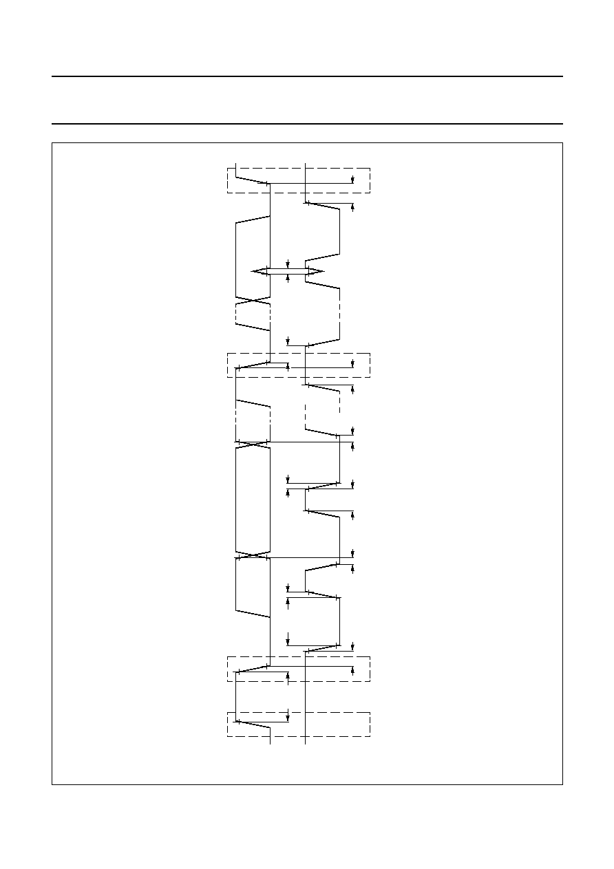
1999
Aug
05
36
Philips Semiconductors
Preliminar
y specification
Sound eff
ects DSP
SAA7712H
This text is here in white to force landscape pages to be rotated correctly when browsing through the pdf in the Acrobat reader.This text is here in
_
white to force landscape pages to be rotated correctly when browsing through the pdf in the Acrobat reader.This text is here inThis text is here in
white to force landscape pages to be rotated correctly when browsing through the pdf in the Acrobat reader. white to force landscape pages to be ...
handbook, full pagewidth
MBC611
P
S
Sr
P
tSU;STO
t SP
t HD;STA
t SU;STA
t SU;DAT
t f
t HIGH
t r
t HD;DAT
t LOW
t HD;STA
t BUF
SDA
SCL
Fig.18 Timing definition of the I
2
C-bus.
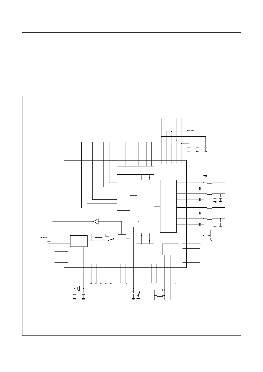
1999 Aug 05
37
Philips Semiconductors
Preliminary specification
Sound effects DSP
SAA7712H
17 APPLICATION INFORMATION
The application diagram (see Fig.19) must be considered as one of the examples of a (limited) application of the chip
e.g. in this case the I
2
S-bus inputs are not used. For the real application set-up the information of the application report
and application support by Philips are necessary on issues such as EMC, kappa reduction of the package,
DSP programming, etc.
Fig.19 Application diagram.
handbook, full pagewidth
MGS222
27
29
28
24
26
25
I
2
S_IN1_WS
I
2
S_IN1_BCK
I
2
S_IN1_DATA
I
2
S_IN2_WS
I
2
S_IN2_BCK
I
2
S_IN2_DATA
DSP
QUAD DAC
EQUALIZER
I
2
C-BUS
INTERFACE
OSCILLATOR
PLL
2
I
2
S-BUS
INPUT
SWITCH
OUT0_I
18
VDDD5V1
22
+
5 V
OUT0_V
19
OUT1_I
17
OUT1_V
16
OUT2_I
11
OUT2_V
12
OUT3_I
10
OUT3_V
HOST I/O
33
32
30
36
63
62
31
37
48
47
13
23
35
56
9
SAA7712H
I
2
S_IO_BCK
I
2
S_IO_IN1
I
2
S_IO_OUT1
I
2
S_IO_WS
I
2
S_IO_IN2
I
2
S_IO_OUT2
V
SSD5V2
42
22 nF
BLM32A07
22
nF
22
nF
22
nF
V
DDD5V3
+
5 V
34
V
DDD5V2
52
V
DDD3V1
53
V
DDD3V2
+
3 V
+
3 V
+
3 V
14
V
DDA2
V
SSD5V1
TEST2
TEST1
V
SSD3V6
44
45
46
SDA
57
DSP_RESET
SCL
A0
V
SSA2
OSC_OUT
OSC_IN
100
1.8 nF
OUT0
100
1.8 nF
OUT1
10 nF
10 nF
+
5 V
100
1.8 nF
OUT2
100
1.8 nF
OUT3
VREFDA
15
10 nF
10 nF
22
µ
F
1
µ
F
POM
8
4.7
µ
F
43
49
50
51
V
SSD3V2
V
SSD3V1
V
SSD3V3
V
SSD5V3
54
55
V
SSD3V5
V
SSD3V4
DSP_IN2
39
DSP_OUT1
40
DSP_OUT2
41
EQOV
20
58
RTCB
59
SHTCB
64
61
60
TSCAN
4.7 k
4.7 k
DSP_IN1
38
100 nF
10 pF
10 pF
11.2896 MHz
+
5 V
21
SYS_CLK
VDD_OSC
VSS_OSC
BLM32A07
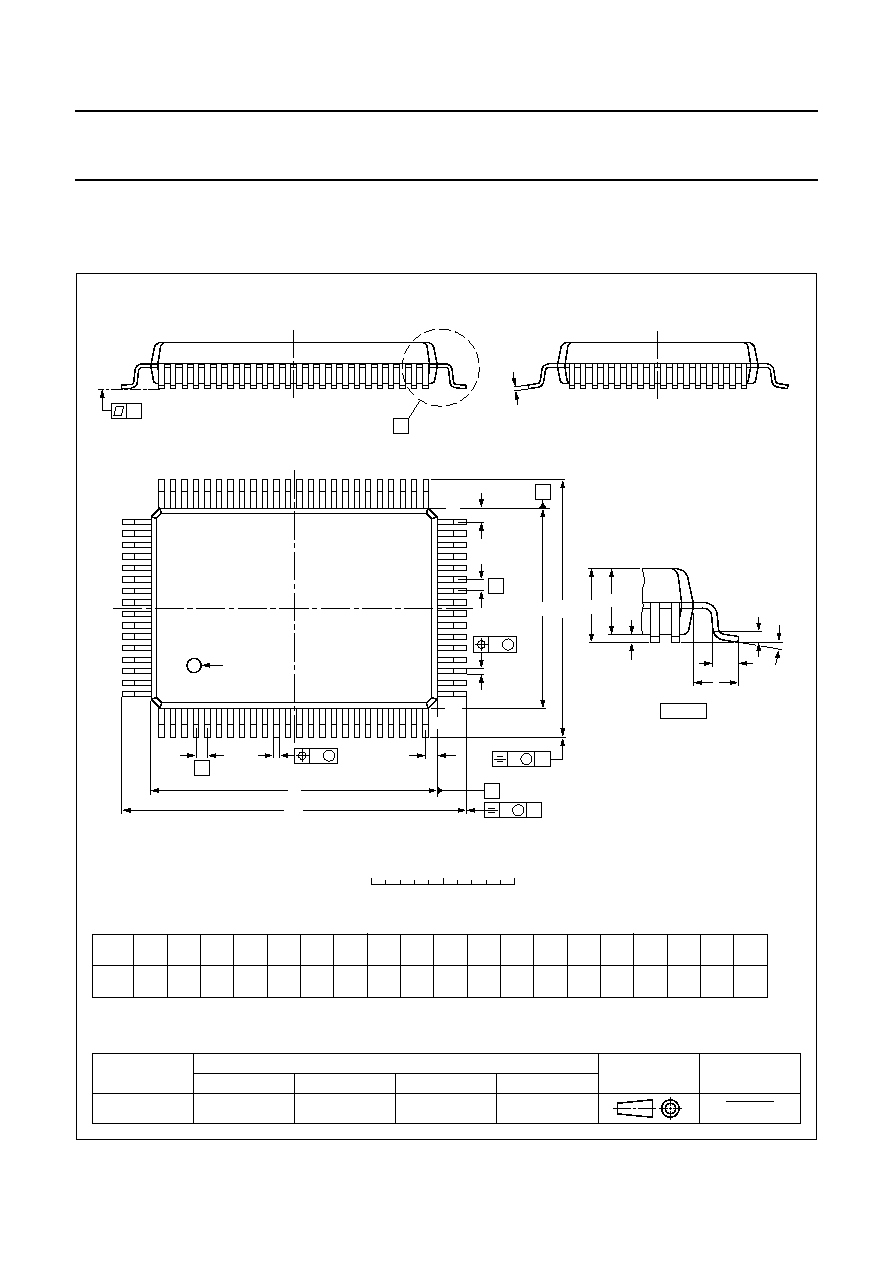
1999 Aug 05
38
Philips Semiconductors
Preliminary specification
Sound effects DSP
SAA7712H
18 PACKAGE OUTLINE
UNIT
A
1
A
2
A
3
b
p
c
E
(1)
e
H
E
L
L
p
Z
y
w
v
REFERENCES
OUTLINE
VERSION
EUROPEAN
PROJECTION
ISSUE DATE
IEC
JEDEC
EIAJ
mm
0.36
0.10
2.87
2.57
0.25
0.45
0.30
0.25
0.13
14.1
13.9
0.8
18.2
17.6
1.2
0.8
7
0
o
o
0.2
0.1
0.2
1.95
DIMENSIONS (mm are the original dimensions)
Note
1. Plastic or metal protrusions of 0.25 mm maximum per side are not included.
1.0
0.6
SOT318-1
95-02-04
97-08-01
D
(1)
(1)
(1)
20.1
19.9
H
D
24.2
23.6
E
Z
1.0
0.6
D
b
p
e
E
A
1
A
L
p
detail X
L
(A )
3
B
24
c
b
p
E
H
A
2
D
H
v
M
B
D
Z D
A
Z E
e
v
M
A
1
80
65
64
41
40
25
pin 1 index
X
y
w
M
w
M
0
5
10 mm
scale
80 leads (lead length 1.95 mm); body 14 x 20 x 2.7 mm; high stand-off height
QFP80: plastic quad flat package;
SOT318-1
A
max.
3.3

1999 Aug 05
39
Philips Semiconductors
Preliminary specification
Sound effects DSP
SAA7712H
19 SOLDERING
19.1
Introduction to soldering surface mount
packages
This text gives a very brief insight to a complex technology.
A more in-depth account of soldering ICs can be found in
our
"Data Handbook IC26; Integrated Circuit Packages"
(document order number 9398 652 90011).
There is no soldering method that is ideal for all surface
mount IC packages. Wave soldering is not always suitable
for surface mount ICs, or for printed-circuit boards with
high population densities. In these situations reflow
soldering is often used.
19.2
Reflow soldering
Reflow soldering requires solder paste (a suspension of
fine solder particles, flux and binding agent) to be applied
to the printed-circuit board by screen printing, stencilling or
pressure-syringe dispensing before package placement.
Several methods exist for reflowing; for example,
infrared/convection heating in a conveyor type oven.
Throughput times (preheating, soldering and cooling) vary
between 100 and 200 seconds depending on heating
method.
Typical reflow peak temperatures range from
215 to 250
∞
C. The top-surface temperature of the
packages should preferable be kept below 230
∞
C.
19.3
Wave soldering
Conventional single wave soldering is not recommended
for surface mount devices (SMDs) or printed-circuit boards
with a high component density, as solder bridging and
non-wetting can present major problems.
To overcome these problems the double-wave soldering
method was specifically developed.
If wave soldering is used the following conditions must be
observed for optimal results:
∑
Use a double-wave soldering method comprising a
turbulent wave with high upward pressure followed by a
smooth laminar wave.
∑
For packages with leads on two sides and a pitch (e):
≠ larger than or equal to 1.27 mm, the footprint
longitudinal axis is preferred to be parallel to the
transport direction of the printed-circuit board;
≠ smaller than 1.27 mm, the footprint longitudinal axis
must be parallel to the transport direction of the
printed-circuit board.
The footprint must incorporate solder thieves at the
downstream end.
∑
For packages with leads on four sides, the footprint must
be placed at a 45
∞
angle to the transport direction of the
printed-circuit board. The footprint must incorporate
solder thieves downstream and at the side corners.
During placement and before soldering, the package must
be fixed with a droplet of adhesive. The adhesive can be
applied by screen printing, pin transfer or syringe
dispensing. The package can be soldered after the
adhesive is cured.
Typical dwell time is 4 seconds at 250
∞
C.
A mildly-activated flux will eliminate the need for removal
of corrosive residues in most applications.
19.4
Manual soldering
Fix the component by first soldering two
diagonally-opposite end leads. Use a low voltage (24 V or
less) soldering iron applied to the flat part of the lead.
Contact time must be limited to 10 seconds at up to
300
∞
C.
When using a dedicated tool, all other leads can be
soldered in one operation within 2 to 5 seconds between
270 and 320
∞
C.
1999 Aug 05
40
Philips Semiconductors
Preliminary specification
Sound effects DSP
SAA7712H
19.5
Suitability of surface mount IC packages for wave and reflow soldering methods
Notes
1. All surface mount (SMD) packages are moisture sensitive. Depending upon the moisture content, the maximum
temperature (with respect to time) and body size of the package, there is a risk that internal or external package
cracks may occur due to vaporization of the moisture in them (the so called popcorn effect). For details, refer to the
Drypack information in the
"Data Handbook IC26; Integrated Circuit Packages; Section: Packing Methods".
2. These packages are not suitable for wave soldering as a solder joint between the printed-circuit board and heatsink
(at bottom version) can not be achieved, and as solder may stick to the heatsink (on top version).
3. If wave soldering is considered, then the package must be placed at a 45
∞
angle to the solder wave direction.
The package footprint must incorporate solder thieves downstream and at the side corners.
4. Wave soldering is only suitable for LQFP, TQFP and QFP packages with a pitch (e) equal to or larger than 0.8 mm;
it is definitely not suitable for packages with a pitch (e) equal to or smaller than 0.65 mm.
5. Wave soldering is only suitable for SSOP and TSSOP packages with a pitch (e) equal to or larger than 0.65 mm; it is
definitely not suitable for packages with a pitch (e) equal to or smaller than 0.5 mm.
PACKAGE
SOLDERING METHOD
WAVE
REFLOW
(1)
BGA, SQFP
not suitable
suitable
HLQFP, HSQFP, HSOP, HTSSOP, SMS
not suitable
(2)
suitable
PLCC
(3)
, SO, SOJ
suitable
suitable
LQFP, QFP, TQFP
not recommended
(3)(4)
suitable
SSOP, TSSOP, VSO
not recommended
(5)
suitable

1999 Aug 05
41
Philips Semiconductors
Preliminary specification
Sound effects DSP
SAA7712H
20 DEFINITIONS
21 LIFE SUPPORT APPLICATIONS
These products are not designed for use in life support appliances, devices, or systems where malfunction of these
products can reasonably be expected to result in personal injury. Philips customers using or selling these products for
use in such applications do so at their own risk and agree to fully indemnify Philips for any damages resulting from such
improper use or sale.
22 PURCHASE OF PHILIPS I
2
C COMPONENTS
Data sheet status
Objective specification
This data sheet contains target or goal specifications for product development.
Preliminary specification
This data sheet contains preliminary data; supplementary data may be published later.
Product specification
This data sheet contains final product specifications.
Limiting values
Limiting values given are in accordance with the Absolute Maximum Rating System (IEC 134). Stress above one or
more of the limiting values may cause permanent damage to the device. These are stress ratings only and operation
of the device at these or at any other conditions above those given in the Characteristics sections of the specification
is not implied. Exposure to limiting values for extended periods may affect device reliability.
Application information
Where application information is given, it is advisory and does not form part of the specification.
Purchase of Philips I
2
C components conveys a license under the Philips' I
2
C patent to use the
components in the I
2
C system provided the system conforms to the I
2
C specification defined by
Philips. This specification can be ordered using the code 9398 393 40011.

1999 Aug 05
42
Philips Semiconductors
Preliminary specification
Sound effects DSP
SAA7712H
NOTES

1999 Aug 05
43
Philips Semiconductors
Preliminary specification
Sound effects DSP
SAA7712H
NOTES

© Philips Electronics N.V.
SCA
All rights are reserved. Reproduction in whole or in part is prohibited without the prior written consent of the copyright owner.
The information presented in this document does not form part of any quotation or contract, is believed to be accurate and reliable and may be changed
without notice. No liability will be accepted by the publisher for any consequence of its use. Publication thereof does not convey nor imply any license
under patent- or other industrial or intellectual property rights.
Internet: http://www.semiconductors.philips.com
1999
67
Philips Semiconductors ≠ a worldwide company
For all other countries apply to: Philips Semiconductors,
International Marketing & Sales Communications, Building BE-p, P.O. Box 218,
5600 MD EINDHOVEN, The Netherlands, Fax. +31 40 27 24825
Argentina: see South America
Australia: 3 Figtree Drive, HOMEBUSH, NSW 2140,
Tel. +61 2 9704 8141, Fax. +61 2 9704 8139
Austria: Computerstr. 6, A-1101 WIEN, P.O. Box 213,
Tel. +43 1 60 101 1248, Fax. +43 1 60 101 1210
Belarus: Hotel Minsk Business Center, Bld. 3, r. 1211, Volodarski Str. 6,
220050 MINSK, Tel. +375 172 20 0733, Fax. +375 172 20 0773
Belgium: see The Netherlands
Brazil: see South America
Bulgaria: Philips Bulgaria Ltd., Energoproject, 15th floor,
51 James Bourchier Blvd., 1407 SOFIA,
Tel. +359 2 68 9211, Fax. +359 2 68 9102
Canada: PHILIPS SEMICONDUCTORS/COMPONENTS,
Tel. +1 800 234 7381, Fax. +1 800 943 0087
China/Hong Kong: 501 Hong Kong Industrial Technology Centre,
72 Tat Chee Avenue, Kowloon Tong, HONG KONG,
Tel. +852 2319 7888, Fax. +852 2319 7700
Colombia: see South America
Czech Republic: see Austria
Denmark: Sydhavnsgade 23, 1780 COPENHAGEN V,
Tel. +45 33 29 3333, Fax. +45 33 29 3905
Finland: Sinikalliontie 3, FIN-02630 ESPOO,
Tel. +358 9 615 800, Fax. +358 9 6158 0920
France: 51 Rue Carnot, BP317, 92156 SURESNES Cedex,
Tel. +33 1 4099 6161, Fax. +33 1 4099 6427
Germany: Hammerbrookstraþe 69, D-20097 HAMBURG,
Tel. +49 40 2353 60, Fax. +49 40 2353 6300
Hungary: see Austria
India: Philips INDIA Ltd, Band Box Building, 2nd floor,
254-D, Dr. Annie Besant Road, Worli, MUMBAI 400 025,
Tel. +91 22 493 8541, Fax. +91 22 493 0966
Indonesia: PT Philips Development Corporation, Semiconductors Division,
Gedung Philips, Jl. Buncit Raya Kav.99-100, JAKARTA 12510,
Tel. +62 21 794 0040 ext. 2501, Fax. +62 21 794 0080
Ireland: Newstead, Clonskeagh, DUBLIN 14,
Tel. +353 1 7640 000, Fax. +353 1 7640 200
Israel: RAPAC Electronics, 7 Kehilat Saloniki St, PO Box 18053,
TEL AVIV 61180, Tel. +972 3 645 0444, Fax. +972 3 649 1007
Italy: PHILIPS SEMICONDUCTORS, Via Casati, 23 - 20052 MONZA (MI),
Tel. +39 039 203 6838, Fax +39 039 203 6800
Japan: Philips Bldg 13-37, Kohnan 2-chome, Minato-ku,
TOKYO 108-8507, Tel. +81 3 3740 5130, Fax. +81 3 3740 5057
Korea: Philips House, 260-199 Itaewon-dong, Yongsan-ku, SEOUL,
Tel. +82 2 709 1412, Fax. +82 2 709 1415
Malaysia: No. 76 Jalan Universiti, 46200 PETALING JAYA, SELANGOR,
Tel. +60 3 750 5214, Fax. +60 3 757 4880
Mexico: 5900 Gateway East, Suite 200, EL PASO, TEXAS 79905,
Tel. +9-5 800 234 7381, Fax +9-5 800 943 0087
Middle East: see Italy
Netherlands: Postbus 90050, 5600 PB EINDHOVEN, Bldg. VB,
Tel. +31 40 27 82785, Fax. +31 40 27 88399
New Zealand: 2 Wagener Place, C.P.O. Box 1041, AUCKLAND,
Tel. +64 9 849 4160, Fax. +64 9 849 7811
Norway: Box 1, Manglerud 0612, OSLO,
Tel. +47 22 74 8000, Fax. +47 22 74 8341
Pakistan: see Singapore
Philippines: Philips Semiconductors Philippines Inc.,
106 Valero St. Salcedo Village, P.O. Box 2108 MCC, MAKATI,
Metro MANILA, Tel. +63 2 816 6380, Fax. +63 2 817 3474
Poland: Ul. Lukiska 10, PL 04-123 WARSZAWA,
Tel. +48 22 612 2831, Fax. +48 22 612 2327
Portugal: see Spain
Romania: see Italy
Russia: Philips Russia, Ul. Usatcheva 35A, 119048 MOSCOW,
Tel. +7 095 755 6918, Fax. +7 095 755 6919
Singapore: Lorong 1, Toa Payoh, SINGAPORE 319762,
Tel. +65 350 2538, Fax. +65 251 6500
Slovakia: see Austria
Slovenia: see Italy
South Africa: S.A. PHILIPS Pty Ltd., 195-215 Main Road Martindale,
2092 JOHANNESBURG, P.O. Box 58088 Newville 2114,
Tel. +27 11 471 5401, Fax. +27 11 471 5398
South America: Al. Vicente Pinzon, 173, 6th floor,
04547-130 S√O PAULO, SP, Brazil,
Tel. +55 11 821 2333, Fax. +55 11 821 2382
Spain: Balmes 22, 08007 BARCELONA,
Tel. +34 93 301 6312, Fax. +34 93 301 4107
Sweden: Kottbygatan 7, Akalla, S-16485 STOCKHOLM,
Tel. +46 8 5985 2000, Fax. +46 8 5985 2745
Switzerland: Allmendstrasse 140, CH-8027 ZÐRICH,
Tel. +41 1 488 2741 Fax. +41 1 488 3263
Taiwan: Philips Semiconductors, 6F, No. 96, Chien Kuo N. Rd., Sec. 1,
TAIPEI, Taiwan Tel. +886 2 2134 2886, Fax. +886 2 2134 2874
Thailand: PHILIPS ELECTRONICS (THAILAND) Ltd.,
209/2 Sanpavuth-Bangna Road Prakanong, BANGKOK 10260,
Tel. +66 2 745 4090, Fax. +66 2 398 0793
Turkey: Yukari Dudullu, Org. San. Blg., 2.Cad. Nr. 28 81260 Umraniye,
ISTANBUL, Tel. +90 216 522 1500, Fax. +90 216 522 1813
Ukraine: PHILIPS UKRAINE, 4 Patrice Lumumba str., Building B, Floor 7,
252042 KIEV, Tel. +380 44 264 2776, Fax. +380 44 268 0461
United Kingdom: Philips Semiconductors Ltd., 276 Bath Road, Hayes,
MIDDLESEX UB3 5BX, Tel. +44 208 730 5000, Fax. +44 208 754 8421
United States: 811 East Arques Avenue, SUNNYVALE, CA 94088-3409,
Tel. +1 800 234 7381, Fax. +1 800 943 0087
Uruguay: see South America
Vietnam: see Singapore
Yugoslavia: PHILIPS, Trg N. Pasica 5/v, 11000 BEOGRAD,
Tel. +381 11 62 5344, Fax.+381 11 63 5777
Printed in The Netherlands
545004/25/01/pp
44
Date of release:
1999 Aug 05
Document order number:
9397 750 04868