 | –≠–ª–µ–∫—Ç—Ä–æ–Ω–Ω—ã–π –∫–æ–º–ø–æ–Ω–µ–Ω—Ç: SAA7715H | –°–∫–∞—á–∞—Ç—å:  PDF PDF  ZIP ZIP |
Document Outline
- 1 FEATURES
- 1.1 Hardware
- 1.2 Possible firmware
- 2 APPLICATIONS
- 3 GENERAL DESCRIPTION
- 4 QUICK REFERENCE DATA
- 5 ORDERING INFORMATION
- 6 BLOCK DIAGRAM
- 7 PINNING
- 8 FUNCTIONAL DESCRIPTION
- 8.1 PLL division factors for different clock inputs
- 8.2 The word select PLL
- 8.3 The Filter Stream DAC (FSDAC)
- 8.4 External control pins
- 8.5 Digital serial inputs/outputs and SPDIF inputs
- 8.6 I 2 C-bus interface (pins SCL and SDA)
- 8.7 Reset
- 8.8 Power-down mode
- 8.9 Power supply connection and EMC
- 8.10 Test mode connections (pins TSCAN, RTCB and SHTCB)
- 9 I2C-BUS PROTOCOL
- 9.1 Addressing
- 9.2 Slave address (pin A0)
- 9.3 Write cycles
- 9.4 Read cycles
- 9.5 Program RAM
- 9.6 Data word alignment
- 9.7 I2C-bus memory map specification
- 9.8 I2C-bus memory map definition
- 9.9 Table definitions
- 10 SOFTWARE IN ROM DESCRIPTION
- 10.1 Audio dynamics compressor
- 10.2 Audio enhancer
- 10.3 Equalizer
- 10.4 Stereo spatializer
- 11 LIMITING VALUES
- 12 THERMAL CHARACTERISTICS
- 13 CHARACTERISTICS
- 14 I2S-BUS TIMING
- 15 I2C-BUS TIMING
- 16 APPLICATION DIAGRAM
- 17 PACKAGE OUTLINE
- 18 SOLDERING
- 19 DATA SHEET STATUS
- 20 DEFINITIONS
- 21 DISCLAIMERS
- 22 PURCHASE OF PHILIPS I2C COMPONENTS
DATA SHEET
Preliminary specification
File under Integrated Circuits, IC01
2001 May 07
INTEGRATED CIRCUITS
SAA7715H
Digital Signal Processor

2001 May 07
2
Philips Semiconductors
Preliminary specification
Digital Signal Processor
SAA7715H
CONTENTS
1
FEATURES
1.1
Hardware
1.2
Possible firmware
2
APPLICATIONS
3
GENERAL DESCRIPTION
4
QUICK REFERENCE DATA
5
ORDERING INFORMATION
6
BLOCK DIAGRAM
7
PINNING
8
FUNCTIONAL DESCRIPTION
8.1
PLL division factors for different clock inputs
8.2
The word select PLL
8.3
The Filter Stream DAC (FSDAC)
8.3.1
Interpolation filter
8.3.2
Noise shaper
8.3.3
Function of pin POM
8.3.4
Power off plop suppression
8.3.5
Pin VREFDA for internal reference
8.3.6
Supply of the analog outputs
8.4
External control pins
8.5
Digital serial inputs/outputs and SPDIF inputs
8.5.1
Digital serial inputs/outputs
8.5.2
SPDIF inputs
8.6
I
2
C-bus interface (pins SCL and SDA)
8.7
Reset
8.8
Power-down mode
8.9
Power supply connection and EMC
8.10
Test mode connections (pins TSCAN, RTCB
and SHTCB)
9
I
2
C-BUS PROTOCOL
9.1
Addressing
9.2
Slave address (pin A0)
9.3
Write cycles
9.4
Read cycles
9.5
Program RAM
9.6
Data word alignment
9.7
I
2
C-bus memory map specification
9.8
I
2
C-bus memory map definition
9.9
Table definitions
10
SOFTWARE IN ROM DESCRIPTION
10.1
Audio dynamics compressor
10.1.1
Theory of operation
10.2
Audio enhancer
10.2.1
Theory of operation
10.3
Equalizer
10.3.1
General description
10.3.2
Overview
10.3.3
Controls
10.3.4
Centre frequency
10.3.5
Gain
10.3.6
Q
10.3.7
Hints and tips
10.4
Stereo spatializer
10.4.1
Overview
10.4.2
Controls
10.4.3
Mix
10.4.4
Hints and tips
11
LIMITING VALUES
12
THERMAL CHARACTERISTICS
13
CHARACTERISTICS
14
I
2
S-BUS TIMING
15
I
2
C-BUS TIMING
16
APPLICATION DIAGRAM
17
PACKAGE OUTLINE
18
SOLDERING
18.1
Introduction to soldering surface mount
packages
18.2
Reflow soldering
18.3
Wave soldering
18.4
Manual soldering
18.5
Suitability of surface mount IC packages for
wave and reflow soldering methods
19
DATA SHEET STATUS
20
DEFINITIONS
21
DISCLAIMERS
22
PURCHASE OF PHILIPS I
2
C COMPONENTS

2001 May 07
3
Philips Semiconductors
Preliminary specification
Digital Signal Processor
SAA7715H
1
FEATURES
1.1
Hardware
∑
24-bit Philips 70 MIPS DSP core (24-bit data path and
12/24-bit coefficient path)
∑
1.5 kbyte of downloadable DSP program memory
(PRAM)
∑
2 kbyte of DSP program memory (PROM)
∑
2.5 kbyte of re-programmable DSP data memory
(XRAM)
∑
512 byte of re-programmable DSP coefficient memory
(YRAM)
∑
Four stereo digital serial inputs (8 channels) with
common BCK and WS. To these inputs the I
2
S-bus
format or LSB-justified formats can be applied
∑
One stereo bitstream DAC (2 channels) with 64 fold
oversampling and noise shaping
∑
Selectable clock output (pin SYSCLK) for external slave
devices (512f
s
to 128f
s
)
∑
Four stereo digital serial outputs (8 channels) with
selectable I
2
S-bus or LSB-justified format
∑
Two SPDIF inputs combined with digital serial input
∑
On-board WS_PLL generates clock for on-board DAC
and output pin SYSCLK
∑
I
2
C-bus controlled (including fast mode)
∑
Programmable Phase-Locked Loop (PLL) derives the
clock for the DSP from the CLK_IN input
∑ -
40 to +85
∞
C operating temperature range
∑
supply voltage only 3.3 V
∑
All digital inputs are tolerant for 5 V input levels
∑
Power-down mode for low current consumption in
standby mode
∑
Optimized pinning for applications with other Philips
DACs (such as UDA1334, UDA1355 and UDA1328).
1.2
Possible firmware
∑
DolbyÆ
(1)
Pro Logic decoding
∑
Smoothed volume control (without zipper noise)
∑
Automatic Volume Levelling (AVL)
∑
Dynamic bass enhancement
∑
Ultra bass
∑
Incredible surround
∑
Incredible mono (Imono)
∑
DPL virtualiser
∑
Dolby digital virtualiser (DVD post-processing)
∑
Dynamic compressor
∑
Spectral enhancer
∑
Equalizer with peaking/shelving filters
∑
DC filters
∑
Bass/treble control
∑
Dynamic loudness
∑
Tone/noise generator
∑
Graphical spectrum analyser
∑
Configurable Delay Unit (DLU)
∑
Sound steering/elevation for CAR applications
∑
Sample Rate Conversion (SRC).
2
APPLICATIONS
∑
As co-processor for a car radio DSP in a car radio
application for additional acoustic enhancements
(sound steering/sound elevation/signal processing)
∑
Multichannel audio: in DVD and Home theatre
applications as post-processing device like signal
virtualisation (virtual 3D surround) and acoustic
enhancement, tone control, volume control and
equalizers
∑
Multichannel decoding: Dolby Pro Logic and virtual
3D surround
∑
PC/USB audio applications: stereo widening (Incredible
surround), sound steering, sound positioning and
speaker equalization.
(1) Dolby -- Available only to licensees of Dolby Laboratories
Licensing Corporation, San Francisco, CA94111, USA, from
whom licensing and application information must be obtained.
Dolby is a registered trade-mark of Dolby Laboratories
Licensing Corporation.
2001 May 07
4
Philips Semiconductors
Preliminary specification
Digital Signal Processor
SAA7715H
3
GENERAL DESCRIPTION
The SAA7715 is a cost effective and powerful high
performance 24-bit programmable DSP for a variety of
digital audio applications. This DSP device integrates a
24-bit DSP core with programmable memories (program
RAM/ROM, data and coefficient RAM), 4 digital serial
inputs, 4 digital serial outputs, 2 separate SPDIF
receivers, a stereo FSDAC, a standard Philips I
2
C-bus
interface, a phase-locked loop for the DSP clock
generation and a second phase-locked loop for system
clock generation (internal and external DAC clocks).
The SAA7715 can be configured for various audio
applications by downloading the dedicated DSP program
code into the DSP program RAM or using the ROM or a
combination of both. During the `Power-down mode' the
contents of the memories and all other settings will keep
their values. The SAA7715 can be initialized using the
I
2
C-bus interface.
Several system application examples, based on this
existing SAA7715, are available for a wide range of audio
applications (e.g car radio DSP, DVD post-processing,
Dolby Pro Logic, PC/USB audio and more) which can be
used as a reference design for customers.
4
QUICK REFERENCE DATA
5
ORDERING INFORMATION
SYMBOL
PARAMETER
CONDITIONS
MIN.
TYP.
MAX.
UNIT
V
DD
operating supply voltage
all pins V
DD
with respect to
pins V
SS
3.15
3.3
3.45
V
I
DDD
supply current of the digital
part
high activity of the DSP at
DSPFREQ frequency
-
95
-
mA
I
DDA
supply current of the
analog part
zero input and output
signal
-
20
-
mA
P
tot
total power dissipation
high activity of the DSP at
DSPFREQ frequency
-
380
-
mW
I
POWERDOWN
DC supply current of the
total chip in Power-down
mode
pin POWERDOWN
enabled
-
400
-
µ
A
f
s
sample frequency
at IIS_WS1, SPDIF1 or
SPDIF2 input
32
44.1
96
kHz
(THD + N)/S
DAC
total harmonic
distortion-plus-noise to
signal ratio of DAC
at 0 dB
-
-
85
-
dB(A)
at
-
60 dB
-
-
37
-
dB(A)
S/N
DAC
signal-to-noise ratio of
DAC
code = 0
-
100
-
dB(A)
CLK_IN
clock input
DIV_CLK_IN = LOW
8.192
11.2896 12.288
MHz
DIV_CLK_IN = HIGH
16.384
-
24.576
MHz
DSPFREQ
maximum DSP clock
-
-
70
MHz
TYPE NUMBER
PACKAGE
NAME
DESCRIPTION
VERSION
SAA7715H
QFP44
plastic quad flat package; 44 leads (lead length 1.3 mm);
body 10
◊
10
◊
1.75 mm
SOT307-2
2001
May
07
5
Philips Semiconductors
Preliminar
y specification
Digital Signal Processor
SAA7715H
This text is here in white to force landscape pages to be rotated correctly when browsing through the pdf in the Acrobat reader.This text is here in
_
white to force landscape pages to be rotated correctly when browsing through the pdf in the Acrobat reader.This text is here inThis text is here in
white to force landscape pages to be rotated correctly when browsing through the pdf in the Acrobat reader. white to force landscape pages to be ...
6
BLOCK DIA
GRAM
handbook, full pagewidth
MGT826
SAA7715H
TCB
PRAM
PROM
DSP CORE
STEREO
DAC
256 fs
CLOCK
I
2
C-BUS
WS_PLL
˜
2
PLL
1
IIS_BCK1
2
24
25
4
IIS_WS1
3
IIS_IN1
5
IIS_IN4
IIS_OUT1
31
IIS_OUT2
30
IIS_OUT3
29
IIS_OUT4
28
VOUTL
34
VOUTR
36
IIS_BCK
33
IIS_WS
32
POM
39
VREFDA
38
9
22
41
IIS_IN3
CLK_IN
DIV_CLK_IN
6
DSP CLOCK
IIS_IN2
S
XRAM
YRAM
44
DSP_INOUT7
43
DSP_INOUT6
42
DSP_INOUT5
20
SHTCB
19
RTCB
V
SSI2
26
TSCAN
27
10
V
SSI1
14
V
SSE
21
V
SSA2
15
V
DDI1
16
V
DDE
23
V
DDA2
17
V
DDA1
SPDIF2
SPDIF1
RESERVED1
35
V
SSA1
37
SYSCLK
18
DSP_RESET
13
SDA
12
SCL
11
A0
40
POWERDOWN
7
RESERVED2
8
RESERVED3
Fig.1 Block diagram.

2001 May 07
6
Philips Semiconductors
Preliminary specification
Digital Signal Processor
SAA7715H
7
PINNING
SYMBOL
PIN
PIN TYPE
DESCRIPTION
IIS_BCK1
1
ipthdt5v
bit clock signal belonging to data of digital serial inputs 1 to 4
IIS_WS1
2
ipthdt5v
word select signal belonging to data of digital serial inputs 1 to 4
IIS_IN1
3
ipthdt5v
data pin of digital serial input 1
RESERVED1
4
ipthdt5v
not to be connected externally
IIS_IN4
5
ipthdt5v
data pin of digital serial input 4
IIS_IN2
6
ipthdt5v
data pin of digital serial input 2
RESERVED2
7
ipthdt5v
not to be connected externally
RESERVED3
8
ipthdt5v
not to be connected externally
IIS_IN3
9
ipthdt5v
data pin of digital serial input 3
V
SSI2
10
vssi
ground supply (core only) (bond out to 2 pads)
A0
11
ipthdt5v
slave sub-address I
2
C-bus selection/serial data input test control block
SCL
12
iptht5v
clock input of I
2
C-bus
SDA
13
iic400kt5v
data input/output of I
2
C-bus
V
SSI1
14
vssis
ground supply (core only)
V
SSA2
15
vssco
ground supply analog of PLL, WS_PLL, SPDIF input stage
V
DDI1
16
vddi
positive supply (core only) (bond out to 2 pads)
V
DDA2
17
vddco
positive supply analog of PLL, WS_PLL, SPDIF input stage
DSP_RESET
18
ipthut5v
general reset of chip (active LOW)
RTCB
19
ipthdt5v
asynchronous reset test control block, connect to ground (internal pull down)
SHTCB
20
ipthdt5v
shift clock test control block (internal pull down)
V
SSE
21
vsse
ground supply (peripheral cells only)
CLK_IN
22
iptht5v
system clock input
V
DDE
23
vdde
positive supply (peripheral cells only)
SPDIF2
24
apio
SPDIF2 data input (internally multiplexed with digital serial input 3)
SPDIF1
25
apio
SPDIF1 data input (internally multiplexed with digital serial input 2)
TSCAN
26
ipthdt5v
scan control active HIGH (internal pull down)
SYSCLK
27
bpt4mthdt5v
n
◊
f
s
output of SAA7715
IIS_OUT4
28
ops5c
data pin of digital serial output 4
IIS_OUT3
29
ops5c
data pin of digital serial output 3
IIS_OUT2
30
ops5c
data pin of digital serial output 2
IIS_OUT1
31
ops5c
data pin of digital serial output 1
IIS_WS
32
ops5c
word select output belonging to digital serial output 1 to 4
IIS_BCK
33
ops5c
bit clock output belonging to digital serial output 1 to 4
VOUTL
34
apio
analog left output pin.
V
DDA1
35
vddo
FSDAC positive supply voltage (bond out to 2 pads)
VOUTR
36
apio
analog right output pin
V
SSA1
37
vsso
FSDAC ground supply voltage (bond out to 2 pads)
VREFDA
38
apio
voltage reference pin of FSDAC
POM
39
apio
power-on mute pin of FSDAC
POWERDOWN
40
iptht5v
standby mode of chip

2001 May 07
7
Philips Semiconductors
Preliminary specification
Digital Signal Processor
SAA7715H
Table 1
Brief explanation of used pin types
DIV_CLK_IN
41
ipthdt5v
divide the input frequency on pin CLK_IN by two
DSP_INOUT5
42
bpts5thdt5v
digital input/output flag of the DSP-core (F5 of the status register)
DSP_INOUT6
43
bpts5thdt5v
digital input/output flag of the DSP-core (F6 of the status register)
DSP_INOUT7
44
bpts5thdt5v
digital input/output flag of the DSP-core (F7 of the status register)
PIN TYPE
EXPLANATION
apio
analog I/O pad cell; actually pin type vddco
bpts5thdt5v
43 MHz bidirectional pad; push-pull input; 3-state output; 5 ns slew rate control; TTL; hysteresis;
pull-down; 5 V tolerant
bpts5tht5v
43 MHz bidirectional pad; push-pull input; 3-state output; 5 ns slew rate control; TTL; hysteresis; 5 V
tolerant
bpt4mthdt5v
bidirectional pad; push-pull input; 3-state output; 4 mA output drive; TTL; hysteresis; pull-down; 5 V
tolerant
iic400kt5v
I
2
C-bus pad; 400 kHz I
2
C-bus specification; 5 V tolerant
ipthdt5v
input pad buffer; TTL; hysteresis; pull-down; 5 V tolerant
iptht5v
input pad buffer; TTL; hysteresis; 5 V tolerant
ipthut5v
input pad buffer; TTL; hysteresis; pull-up; 5 V tolerant
ops5c
output pad; push-pull; 5 ns slew rate control; CMOS
op4mc
output pad; push-pull; 4 mA output drive
vddco
V
DD
supply to core only
vdde
V
DD
supply to peripheral only
vddi
V
DD
supply to core only
vddo
V
DD
supply to core only
vssco
V
SS
supply to core only (vssco does not connect the substrate)
vsse
V
SS
supply to peripheral only
vssi
V
SS
supply to core and peripheral
vssis
V
SS
supply to core only; with substrate connection
vsso
V
SS
supply to core only
SYMBOL
PIN
PIN TYPE
DESCRIPTION
2001 May 07
8
Philips Semiconductors
Preliminary specification
Digital Signal Processor
SAA7715H
handbook, full pagewidth
1
2
3
4
5
6
7
8
9
10
11
33
32
31
30
29
28
27
26
25
24
23
12
13
14
15
16
17
18
19
20
21
22
44
43
42
41
40
39
38
37
36
35
34
SAA7715H
MGT827
IIS_BCK
IIS_WS
IIS_OUT1
IIS_OUT2
IIS_OUT4
SYSCLK
TSCAN
SPDIF1
SPDIF2
VDDE
IIS_BCK1
IIS_WS1
IIS_IN1
RESERVED1
IIS_IN4
IIS_IN2
RESERVED3
IIS_IN3
A0
IIS_OUT3
DSP_INOUT6
DSP_INOUT5
DIV_CLK_IN
POWERDOWN
POM
VREFDA
VOUTR
V
DDA1
VOUTL
DSP_INOUT7
V
SSA1
SDA
V
SSI1
V
SSA2
V
DDI1
V
DDA2
DSP_RESET
SHTCB
V
SSE
CLK_IN
SCL
RTCB
RESERVED2
VSSI2
Fig.2 Pin configuration.

2001 May 07
9
Philips Semiconductors
Preliminary specification
Digital Signal Processor
SAA7715H
8
FUNCTIONAL DESCRIPTION
8.1
PLL division factors for different clock inputs
An on-chip PLL generates the clock for the DSP. The DSP runs at a selectable frequency of maximum 70 MHz. The clock
is generated with the PLL that uses the CLK_IN of the chip to generate the DSP clock. Table 2 gives the division factors
and the values of the DSP_TURBO and the DIV_CLK_IN bits that need to be set via I
2
C-bus (see Table 10).
Table 2
PLL division factor per clock input.
The above table does NOT imply that the clock input is restricted to the values given in this table. The clock input is
restricted to be within the range of 8.192 to 12.228 MHz. For higher clock frequencies pin DIV_CLK_IN should be set to
logic 1 performing a divide by 2 of the CLK_IN signal and thereby doubling the CLK_IN frequency range that is allowed
(16.384 to 24.576 MHz).
8.2
The word select PLL
A second on-chip PLL generates a selectable multiple of the sample rate frequency supplied on the word select
pin IIS_WS (= IIS_WS1). The clock generated by this so called WS_PLL is available for the user at pin SYSCLK.
Tables 3 and 4 show the I
2
C-bus settings needed to generate the n
◊
f
s
clock. The memory map of the I
2
C-bus bits is
shown in Table 10.
Table 3
Word select input range selection
Table 4
Selection of n
◊
f
s
clock at SYSCLK output
CLOCK INPUT (MHz)
pll_div[4:0]
N
DSP_TURBO
DIV_CLK_IN
DSP_CLOCK
(MHz)
8.192 (32 kHz
◊
256)
10H
272
1
0
69.632
9.728 (38 kHz
◊
256)
09H
227
1
0
69.008
11.2896 (44.1 kHz
◊
256)
03H
198
1
0
69.854
12.288 (48 kHz
◊
256)
00H
181
1
0
69.504
16.384 (32 kHz
◊
512)
10H
272
1
1
69.632
18.432 (32 kHz
◊
576)
0BH
244
1
1
68.544
19.456 (38 kHz
◊
512)
09H
227
1
1
69.008
24.576 (96 kHz
◊
256)
00H
181
1
1
69.504
SAMPLE RATE OF f
s
(kHz)
sel_loop_div[1:0]
32 to 50
01
50 to 96
00
sel2
sel1
sel0
SYSCLK (n
◊
IIS_WS1)
DUTY FACTOR
1
0
0
512
50% for 32 to 50 kHz input; 66%
for 50 to 96 kHz input
0
1
1
384
50%
0
1
0
256
50%
0
0
1
192
50%
0
0
0
128
50%
2001 May 07
10
Philips Semiconductors
Preliminary specification
Digital Signal Processor
SAA7715H
8.3
The Filter Stream DAC (FSDAC)
The FSDAC is a semi-digital reconstruction filter that
converts the 1-bit data stream of the noise shaper to an
analog output voltage. The filter coefficients are
implemented as current sources and are summed at
virtual ground of the output operational amplifier. In this
way very high signal-to-noise performance and low clock
jitter sensitivity is achieved. A post-filter is not needed due
to the inherent filter function of the DAC. On-board
amplifiers convert the FSDAC output current to an output
voltage signal capable of driving a line output.
The output voltage of the FSDAC scales proportionally
with the power supply voltage.
8.3.1
I
NTERPOLATION FILTER
The digital filter interpolates from 1 to 64f
s
by means of a
cascade of a recursive filter and an FIR filter.
Table 5
Digital interpolation filter characteristics
8.3.2
N
OISE SHAPER
The 5th-order noise shaper operates at 64f
s
. It shifts
in-band quantization noise to frequencies well above the
audio band. This noise shaping technique enables high
signal-to-noise ratios to be achieved. The noise shaper
output is converted into an analog signal using a filter
stream digital-to-analog converter.
8.3.3
F
UNCTION OF PIN
POM
With pin POM it is possible to switch off the reference
current of the DAC. The capacitor on pin POM determines
the time after which this current has a soft switch-on. So at
power-on the current audio signal outputs are always
muted. The loading of the external capacitor is done in two
stages via two different current sources. The loading starts
at a current level that is lower than the current loading after
the voltage on pin POM has passed a particular level. This
results in an almost dB-linear behaviour. This prevents
`plop' effects during power on/off.
8.3.4
P
OWER OFF PLOP SUPPRESSION
To avoid plops in a power amplifier, the supply voltage of
the analog part of the DAC and the rest of the chip can be
fed from a separate supply of 3.3 V. A capacitor connected
to this supply enables to provide power to the analog part
at the moment the digital voltage is switching off fast. In
this event the output voltage will decrease gradually
allowing the power amplifier some extra time to switch off
without audible plops.
8.3.5
P
IN
VREFDA
FOR INTERNAL REFERENCE
With two internal resistors half the supply voltage V
DDA1
is
obtained and used as an internal reference. This reference
voltage is used as DC voltage for the output operational
amplifiers and as reference for the DAC. In order to obtain
the lowest noise and to have the best ripple rejection, a
filter capacitor has to be added between this pin and
ground, preferably close to the analog pin V
SSA1
.
8.3.6
S
UPPLY OF THE ANALOG OUTPUTS
The entire analog circuitry of the DACs and the OPAMPS
are supplied by 2 supply pins, V
DDA1
and V
SSA1
. The
V
DDA1
must have sufficient decoupling to prevent THD
degradation and to ensure a good Power Supply Rejection
Ratio (PSRR). The digital part of the DAC is fully supplied
from the chip core supply.
8.4
External control pins
The flags DSP_INOUT5 to DSP_INOUT7 are available as
external pins. The flags can be used by the DSP
depending on the downloaded software.
ITEM
CONDITIONS
VALUE (dB)
Pass band ripple
0 to 0.45f
s
±
0.03
Stop band
>0.55f
s
-
50
Dynamic range
0 to 0.45f
s
116.5
Gain
DC
-
3.5

2001 May 07
11
Philips Semiconductors
Preliminary specification
Digital Signal Processor
SAA7715H
8.5
Digital serial inputs/outputs and SPDIF inputs
8.5.1
D
IGITAL SERIAL INPUTS
/
OUTPUTS
For communication with external digital sources a digital
serial bus is implemented. It is a serial 3-line bus, having
one line for data, one line for clock and one line for the
word select. For external digital sources the SAA7715 acts
as a slave, so the external source is master and supplies
the clock.
For the I
2
S-bus format itself see the official specification
from Philips.
The digital serial input is capable of handling Philips
I
2
S-bus and LSB-justified formats of 16, 18, 20 and 24 bits
word sizes. The sampling frequency can be 32 up to
96 kHz. See the I
2
C-bus memory map for the bits that
must be programmed, for selection of the desired serial
format.
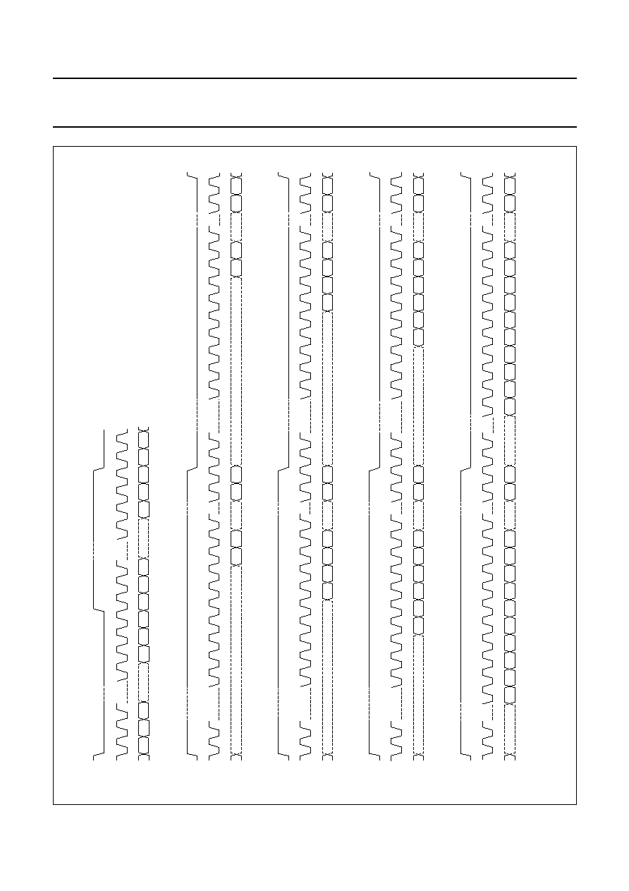
See Fig.3 for the general waveforms of the possible
formats.
When the applied word length exceeds 24 bits, the LSBs
are skipped.
The digital serial input/output circuitry is limited in handling
the number of BCK pulses per WS period. The maximum
allowed number of bit clocks per WS period is 256. Also
the number of bit clocks during WS LOW and HIGH must
be equal (50% WS duty factor) only for the LSB-justified
formats.
There are two modes in which the digital inputs can be
used (the mode is selectable via an I
2
C-bus bit):
∑
Use up to 4 digital serial inputs (8ch) with common WS
and BCK signal (8ch IN and 8ch OUT + 2ch FSDAC
output)
∑
Use one of the 2 SPDIF inputs as source instead of the
use of the digital serial inputs (2ch IN and
8ch OUT + One 2ch FSDAC output).
8.5.2
SPDIF
INPUTS
Two separate SPDIF receivers are available, one shared
with digital serial input 2 (SPDIF1) and one with the digital
serial input 3 (SPDIF2). The sample frequency at which
the SPDIF inputs can be used must be in the range of
32 to 96 kHz.
There are few control signals available from the SPDIF
input stage. These are connected to flags of the DSP:
∑
A lock signal indicating if the SPDIF input 1 or 2 is in
lock
∑
The pcm_audio/non-pcm_audio bit indicating if an audio
or data stream is detected on SPDIF input 1 or 2. The
FSDAC output will NOT be muted in the event of
non-audio PCM stream. This status bit can be read via
the I
2
C-bus, the microprocessor controller can decide to
put the DAC into MUTE (via pin POM).
Handling of channel status bits: The first 40 (of 192)
channel status bits of the selected SPDIF source (0FFBH,
bit 20), will come available in the I
2
C-bus registers
0FF2H to 0FF5H. Two registers 0FF2H to 0FF3H contain
the information for the right channel, the other two
(0FF4H to 0FF5H) contain the information for the left
channel. The information can be read via I
2
C-bus or by the
DSP program.
The design fulfils the digital audio interface specification
"IEC 60958-1 Ed2, part 1, general part IEC 60958-3 Ed2,
part 3, consumer applications".
2001
May
07
12
Philips Semiconductors
Preliminar
y specification
Digital Signal Processor
SAA7715H
This text is here in white to force landscape pages to be rotated correctly when browsing through the pdf in the Acrobat reader.This text is here in
_
white to force landscape pages to be rotated correctly when browsing through the pdf in the Acrobat reader.This text is here inThis text is here in
white to force landscape pages to be rotated correctly when browsing through the pdf in the Acrobat reader. white to force landscape pages to be ...
handbook, full pagewidth
MGR751
16
B5
B6
B7
B8
B9
B10
LEFT
LSB-JUSTIFIED FORMAT 24 BITS
WS
BCK
DATA
RIGHT
15
18
17
20
19
22
21
23
24
2
1
B3
B4
MSB
B2
B23
LSB
16
B5
B6
B7
B8
B9
B10
15
18
17
20
19
22
21
23
24
2
1
B3
B4
MSB
B2
B23
LSB
16
MSB
B2
B3
B4
B5
B6
LEFT
LSB-JUSTIFIED FORMAT 20 BITS
WS
BCK
DATA
RIGHT
15
18
17
20
19
2
1
B19
LSB
16
MSB
B2
B3
B4
B5
B6
15
18
17
20
19
2
1
B19
LSB
16
MSB
B2
B3
B4
LEFT
LSB-JUSTIFIED FORMAT 18 BITS
WS
BCK
DATA
RIGHT
15
18
17
2
1
MSB
B2
B3
B4
B17
LSB
16
15
18
17
2
1
B17
LSB
16
MSB
B2
LEFT
LSB-JUSTIFIED FORMAT 16 BITS
WS
BCK
DATA
RIGHT
15
2
1
B15
LSB
16
MSB
B2
15
2
1
B15
LSB
MSB
MSB
B2
2
1
>
= 8
1
2
3
LEFT
INPUT FORMAT I
2
S-BUS
WS
BCK
DATA
RIGHT
3
>
= 8
MSB
B2
Fig.3 All serial data input/output formats.

2001 May 07
13
Philips Semiconductors
Preliminary specification
Digital Signal Processor
SAA7715H
8.6
I
2
C-bus interface (pins SCL and SDA)
The I
2
C-bus format is described in
"The I
2
C-bus and how
to use it", order no. 9398 393 40011.
For the external control of the SAA7715 a fast I
2
C-bus is
implemented. This is a 400 kHz bus which is downward
compatible with the standard 100 kHz bus.
There are two different types of control instructions:
∑
Loading of the Program RAM (PRAM) with the required
DSP program
≠ Programming the coefficient RAM (YRAM)
≠ Instructions to control the DSP program.
∑
Selection of the digital serial input/output format to be
used, the DSP clock speed.
The detailed description of the I
2
C-bus and the description
of the different bits in the memory map is given in
Chapter 9.
8.7
Reset
The reset (pin DSP_RESET) is active LOW and needs an
external 22 k
pull-up resistor. Between this pin and the
V
SSI
ground a capacitor of 1
µ
F should be connected to
allow a proper switch-on of the supply voltage. The
capacitor value is such that the chip is in reset as long as
the power supply is not stabilized. A more or less fixed
relationship between the DSP reset and the POM time
constant is obligatory. The voltage on pin POM determines
the current flowing in the DACs.
The reset sets all I
2
C-bus bits to their default value and it
restarts the DSP program.
8.8
Power-down mode
The Power-down mode switches off all activity on the chip.
The Power-down mode can be switched on and off using
pin POWERDOWN. This pin needs to be connected to
ground if not used. The following applies for the
Power-down mode:
∑
Power-down mode may only be switched on when there
is no I
2
C-bus activity to or from the SAA7715
∑
Power-down mode may not be switched on before the
complete chip has been reset (DSP_RESET
active LOW)
∑
The clock signal on pin CLK_IN should be running
during Power-down mode
∑
It is advised to set pin POM to logic 0 before switching
on the Power-down mode and set it back to logic 1 after
the chip actually returns from Power-down mode as
shown in Fig.4
∑
All on-chip registers and memories will keep their values
during Power-down mode
∑
Digital serial outputs are not muted, the last value is kept
on the output
∑
The SAA7715 will not `lock-up' the I
2
C-bus during
Power-down mode (SDA line).
Figure 4 shows the time the chip actually is in Power-down
mode after switching on/off pin POWERDOWN.
handbook, full pagewidth
MGT828
tA
tB
POWERDOWN
device actually in
Power-down mode
POM
CLK_IN
Fig.4 Power-down mode.
t
A
= 4
◊
(256/CLK_IN); 8.192 MHz < CLK_IN < 12.288 MHz.
t
A
= 4
◊
(512/CLK_IN); 16.384 MHz < CLK_IN < 24.576 MHz.
t
B
= 128
◊
(256/CLK_IN); 8.192 MHz < CLK_IN < 12.288 MHz.
t
B
= 128
◊
(512/CLK_IN); 16.384 MHz < CLK_IN < 24.576 MHz.

2001 May 07
14
Philips Semiconductors
Preliminary specification
Digital Signal Processor
SAA7715H
8.9
Power supply connection and EMC
The digital part of the chip has in total 4 positive supply line
connections and 5 ground connections. To minimize
radiation the chip should be put on a double layer
printed-circuit board with on one side a large ground plane.
The ground supply lines should have a short connection to
this ground plane. A coil/capacitor network in the positive
supply line of the peripheral power supply line can be used
as high frequency filter. The core supply lines (V
DDI
) have
an on-chip decoupling capacitance, for EMC reasons an
external decoupling capacitance must not be used on this
pin. A series resistor plus capacitance is required for
proper operation on pin V
DDA2
, see Fig.11.
8.10
Test mode connections (pins TSCAN, RTCB
and SHTCB)
Pins TSCAN, RTCB and SHTCB are used to put the chip
in test mode and to test the internal connections. Each pin
has an internal pull-down resistor to ground. In the
application these pins can be left open or connected to
ground.
9
I
2
C-BUS PROTOCOL
9.1
Addressing
Before any data is transmitted on the I
2
C-bus, the device
that should respond is addressed first. The addressing is
always done with the first byte transmitted after the start
procedure.
9.2
Slave address (pin A0)
The SAA7715 acts as slave receiver or a slave transmitter.
Therefore the clock signal SCL is only an input signal. The
data signal SDA is a bidirectional line. The slave address
is shown in Table 6.
Table 6
Slave address
The sub-address bit A0 corresponds to the hardware
address pin A0 which allows the device to have 2 different
addresses. The A0 input is also used in test mode as serial
input of the test control block.
9.3
Write cycles
The I
2
C-bus configuration for a write cycle is shown
in Fig.5. The write cycle is used to write the bytes to the
DSP for manipulating the data and coefficients. More
details can be found in the I
2
C-bus memory map, see
Table 8.
The data length is 2, 3 or 4 bytes depending on the
accessed memory. If the Y-memory is addressed the data
length is 2 bytes, in the event of the X-memory the length
is 3 bytes. The slave receiver detects the address and
adjusts the number of bytes accordingly.
For this RAM-based product the internal P-memory
(PRAM) can be accessed via the I
2
C-bus interface. The
transmitted data-stream should be 4 bytes.
9.4
Read cycles
The I
2
C-bus configuration for a read cycle is shown
in Fig.6. The read cycle is used to read the data values
from XRAM, YRAM or PRAM. The master starts with a
START condition S, the SAA7715 address `0011110' and
a logic 0 (write) for the read/write bit. This is followed by an
acknowledge of the SAA7715. Then the master writes the
high memory address (ADDR H) and low memory address
(ADDR L) where the reading of the memory content of the
SAA7715 must start. The SAA7715 acknowledges these
addresses both.
The master generates a repeated START (Sr) and again
the SAA7715 address `0011110' but this time followed by
a logic 1 (read) of the read/write bit. From this moment on
the SAA7715 will send the memory content in groups of 3
(X/Y-memory or registers) or 4 (P-memory) bytes to the
I
2
C-bus each time acknowledged by the master. The
master stops this cycle by generating a negative
acknowledge, then the SAA7715 frees the I
2
C-bus and the
master can generate a STOP condition.
The data is transferred from the DSP register to the
I
2
C-bus register at execution of the MPI instruction in the
DSP program. Therefore at least once every DSP routine
an MPI instruction should be added.
MSB
LSB
0
0
1
1
1
1
A0
R/W

2001
May
07
15
Philips Semiconductors
Preliminar
y specification
Digital Signal Processor
SAA7715H
This text is here in white to force landscape pages to be rotated correctly when browsing through the pdf in the Acrobat reader.This text is here in
_
white to force landscape pages to be rotated correctly when browsing through the pdf in the Acrobat reader.This text is here inThis text is here in
white to force landscape pages to be rotated correctly when browsing through the pdf in the Acrobat reader. white to force landscape pages to be ...
0 1 1 1 1 0 0
A
C
K
A
C
K
A
C
K
A
C
K
A
C
K
address
S
0
ADDR H
ADDR L
DATA 1
DATA ...
R/W
MGU331
auto increment if repeated n-groups of 2, 3 or 4 bytes
P
A
C
K
DATA 4
Fig.5 Master transmitter writes to the SAA7715 registers.
S = START condition.
P = STOP condition.
ACK = acknowledge from SAA7715.
ADDR H and ADDR L = address DSP register.
DATA 1 to DATA 4 = 2, 3 or 4 bytes data word.
0 1 1 1 1 0 0
A
C
K
A
C
K
A
C
K
A
C
K
A
C
K
address
S
0
0 1 1
1
1 1 0
S
r
0
ADDR H
ADDR L
DATA 1
R/W
MGU330
auto increment if repeated n-groups of 2, 3 or 4 bytes
R
A
C
K
P
N
A
A
C
K
DATA ...
DATA 4
R/W
Fig.6 Master transmitter reads from the SAA7715 registers.
S = START condition.
Sr = repeated START condition.
P = STOP condition.
ACK = acknowledge from SAA7715 (SDA LOW).
R = repeat n-times the 2, 3 or 4 bytes data group.
NA = Negative Acknowledge master (SDA HIGH).
ADDR H and ADDR L = address DSP register.
DATA 1 to DATA 4 = 2, 3 or 4 bytes data word.

2001 May 07
16
Philips Semiconductors
Preliminary specification
Digital Signal Processor
SAA7715H
9.5
Program RAM
The SAA7715 has a 1.5 kbyte PRAM to store the DSP
instruction code into. Also a 2 kbyte PROM is on-chip
available and can be accessed (memory mapped) without
the need of selecting the PROM or PRAM. The DSP
instruction code can be downloaded into the PRAM via the
I
2
C-bus. The write and read cycle are shown in Figs 5
and 6 respectively.
The DSP has an instruction word width of 32 bits which
means that this space should be accessed with 4 bytes in
consecutive order and does have the auto-increment
function.
9.6
Data word alignment
It is possible to transfer data via the I
2
C-bus to a
destination where it can have different data word length.
Those destinations with data word are shown in Table 7.
Table 7
Data word alignment
SOURCE
DESTINATION
DATA WORD
BYTES
(NUMBER)
I
2
C-bus
DSP-PRAM
MBBB BBBB BBBB BBBB BBBB BBBB BBBB BBBL
4
I
2
C-bus
DSP and general control
MBBB BBBB BBBB BBBB BBBB BBBL
3
I
2
C-bus
I
2
C-bus registers
MBBB BBBB BBBB BBBB BBBB BBBL
3
I
2
C-bus
DSP-XRAM
MBBB BBBB BBBB BBBB BBBB BBBL
3
I
2
C-bus
DSP-YRAM
XXXX MBBB BBBB BBBL
2

2001 May 07
17
Philips Semiconductors
Preliminary specification
Digital Signal Processor
SAA7715H
9.7
I
2
C-bus memory map specification
The I
2
C-bus memory map contains all defined I
2
C-bus bits. The map is split up in two different sections: the hardware
memory registers and the RAM definitions. In Table 8 the preliminary memory map is depicted. The hardware registers
are memory map on the XRAM of DSP. Table 9 shows the detailed memory map of those locations. All locations are
acknowledged by the SAA7715 even if the user tries to write to a reserved space. The data in these sections will be lost.
Reading from these locations will result in undefined data words.
Table 8
I
2
C-bus memory map
Table 9
I
2
C-bus memory map overview
ADDRESS
FUNCTION
SIZE
8000H to 87FFH
DSP to PROM (not readable via
I
2
C-bus)
2k
◊
32 bits
602FH
DSP and general control
1
◊
24 bits
2000H to 25FFH
DSP to PRAM
1.5k
◊
32 bits
1000H to 01FFH
DSP to YRAM
512
◊
12 bits
0FF2H to 0FF5H, 0FFBH
I
2
C-bus register
1
◊
24 bits
0000H to 09FFH
DSP to XRAM
2.5k
◊
24 bits
ADDRESS
DESCRIPTION
Hardware registers
0FFBH
Selector register 1
0FF5H
SPDIF IN channel status register 1 left
0FF4H
SPDIF IN channel status register 2 left
0FF3H
SPDIF IN channel status register 1 right
0FF2H
SPDIF IN channel status register 2 right
DSP control
602FH
DSP and general control register
2001 May 07
18
Philips Semiconductors
Preliminary specification
Digital Signal Processor
SAA7715H
9.8
I
2
C-bus memory map definition
Table 10 DSP and general control register (602FH)
Table 11 SPDIF IN channel status register 2 right (0FF2H)
Table 12 SPDIF IN channel status register 1 right (0FF3H)
NAME
SIZE
(BITS)
DESCRIPTION
DEFAULT
BIT
POSITION
1
reserved
0
0
pll_div[4:0]
5
PLL clock division factor according to Table 2
00011
5 to 1
dsp_turbo
1
PLL output frequency
1
6
1: double
0: no doubling
1
reserved
1
7
pc_reset_dsp
1
program counter reset DSP
0
8
1: reset on
0: reset off
2
reserved
00
10 to 9
sel[2:0]
3
selection of n
◊
f
s
clock at SYSCLK output according to
Table 4
010
13 to 11
sel_loop_div[1:0]
2
word select input range selection for WS_PLL according
to Table 3
01
15 to 14
2
reserved
00
17 to 16
sel_FSDAC_clk
2
clock source for FSDAC
00
19 to 18
00: WS_PLL if no signal to pin CLK_IN
01: 512f
s
to pin CLK_IN
11: 256f
s
to pin CLK_IN
dis_SYSCLK
1
output on pin SYSCLK
0
20
1: disable
0: enable
256f
s
_n*Fs
1
signal on pin SYSCLK
0
21
1: fixed 256f
s
clock
0: n
◊
f
s
clock; determined by bits 13 to 11
1
reserved
0
23 to 22
NAME
SIZE
(BITS)
DESCRIPTION
DEFAULT
BIT
POSITION
ch_stat_in right lsb
20
channel status SPDIF in right LSB bits 19 to 0
00000H
19 to 0
NAME
SIZE
(BITS)
DESCRIPTION
DEFAULT
BIT
POSITION
ch_stat_in right msb
20
channel status SPDIF in right MSB bits 39 to 20
00000H
19 to 0

2001 May 07
19
Philips Semiconductors
Preliminary specification
Digital Signal Processor
SAA7715H
Table 13 SPDIF IN channel status register 2 left (0FF4H)
Table 14 SPDIF IN channel status register 1 left (0FF5H)
Table 15 Selector register 1 (0FFBH)
NAME
SIZE
(BITS)
DESCRIPTION
DEFAULT
BIT
POSITION
ch_stat_in left lsb
20
channel status SPDIF in2 left LSB bits 19 to 0
00000H
19 to 0
NAME
SIZE
(BITS)
DESCRIPTION
DEFAULT
BIT
POSITION
ch_stat_in left msb
20
channel status SPDIF in2 left MSB bits 39 to 20
00000H
19 to 0
NAME
SIZE
(BITS)
DESCRIPTION
DEFAULT
BIT
POSITION
format_in1
3
digital serial inputs 1 and 4 data format according to
Table 17
011
2 to 0
format_in2
3
digital serial input 2 data format according to Table 17
011
5 to 3
format_in3
3
digital serial input 3 data format according to Table 17
011
8 to 6
format_out
3
digital serial outputs 1 to 4 data format according to
Table 18
000
11 to 9
en_output
1
enable or disable digital serial outputs
1
12
1: enable
0: disable
1
reserved
0
13
master_source
4
source selection
0000
14 to 17
0000: digital serial input 1
0101: digital serial input 2 or SPDIF 1 (see bit 18)
1010: digital serial input 3 or SPDIF 2 (see bit 19)
all other values are reserved
spdif_sel1
1
SPDIF1 or digital serial input 2
0
18
1: SPDIF1
0: digital serial input 2
spdif_sel2
1
SPDIF2 or digital serial input 3
0
19
1: SPDIF2
0: digital serial input 3
sel_spdifin_chstat
1
select channel status information taken from SPDIF1 or
SPDIF2
0
20
1: from input SPDIF2
0: from input SPDIF1
3
reserved
000
21 to 23

2001 May 07
20
Philips Semiconductors
Preliminary specification
Digital Signal Processor
SAA7715H
Table 16 Default settings of I
2
C-bus registers after power-up and reset
9.9
Table definitions
Table 17 Digital serial format for inputs 1 to 4
Table 18 Digital serial formats for outputs 1 to 4
I
2
C-BUS ADDRESS
DEFAULT VALUE
602FH
0050C6H
0FFBH
0010DBH
0FF5H
000000H
0FF4H
000000H
0FF3H
000000H
0FF2H
000000H
FORMAT_IN 1, 2 AND 3
OUTPUT
BIT 2
BIT 1
BIT 0
0
1
1
standard I
2
S-bus
1
0
0
LSB-justified, 16 bits
1
0
1
LSB-justified, 18 bits
1
1
0
LSB-justified, 20 bits
1
1
1
LSB-justified, 24 bits
FORMAT_OUT
OUTPUT
BIT 2
BIT 1
BIT 0
0
0
0
standard I
2
S-bus
1
0
0
LSB-justified, 16 bits
1
0
1
LSB-justified, 18 bits
1
1
0
LSB-justified, 20 bits
1
1
1
LSB-justified, 24 bits
10 SOFTWARE IN ROM DESCRIPTION
10.1
Audio dynamics compressor
10.1.1
T
HEORY OF OPERATION
The objective of a dynamics compressor is to reduce the
dynamic range of the input signal for purposes of
accommodating downstream devices, or simply to give the
audio signal a different character. Early compressors were
used primarily for limiting signals destined for recording on
media with limited dynamic range. In the present day,
compressors are routinely used in recording studios and in
live performances to enhance the presence of various
signals.
The behaviour of a dynamics compressor is very similar to
that of an Automatic Gain Control (AGC), the central idea
being to scale the input signal by a slowly varying gain
factor that is in turn regulated by the level of the input
signal. The essential concepts are summed up nicely by
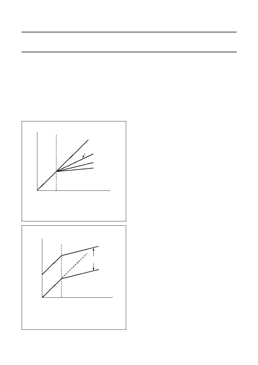
Fig.7. Here we observe that when the input level exceeds
a selected threshold, gain reduction is brought to bear
according to the selected compression ratio, while signals
appearing below the threshold are passed with unity gain.
The net effect, therefore, is to compress the louder
passages of source material.
2001 May 07
21
Philips Semiconductors
Preliminary specification
Digital Signal Processor
SAA7715H
Ironically, most people think in terms of boosting the low
signals when talking about dynamics compression. In fact,
this is what actually happens after the output is rescaled to
account for the gain reduction imposed by the current
settings. By doing this the output signal can be forced to
carry more power than the input. This is what gives the
compressor its `punch' quality, for a more `in your face' sort
of sound. Figure 8 shows an example of the transfer
curves before and after application of output gain. Users
should be aware, however, that abuse of output gain can
amplify system noise to intolerable levels.
10.1.1.1
Control parameters
Common to most compressors are five control parameters
used for adjusting the behaviour of the compressor. These
are typically labelled as threshold, ratio, attack time,
release time, and output. By careful adjustment of these
controls a skilled user can produce very pleasing results
for a wide variety input source material. In the following
subsections, functionality of each control is described.
10.1.1.2
Fixed versus variable mode
The compressor module can be operated in so-called
`fixed' mode or `variable' mode. When in variable mode,
the user has full control over both the threshold and ratio
controls. In fixed mode, controls are frozen and the effect
operates at a fixed ratio of 2:1, with a threshold setting of
-
36 dB(FS). These settings were chosen as a good
compromise for a wide variety of source material.
10.1.1.3
Threshold
Threshold determines the level at which gain reduction
begins. For example, if the threshold is set at
-
10 dB(FS),
this means that all signals below
-
10 dB(FS) will be
passed unaltered. Only when the input level exceeds this
threshold is gain reduction (compression) brought to bear.
Many times a dramatic change in the threshold setting will
call for a ratio adjustment. Experiment with these two
controls to find what works best for your system, your
music, and most importantly, your ears.
10.1.1.4
Ratio
The ratio control sets the desired compression ratio.
Settings are traditionally expressed in ratios such as 1.5:1,
2:1, 4:1, 10:1, etc. An explanation of how to interpret these
settings is best served by example. Say we are dealing
with a ratio of 1.5:1. This means that for every 1.5 dB
increase in input level beyond the threshold, only 1 dB is
passed to the output. Another way of explaining this is in
terms of gain reduction. In this particular case a 0.5 dB
gain reduction is imposed for every 1.5 dB increase
beyond the threshold level.
Compression ratio is changed by selecting one of the
values in the drop-down list labelled `Ratio'. To increase
the amount of compression, select one of the higher ratios.
For a more subtle effect, select a lower setting, such as
1.5:1.
handbook, halfpage
threshold
no compression
2:1 compression
4:1 compression
10:1 compression
(limiting)
slope =
1/2
output
level
(dB)
input level (dB)
MGT829
Fig.7
Gain reduction is applied only when the
signal exceeds the set threshold level.
handbook, halfpage
threshold
4:1 compression
output
gain
output
level
(dB)
input level (dB)
MGT830
Fig.8
Output gain can be used to restore the peak
level to its maximum.

2001 May 07
22
Philips Semiconductors
Preliminary specification
Digital Signal Processor
SAA7715H
10.1.1.5
Attack time
Attack time controls the rate at which gain-reduction is
engaged following the detection of the input signal
exceeding the threshold level. Typical values are in the
range of 0 to 100 ms. Fast attack times tend to smooth out
abrupt transients thereby helping to ensure the output
level remains fairly consistent; however, at the same time
fast attack times can easily destroy much of the dynamic
character of sources having very distinguished attack
transients (such as a piano or an acoustic guitar). Slow
attack times, on the other hand, allow the sources attack
transients to pass through virtually unaltered, thereby
retaining most of the dynamic signature of the source. The
danger here, however, is the possibility of clipping the
output, or overloading one or more downstream
components.
The present implementation of the compressor does not
provide user access to attack time.
10.1.1.6
Release time
Complementing the attack time control, release time
controls the speed at which the compressor disengages
after the input level falls back below the threshold. Typical
values here range from around 100 ms to several
seconds.
The present implementation of the compressor does not
provide user access to release time.
10.1.1.7
Output or `make-up gain'
In order to make maximum use of the available bit
resolution, it becomes necessary to boost the
compressors output in order to ensure the signal swings
close to the maximum excursions allowed by the digital
output. Notice in Fig.7 how the output level can be
dramatically reduced, particularly at low threshold levels
and high compression ratios. In the present
implementation, this rescaling is managed automatically
according to the current threshold and ratio settings.
10.2
Audio enhancer
10.2.1
T
HEORY OF OPERATION
The enhancer uses non-linear processing to generate
extra harmonics, which are added to the audio to improve
high frequency detail. It is particularly useful with
streaming audio from the Internet, which is typically
compressed to the extent that the original high frequency
content is lost.
The enhancer is also a very effective means of improving
the sound of CD-quality audio, by restoring the presence
and brilliance of the original acoustic performance.
10.2.1.1
Control parameters
The enhancer has a single mix control, which determines
the amount of generated harmonics to be added to the
signal. High settings will result in a brighter effect with
greater depth. For particularly dull audio, such as is often
received over the Internet, a high mix level will have a
pleasing effect. Intermediate settings are appropriate for
CD-quality audio, although classical music listeners may
prefer to use the enhancer sparingly.
10.3
Equalizer
10.3.1
G
ENERAL DESCRIPTION
∑
2-channels
∑
5-bands
∑
Control range: 20 Hz to 20 kHz.
10.3.2
O
VERVIEW
The fundamental ideal for any high-fidelity audio rendering
system is to reproduce the aural experience present at the
time and place the original audio material was recorded.
Unfortunately, practically all systems fall short of this ideal
to some degree for a number of reasons. While
environmental acoustics can play a significant role, in
many cases performance deficiencies associated with the
loudspeakers cause most of the `distortion'. This happens
when the loudspeakers cannot deliver a uniform frequency
response over the entire audio range (20 Hz to 20 kHz).
Equalizers were invented to deal with frequency response
problems by boosting or cutting selected frequency bands
in the signal. Used in the right manner, a properly adjusted
equalizer can effectively compensate for loudspeaker
performance deficiencies, or any other frequency
dependent amplitude variations in the system.
Additionally, equalization can be used to create a
customized frequency response which is better suited for
a particular listener or a particular style of music, for
instance.
The type of equalizer provided with this system is of the
parametric variety. Parametric equalizers differ from
graphic equalizers by giving the user more control over the
filters that actually effect the boost or cut of a particular
band. More specifically, for each band, users can control
the band's centre frequency, and also the width of the
band of frequencies that are affected.

2001 May 07
23
Philips Semiconductors
Preliminary specification
Digital Signal Processor
SAA7715H
10.3.3
C
ONTROLS
The equalizer module exposes three controls for each of
the five bands. These are referred to as gain, centre
frequency, and Q. The gain control sets the amount of
boost or cut applied to the particular band of frequencies.
Centre frequency controls the frequency at which the
boost or cut filter is centred, while the Q control determines
the bandwidth (the range of frequencies) over which the
filter operates.
10.3.4
C
ENTRE FREQUENCY
Centre frequency defines the frequency where boost or cut
will be centred. To set the centre frequency, select the
entry box and type in a number that is within the allowed
range.
10.3.5
G
AIN
Use the gain control to adjust the amount or boost or cut.
Move the slider upward (above the 0 dB line) to add boost,
downward (below the 0 dB line) to cut.
10.3.6
Q
The Q parameter determines the sharpness of the filter.
As the value of Q increases, the filter becomes narrower,
thereby reducing the filters effective bandwidth. High Q
filters are useful for reducing speaker resonances, or for
eliminating resonance that may be caused by the acoustic
environment. Low Q filters, on the other hand, are useful
for operating on a broad range of frequencies.
10.3.7
H
INTS AND TIPS
Avoid using the equalizer for volume control. This is not the
purpose of an equalizer. Remember, you are only trying to
correct frequency response deviations from some `ideal'
response that are due to loudspeaker deficiencies and
perhaps the surrounding environment. Therefore you
should strive to introduce the minimum amount of
equalization that causes the system output to reach your
desired response.
Avoid excessive boost or cut. This can introduce
noticeable coloration of the program material.
10.4
Stereo spatializer
10.4.1
O
VERVIEW
In PC listening settings, the quality of the stereo image is
sometimes compromised by the short distance between
the loudspeakers, and also by the physical limitations of
the loudspeakers themselves. The spatializer effect
remedies these shortcomings by applying perceptually
tuned signal-processing to create the illusion of a wider
and more enveloping sound stage.
Users should be relieved to know that relative positioning
of instruments in the original material is preserved. In other
words, tracks that are centre mixed in the original material
remain centred; tracks panned left or right in the original
mix remain left and right panned. The main difference is in
the apparent width and depth of the sound stage, it is as
though the listener is hearing a larger and more distant pair
of speakers, spaced much farther apart than those actually
present.
10.4.2
C
ONTROLS
The spatializer effect uses only one control to change its
behaviour.
10.4.3
M
IX
The mix control sets the intensity of the effect. Control is
straight-forward. Add more effect by pulling the slider
upward; move the slider downward to reduce the amount
of effect.
10.4.4
H
INTS AND TIPS
Try a mix setting of about 0.7 as a starting point.
For best results, position yourself between the speakers
and a couple of feet back. Ideally, your ears should be at
about the same level as the speakers, but this is not so
critical.

2001 May 07
24
Philips Semiconductors
Preliminary specification
Digital Signal Processor
SAA7715H
11 LIMITING VALUES
In accordance with the Absolute Maximum Ratings System (IEC 60134).
Notes
1. Machine model (R = 0
; C = 100 pF; L = 2.5
µ
H).
2. Human body model (R = 1500
; C = 100 pF).
12 THERMAL CHARACTERISTICS
SYMBOL
PARAMETER
CONDITIONS
MIN.
MAX.
UNIT
V
DD
supply voltage
-
0.5
+3.6
V
V
I
input voltage
-
0.5
+5.5
V
I
IK
input clamping diode current
V
I
<
-
0.5 V or V
I
> V
DD
+ 0.5 V
-
±
10
mA
I
OK
output clamping diode current
V
O
<
-
0.5 V or V
O
> V
DD
+ 0.5 V
-
±
20
mA
I
O(sink/source)
output source or sink current
-
0.5 V < V
O
< V
DD
+ 0.5 V
-
±
20
mA
I
DD
,I
SS
V
DD
or V
SS
current per supply pin
-
±
50
mA
T
amb
ambient temperature
-
40
+85
∞
C
T
stg
storage temperature
-
65
+125
∞
C
V
ESD
electrostatic handling voltage
note 1
200
-
V
note 2
2000
-
V
I
lu(prot)
latch-up protection current
CIC specification/test method
100
-
mA
P
tot
total power dissipation
-
600
mW
SYMBOL
PARAMETER
CONDITIONS
VALUE
UNIT
R
th(j-a)
thermal resistance from junction to ambient
mounted on printed-circuit
board
60
K/W

2001 May 07
25
Philips Semiconductors
Preliminary specification
Digital Signal Processor
SAA7715H
13 CHARACTERISTICS
V
DD
= 3.15 to 3.45 V; unless otherwise specified.
SYMBOL
PARAMETER
CONDITIONS
MIN.
TYP.
MAX.
UNIT
Supplies; T
amb
=
-
40 to +85
∞
C
V
DD
operating supply voltage
all pins V
DD
with
respect to pins V
SS
3.15
3.3
3.45
V
I
DDD
supply current of the digital part
-
95
-
mA
I
DDD(core)
supply current of the digital core
part
high activity of the
DSP at DSPFREQ
frequency
-
90
-
mA
I
DDD(peri)
supply current of the digital
periphery part
no external load to
ground
-
5
-
mA
I
DDA
supply current of the analog part
zero input and output
signal
-
20
-
mA
I
DDA(DAC)
supply current of the DAC
zero input and output
signal
-
6.5
13
mA
Power-down mode
-
250
-
µ
A
I
DDA(SPDIF)
supply current of the SPDIF
inputs, on-chip PLL and WSPLL
zero input and output
signals
-
13.5
27
mA
P
tot
total power dissipation
-
380
-
mW
I
POWERDOWN
DC supply current of the total chip
in Power-down mode
pin POWERDOWN
enabled
-
400
-
µ
A
Digital I/O; T
amb
=
-
40 to +85
∞
C; V
DD
= 3.15 to 3.45 V; unless otherwise specified
V
IH
HIGH-level input voltage all digital
inputs and I/Os
2.0
-
-
V
V
IL
LOW-level input voltage all digital
inputs and I/Os
-
-
0.8
V
V
hys
Schmitt-trigger hysteresis
0.4
-
-
V
V
OH
HIGH-level output voltage
standard output;
I
O
=
-
4 mA
V
DD
-
0.4
-
-
V
5 ns slew rate output;
I
O
=
-
4 mA
V
DD
-
0.4
-
-
V
10 ns slew rate
output; I
O
=
-
2 mA
V
DD
-
0.4
-
-
V
20 ns slew rate
output; I
O
=
-
1 mA
V
DD
-
0.4
-
-
V
2001 May 07
26
Philips Semiconductors
Preliminary specification
Digital Signal Processor
SAA7715H
V
OL
LOW-level output voltage
standard output;
I
O
= 4 mA
-
-
0.4
V
5 ns slew rate output;
I
O
= 4 mA
-
-
0.4
V
10 ns slew rate
output; I
O
= 2 mA
-
-
0.4
V
20 ns slew rate
output; I
O
= 1 mA
-
-
0.4
V
I
2
C-bus output;
I
O
= 4 mA
-
-
0.4
V
I
LO
output leakage current 3-state
outputs
V
O
= 0 V or V
DD
-
-
±
5
µ
A
R
pd
internal pull-down resistor to V
SS
24
50
140
k
R
pu
internal pull-up resistor to V
DD
30
50
100
k
C
i
input capacitance
-
-
3.5
pF
t
i(r)
,t
i(f)
input rise and fall times
V
DD
= 3.45 V
-
6
200
ns
t
o(t)
output transition time
standard output;
C
L
= 30 pF
-
3.5
-
ns
5 ns slew rate output;
C
L
= 30 pF
-
5
-
ns
10 ns slew rate
output; C
L
= 30 pF
-
10
-
ns
20 ns slew rate
output; C
L
= 30 pF
-
20
-
ns
I
2
C-bus output;
C
L
= 400 pF
60
-
300
ns
AC characteristics SPDIF1 and SPDIF2 inputs; T
amb
= 25
∞
C; V
DDA2
= 3.3 V; unless otherwise specified
V
i(p-p)
AC input level (peak-to-peak level)
0.2
0.5
3.3
V
R
i
input impedance
at 1 kHz
-
6
-
k
V
hys
hysteresis of input voltage
-
40
-
mV
SYMBOL
PARAMETER
CONDITIONS
MIN.
TYP.
MAX.
UNIT
2001 May 07
27
Philips Semiconductors
Preliminary specification
Digital Signal Processor
SAA7715H
Analog DAC outputs; V
DDA1
= 3.3 V; f
s
= 44.1 kHz; T
amb
= 25
∞
C; R
L
= 5 k
; all voltages referenced to ground;
unless otherwise specified
DC
CHARACTERISTICS
R
o(DAC)
DAC output resistance
pins 34 and 36
-
0.13
3.0
I
o(max)
maximum output current
(THD + N)/S < 0.1%
R
L
= 5 k
-
0.22
-
mA
R
L
load resistance
3
-
-
k
C
L
load capacitance
-
-
200
pF
R
o(VREFDA)
VREFDA output resistance
pin 38
-
28
-
k
AC
CHARACTERISTICS
V
o(rms)
output voltage (RMS value)
-
1000
-
mV
V
o
unbalance between channels
-
0.1
-
dB
(THD + N)/S
total harmonic distortion plus
noise-to-signal ratio
at 0 dB
-
-
85
-
dB(A)
at
-
60 dB
-
-
37
-
dB(A)
S/N
signal-to-noise ratio
code = 0
-
100
-
dB(A)
cs
channel separation
-
80
-
dB
PSRR
power supply rejection ratio
f
ripple
= 1 kHz;
V
ripple(p-p)
= 1%
-
50
-
dB
SYMBOL
PARAMETER
CONDITIONS
MIN.
TYP.
MAX.
UNIT

2001 May 07
28
Philips Semiconductors
Preliminary specification
Digital Signal Processor
SAA7715H
14 I
2
S-BUS TIMING
handbook, full pagewidth
WS
BCK
DATA IN
RIGHT
LSB
MSB
LEFT
tsu(WS)
th(WS)
tsu(D)
th(D)
tBCK(H)
td(D)
tBCK(L)
Tcy
tr
tf
MGM129
DATA OUT
LSB
MSB
Fig.9 Timing of the digital audio data inputs and outputs.
Table 19 Timing digital serial audio inputs and outputs (see Fig.9)
SYMBOL
PARAMETER
CONDITIONS
MIN.
TYP.
MAX.
UNIT
T
cy
bit clock cycle time
162
-
-
ns
t
r
rise time
T
cy
= 50 ns
-
-
0.15T
cy
ns
t
f
fall time
T
cy
= 50 ns
-
-
0.15T
cy
ns
t
BCK(H)
bit clock HIGH time
T
cy
= 50 ns
0.35T
cy
-
-
ns
t
BCK(L)
bit clock LOW time
T
cy
= 50 ns
0.35T
cy
-
-
ns
t
su(D)
data set-up time
T
cy
= 50 ns
0.2T
cy
-
-
ns
t
h(D)
data hold time
T
cy
= 50 ns
0.2T
cy
-
-
ns
t
d(D)
data delay time
T
cy
= 50 ns
-
-
0.15T
cy
ns
t
su(WS)
word select set-up time
T
cy
= 50 ns
0.2T
cy
-
-
ns
t
h(WS)
word select hold time
T
cy
= 50 ns
0.2T
cy
-
-
ns
2001 May 07
29
Philips Semiconductors
Preliminary specification
Digital Signal Processor
SAA7715H
15 I
2
C-BUS TIMING
handbook, full pagewidth
MSC610
S
Sr
tSU;STO
tSU;STA
tHD;STA
tHIGH
tLOW
tSU;DAT
tHD;DAT
tf
SDA
SCL
P
S
tBUF
tr
tf
tr
tSP
tHD;STA
Fig.10 Definition of timing on the I
2
C-bus.
Table 20 Timing of I
2
C-bus (see Fig.10)
SYMBOL
PARAMETER
CONDITIONS
STANDARD MODE
I
2
C-BUS
FAST MODE I
2
C-BUS
UNIT
MIN.
MAX.
MIN.
MAX.
f
SCL
SCL clock frequency
0
100
0
400
kHz
t
BUF
bus free time between a
STOP and START
condition
4.7
-
1.3
-
µ
s
t
HD;STA
hold time (repeated)
START condition; after this
period, the first clock pulse
is generated
4.0
-
0.6
-
µ
s
t
LOW
SCL LOW period
4.7
-
1.3
-
µ
s
t
HIGH
SCL HIGH period
4.0
-
0.6
-
µ
s
t
SU;STA
set-up time for a repeated
START condition
4.7
-
0.6
-
µ
s
t
HD;DAT
DATA hold time
0
-
0
0.9
µ
s
t
SU;DAT
DATA set-up time
250
-
100
-
ns
t
r
rise time of both SDA and
SCL signals
C
b
in pF
-
1000
20 + 0.1C
b
300
ns
t
f
fall time of both SDA and
SCL signals
C
b
in pF
-
300
20 + 0.1C
b
300
ns
t
SU;STO
set-up time for STOP
condition
4.0
-
0.6
-
µ
s
C
b
capacitive load for each
bus line
-
400
-
400
pF
t
SP
pulse width of spikes to be
suppressed by input filter
not applicable
0
50
ns

2001
May
07
30
Philips Semiconductors
Preliminar
y specification
Digital Signal Processor
SAA7715H
This text is here in white to force landscape pages to be rotated correctly when browsing through the pdf in the Acrobat reader.This text is here in
_
white to force landscape pages to be rotated correctly when browsing through the pdf in the Acrobat reader.This text is here inThis text is here in
white to force landscape pages to be rotated correctly when browsing through the pdf in the Acrobat reader. white to force landscape pages to be ...
16
APPLICA
TION DIA
GRAM
a
ndbook, full pagewidth
MGT831
4.7 k
4.7 k
22 k
100
100
10 k
10 k
22 k
47
µ
F
47
µ
F
47
µ
F
1
µ
F
(1)
100 nF
100
nF
100
nF
100
nF
4.7
µ
F
+
5 V
+
5 V
+
3.3 V
+
3.3 V
SAA7715H
TCB
PRAM
PROM
DSP CORE
STEREO
DAC
256 fs
CLOCK
I
2
C-BUS
WS_PLL
I
2
C-bus
˜
2
PLL
1
IIS_BCK1
2
24
25
IIS_WS1
3
IIS_IN1
5
IIS_IN4
IIS_OUT1
31
IIS_OUT2
30
IIS_OUT3
29
IIS_OUT4
28
VOUTL
34
VOUTR
36
IIS_BCK
33
IIS_WS
32
POM
39
VREFDA
38
digital
inputs
digital
outputs
9
22
41
IIS_IN3
CLK_IN
DIV_CLK_IN
6
DSP CLOCK
DSP flags
microcontroller
microcontroller
microcontroller
right output
left output
IIS_IN2
S
XRAM
YRAM
L1
L2
44
DSP_INOUT7
43
DSP_INOUT6
42
DSP_INOUT5
20
SHTCB
19
RTCB
V
SSI2
26
TSCAN
27
10
V
SSI1
14
V
SSE
21
V
SSA2
15
V
DDI1
16
V
DDE
23
V
DDA2
17
V
DDA1
SPDIF2
SPDIF1
35
V
SSA1
37
SYSCLK
18
DSP_RESET
13
SDA
12
SCL
11
A0
40
POWERDOWN
10
10
75
47
µ
F
47
µ
F
47
µ
F
100 nF
SPDIF
input signals
100 nF
100 pF
75
100 pF
4
RESERVED1
7
RESERVED2
8
RESERVED3
Fig.11 Application diagram.
(1) Omit this capacitor when a microcontroller is used.

2001 May 07
31
Philips Semiconductors
Preliminary specification
Digital Signal Processor
SAA7715H
17 PACKAGE OUTLINE
UNIT
A
1
A
2
A
3
b
p
c
E
(1)
e
H
E
L
L
p
Z
y
w
v
REFERENCES
OUTLINE
VERSION
EUROPEAN
PROJECTION
ISSUE DATE
IEC
JEDEC
EIAJ
mm
0.25
0.05
1.85
1.65
0.25
0.40
0.20
0.25
0.14
10.1
9.9
0.8
1.3
12.9
12.3
1.2
0.8
10
0
o
o
0.15
0.1
0.15
DIMENSIONS (mm are the original dimensions)
Note
1. Plastic or metal protrusions of 0.25 mm maximum per side are not included.
0.95
0.55
SOT307-2
95-02-04
97-08-01
D
(1)
(1)
(1)
10.1
9.9
H
D
12.9
12.3
E
Z
1.2
0.8
D
e
E
B
11
c
E
H
D
ZD
A
Z E
e
v
M
A
X
1
44
34
33
23
22
12
y
A
1
A
L
p
detail X
L
(A )
3
A
2
pin 1 index
D
H
v
M
B
b
p
b
p
w
M
w
M
0
2.5
5 mm
scale
QFP44: plastic quad flat package; 44 leads (lead length 1.3 mm); body 10 x 10 x 1.75 mm
SOT307-2
A
max.
2.10

2001 May 07
32
Philips Semiconductors
Preliminary specification
Digital Signal Processor
SAA7715H
18 SOLDERING
18.1
Introduction to soldering surface mount
packages
This text gives a very brief insight to a complex technology.
A more in-depth account of soldering ICs can be found in
our
"Data Handbook IC26; Integrated Circuit Packages"
(document order number 9398 652 90011).
There is no soldering method that is ideal for all surface
mount IC packages. Wave soldering can still be used for
certain surface mount ICs, but it is not suitable for fine pitch
SMDs. In these situations reflow soldering is
recommended.
18.2
Reflow soldering
Reflow soldering requires solder paste (a suspension of
fine solder particles, flux and binding agent) to be applied
to the printed-circuit board by screen printing, stencilling or
pressure-syringe dispensing before package placement.
Several methods exist for reflowing; for example,
convection or convection/infrared heating in a conveyor
type oven. Throughput times (preheating, soldering and
cooling) vary between 100 and 200 seconds depending
on heating method.
Typical reflow peak temperatures range from
215 to 250
∞
C. The top-surface temperature of the
packages should preferable be kept below 220
∞
C for
thick/large packages, and below 235
∞
C for small/thin
packages.
18.3
Wave soldering
Conventional single wave soldering is not recommended
for surface mount devices (SMDs) or printed-circuit boards
with a high component density, as solder bridging and
non-wetting can present major problems.
To overcome these problems the double-wave soldering
method was specifically developed.
If wave soldering is used the following conditions must be
observed for optimal results:
∑
Use a double-wave soldering method comprising a
turbulent wave with high upward pressure followed by a
smooth laminar wave.
∑
For packages with leads on two sides and a pitch (e):
≠ larger than or equal to 1.27 mm, the footprint
longitudinal axis is preferred to be parallel to the
transport direction of the printed-circuit board;
≠ smaller than 1.27 mm, the footprint longitudinal axis
must be parallel to the transport direction of the
printed-circuit board.
The footprint must incorporate solder thieves at the
downstream end.
∑
For packages with leads on four sides, the footprint must
be placed at a 45
∞
angle to the transport direction of the
printed-circuit board. The footprint must incorporate
solder thieves downstream and at the side corners.
During placement and before soldering, the package must
be fixed with a droplet of adhesive. The adhesive can be
applied by screen printing, pin transfer or syringe
dispensing. The package can be soldered after the
adhesive is cured.
Typical dwell time is 4 seconds at 250
∞
C.
A mildly-activated flux will eliminate the need for removal
of corrosive residues in most applications.
18.4
Manual soldering
Fix the component by first soldering two
diagonally-opposite end leads. Use a low voltage (24 V or
less) soldering iron applied to the flat part of the lead.
Contact time must be limited to 10 seconds at up to
300
∞
C.
When using a dedicated tool, all other leads can be
soldered in one operation within 2 to 5 seconds between
270 and 320
∞
C.
2001 May 07
33
Philips Semiconductors
Preliminary specification
Digital Signal Processor
SAA7715H
18.5
Suitability of surface mount IC packages for wave and reflow soldering methods
Notes
1. All surface mount (SMD) packages are moisture sensitive. Depending upon the moisture content, the maximum
temperature (with respect to time) and body size of the package, there is a risk that internal or external package
cracks may occur due to vaporization of the moisture in them (the so called popcorn effect). For details, refer to the
Drypack information in the
"Data Handbook IC26; Integrated Circuit Packages; Section: Packing Methods".
2. These packages are not suitable for wave soldering as a solder joint between the printed-circuit board and heatsink
(at bottom version) can not be achieved, and as solder may stick to the heatsink (on top version).
3. If wave soldering is considered, then the package must be placed at a 45
∞
angle to the solder wave direction.
The package footprint must incorporate solder thieves downstream and at the side corners.
4. Wave soldering is only suitable for LQFP, TQFP and QFP packages with a pitch (e) equal to or larger than 0.8 mm;
it is definitely not suitable for packages with a pitch (e) equal to or smaller than 0.65 mm.
5. Wave soldering is only suitable for SSOP and TSSOP packages with a pitch (e) equal to or larger than 0.65 mm; it is
definitely not suitable for packages with a pitch (e) equal to or smaller than 0.5 mm.
19 DATA SHEET STATUS
Notes
1. Please consult the most recently issued data sheet before initiating or completing a design.
2. The product status of the device(s) described in this data sheet may have changed since this data sheet was
published. The latest information is available on the Internet at URL http://www.semiconductors.philips.com.
PACKAGE
SOLDERING METHOD
WAVE
REFLOW
(1)
BGA, LFBGA, SQFP, TFBGA
not suitable
suitable
HBCC, HLQFP, HSQFP, HSOP, HTQFP, HTSSOP, SMS
not suitable
(2)
suitable
PLCC
(3)
, SO, SOJ
suitable
suitable
LQFP, QFP, TQFP
not recommended
(3)(4)
suitable
SSOP, TSSOP, VSO
not recommended
(5)
suitable
DATA SHEET STATUS
(1)
PRODUCT
STATUS
(2)
DEFINITIONS
Objective data
Development
This data sheet contains data from the objective specification for product
development. Philips Semiconductors reserves the right to change the
specification in any manner without notice.
Preliminary data
Qualification
This data sheet contains data from the preliminary specification.
Supplementary data will be published at a later date. Philips
Semiconductors reserves the right to change the specification without
notice, in order to improve the design and supply the best possible
product.
Product data
Production
This data sheet contains data from the product specification. Philips
Semiconductors reserves the right to make changes at any time in order
to improve the design, manufacturing and supply. Changes will be
communicated according to the Customer Product/Process Change
Notification (CPCN) procedure SNW-SQ-650A.

2001 May 07
34
Philips Semiconductors
Preliminary specification
Digital Signal Processor
SAA7715H
20 DEFINITIONS
Short-form specification
The data in a short-form
specification is extracted from a full data sheet with the
same type number and title. For detailed information see
the relevant data sheet or data handbook.
Limiting values definition
Limiting values given are in
accordance with the Absolute Maximum Rating System
(IEC 60134). Stress above one or more of the limiting
values may cause permanent damage to the device.
These are stress ratings only and operation of the device
at these or at any other conditions above those given in the
Characteristics sections of the specification is not implied.
Exposure to limiting values for extended periods may
affect device reliability.
Application information
Applications that are
described herein for any of these products are for
illustrative purposes only. Philips Semiconductors make
no representation or warranty that such applications will be
suitable for the specified use without further testing or
modification.
21 DISCLAIMERS
Life support applications
These products are not
designed for use in life support appliances, devices, or
systems where malfunction of these products can
reasonably be expected to result in personal injury. Philips
Semiconductors customers using or selling these products
for use in such applications do so at their own risk and
agree to fully indemnify Philips Semiconductors for any
damages resulting from such application.
Right to make changes
Philips Semiconductors
reserves the right to make changes, without notice, in the
products, including circuits, standard cells, and/or
software, described or contained herein in order to
improve design and/or performance. Philips
Semiconductors assumes no responsibility or liability for
the use of any of these products, conveys no licence or title
under any patent, copyright, or mask work right to these
products, and makes no representations or warranties that
these products are free from patent, copyright, or mask
work right infringement, unless otherwise specified.
22 PURCHASE OF PHILIPS I
2
C COMPONENTS
Purchase of Philips I
2
C components conveys a license under the Philips' I
2
C patent to use the
components in the I
2
C system provided the system conforms to the I
2
C specification defined by
Philips. This specification can be ordered using the code 9398 393 40011.

2001 May 07
35
Philips Semiconductors
Preliminary specification
Digital Signal Processor
SAA7715H
NOTES

© Philips Electronics N.V.
SCA
All rights are reserved. Reproduction in whole or in part is prohibited without the prior written consent of the copyright owner.
The information presented in this document does not form part of any quotation or contract, is believed to be accurate and reliable and may be changed
without notice. No liability will be accepted by the publisher for any consequence of its use. Publication thereof does not convey nor imply any license
under patent- or other industrial or intellectual property rights.
Internet: http://www.semiconductors.philips.com
2001
72
Philips Semiconductors ≠ a worldwide company
For all other countries apply to: Philips Semiconductors,
Marketing Communications, Building BE-p, P.O. Box 218, 5600 MD EINDHOVEN,
The Netherlands, Fax. +31 40 27 24825
Argentina: see South America
Australia: 3 Figtree Drive, HOMEBUSH, NSW 2140,
Tel. +61 2 9704 8141, Fax. +61 2 9704 8139
Austria: Computerstr. 6, A-1101 WIEN, P.O. Box 213,
Tel. +43 1 60 101 1248, Fax. +43 1 60 101 1210
Belarus: Hotel Minsk Business Center, Bld. 3, r. 1211, Volodarski Str. 6,
220050 MINSK, Tel. +375 172 20 0733, Fax. +375 172 20 0773
Belgium: see The Netherlands
Brazil: see South America
Bulgaria: Philips Bulgaria Ltd., Energoproject, 15th floor,
51 James Bourchier Blvd., 1407 SOFIA,
Tel. +359 2 68 9211, Fax. +359 2 68 9102
Canada: PHILIPS SEMICONDUCTORS/COMPONENTS,
Tel. +1 800 234 7381, Fax. +1 800 943 0087
China/Hong Kong: 501 Hong Kong Industrial Technology Centre,
72 Tat Chee Avenue, Kowloon Tong, HONG KONG,
Tel. +852 2319 7888, Fax. +852 2319 7700
Colombia: see South America
Czech Republic: see Austria
Denmark: Sydhavnsgade 23, 1780 COPENHAGEN V,
Tel. +45 33 29 3333, Fax. +45 33 29 3905
Finland: Sinikalliontie 3, FIN-02630 ESPOO,
Tel. +358 9 615 800, Fax. +358 9 6158 0920
France: 7 - 9 Rue du Mont ValÈrien, BP317, 92156 SURESNES Cedex,
Tel. +33 1 4728 6600, Fax. +33 1 4728 6638
Germany: Hammerbrookstraþe 69, D-20097 HAMBURG,
Tel. +49 40 2353 60, Fax. +49 40 2353 6300
Hungary: Philips Hungary Ltd., H-1119 Budapest, Fehervari ut 84/A,
Tel: +36 1 382 1700, Fax: +36 1 382 1800
India: Philips INDIA Ltd, Band Box Building, 2nd floor,
254-D, Dr. Annie Besant Road, Worli, MUMBAI 400 025,
Tel. +91 22 493 8541, Fax. +91 22 493 0966
Indonesia: PT Philips Development Corporation, Semiconductors Division,
Gedung Philips, Jl. Buncit Raya Kav.99-100, JAKARTA 12510,
Tel. +62 21 794 0040 ext. 2501, Fax. +62 21 794 0080
Ireland: Newstead, Clonskeagh, DUBLIN 14,
Tel. +353 1 7640 000, Fax. +353 1 7640 200
Israel: RAPAC Electronics, 7 Kehilat Saloniki St, PO Box 18053,
TEL AVIV 61180, Tel. +972 3 645 0444, Fax. +972 3 649 1007
Italy: PHILIPS SEMICONDUCTORS, Via Casati, 23 - 20052 MONZA (MI),
Tel. +39 039 203 6838, Fax +39 039 203 6800
Japan: Philips Bldg 13-37, Kohnan 2-chome, Minato-ku,
TOKYO 108-8507, Tel. +81 3 3740 5130, Fax. +81 3 3740 5057
Korea: Philips House, 260-199 Itaewon-dong, Yongsan-ku, SEOUL,
Tel. +82 2 709 1412, Fax. +82 2 709 1415
Malaysia: No. 76 Jalan Universiti, 46200 PETALING JAYA, SELANGOR,
Tel. +60 3 750 5214, Fax. +60 3 757 4880
Mexico: 5900 Gateway East, Suite 200, EL PASO, TEXAS 79905,
Tel. +9-5 800 234 7381, Fax +9-5 800 943 0087
Middle East: see Italy
Netherlands: Postbus 90050, 5600 PB EINDHOVEN, Bldg. VB,
Tel. +31 40 27 82785, Fax. +31 40 27 88399
New Zealand: 2 Wagener Place, C.P.O. Box 1041, AUCKLAND,
Tel. +64 9 849 4160, Fax. +64 9 849 7811
Norway: Box 1, Manglerud 0612, OSLO,
Tel. +47 22 74 8000, Fax. +47 22 74 8341
Pakistan: see Singapore
Philippines: Philips Semiconductors Philippines Inc.,
106 Valero St. Salcedo Village, P.O. Box 2108 MCC, MAKATI,
Metro MANILA, Tel. +63 2 816 6380, Fax. +63 2 817 3474
Poland: Al.Jerozolimskie 195 B, 02-222 WARSAW,
Tel. +48 22 5710 000, Fax. +48 22 5710 001
Portugal: see Spain
Romania: see Italy
Russia: Philips Russia, Ul. Usatcheva 35A, 119048 MOSCOW,
Tel. +7 095 755 6918, Fax. +7 095 755 6919
Singapore: Lorong 1, Toa Payoh, SINGAPORE 319762,
Tel. +65 350 2538, Fax. +65 251 6500
Slovakia: see Austria
Slovenia: see Italy
South Africa: S.A. PHILIPS Pty Ltd., 195-215 Main Road Martindale,
2092 JOHANNESBURG, P.O. Box 58088 Newville 2114,
Tel. +27 11 471 5401, Fax. +27 11 471 5398
South America: Al. Vicente Pinzon, 173, 6th floor,
04547-130 S√O PAULO, SP, Brazil,
Tel. +55 11 821 2333, Fax. +55 11 821 2382
Spain: Balmes 22, 08007 BARCELONA,
Tel. +34 93 301 6312, Fax. +34 93 301 4107
Sweden: Kottbygatan 7, Akalla, S-16485 STOCKHOLM,
Tel. +46 8 5985 2000, Fax. +46 8 5985 2745
Switzerland: Allmendstrasse 140, CH-8027 ZÐRICH,
Tel. +41 1 488 2741 Fax. +41 1 488 3263
Taiwan: Philips Semiconductors, 5F, No. 96, Chien Kuo N. Rd., Sec. 1,
TAIPEI, Taiwan Tel. +886 2 2134 2451, Fax. +886 2 2134 2874
Thailand: PHILIPS ELECTRONICS (THAILAND) Ltd.,
60/14 MOO 11, Bangna Trad Road KM. 3, Bagna, BANGKOK 10260,
Tel. +66 2 361 7910, Fax. +66 2 398 3447
Turkey: Yukari Dudullu, Org. San. Blg., 2.Cad. Nr. 28 81260 Umraniye,
ISTANBUL, Tel. +90 216 522 1500, Fax. +90 216 522 1813
Ukraine: PHILIPS UKRAINE, 4 Patrice Lumumba str., Building B, Floor 7,
252042 KIEV, Tel. +380 44 264 2776, Fax. +380 44 268 0461
United Kingdom: Philips Semiconductors Ltd., 276 Bath Road, Hayes,
MIDDLESEX UB3 5BX, Tel. +44 208 730 5000, Fax. +44 208 754 8421
United States: 811 East Arques Avenue, SUNNYVALE, CA 94088-3409,
Tel. +1 800 234 7381, Fax. +1 800 943 0087
Uruguay: see South America
Vietnam: see Singapore
Yugoslavia: PHILIPS, Trg N. Pasica 5/v, 11000 BEOGRAD,
Tel. +381 11 3341 299, Fax.+381 11 3342 553
Printed in The Netherlands
753503/01/pp
36
Date of release:
2001 May 07
Document order number:
9397 750 07664