
1.
General description
The SAA7806, is a single chip solution CD audio decoder, digital servo, audio DAC,
pre-amp, laser driver and integrated ARM7TDMI-S microcontroller, targeted at automotive
CD applications. The channel decoder design is derived from the SAA7817 DVD decoder
IC, with optimization and design improvements specifically for CD audio (e.g. improved
CD playability). The digital servo, analog pre-amp, laser driver and audio DAC blocks are
improved designs based on the SAA7824 CD decoder IC. Further architectural
enhancements to the design have been made to integrate system functionality and reduce
the system cost of ownership. The SAA7806 IC supports a generic architecture that will
form the basis of future variants in the SAA7806 IC family optimized for different CD
applications.
2.
Features
2.1 Hardware features
s
Channel decoder based on SAA7817 IC design
s
Digital servo based on SAA7824 IC design
s
32-bit embedded ARM7 RISC microcontroller supporting both 32-bit and 16-bit Thumb
instruction sets
s
Mask programmed internal program ROM for microcontroller
s
Register structure redesigned to utilize the complete 32-bit bandwidth of the integrated
microcontroller bus architecture
s
Programmable clock frequency for ARM microcontroller - allowing users to trade-off
power consumption and processing power depending on requirements
s
Microcontroller access to digital representations of the diode input signals from the
optical pick up; the microcontroller can also generate the servo output signals RA, FO,
SL and allows the possibility of additional servo algorithms or a complete servo
implementation in software
s
Microcontroller access to audio streams; both from the internal CD decoder and an
external stereo auxiliary input (e.g. an analog source from a tuner; converted to digital
via on-chip ADCs) to allow audio processing algorithms in the ARM microcontroller;
e.g. bass boost and volume control
s
Two general purpose analog inputs (A_IN_1 and A_IN_2) allowing the ARM
microcontroller access to other external analog signals; e.g. low cost keypad;
temperature sensor; via on-chip ADCs
s
Two analog inputs for external audio sources (e.g. tuner) which can be accessed by
the ARM for audio processing
s
Slave I
2
S-bus mode in which the channel decoder can synchronize the CD playback
speed to an input I
2
S-bus clock
SAA7806
One chip automotive CD audio device
Rev. 01 -- 20 June 2005
Objective data sheet

9397 750 13697
� Koninklijke Philips Electronics N.V. 2005. All rights reserved.
Objective data sheet
Rev. 01 -- 20 June 2005
2 of 73
Philips Semiconductors
SAA7806
One chip automotive CD audio device
s
Integrated digital HF/mirror detector with measurement of minimum and maximum
peak values, amplitude and offset
s
Integrated LCD controller/driver (pins multiplexed with General Purpose Input/Outputs
(GPIOs)
s
Integrated CD-TEXT decoder
s
1
�
2
�
4
�
or 6
�
decode speed, CLV or CAV modes
s
QFP100 package with 0.65 mm pin pitch
s
Separate left and right channel digital silence detect available on KILL pins
s
Digital silence detection available on loopback data from external source as well as
internal data
s
`Filterless' pseudo-bitstream audio DAC; THD =
-
80 dB and S/N = 90 dB; with minimal
external components
s
Separate line and headphone outputs for audio DAC
s
Selectable quiescent current for headphone buffers - allows users to choose between
low-power consumption or lower distortion performance
s
Loop back mode allowing the use of integrated DAC with external I
2
S-bus/EIAJ
sources
s
Compatible with voltage mode mechanisms
s
On-chip buffering and filtering of the diode signals from the mechanism in order to
optimize the signals for the decoder and servo parts
s
LF (servo) signals converted to digital representations by sigma-delta ADCs shared
between pairs of channels to minimize DC offset between channels
s
HF part summed from signals D1 to D4 and converted to digital signals by HF 6-bit
ADC
s
Digitally controlled selectable DC offset cancellation of quiescent mechanism voltages
and dark currents; additional fine DC offset cancellation in digital domain
s
Eye pattern monitor system to observe selectable points within the analog preamplifier
s
Current and average jitter values available via registers
s
On-chip laser power control; up to maximum currents of 120 mA
s
Laser on-off control; including `soft' start control - zero to nominal output power in 1 ms
s
Monitor control and feedback circuit to maintain nominal output power throughout the
life of laser
s
Configured for Nsub monitor diode
s
Debug version for code development and debug in LQFP100 multi chip module, with
internal flash ROM and SRAM (for fast code access) programmed via JTAG interface
s
JTAG interface for device access and ARM code development (compatible with ARM
multi-ICE)
s
All digital input pins 5 V tolerant.
2.2 Read formats
s
CD-R
s
CD-RW
s
CD-DA (red book)
s
CD-ROM.

9397 750 13697
� Koninklijke Philips Electronics N.V. 2005. All rights reserved.
Objective data sheet
Rev. 01 -- 20 June 2005
3 of 73
Philips Semiconductors
SAA7806
One chip automotive CD audio device
3.
Ordering information
4.
Block diagram
Table 1:
Ordering information
Type number
Package
Name
Description
Version
SAA7806H
QFP100 plastic quad flat package; 100 leads (lead length 1.95 mm);
body 14
�
20
�
2.8 mm
SOT317-2
Fig 1.
SAA7806 top level block diagram
001aac125
DIGITAL
DECODER
HF
ADC
LF
ANALOG
ADCs
I
2
S-BUS
AUDIO OUT
AUDIO
PROCESSING
INTERFACE
ARM7
CPU
(THUMB)
CD TEXT
DECODER
INTERRUPT
CONTROLLER
SMIU
AHB DECODER
INTERFACE
CHANNEL DECODER
SAA7806
2
�
ANALOG
INPUTS
AHB TO VPB
BRIDGE
2
�
TIMERS
4 kB RAM
32 kB ROM
LCD DRIVER
I
2
C-BUS
I
2
S-BUS
UART
GPIO
VPB BUS SYSTEM
ARM7TDMI-S MICRO
DIGITAL
SERVO
AHB SERVO
INTERFACE
AUDIO DAC LINE AND
HEADPHONE OUT
ANALOG
LASER DRIVER
SERVO
AHB bus

9397 750 13697
� Koninklijke Philips Electronics N.V. 2005. All rights reserved.
Objective data sheet
Rev. 01 -- 20 June 2005
4 of 73
Philips Semiconductors
SAA7806
One chip automotive CD audio device
5.
Pinning information
5.1 Pinning
Fig 2.
Pin configuration
SAA7806H
V
SS(DACF)
HF_MON
V
SS(DACB)
V
SSA1
BUF_OUT_L
MONITOR
BUF_OUT_R
LASER
V
DDA3
LPOWER
A_IN_1/GPIO0
TDO2/GPIO31
A_IN_2/GPIO1
INT/GPIO30/RTCK
TX/GPIO_ANA
TMS2/GPIO29
RX/GPIO_ANA
TDI2/GPIO28
SDA
V
DDD2
SCL
V
SSD2
V
SSD1
SL
RESET_N
FO
V
DDD1
RA
SEG0/GPIO4
TMS
SEG1/GPIO5
TDI
SEG2/GPIO6
V
DDP3
SEG3/GPIO7
V
SSP3
SEG4/GPIO8
LKILL
RKILL
V
SSP1
DOBM
V
DDP1
V4/CL16
MOTO2
MOTO1
TDO
TRST_N
TCK
SEG5/GPIO9
SEG6/GPIO10
SEG7/GPIO11
SEG8/GPIO12
SEG9/GPIO13
V
LCD
SYNC
SCLK
WCLK
DATA
EF
SDI
SEG10/GPIO14
DAC_RP
SEG11/GPIO15
DAC_RN
SEG12/GPIO16
DAC_VREF
SEG13/GPIO17
DAC_LN
SEG14/GPIO18
DAC_LP
V
DD(LED)
V
DD(D
A
C
)
SEG15/GPIO19
OSCIN
SEG16/GPIO20
OSCOUT
SEG17/GPIO21/CL1
V
SSA2
SEG18/GPIO22/MEAS
OPU_REF_OUT
SEG19/GPIO23/CFLG
V
DD
A2
COM0/GPIO24
AUX_R
COM1/GPIO25
AUX_L
COM2/GPIO26
R2
SCLI
V
DD
A1
COM3/GPIO27
V
SSP2
INT_EX_ROM
V
DDP2
WCLI
R1
D4
D3
D2
D1
001aac126
1
2
3
4
5
6
7
8
9
10
11
12
13
14
20
21
22
23
24
25
80
79
78
77
76
75
74
73
72
71
70
69
68
67
61
60
59
58
57
56
15
16
17
18
19
66
65
64
63
62
26
27
28
29
30
55
54
53
52
51
31
32
33
34
35
36
37
38
39
40
41
42
43
44
50
10
0
99
98
97
96
95
94
93
92
91
90
89
88
87
81
45
46
47
48
49
86
85
84
83
82

9397 750 13697
� Koninklijke Philips Electronics N.V. 2005. All rights reserved.
Objective data sheet
Rev. 01 -- 20 June 2005
5 of 73
Philips Semiconductors
SAA7806
One chip automotive CD audio device
5.2 Pin description
Table 2:
Pin description
Symbol
Pin
Type
Description
V
SS(DACF)
1
P
audio DAC floating ground
V
SS(DACB)
2
P
audio DAC and buffer shared ground
BUF_OUT_L
3
AO
audio buffer left output
BUF_OUT_R
4
AO
audio buffer right output
V
DDA3
5
P
positive supply voltage 3 for audio buffer
A_IN_1/GPIO0
6
AIBTS
analog input 1 or general purpose I/O 0
A_IN_2/GPIO1
7
AIBTS
analog input 2 or general purpose I/O 1
TX/GPIO_ANA
8
AIBTS
UART transmit or general purpose I/O
RX/GPIO_ANA
9
AIBTS
UART receive or general purpose I/O
SDA
10
B
I
2
C-bus interface data I/O line (open drain output)
SCL
11
B
I
2
C-bus interface clock line
V
SSD1
12
P
digital core ground 1
RESET_N
13
IUH
Power-on reset (active LOW)
V
DDD1
14
P
digital core supply 1
LKILL
15
BTSU
kill output for left channel (configurable as open drain)
RKILL
16
BTSU
kill output for right channel (configurable as open drain)
V
SSP1
17
P
digital ground 1 for periphery (pads)
DOBM
18
OS
biphase mark output (no external buffer required)
V
DDP1
19
P
digital supply 1 for periphery (pads)
SEG0/GPIO4
20
AIBTS
LCD segment drive or general purpose I/O 4
SEG1/GPIO5
21
AIBTS
LCD segment drive or general purpose I/O 5
SEG2/GPIO6
22
AIBTS
LCD segment drive or general purpose I/O 6
SEG3/GPIO7
23
AIBTS
LCD segment drive or general purpose I/O 7
SEG4/GPIO8
24
AIBTS
LCD segment drive or general purpose I/O 8
SEG5/GPIO9
25
AIBTS
LCD segment drive or general purpose I/O 9
SEG6/GPIO10
26
AIBTS
LCD segment drive or general purpose I/O 10
SEG7/GPIO11
27
AIBTS
LCD segment drive or general purpose I/O 11
SEG8/GPIO12
28
AIBTS
LCD segment drive or general purpose I/O 12
SEG9/GPIO13
29
AIBTS
LCD segment drive or general purpose I/O 13
V
LCD
30
P
LCD supply voltage (5 V supply)
SEG10/GPIO14
31
AOBS
LCD segment drive or general purpose I/O 14
SEG11/GPIO15
32
AOBS
LCD segment drive or general purpose I/O 15
SEG12/GPIO16
33
AOBS
LCD segment drive or general purpose I/O 16
SEG13/GPIO17
34
AOBS
LCD segment drive or general purpose I/O17
SEG14/GPIO18
35
AOBS
LCD segment drive or general purpose I/O18
V
DD(LED)
36
P
LED supply voltage (3.3 V supply)
SEG15/GPIO19
37
AOBS
LCD segment drive or general purpose I/O 19
SEG16/GPIO20
38
AOBS
LCD segment drive or general purpose I/O 20
SEG17/GPIO21/CL1
39
AOBS
LCD segment drive or general purpose I/O 21 or clock
output for sampling channel decoder telemetry outputs

9397 750 13697
� Koninklijke Philips Electronics N.V. 2005. All rights reserved.
Objective data sheet
Rev. 01 -- 20 June 2005
6 of 73
Philips Semiconductors
SAA7806
One chip automotive CD audio device
SEG18/GPIO22/MEAS
40
AOBS
LCD segment drive or general purpose I/O 22 or
channel decoder telemetry output
SEG19/GPIO23/CFLG
41
AOBS
LCD segment drive or general purpose I/O 23 or
channel decoder correction statistics
COM0/GPIO24
42
AIBTS
LCD back plane drive or general purpose I/O 24
COM1/GPIO25
43
AIBTS
LCD back plane drive or general purpose I/O 25
COM2/GPIO26
44
AIBTS
LCD back plane drive or general purpose I/O 26
COM3/GPIO27
45
AIBTS
LCD back plane drive or general purpose I/O 27
V
SSP2
46
P
digital ground 2 for periphery (pads)
INT_EX_ROM
47
ID
development ROM select (LOW = internal ROM)
V
DDP2
48
P
digital supply 2 for periphery (pads)
WCLI
49
I
serial word clock input (loopback)
SCLI
50
I
serial bit clock input (loopback)
SDI
51
I
serial data input (loopback)
EF
52
BTS
C1 and C2 error flag
DATA
53
OTS
serial data output
WCLK
54
BTS
word clock output
SCLK
55
BTS
serial clock output
SYNC
56
OTS
EFM frame synchronization
V4/CL16
57
BTS
versatile pin 4 or clock output 16.9344 MHz
V
SSP3
58
P
digital ground 3 for periphery (pads)
V
DDP3
59
P
digital supply 3 for periphery (pads)
TDI
60
IU
JTAG1 test data input
TMS
61
IU
JTAG1 test mode select
TCK
62
IDH
JTAG1 test clock
TRST_N
63
IU
JTAG1 asynchronous reset (active LOW)
TDO
64
OTS
JTAG1 test data output
MOTO1
65
OTS
motor output 1
MOTO2
66
OTS
motor output 2
RA
67
OTS
radial actuator
FO
68
OTS
focus actuator
SL
69
OTS
sledge actuator
V
SSD2
70
P
digital core ground 2
V
DDD2
71
P
digital core supply 2
TDI2/GPIO28
72
BTSU
JTAG2 test data input or general purpose I/O 28
TMS2/GPIO29
73
BTSU
JTAG2 test mode select or general purpose I/O 29
INT/GPIO30/RTCK
74
BTS
external interrupt or general purpose I/O 30
TDO2/GPIO31
75
BTS
JTAG2 test data output or general purpose I/O 31
LPOWER
76
P
laser power supply
LASER
77
P
laser drive
MONITOR
78
AI
laser monitor diode
Table 2:
Pin description
...continued
Symbol
Pin
Type
Description

9397 750 13697
� Koninklijke Philips Electronics N.V. 2005. All rights reserved.
Objective data sheet
Rev. 01 -- 20 June 2005
7 of 73
Philips Semiconductors
SAA7806
One chip automotive CD audio device
[1]
All digital inputs are TTL levels.
All digital outputs are CMOS levels.
All digital inputs and bidirectional pins are 5 V tolerant.
V
SSA1
79
P
analog ground
HF_MON
80
AO
HF monitor output signal
V
DDA1
81
P
analog supply
D1
82
AI
diode voltage input (central diode signal input)
D2
83
AI
diode voltage input (central diode signal input)
D3
84
AI
diode voltage input (central diode signal input)
D4
85
AI
diode voltage input (central diode signal input)
R1
86
AI
diode voltage input (satellite diode signal input)
R2
87
AI
diode voltage input (satellite diode signal input)
AUX_L
88
AI
headphone buffer left input/auxiliary audio left input
AUX_R
89
AI
headphone buffer right input/auxiliary audio right input
V
DDA2
90
P
analog supply voltage
OPU_REF_OUT
91
AO
OPU reference voltage
V
SSA2
92
P
analog ground
OSCOUT
93
AO
crystal or resonator output
OSCIN
94
AI
crystal or resonator input
V
DD(DAC)
95
P
audio DAC positive supply
DAC_LP
96
AO
audio DAC left channel differential output (positive)
DAC_LN
97
AO
audio DAC left channel differential output (negative)
DAC_VREF
98
AIO
audio DAC decoupling point (10
�
F and 100 nF parallel
to ground)
DAC_RN
99
AO
audio DAC right channel differential output (negative)
DAC_RP
100
AO
audio DAC right channel differential output (positive)
Table 3:
Pin type definition
[1]
Type
Definition
Type
Definition
AI
analog input
ID
digital input with pull-down
AIO
analog input/output
IDH
digital input with pull-down,
hysteresis
AO
analog output
IU
digital input with pull-up
AOBS
analog output, digital bidirectional,
slew rate limited
IUH
digital input with pull-up, hysteresis
B
digital bidirectional
OS
digital output
BTS
digital bidirectional, 3-stateable,
slew-rate limited
OTS
digital output, 3-stateable, slew rate
limited
BTSU
digital bidirectional, 3-stateable,
slew-rate limited, pull-up
P
power connection
I
digital input
Table 2:
Pin description
...continued
Symbol
Pin
Type
Description

9397 750 13697
� Koninklijke Philips Electronics N.V. 2005. All rights reserved.
Objective data sheet
Rev. 01 -- 20 June 2005
8 of 73
Philips Semiconductors
SAA7806
One chip automotive CD audio device
6.
Functional description
6.1 Analog data acquisition
The input signals from the OPU photodiodes contain information used in the servo loops
and the high frequency data from which the audio samples are reconstructed. The
SAA7806 contains all the necessary circuitry to process the photodiode signals directly
and hence removes the need for a separate external diode signal preamplifier.
6.1.1 LF acquisition
The LF signal path acquires the photodiode voltage signals and converts them into 4 MHz
Pulse Density Modulation (PDM) digital data streams. These streams are processed
within the digital servo to control the focus, radial and sledge loops.
The servo processing makes use of the difference calculations D1
-
D2, D3
-
D4 and
R1
-
R2. Ideally these differences should be zero when the quantities D1 ... R2 are equal
due to the laser illumination. However in a practical system, errors reduce the accuracy of
the signal processing. Two main forms of errors exist - DC offsets and relative gain
mismatch between the `difference' channels.
The DC offsets are minimized in SAA7806 by DC offset compensation circuitry which
allows the DC present in the PDM streams to be measured when the laser is switched off,
and then subtracted in the digital domain from the signals when the laser is on.
Relative gain mismatch is minimized by using carefully scaled circuitry in the time
continuous parts of the signal path, and by time sharing circuitry in the time discrete parts.
A simplified block diagram of the LF acquisition path is shown in
Figure 3
.
The output of the OPU is converted to a current across the input resistor. The current
conveyor provides a low input impedance and a high output impedance and sets a virtual
earth at the end of the V-to-I converter to the same voltage as V
ref
(1.6 V).
Fig 3.
LF acquisition
001aab747
internal
reference 1
level
shifter
D1Offset[32:1]
LFADCGain[3:0]
Cint
feedback switch
feedback DAC
DC compensation DAC
V
ref
V
i
voltage-to-current
converter
current
conveyor
d1_pdm
compIn
f
SL
(clock)
COMP_REF_SEL[1:0]
V
DD
internal reference 2
V
SS

9397 750 13697
� Koninklijke Philips Electronics N.V. 2005. All rights reserved.
Objective data sheet
Rev. 01 -- 20 June 2005
9 of 73
Philips Semiconductors
SAA7806
One chip automotive CD audio device
The level shifter's purpose is to act as a summing node for the DC cancellation and to
produce a current that is referenced to an internal bias voltage and therefore independent
of V
ref
.
The output current charges an integration capacitor. When the voltage reaches V
DDA
/2 the
comparator switches and sends a feedback current that is in the opposite polarity to the
input current to try to discharge the capacitor.
The register LFADCGain defines the amount of feedback current and therefore sets the
gain of the ADC. The output of the ADC is a PDM waveform which is passed through a
low-pass filter (in the digital domain) and the average value at the output of the filter is in
proportion to the voltage between V
i
and V
ref
.
The same ADC structures are used for the auxiliary analog inputs, AUX_L and AUX_R
and the general purpose analog inputs, A_IN_1 and A_IN_2. The ADCs used by the
auxiliary analog inputs are multiplexed with the D1 and D2 inputs whereas the general
purpose analog inputs have dedicated ADCs.
6.1.2 HF acquisition
The HF data (EFM) signal is obtained by summing the signals from the three or four
central diodes of the OPU, filtering the signals and converting to a digital representation
via a 6-bit RF ADC.
Figure 4
shows a simplified block diagram of the HF path.
Fig 4.
HF acquisition
G
F
E
D
C
B
A
001aab748
HIGH-PASS
FILTER
NOISE
FILTER
6-BIT
RF
ADC
RFPwd
20 k
20 k
20 k
20 k
20 k
20 k
20 k
80 k
80 k
single-ended to
differential converter 4
�
HFADCPwd
sys_clk
RF_ADC_OUT[5:0]
sys_clk
from PLL
RFMONSEL[2:0]
RFDiffPwd
NOISEFREQSEL[3:0]
RFMonPwd
OFFSETCOMPVALUE[5:0]
RFBypassSel
D1
D2
D3
D4
HF_MON
82
83
84
85
80
20 k
0 dB to 24 dB
G1FIXED[3:0]
RF AMP1
RF AMP2
0 dB to 12 dB
G2DYN[3:0]
C
A
D
E
G
F
B
RFBypassSel

9397 750 13697
� Koninklijke Philips Electronics N.V. 2005. All rights reserved.
Objective data sheet
Rev. 01 -- 20 June 2005
10 of 73
Philips Semiconductors
SAA7806
One chip automotive CD audio device
The four diode signals D1, D2, D3 and D4 are summed in the first RF amplifier. The gain
of the first amplifier is controlled by G1FIXED[3:0] (FIXED = static), register AGCGain, bits
7:4.
A second gain stage has been added to lessen the gain bandwidth requirements of a
single gain stage operational amplifier and also to act with the dynamic Automatic Gain
Control (AGC). The gain of this amplifier is set with G2DYN[3:0](DYN = dynamic) register
AGCGain, bits 3:0 and can be changed on-the-fly from the ARM microcontroller. The gain
range was chosen to accommodate 12 dB of gain needed to boost the signal as the laser
tracks across a finger print defect on the disc.
CD-R, CD-RW and finger prints not only reduces the AC signal amplitude compared to a
perfect pressed disk, but also reduces the DC pedestal voltage. The high-pass filter will
remove all DC present at the input but offsets would be added by the second and third
gain stages.
A 5-bit plus sign DAC controlled by register OffsetComp, bits 5:0,
OFFSETCOMPVALUE[5:0] adds a current to compensate for this offset. The amount of
current will reduce in linear dB states and will track the AC gain.
To help users of the IC setup the correct gain and DC offset for each particular
mechanism, an eye pattern monitor facility has been included. This consists of a high
frequency buffer amplifier whose input can be selected to monitor various important nodes
within the analog RF path. The monitor point is controlled by register RFControl1, bits 6:4
RFMONSEL. The output of the buffer drives pin HF_MON (pin 80).
This register also controls the roll-off frequency of the noise filter which precedes the 6-bit
ADC in the RF path.
Various blocks within the analog RF path can be powered down if required, including the
complete path. These power-down bits are controlled by register RFControl2, bits 5:0.
In addition, the 6-bit RF ADC can be tested stand alone in application mode or a separate
external RF path IC can be connected to SAA7804 by selecting bit 1 of register
RFBypassSel. The input for the RF signal is then through pin HF_MON. In this mode the
center diode summing circuit, RF amp1, high-pass filter and RF amp2 are all bypassed.
6.2 Analog clock generation
Fig 5.
Analog clock generation
001aab749
MUX
DIVIDE
BY 2
MUX
8
�
MULTIPLIER
MUX
HF
ADC
AUDIO
DAC
pad_clk1v8
sys_clk
sysclk_premux
adac_out_4_clk
pad_clk
OSCIN
94
93
OSCOUT

9397 750 13697
� Koninklijke Philips Electronics N.V. 2005. All rights reserved.
Objective data sheet
Rev. 01 -- 20 June 2005
11 of 73
Philips Semiconductors
SAA7806
One chip automotive CD audio device
Sys_clk is the primary clock used by the channel decoder and ARM clock generators. This
clock operates at 67 MHz with either an 8 MHz or 16 MHz crystal or resonator. The
divide-by-2 is selected when a 16 MHz crystal or resonator is used.
6.3 General purpose analog inputs
The two general-purpose ADC inputs (A_IN_1, pin 6 and A_IN_2, pin 7) can be used for
giving the ARM microcontroller access to external analog sources, e.g. for monitoring
temperature and to provide simple resistor-ladder keypad functionality. These inputs use
an additional pair of sigma-delta ADCs identical to those used for the LF diode inputs.
The general purpose analog inputs have separate interrupt request lines and use address
space in the servo registers for storing the converted digital values. The output of the
general-purpose ADCs are low-pass filtered and can have fine offset compensation
added before being passed to a decimation filter. The digital values from the decimation
filter are then captured in the servo registers with 10-bit resolution per channel. See
Figure 6
.
6.4 Auxiliary analog inputs
Two further analog inputs, AUX_L and AUX_R, are available with sufficient resolution for
inputting external audio sources, e.g. for allowing ARM access to an external audio source
for sound processing algorithms.
This allows audio processing of external audio sources via the AUX pins, whilst
simultaneously using the general purpose inputs for keyboard and temperature inputs.
Since these two inputs share one pair of the LF sigma-delta ADCs used in the LF path (for
inputs D1 and D2) a multiplexer is used to control the data source into the ADCs. For this
reason, D1 and D2 cannot be used at the same time as AUX_IN_L and AUX_IN_R. A
further multiplexer is used to switch the input pads from the headphone input buffer modes
Fig 6.
General purpose analog inputs block diagram
001aab750
SIGMA-DELTA
ADC
DC OFFSET
COMPENSATION
LOW-PASS
FILTER
INTERRUPT
GENERATOR
FINE DC OFFSET
COMPENSATION
DECIMATION
FILTER
SERVO
REGISTERS
(10-BIT)
IRQ
to ARM microprocessor
reg 2F8 for A_IN_1
A_IN_1
or
A_IN_2
6 or 7
reg 2FC for A_IN_2
reg 318 for A_IN_1
reg 31C for A_IN_2

9397 750 13697
� Koninklijke Philips Electronics N.V. 2005. All rights reserved.
Objective data sheet
Rev. 01 -- 20 June 2005
12 of 73
Philips Semiconductors
SAA7806
One chip automotive CD audio device
to auxiliary input modes. This path has a specification of SNR = 55 dB and THD < 0.3 %
and can be used for tuner input processing. These performance figures are below that
available when the normal CD-Audio path is used i.e. SNR > 80 dB and THD < 0.01 %.
The audio data is converted to a pulse density modulated digital stream for both input
channels. This data is then low-pass filtered and decimated to produce 10-bit
representations of the analog inputs.
The auxiliary input is different from the general purpose analog inputs in that the parallel
data is converted to an I
2
S-bus format stream and then sent to the I
2
S-bus handler block
which makes the data available to the ARM microcontroller. The I
2
S-bus handler contains
a variable size data FIFO which means the ARM microcontroller does not have to service
the audio data with as high a priority as it would if it were directly registered. See
Figure 7
.

xxxxxxxxxxxxxxxxxxxxx xxxxxxxxxxxxxxxxxxxxxxxxxx xxxxxxx x x x xxxxxxxxxxxxxxxxxxxxxxxxxxxxxx xxxxxxxxxxxxxxxxxxx xx xx
xxxxx xxxxxxxxxxxxxxxxxxxxxxxxxxx xxxxxxxxxxxxxxxxxxx xxxxxx xxxxxxxxxxxxxxxxxxxxxxxxxxxxxxxxxxx xxxxxxxxxxxx x x
xxxxxxxxxxxxxxxxxxxxx xxxxxxxxxxxxxxxxxxxxxxxxxxxxxx xxxxx xxxxxxxxxxxxxxxxxxxxxxxxxxxxxxxxxxxxxxxxxxxxxxxxxx xxxxxxxx
xxxxxxxxxxxxxxxxxxxxxxxxx xxxxxxxxxxxxxxxxxxxx xxx
9397 750 13697
� K
oninklijk
e Philips Electronics N.V
. 2005. All r
ights reser
v
ed.
Objective data sheet
Re
v
.
01 -- 20 J
une 2005
13 of 73
Philips Semiconductor
s
SAA7806
One c
hip automotive CD audio de
vice
Fig 7.
Auxiliary analog input
001aab751
MULTIPLEXER
S
1
S
2
C
D
DSIC
ADC
MULTIPLEXER
S
1
S
2
C
D
MULTIPLEXER
S
1
S
2
C
D
MULTIPLEXER
S
1
S
2
C
D
D1 or
aux L
D2 or
aux R
LOW-PASS
FILTER
D1 or
aux L
D2 or
aux R
D1 or
aux L
D2 or
aux R
HEADPHONE
BUFFER
DAC lp
or
aux L
DAC rp
or
aux R
DECIMATION
FILTERS
SERIAL
OUT
VPB
bus
I
2
S-BUS
ROUTER
10-bit samples of aux L
and aux R expanded
to 16 bits by adding six LSBs
spare reg A
if_auxin_sel
spare reg A
buf_auxin_sel
D2
83
3
4
AUX_R
BUF_OUT_L
BUF_OUT_R
89
D1
82
AUX_L
88
DAC lp
aux R
D2
aux L
D1
DAC rp
block used to route I
2
S-bus to
audio DAC or pins
data
BCLK
WCLK

9397 750 13697
� Koninklijke Philips Electronics N.V. 2005. All rights reserved.
Objective data sheet
Rev. 01 -- 20 June 2005
14 of 73
Philips Semiconductors
SAA7806
One chip automotive CD audio device
6.5 AHB core clock generation
Two independent clock dividers are used within SAA7806, one for CD-Slim and the other
for the ARM Advanced High performance Bus (AHB) core.
Figure 8
gives a top level
description of the SAA7806 clocking, AHB fixed clock frequencies are given. A more
detailed description of the CD-Slim clocking is given in
Figure 10
.
6.6 Channel decoder
6.6.1 Features
The channel decoder in the SAA7806 is derived from the design used in the SAA7817
DVD decoder IC. The design has been optimized for CD decode functionality (i.e.
EFMPlus demodulation has been removed) and has the following features:
�
1-channel interface to the on-chip 6-bit 67 MHz AD converter
�
Signal conditioning logic with high-pass filter, DC offset cancellation (Analog Offset
Cancellation; AOC) and AGC logic
�
HF defect detection circuitry with automatic hold of AGC, AOC, High-Pass Filter
(HPF), PLL and slicer on defect detection
�
Digital equalizer, noise filter, PLL and slicer
Fig 8.
Clocking top level
001aab752
LCD
RAM
ARM
ROM
SMIU
AHB/
VPB
INTERFACE
PDSIC
8.4672 MHz
PDSIC clock
CD-SLIM
CLOCK
GENERATOR
CLOCK
GENERATOR
ANALOG CLOCK
GENERATOR
GPIO
INTERRUPT
CONTROLLER
UART
I
2
C-BUS
I
2
S-BUS
HANDLER
AUDIO
DAC
VPB
AHB
OSCIN
94
93
AHB and VPB
operate at
ARM
frequency
67 MHz baseline clock
1.536 kHz LCD clock
4.2336 MHz audio DAC clock
9.6768 MHz I
2
C-bus clock
I
2
S-bus bit clock
ARM/AHB/VPB clock
OSCOUT

9397 750 13697
� Koninklijke Philips Electronics N.V. 2005. All rights reserved.
Objective data sheet
Rev. 01 -- 20 June 2005
15 of 73
Philips Semiconductors
SAA7806
One chip automotive CD audio device
�
RL2PB mechanism
�
EFM demodulator with sync interpolation
�
CD-TEXT and subcode Q-channel extraction blocks with software-interface via
registers
�
Decoding, de-interleaving and Reed-Solomon error correction according to CD CIRC
standards
�
On-chip de-interleaving SRAM memory
�
Audio processing back-end with interpolate / hold, mute, kill and silence detect logic;
and de-emphasis and 4
�
upsample filter
�
Two data-output interfaces: I
2
S-bus and EBU
�
One serial subcode output interface
�
Motor control for CLV or open loop or software controlled regulation with 1 or 2 motor
pins (no onboard tacho)
�
8-bit register map; with AHB slave interface
�
An interrupt output with associated interrupt, status and interrupt enable registers for
full interrupt driven operation
�
Debug information available via pin MEAS, pin CFLG and parallel debug-bus.
6.6.2 Block diagram
Refer to
Figure 9
. The incoming diode signals are first added and processed in the analog
front-end in order to create a proper RF (HF) signal. This analog signal is converted to
digital by the ADC. This signal is then resampled from the ADC clock to the system clock
domain via the int/dump block.
Offset and gain on the RF signal are regulated via the AGC/AOC loop (via the analog
front-end). Remaining offset which is not removed by the analog front-end can be
removed via the digital HPF. The RF signal is then sliced by the bit detector. Clock
recovery is done by a full-digital PLL with noise filter, equalizer and sample rate convertor.
A defect detector makes it possible to hold AGC, AOC, HPF, slicer and PLL during black /
white dots. At this point in the data path, RF-samples are converted into a bitstream. The
RL2 pushback will avoid RL3s in the RF being accidently translated into RL1 or RL2 in the
bitstream.
The channel bit stream is demodulated to bytes by the EFM demodulator. Q-channel
subcode and CD-TEXT information is extracted via the Q-subcode and CD-TEXT
decoder, available for readout through the subcpu interface. The main data stream is
error-corrected by the ERCO, while the memproc takes care of the CIRC de-interleaving
and buffering of data in a FIFO. At the back-end of the channel decoder, corrupted
audio-samples can be interpolated and held, while a burst of errors can trigger the mute
block. Detection of digital silence can be used to kill the internal / external audio DAC.
Pre-emphasis on the audio-disc can be removed via the de-emphasis filter, and the data
can be 4
�
upsampled before sending to the audio DAC. CD-data is outputted via the
I
2
S-bus and/or the EBU outputs. Motor control can be frequency regulated on incoming
RF bit rate, with additional phase regulation on FIFO filling, or can be fully controlled via
software. CLV support is guaranteed in this way, CAV support must be regulated and
steered via software in open loop (no tacho available). Debug information is available via
registers, via the dedicated serial lines MEAS and CFLG and via a parallel debug bus (not
available when used in an application).

xxxxxxxxxxxxxxxxxxxxx xxxxxxxxxxxxxxxxxxxxxxxxxx xxxxxxx x x x xxxxxxxxxxxxxxxxxxxxxxxxxxxxxx xxxxxxxxxxxxxxxxxxx xx xx
xxxxx xxxxxxxxxxxxxxxxxxxxxxxxxxx xxxxxxxxxxxxxxxxxxx xxxxxx xxxxxxxxxxxxxxxxxxxxxxxxxxxxxxxxxxx xxxxxxxxxxxx x x
xxxxxxxxxxxxxxxxxxxxx xxxxxxxxxxxxxxxxxxxxxxxxxxxxxx xxxxx xxxxxxxxxxxxxxxxxxxxxxxxxxxxxxxxxxxxxxxxxxxxxxxxxx xxxxxxxx
xxxxxxxxxxxxxxxxxxxxxxxxx xxxxxxxxxxxxxxxxxxxx xxx
9397 750 13697
� K
oninklijk
e Philips Electronics N.V
. 2005. All r
ights reser
v
ed.
Objective data sheet
Re
v
.
01 -- 20 J
une 2005
16 of 73
Philips Semiconductor
s
SAA7806
One c
hip automotive CD audio de
vice
The numbers next to each functional block refer to the local address of the registers that control specific logic (and are hexadecimal)
Fig 9.
Channel decoder top level
001aab753
ANALOG
ADC
INT/DUMP
HPF
NOISE
FILTER
DIGITAL
EQUALISER
SLICE
LEVEL
DETERMINE
RL2
PUSHBACK
INTERRUPTS
ZERO
TRANS
DETECT
DIGITAL
PLL
RMS
FILTER
MEASUREMENT
OFFSET
MEASUREMENT
PEAK
DETECTOR
PEAK
DETECTORS
AGC
AOC
DEFECT
DETECTOR
ERCO
MEMPROC
(CIRC DEC
AND FIFO)
INTERPOLATE /
HOLD
SOFT
MUTE
ERROR
DETECT
SILENCE
DETECT
KILL
GENERATION
DE-
EMPHASIS
UPSAMPLE
I
2
S-BUS
HARD MUTE
EBU
MOTOR CONTROL
CLOCK SHOP
SUBCPU
AND
GENERAL
Q-SUBCODE
EFM
DEMODULATOR
CD-TEXT
SRC
clocked on PLL clock
hold
hold
120-128, 134-138, 148
multiplex
140-144
1D0, 1D8
1D8
1E0
1EC
1DC
1E8
1E8
1E0,
1E4
1F0
1F0
1E0
1F0
1D0, 1D4
jitter value
PLL frequency
slice level
error correction
info
MEAS
000
0A0
0D4-0D8
060-0A0
1B0-1BC
1A0-1A8
174,
180-184
170, 178
168
020, 240, 248, 24C
000-00C
210-22C
0D0
0A4-0BC
13C
12C
130
160
040-04C
0F0-104
to EFM
demodulator
D1 to D4
from RL2
pushback
82 to
85
65
66
16
15
40
41
CFLG
I
2
S-bus
LKILL
RKILL
MOTO2
MOTO1
EBU

9397 750 13697
� Koninklijke Philips Electronics N.V. 2005. All rights reserved.
Objective data sheet
Rev. 01 -- 20 June 2005
17 of 73
Philips Semiconductors
SAA7806
One chip automotive CD audio device
6.6.3 Clock control
The clock control block defines the clock frequencies for four clock domains.
Fig 10. Clock control
001aab754
INT AND
DUMP
CLOCKSYS_DIV
(PULSE BLANKING)
/1 (33 MHz), /2 (16 MHz),
/4 (8 MHz), /8 (4 MHz)
/16 (2 MHz)
CLOCKEBU_DIV
(50 %)
/2, /3, /4, /6, /8, /12,
/16, /24, /32, /48
CL16_DIV
(50 %)
/3, /4, /6, /8
CLOCKBIT_DIV
(50 %)
/2, /3, /4, /6, /8, /12,
/16, /24, /32, /48
bdei
CL1_DIV
(50 %)
/1, /2, /3, /4
CL1
sysclk
sys_always_on
phi1
phi2
phi3
fastclk
ebuclki
ebuclk
cl16clock
ebuclock
sysclock
cl1clock
bitclock
bclki
CL16
bclk
bclk_in
xclk (67 MHz)
adc_clk
hf_clk (67 MHz)
/2
33 MHz
(50 %)

9397 750 13697
� Koninklijke Philips Electronics N.V. 2005. All rights reserved.
Objective data sheet
Rev. 01 -- 20 June 2005
18 of 73
Philips Semiconductors
SAA7806
One chip automotive CD audio device
6.6.3.1
Signal xclk
Most internal clocks are derived from xclk. This clock is the output of the clock multiplier in
the analog part and has a fixed frequency of 67.7376 MHz = 8.4672 (crystal oscillator) x 8.
If a 16 MHz crystal is used, the crystal clock is divided by 2 inside the analog block.
Crystal selection is done via AnaClockPLLControl(Sel16).
6.6.3.2
Sysclock domain
The main part of the internal channel decoder blocks run on the sysclk or derivatives.
Sysclk is derived from xclk divided by 2 (50 % duty cycle) and can be further divided down
via register SysclockConfig(SYSDIV). This register also provides the possibility to power
down the majority of the clocks (for sleep mode). The choice of the sysclk frequency in an
application is determined by the expected input bit rate on the RF stream. The relation
between this incoming bitstream frequency f
bit
and the system clock is expressed in a
f
bit
/f
sysclk
ratio. There are 2 limiting factors:
�
The HF-PLL operation range is between 0.25
�
f
bit
/f
sysclk
and 2
�
f
bit
/f
sysclk
.
�
The decoder and error corrector throughput rate is limited to 1.7
�
f
bit
/f
sysclk
.
This brings the constraint to 0.25 < f
bit
/f
sysclk
< 1.7
6.6.3.3
Bitclock domain
The I
2
S-bus back-end logic runs on this clock. Bclk is also output as part of the I
2
S-bus
interface. In audio slave mode this clock needs to be programmed exactly at
44100
�
2
�
16/24/32 Hz (depending on I
2
S-bus-mode), to get a 1
�
data rate to the audio
DAC. In master mode with gated bclk, bclk must be programmed at a higher rate than the
required outgoing bit rate for that disc speed, to avoid FIFO overflow in the decoder. (For
instance at N = 1, the incoming RF bit rate is 4.3218 MHz, which corresponds to an output
bit rate of 1.4112 MHz. This means that bclk > 1.4112 MHz is high enough when
I
2
S-bus-16 is chosen, while I
2
S-bus-32 requires at least 2.8224 MHz bclk.
The bclk division is selected via register BitClockConfig. Also bclk gating can be enabled
via the same register.
6.6.3.4
Ebuclock domain
The EBU back-end runs on this clock. The EBU (or SPDIF) interface is only enabled
during audio slave mode. The ebuclk needs to be exactly 44100
�
64 = 2.8224 MHz for
1
�
operation. Ebuclk division is selected via register EBUClockConfig.
There are a few other clocks controlled by the clock control block:
�
The hf_clk is fixed at 67.7376 MHz, and is used to clock in the samples from the ADC,
which is clocked by the xclk with the same clock frequency
�
The bclk_in is the incoming I
2
S-bus bit clock, which is used when I
2
S-bus is
programmed to receive bclk rather than transmitting it (programmed via register
IISConfig)
�
The CL1 clock can be used to monitor the CFLG and MEAS debug lines; the
frequency can be programmed via register CLClockConfig
�
The CL16 clock can be used to clock an external audio DAC or audio filter IC; the
frequency can be programmed via register CLClockConfig.

9397 750 13697
� Koninklijke Philips Electronics N.V. 2005. All rights reserved.
Objective data sheet
Rev. 01 -- 20 June 2005
19 of 73
Philips Semiconductors
SAA7806
One chip automotive CD audio device
6.6.4 Decoder to ARM microcontroller interface
The decoder core is internally connected to the ARM core via the AHB interface for
register access to the decoder internal configuration registers.
6.6.4.1
Programming interface
Decoder registers are programmed through the AHB interface. (A full description of the
interface itself is not described in this document.)
For the application, it should be noted that the interface supports 32-bit registers, while the
decoder only contains 8-bit registers. As a result, the decoder registers are treated as
32-bit registers of which the 24 MSBs are not used.
The register address map occupied by the decoder are from relative address 000h to
address 374h, and can be split in 2 parts:
000h - 24Ch; the decoder's own registers, which are used to configure the channel
decoder; the functionality they control is described in detail in this section
2A0h - 374h; the decoder immigrant registers, which are not used to control the decoder
channel decoder; they control other parts of the SAA7806, which do not have their own
AHB interface.
6.6.4.2
Interrupt strategy
The channel decoder contains 2 interrupt registers. InterruptStatus1 contains all interrupts
that operate as set / reset latches (set by hardware, reset by reading from the register).
InterruptStatus2 contains all interrupts that operate as feedthroughs (set by hardware,
reset by hardware or by accessing other registers).
Every interrupt bit can be enabled or disabled separately by writing to the corresponding
enable bit in the InterruptEnable1 and InterruptEnable2 registers. If one or more interrupt
bits in the status registers are set, and at least one has its corresponding enable turned
on, the interrupt line of the decoder to the microcontroller will go active (LOW). When an
interrupt bit's corresponding enable is turned off, the interrupt status bit will behave the
same as described above, the difference is that it will not trigger the interrupt line. In this
mode the interrupt could still be processed if polling on the status register is used rather
than real interrupt handling in the microcontroller.
6.6.5 EFM bit detection and demodulation
A block diagram of the bit recovery is shown in
Figure 11
.
The HF signal is combined from the 4 diode inputs inside the analog block. It is
preprocessed (LPF, HPF, offset removal and gain adjustment) and then sampled by a 6-bit
ADC.
Fig 11. Bit recovery
ANALOG
BLOCK
D1
D2
D3
D4
6-BIT
ADC
AGC
AOC
SIGNAL
CONDITIONING
BLOCK
001aab755
to demodulator
PLL AND
BIT SLICER

9397 750 13697
� Koninklijke Philips Electronics N.V. 2005. All rights reserved.
Objective data sheet
Rev. 01 -- 20 June 2005
20 of 73
Philips Semiconductors
SAA7806
One chip automotive CD audio device
On the sampled HF, bit recovery is done by a full digital PLL and slicer.
Before the sampled signal enters the PLL section, it is preprocessed by a signal
conditioning block. This consists of an integrate and dump block, a high-pass filter and
logic for gain control and offset control on the RF-signal in the analog section.
For good playability on defects, a defect detector is used to hold the PLL, slicer, AGC,
offset cancellation and high-pass filter during defects.
The detected bits are then sent to the demodulator for sync extraction and EFM
demodulation. For playing on damaged or out-of-spec disks, flywheels are used to make
the sync extraction more robust.
6.6.5.1
Signal conditioning
This device has a number of blocks which process the incoming 6-bit HF-signal:
�
Integrate and dump block to adapt the frequency of the AD converter to the system
clock
�
Peak detection logic for amplitude measurement
�
Peak detection logic for DC offset measurement
�
Digital high-pass filter with configurable cut-off frequency
�
DC and gain control logic for on-board variable gain and offset control (in the analog
section)
�
A defect detector.
All blocks can be configured under microcontroller control.
Integrate and dump block:
The ADC delivers one sample every xclk period (equal to
one sample every hf_clk period). The sample rate needs to be adapted from this xclk rate
to the lower sysclk rate. For more information on sysclk speed, see
Section 6.6.3 "Clock
control" on page 17
.
Fig 12. Signal conditioning
001aab756
HF-data
to bit detection
hold signals
to bit detection
hold
ANALOG
ADC
INT/
DUMP
PEAK
DETECTOR
DEFECT
DETECTOR
AGC
AOC
PEAK
DETECTOR
HIGH-PASS
FILTER
OFFSET
MEASUREMENT

9397 750 13697
� Koninklijke Philips Electronics N.V. 2005. All rights reserved.
Objective data sheet
Rev. 01 -- 20 June 2005
21 of 73
Philips Semiconductors
SAA7806
One chip automotive CD audio device
The integrate and dump block converts the incoming samples at the hf_clk frequency into
a stream of one sample per sysclk period. It averages a number of samples to achieve
this. If the division factor for the system clock is 2, 4, 8, 16, or 32, an average of 2, 4, 8, 16
or 32 incoming samples is taken and passed on further. The result is a gain in the number
of effective bits of the analog-to-digital conversion.
High-pass filter:
A first order IIR high-pass filter with a variable 3 dB point is
implemented. This can be used to filter the remaining DC jump on defects (analog HPF
will have filtered off most). The cut-off frequency of the digital high-pass filter can be
changed on the fly, by writing to register HighPassFiltCont.
It is possible to reset the state of the high-pass filter, via bit 6 of register HighPassFiltCont.
The input and the output of the high-pass filter is 8 bits wide.
The high-pass filter is implemented in a '1 minus low pass' structure. It is possible to hold
the low-pass filter on defects. For more information, see
Section "Defect Detector" on
page 25
.
The high-pass filter is driven by the system clock. Its bandwidth is also proportional to the
sysclk.
An approximate formula for the cut-off frequency, f
c
, of the high-pass filter is
Peak detectors:
There are 2 types of peak detectors present in the signal conditioning
block.
The first type works on an immediate attack / slow decay basis, and is used for measuring
peaks, amplitude and offset for readback by software sending peak information to the
defect detector.
The second type works on the principle of detecting maximum and minimum peaks within
a window, and is used for the AGC and AOC control logic.
Both sets of peak detectors will look at the RF after it has passed an optional noise filter.
This noise filter is an LPF with a programmable high cut-off frequency. This bandwidth is
programmed via register PDBandwidth(NOISEFILTERBW) for the noise filter before the
peak detectors of AGC/AOC and measurement read back. The defect detector peak
detector has its own noise filter which is programmed via register
DefectDetPeakBW(NOISEFILTBW).
Peak detector with decay filter:
The functional schematic of this peak detection is
shown in
Figure 13
.
f
c HPF
,
HPSet 5:0
[
]
2
2
11
�
-----------------------------
f
sysclk
�
=

9397 750 13697
� Koninklijke Philips Electronics N.V. 2005. All rights reserved.
Objective data sheet
Rev. 01 -- 20 June 2005
22 of 73
Philips Semiconductors
SAA7806
One chip automotive CD audio device
The minimum and maximum peaks of the incoming signal are measured. Switch S1 takes
the largest value at its inputs. Switch S2 takes the minimum value at its inputs. The time
constant of the decay filters has to be long. The same bandwidth is used for the decay
filters of both the minimum and maximum peak detectors. The decay filter for the
maximum peak responds to the smallest value possible. The decay filter for the minimum
peak responds to the largest value possible.
The decay bandwidth of the measurement readback decay filter is controlled via register
PDBandwidth(DECAYBW), the bandwidth of the defect detector is controlled via register
DefectDetPeakBW(DECAYBW).
The following settings of the decay filters are possible: C = 1
-
2
-
m
, for m = 6 to 21, where
m = DECAYBW[3:0] + 6.
The corresponding bandwidths of the decay filter are shown in
Table 4
, when the
frequency of the system clock is 10 MHz.
Peak detector based on window:
The functional schematic of this peak detection is
shown in
Figure 14
.
Fig 13. Peak detection diagram with decay filter
Table 4:
Time constants of the decay filters, at sysclk = 10 MHz
m
t (
�
s)
m
t (
�
s)
m
t (ms)
m
t (ms)
6
6.35
10
102.4
14
1.64
18
26.21
7
12.75
11
204.7
15
3.28
19
52.43
8
25.55
12
409.6
16
6.55
20
104.8
9
51.15
13
819.2
17
13.11
21
209.7
Fig 14. Peak detection diagram with window
001aab757
S1
maxpeak
minpeak
noise filter
HF_in
S2
C
C
001aab758
noise filter
HF_in
maxpeak
minpeak
window width
0

9397 750 13697
� Koninklijke Philips Electronics N.V. 2005. All rights reserved.
Objective data sheet
Rev. 01 -- 20 June 2005
23 of 73
Philips Semiconductors
SAA7806
One chip automotive CD audio device
The minimum and maximum peaks of the incoming signal are measured during a
programmable window period. The highest and lowest value samples within this window
are used to update maxpeak and minpeak.
The window width of the measurement is controlled via
AGCAOCControl(PDMEASWINDOW).
AGC and AOC control block:
The AGC control block controls the RF amplitude at the
input of the ADC by controlling the gain of an on-chip analog gain amplifier. The AOC
control block controls the RF offset at the input of the ADC by adding or subtracting offset
just before the ADC. Both AGC and AOC loops are built up in the same manner and are
pictured in
Figure 15
with their relative position within the signal conditioning block.
First, the maximum and minimum peaks on the envelope of the RF signal after the ADC
are measured via a noise filter and the window peak detector (see
Section "Peak
detectors" on page 21
). After that, the amplitude is calculated as maxpeak
-
minpeak, and
the offset as (maxpeak + minpeak) / 2.
For tuning the loops, it is possible to read back the HFMaxPeak, HFMinPeak,
HFAmplitude and HFOffset, as measured by the decay peak detector, from registers.
AGC control:
The RF-amplitude at the ADC input can be changed with 2 gain amplifiers
in the analog part: G1 (fixed) and G2 (dynamic). G1 has a gain-range from 0 dB to 24 dB
in 16 steps of 1.6 dB, while G2 has a range from 0 dB to 12 dB in 16 steps of 0.8 dB. Both
gains can be programmed via register AGCGain. G1 will stay fixed, while G2 can be
regulated in hardware as soon as the AGC is turned on.
The AGC will regulate the gain such that the measured amplitude stays between a
programmed upper threshold (AGCThrHi) and lower threshold (AGCThrLo). If amplitude
is smaller, gain will increase; if amplitude is too large, gain will decrease. Whenever
clipping is detected on one or two sides, gain will decrease as well. These gain changes
are not sent to the analog gain amplifier directly, but are integrated over time. Only if on
average a gain increase or decrease is requested, this will result in a real gain increase or
decrease on the amplifier (the gain can also be read back via register AGCGain).
Fig 15. AGC and AOC loops
001aab759
HIGH-PASS
FILTER
(ANALOG)
INTEGRATOR
CLIPPING
DETECT
ADC
I/D
HIGH-PASS
FILTER
(DIGITAL)
WINDOW
PEAK
DETECT
DECAY
PEAK
DETECT
NOISE
FILTER
(LOW-PASS)
NOISE
FILTER
(LOW-PASS)
DECAY
PEAK
DETECT
REGISTERS
DEFECT
DETECT
G1
G2
G3
to bit detection
K-offset
6 MSBs
software/
defect
INTEGRATOR
K-gain
4 MSBs
software/
defect
HI
LO
HI
LO
+
1
-
1
-
1
+
1

9397 750 13697
� Koninklijke Philips Electronics N.V. 2005. All rights reserved.
Objective data sheet
Rev. 01 -- 20 June 2005
24 of 73
Philips Semiconductors
SAA7806
One chip automotive CD audio device
Together with the noise filter on the peak detector this prevents noise occurring on the RF
which would result in volatile gain regulation. To decrease volatile behavior even further a
hysteresis window with a width of one gain step has been added between the integrator
and G2. The bandwidth of the gain loop will determine how fast it reacts on fingerprints
and scratches, and can be programmed via register AGCIntegBW. It is also possible to
limit the range of G2 by programming a maximum and minimum boundary (in register
AGCGainBound).
AOC control:
Most RF-offset at the ADC input will be removed by the analog HPF (first
order HPF with 3 dB point around 3.6 kHz). The remaining offset (mainly introduced by
the analog frontend itself), can be removed by adding or subtracting a fixed offset in the
analog part. This offset subtraction or addition has a range of 32 steps in each direction,
with approximately 1.4 LSBs per step (referenced to the RF-ADC). This leads to a full
correction range of
�
42 LSB steps (more then the whole ADC range). This offset
compensation value can be programmed via register OffsetComp, and will be regulated in
hardware as soon as the AOC is turned on.
The AOC will regulate the offset compensation value such that the measured offset stays
within a programmed window (OffsetBound). If offset is above this window,
OFFSETCOMPVALUE will decrease; if it is below, it will increase. If an inversion occurs
on the RF signal between analog and digital, this reaction of the loop can be inverted by
programming OffsetBound(OffsetInv).
These offset changes are not sent to the analog offset subtraction directly, but are
integrated over time. Only if on average an offset increase or decrease is requested, this
will result in a real offset increase or decrease on the analog addition (can also be read
back via register OffsetComp). Together with the noise filter on the peak detector this
prevents noise occurring on the RF which would result in a volatile offset regulation. To
decrease volatile behavior even further a hysteresis window with a width of one offset step
has been added between the integrator an OffsetCompValue. The bandwidth of the offset
loop will determine how fast it reacts on fingerprints and other defects, and can be
programmed via register OffsetIntegBW. It is also possible to limit the range of the
OFFSETCOMPVALUE by programming a maximum and minimum boundary (in register
OffsetCompBoundHi and OffsetCompBoundLo).
AGC and AOC in general and rules of thumb:
The AGC and AOC hardware regulation
loops can be enabled and disabled separately by register AGCAOCControl. This register
also allows the use of a slow AGC and / or AOC loop. In that case the programmed loop
bandwidth is decreased with an extra factor of 128. In this mode the loops will be too slow
to react on defects, but can be used for a slow software-like gain and / or offset regulation
to regulate the average gain and offset over the disc nicely within a specified range.
An important feature is the AGCAOCControl(DISHOLDNOLOCK) bit, which disables
holding of the AGC and AOC loops during defects (triggered by the defect detector, see
Section "Defect Detector"
) while the HF-PLL is not in lock. This feature avoids permanent
lockups of the loops caused by a small amplitude triggering the defect detector, which in
turn would hold the AGC loop.
As rule of thumb, the following should be taken into account:
The amplitude thresholds should be programmed not too close to each other, to allow at
least 2 gain steps (1.6 dB) to go from lower to higher boundary and vice versa. This is to
avoid a volatile AGC.

9397 750 13697
� Koninklijke Philips Electronics N.V. 2005. All rights reserved.
Objective data sheet
Rev. 01 -- 20 June 2005
25 of 73
Philips Semiconductors
SAA7806
One chip automotive CD audio device
The offset boundary should be programmed not too tight,
�
8 is a good value. This is to
avoid a volatile AOC.
The BW of the loops should never be programmed too high ('fast') with respect to the
peak detector measurement window, to avoid an unstable loop. If the PDwindow = 2
n
sysclk's wide, the BW of the loops should never be higher than 2
-
(n+1)
.
Defect Detector:
The purpose of the defect detector is to detect the presence of black or
white dots in the RF-stream, and to freeze some signal conditioning and bit recovery logic
during these defects. This will prevent the control loops drifting away from their optimal
point of operation whilst there is no RF present, so they can recover quickly when good
RF is present again.
The detection of a defect is based on amplitude. The amplitude is measured via a set of
peak detectors with decay, as described in
Section "Peak detectors" on page 21
. The
programming of the decay bandwidth and noise filter bandwidth is done by register
DefectDetPeakBW.
Two thresholds can be programmed. A low threshold will trigger a 'defect-detected' signal
as soon as amplitude goes below this threshold. A high threshold will clear this
'defect-detected' signal again as soon as amplitude goes above this threshold. Together
these thresholds add an hysteresis to the defect detection, which avoids a jittery
'defect-detected' signal (switching on/off many times) when amplitude is on the edge.
Thresholds are programmed in register DefectDetThres.
The defect-detected signal can be used to hold the PLL, slicer, AGC, AOC and HPF
during a defect. Which feature(s) will be held can be programmed in register
DefectDetEnables. The same register can be used via software to force the PLL, slicer
and HPF into hold mode. The AGC and AOC can be held in software by just disabling the
loops in register AGCAOCControl.
Two special features exist on the defect detector:
�
It is possible to delay the enabling and disabling of hold features at the beginning and
end of a defect. This can be done by programming a start and / or stop delay (in
number of sysclks) via register DefectDetStartStopDelay. Whenever the defect
detector detects the start of a defect, the detector will wait for the start delay before
triggering a defect-detected-processed signal. When the defect detector detects the
end of a defect, the detector will wait for the programmed stop delay before clearing
the defect-detected-processed signal again. This also means that defects which are
smaller than the start delay are ignored and, that if the defect contains zones with
good RF amplitude but smaller than the stop delay, they are ignored as well. In reality
all hold features are triggered by the defect-detected-processed signal, rather than the
defect-detected signal; but after rest of the decoder, both delays are zero, so both
signals are equal.
�
It is possible to program a time-window after the end of a defect, during which higher
PLL and / or slicer bandwidths can be used (to speed-up the recovery of these loops
after the defect). This window can be programmed via register
DefectDetHighBWDelay, the programming of the bandwidths is explained in
Section
6.6.5.2 "Bit detector" on page 26
.
The detection of the beginning or end of a defect, with and without start and stop delays,
can be used to generate an interrupt. This is programmed in register InterruptEnable1.

9397 750 13697
� Koninklijke Philips Electronics N.V. 2005. All rights reserved.
Objective data sheet
Rev. 01 -- 20 June 2005
26 of 73
Philips Semiconductors
SAA7806
One chip automotive CD audio device
6.6.5.2
Bit detector
The bit detector block contains the slice level circuitry, a noise filter to limit HF-EFM signal
noise contribution, an equalizer, a zero-transition detector, a run length pushback circuit, a
digital PLL and jitter measurement logic.
All processing is done using the bit clock, and bandwidths are proportional to the channel
bit rate. To achieve this, RF data is resampled in the system clock domain to the bit clock
domain by using a sample-rate convertor. Blocks can be configured under microcontroller
control and are described in detail in the next paragraphs.
Noise filter:
The digital noise filter runs on the channel bit clock frequency f
b
. It will limit
the bandwidth of the incoming signal to
1
/
4
of the channel bit clock frequency:
Passband: 0f
b
to 0.22f
b
Stopband: 0.28f
b
to (f
b
-
0.28f
b
)
Rejection:
-
28 dB.
Slice level determination:
The slice level determination circuit compensates the
incoming signal asymmetry component. Bandwidth of the slice level determination circuit
is programmable via register SlicerBandwidth. Also the higher bandwidths for use after a
defect (see
Section "Defect Detector"
) are programmed in this register. The bandwidth is
proportional to the channel bit clock frequency. The slice level, or asymmetry, can be read
back via register SlicerAssym.
Equalizer:
In the bit detection circuit, a programmable equalizer is used, it boosts the high
frequency content of the incoming signal.
A five-tap presentable, asymmetrical equalizer is built in. The equalizer block diagram is
given in
Figure 17
.
Fig 16. Bit detection
NOISE
FILTER
DIGITAL
EQUALIZER
SLICE
LEVEL
DETERMINE
RL2
PUSHBACK
ZERO
TRANSITION
DETECT
DIGITAL
PLL
RMS
JITTER
MEASUREMENT
SRC
clocked on PLL clock
multiplex
jitter value
PLL frequency
slice level
MEAS
to
demodulator
from
signal
conditioning
-
40
001aab760

9397 750 13697
� Koninklijke Philips Electronics N.V. 2005. All rights reserved.
Objective data sheet
Rev. 01 -- 20 June 2005
27 of 73
Philips Semiconductors
SAA7806
One chip automotive CD audio device
The first and last tap can be programmed via register PLLEqualiser.
Usable EFM bit clock range:
The channel bit clock frequency should always obey the
following constraints:
It should be less than 2
�
f
sys
It should be larger than 0.25
�
f
sys
Or: 0.25 < f
sys
< 2.
Only in this range a reliable bit detection is possible. If input channel bit rate is above
2
�
f
sys
then the PLL will saturate to two times the system clock frequency f
sys
.
Remark: While these are theoretical limits, a real-life application should keep a safety
margin. When the bit clock is relatively low, the internal filter will filter off more noise,
yielding a better performance. If the theoretical upper limit is approached, playability (e.g.
black dot performance) will drop significantly. The decoder will only be able to correct the
biggest correctable burst error of 16 frames if f
bit
/f
sys
< 1.7.
Taken this restriction on the decoder into account, the range is:
0.25 < f
bit
/f
sys
< 1.7.
Digital HF PLL:
The digital PLL will recover the channel bit clock. The capture range of
the PLL itself is very limited. To overcome this difficulty, two capture aids are present.
When using automatic locking, the PLL will switch state based on the difference between
expected distance and actual distance between syncs.
In total, three different PLL operation modes exist:
In-lock (normal operation); the PLL frequency matches the frequency of the channel bits
with an accuracy error less than 1 %
Inner lock aid (capture aid 1); the PLL frequency matches the frequency of the channel
bits with an accuracy error between 1 % and 10 %
Outer lock aid (capture aid 2); the PLL frequency deviates more than 10 % from the
channel bit frequency.
First, PLL operation during in-lock is explained. This is the normal on-track situation. After
this, the lock-detection and the two capture aids are explained.
PLL in-lock characteristics:
The PLL behavior during in-lock can best be explained in
the frequency domain. PLL operation is completely linear during in-lock situations. The
open-loop response of the PLL (Bode diagram) is given in
Figure 18
.
Fig 17. Equalizer
001aab761
1
1
D
D
D
D
D
in
-
-
+
out

9397 750 13697
� Koninklijke Philips Electronics N.V. 2005. All rights reserved.
Objective data sheet
Rev. 01 -- 20 June 2005
28 of 73
Philips Semiconductors
SAA7806
One chip automotive CD audio device
The frequencies f
1
, f
0
and f
LPF
are programmable using register PLLBandWidth. The
higher bandwidths for use after a defect (see
Section "Defect Detector" on page 25
) are
programmed in register PLLBandWidthHigh.
When the PLL is in-lock the recovered PLL clock equals the channel bit clock.
Detection of PLL lock:
The PLL locking state is determined by the distance between
detected syncs. This means that the sync detection is actually doing the control of the
automatic PLL locking.
The PLL switches from outer lock to inner lock when successive syncs are detected to be
588
�
1 channel bits apart. Internally this is also called a winsync (sync falls in a wider
window). The number of missed winsyncs is kept in a 3 bit confidence counter, and the
PLL will go out of outer lock when 7 consecutive out-of-window syncs are found.
The PLL switches from inner lock to in-lock when successive syncs are detected 588
�
1
channel bits apart. The number of consecutive missed syncs is kept in a bit counter, and
saturates on either 16 or 61, depending on the value of bit lock 16 or 61 in register
DemodControl. When the saturation level is reached, the PLL is set out of lock.
The PLL frequency (inner) and phase (in) lock status can be read out in register
PLLLockStatus.
PLL outer lock aid:
The outer lock aid has no limitation on capture range, and will bring
the PLL within the range of the inner lock aid. The PLL will first regulate it's frequency
based on detecting RL3s as the smallest possible RLs (fast but rough regulation), and
next on detecting RL11s as the largest possible RLs (slow but more accurate).
PLL inner lock aid:
The inner lock aid has a capture range of
�
4 %, and will bring the
PLL frequency to the phase-lock point. It will regulate the PLL frequency such that
588 bits are detected between 2 EFM-syncs.
f1: IntegratorXover; controlled via K
I
.
f
0
: PLLBandwidth; controlled via K
P
.
f
LPF
: LPBandwidth; controlled via K
F
.
Fig 18. PLL Bode diagram
001aab762
f
0
f
1
f
LPF
frequency
loop gain

9397 750 13697
� Koninklijke Philips Electronics N.V. 2005. All rights reserved.
Objective data sheet
Rev. 01 -- 20 June 2005
29 of 73
Philips Semiconductors
SAA7806
One chip automotive CD audio device
Influencing PLL behavior:
Programmability and observerability is built into the PLL
mainly for debugging purposes, and also to make difficult applications possible. The PLL
operation can be influenced in two ways. First, it is possible to hand-select the state the
PLL is in (in-lock, inner lock, outer lock, outer lock with only RL3 regulation). Second, it is
possible to pre-set the PLL frequency to a certain value.
Overruling the PLL's state:
PLL state can be:
�
In-lock
�
Inner lock
�
Outer lock
�
Outer lock with RL3 regulation only
�
Hold.
Normally, selection is done automatically using the lock detectors. Selection can be
overruled via register PLLLockAidControl. When LOCKMODE is left to `0', user can still
select lockstate, but hardware will overwrite this if hardware selected lockstate means
closer to lock.
Remark: During PLL hold' the frequency will not change and the frequency pre-set may
be used.
Writing the PLL frequency:
It is possible to preset the PLL frequency to a certain value.
This is done by writing the integrator value of the PLL in register PLLIntegrator. The
relationship between the bit frequency, the integrator value, and the sysclk frequency is
given by:
The real-time value of the PLL frequency can be read on the same address.
6.6.5.3
Limiting the PLL frequency range
The range over which the PLL can capture the input frequency can be limited. The
minimum and maximum PLL frequencies are set in bits MININTFREQ respectively
MAXINTFREQ of register PLLMinMaxBounds.
Table 5:
PLL states
LOCKMODE
PLLLockControl
Meaning
0
00000
automatic lock behavior
1
00001
force HF PLL into in-lock
1
00110
force HF PLL into inner lock aid
1
00100
force HF PLL into outer lock aid
1
01000
force HF PLL into hold mode
1
10100
force HF PLL into outer lock aid
with RL3 regulation only
x
others
reserved
f
channelbit
PLLFreq 7:0
[
]
4
+
128
----------------------------------------------
f
sysclk
�
=

9397 750 13697
� Koninklijke Philips Electronics N.V. 2005. All rights reserved.
Objective data sheet
Rev. 01 -- 20 June 2005
30 of 73
Philips Semiconductors
SAA7806
One chip automotive CD audio device
6.6.5.4
Run length 2 pushback detector
If this circuit is switched on, all run length 1 and 2 symbols (invalid run lengths) are pushed
back to run length 3. For RL2s, the circuit will determine the transition that was most likely
to be in error, and shift transition on that edge. This feature should always be turned on,
but can be deselected via register RL2PushBack.
6.6.5.5
Available signals for monitoring
The operation of the bit detector can be monitored by the microcontroller and using an
external pin. Several signals are made available for measurement.
PLL frequency signal:
The first signal that can be monitored is the PLL frequency signal.
Monitoring via the microcontroller is done by reading the register PLLIntegrator.
Asymmetry signal:
The second signal that can be monitored is the 8-bit asymmetry
signal. The signal is in 2-complement form and can be read from register SlicerAssym.
Jitter signal:
A jitter measurement is done internally. The zero-crossing jitter is available
in register PLLJitter.
The jitter measurement is done in two steps.
First, the distance between the EFM zero transition and the bit clock zero transition is
measured.
Second, the calculated jitter for the zero transition is averaged using a 10-bit low-pass
filter. The top 8 bits of the filter output can be read back from register PLLJitter. To obtain
the jitter in % of the channel bit clock, the following formula applies:
%
This jitter measurement is also available via the telemetry signal on pin MEAS. On this
signal, the full 10-bit output of the filter is available - see
Section 6.6.5.6 "Format of the
measurement signal on MEAS pin"
.
It is also possible to read out an average jitter value via register PLLAverageJitter. This
value is an average over a period of 8000 bit clocks on the normal jitter value. The formula
to transform this into % is the same:
%
Table 6:
Jitter input calculation
Distance (
�
f
bit
)
Average distance (bit clocks) Jitter filter input (5-bit
decimal integer)
<
2
/
16
1
/
16
1
2
/
16
to
4
/
16
3
/
16
9
4
/
16
to
6
/
16
5
/
16
25
>
6
/
16
7
/
16
49
jitter
jitter 7:0
[
]
2.83
�
1024
-------------------------------------------
100
�
=
average jitter
average jitter 7:0
[
]
2.83
�
1024
-------------------------------------------------------------------
100
�
=

9397 750 13697
� Koninklijke Philips Electronics N.V. 2005. All rights reserved.
Objective data sheet
Rev. 01 -- 20 June 2005
31 of 73
Philips Semiconductors
SAA7806
One chip automotive CD audio device
Use of jitter measurement:
The jitter measurement is an absolute-reference jitter
measurement. It gives the average square value of the bit detection jitter. The jitter is
measured directly before the bit detection in this device, and contains contributions due to
various imperfections of the complete signal path: (Note that bit-to-clock jitter is
measured.)
�
Disc
�
Analog preamplifier
�
AD converter
�
Limited bandwidths in this device
�
Limited PLL performance
�
Influenced by internal noise filter, asymmetry compensation, equalizer.
The jitter measurement is absolute-reference, because it relates directly to the EFM bit
error rate if the disc noise is gaussian.
Internal lock flags:
The fourth signal that can be monitored are three flags in the
PLLLockStatus register: the internally generated inner lock signal FLOCK, the internally
generated lock signal INLOCK and a LONGSYM(bol) flag when run length 14 is detected.
(Too high run length).
In automatic mode, the FLock and INLOCK flags determine what type of PLL capture
mode is used.
6.6.5.6
Format of the measurement signal on MEAS pin
On this serial bus, which is output via pin MEAS and should be monitored using CL1
(available via another pin), three measurement signals are multiplexed together.
Figure 19
gives details on the format.
The data is sent in a serial format. It consists of a pause, followed by a start bit. The start
bit is followed by data bits. The bit length is four system clock periods, the frame length is
64 bits and the data format is shown in
Table 8
.
Table 7:
Determining the current PLL capture mode
FlOCK FLag
INLOCK Flag
Capture mode
0
0
outer lock aid
1
0
inner lock aid
x
1
in-lock
Fig 19. Signal format on measurement pin MEAS
001aab763
pause
start bit
data bits

9397 750 13697
� Koninklijke Philips Electronics N.V. 2005. All rights reserved.
Objective data sheet
Rev. 01 -- 20 June 2005
32 of 73
Philips Semiconductors
SAA7806
One chip automotive CD audio device
[1]
The start bit is always preceded by 17 pause bits. The intermediate start bits at bit locations 12, 24 and 36
guarantee that no other '1'-value is preceded by 17 '0'-bits. This allows a simple start bit detection circuit.
[2]
The jitter word is sampled twice in every frame. The jitter in % is calculated with the following formula:
%
6.6.5.7
Demodulator
The demodulator block performs the following functions
�
EFM demodulation using a logic array
�
sync detection and synchronization
�
sync protection.
6.6.5.8
EFM demodulation
Each EFM word of 14 channel bits (which are separated from each other by three merging
bits) is demodulated into one data byte using the standard logic array demodulation as
described in the CD red book.
6.6.5.9
Sync detection and synchronization
The EFM sync pattern is a unique pattern which is not used anywhere else in the EFM
data stream. It consists of 24 bits: RL11 - RL11- RL 2. An internal sync pulse is generated
when two successive RL11s are detected. A subsync pulse occurs when the beginning of
a new subcode frame is seen. This is done by analyzing the subcode information: when
two successive subcodes are subcode-sync-code S0 and S1, subsync will be activated.
6.6.5.10
Sync protection
The subsync pulse is protected by an interpolation counter, this counter uses the fact that
a subcode frame is always 98 subcode symbols long.
The sync signal itself is also interpolated. If after 33 data bytes (= 1 EFM-frame), no new
sync is detected, it is assumed that the bit detector has failed to correctly achieve it, and
the sync signal is generated anyway, this is generally called an `interpolated sync'. If
Table 8:
Data format on measurement pin MEAS
Bit number
Value
Description
Note
0
1
start bit
[1]
1 to 10
jitter[9:0]
first sample of jitter word
[2]
11
0
12
1
intermediate start bit
13 to 22
pllfreq[9:0]
PLL frequency word
23
0
24
1
intermediate start bit
25 to 32
asym[7:0]
slicer level
33 to 35
0
36
1
intermediate start bit
37 to 46
jitter[9:0]
second sample of jitter word
[2]
47 to 63
0
pause
jitter
jitter 9:0
[
]
12.81
�
4096
----------------------------------------------
100
�
=

9397 750 13697
� Koninklijke Philips Electronics N.V. 2005. All rights reserved.
Objective data sheet
Rev. 01 -- 20 June 2005
33 of 73
Philips Semiconductors
SAA7806
One chip automotive CD audio device
furthermore a new sync is detected in the data shortly after a previous sync signal
(interpolated or real) no new sync signal will be generated, because this means the frame
has `slipped'. After enough data byte periods, the sync signals are allowed to pass again.
There is a small chance it is possible to detect `false' syncs, causing corrupted EFM bits to
form by accident in the combination RL11-RL11. If 2 (or 3) of such false syncs are
detected at the correct distance from each other, this would cause a false resync of the
demodulator. Such resync could lead to a large number of samples being corrupted at the
output of the CIRC decoder. Chance of false sync detection is highest during defects
(black and white dots).
To prevent such false demodulator resyncs, two features have been built in, which are
both programmable via register DemodControl:
�
ROBUSTCNTRESYNC; this feature should always be turned on; when it is on, the
demodulator will look for 3 (instead of 2) consecutive syncs with correct in-between
distance before resyncing; this will improve robustness to false syncs substantially
�
SYNCGATING; when `1', the sync-detection is turned off during a defect, to avoid the
detection of false syncs; when `0', sync detection is left on all the time; it should be
noted that the defect detector needs to be setup properly before this feature can be
used; therefore this feature is turned off by default after reset.
6.6.6 CD decoding
6.6.6.1
General
The decoder block performs all processing related to error correction and CIRC
de-interleaving and uses an internal SRAM FIFO which provides the necessary data
capacity for doing this. It also extracts the Q-channel subcode and the CD-TEXT
information from the data stream and delivers it to the application via a register interface.
6.6.6.2
Q-channel subcode interface
The channel decoder contains an internal buffer which stores the Q-channel bytes of a
CD-subcode-frame. This subcode can be retrieved by the microcontroller by accessing
the registers SubcodeQStatus, SubcodeQData and SubcodeQReadend.
To start retrieving the subcode, the microcontroller must read the register
SubcodeQStatus first. This register contains various status bits that indicate the status of
the Q-subcode that may be read. When, after reading the register SubcodeQStatus, the
QREADY bit is found `1', the Q-subcode interface will be blocked (indicated by QBUSY
going to `1') to prevent a new subcode overwriting the current one. Bit QCRCOK indicates
if the current subcode frame had correct data content by a hardware CRC check.
After reading SubcodeQStatus with QREADY = '1', the microcontroller may retrieve as
many subcode bytes as required (max. 10) by issuing subsequent reads to register
SubcodeQData.
The content of the Q-channel subcode in the main data area is described in
Table 9
. For
description of the content during the lead-in area, see CD red book.

9397 750 13697
� Koninklijke Philips Electronics N.V. 2005. All rights reserved.
Objective data sheet
Rev. 01 -- 20 June 2005
34 of 73
Philips Semiconductors
SAA7806
One chip automotive CD audio device
After finishing subcode read the microcontroller must release the interface to allow the
decoder to capture new subcode information. This is done by issuing a read to register
SubcodeQReadend.
The availability of a new subcode frame will also trigger an interrupt if bit InterruptEnable2
(SUBCODEREADYENABLE) is set.
6.6.6.3
CD-TEXT interface
The channel decoder contains an internal buffer which stores CD-TEXT information
(format 4, available in the lead-in area). The buffer can hold one CD-TEXT pack for
readback, while it receives at the same time the next pack.
The operation of the CD-TEXT readback interface is controlled via register
CDTEXTControl. Bit FREEZEEN determines whether or not the internal buffer is frozen
during readback (such that the next pack can not overwrite the current one before the
microcontroller has finished reading). Bit CRCFAILEN determines whether or not packs
with a failing CRC check are made available for readback.
This subcode can be retrieved by the microcontroller, by accessing the registers
CDTEXTStatus, CDTEXTData and CDTEXTReadEnd.
To start retrieving the CD-TEXT pack, the microcontroller must read the register
CDTEXTStatus first. This register contains various status bits that indicate the status of
the CD-TEXT pack that may be read. When, after reading the register CDTEXTStatus, the
TEXTREADY bit is found `1', the CD-TEXT interface will be blocked (indicated by
TEXTBUSY going to `1') to prevent new subcodes overwriting the current one; at least if
CDTEXTControl(FREEZEEN) is turned on. Bit TEXTCRCOK indicates if the current
CD-TEXT pack had correct data content by a hardware CRC check.
After reading CDTEXTStatus with TEXTREADY = '1', the microcontroller may retrieve as
many CD-TEXT bytes as required (maximum 16) by issuing subsequent reads to register
CDTEXTData.
After finishing CD-TEXT read the microcontroller must release the interface to allow the
decoder to capture new CD-TEXT information. This is done by issuing a read to register
CDTEXTReadEnd.
Table 9:
Subcode Q-channel frame content
Address/Byte
Name
Description
Remark
1
CONTROL/MODE
2
TNO
3
POINT
4
REL MIN
Mod100
relative time
5
REL SEC
Mod 60
6
REL FRAME
Mod 75
7
ZERO
0 or incremented modulo 10
8
ABS MIN
Mod100
absolute time
9
ABS SEC
Mod 60
10
ABS FRAME
Mod 75

9397 750 13697
� Koninklijke Philips Electronics N.V. 2005. All rights reserved.
Objective data sheet
Rev. 01 -- 20 June 2005
35 of 73
Philips Semiconductors
SAA7806
One chip automotive CD audio device
Remark: If CDTEXTControl(FREEZEEN) is disabled, the interface is not held during
readback, which means that the current CD-TEXT pack can be overwritten by the next
one before all bytes of the current pack are read out. Such an event will be indicated by
setting CDTEXTReadEnd(BUFFEROVERFLOW) to `1', so that it can be noticed by
software at the end of the pack-read.
The availability of a new CD-TEXT pack will also trigger an interrupt if bit
InterruptEnable1(CDTEXTREADYENABLE) is set.
6.6.6.4
Main data decoding
Data processing:
The CD main data is de-interleaved and error-corrected according the
CD red book CIRC decoding standards and uses an internal SRAM as buffer and FIFO.
The C1 correction will correct up to two errors / EFM-frame, and will flag all uncorrectable
frames as an erasure. The C2 error correction will correct up to two errors or four
erasures, and will also flag all uncorrectable frames as an erasure.
The decoding operation is controlled by the DecoMode register. There are basically two
decode operation modes:
�
In flush mode, the de-interleaver tables are emptied, and all internal pointers are
reset. No data is written into the buffer, no corrections are done, and no data is output
�
In play mode, de-interleaver tables are filled, C1 / C2 corrections are done, and data is
output (when available).
During flush mode, no data is output from the device. During play mode, data is output via
the I
2
S-bus interface as soon as it is available in the internal FIFO.
Figure 20
shows the operation of the FIFO and corrections during CD playback.
De-interleaving of the data is done in accordance with the red book specification.
De-interleaving is performed by the SRAM FIFO address calculation functions in the
memory processor. Two corrections are done - C1 followed by C2.
Data latency and FIFO operation:
The system data latency is a function of the minimum
amount of data required in the FIFO to perform the de-interleaving operation. The latency
is quoted in the number of C1 frames (24 bytes of user data). The latency of the CIRC
decoder is 118 frames.
Fig 20. Data processing during CD mode
001aab764
FIFO filling
data
from
demod
'd'
de-interleave
'D'
de-interleave
Delta
de-interleave
C1
correct
C2
correct
FIFO
to
I
2
S-bus
back-end

9397 750 13697
� Koninklijke Philips Electronics N.V. 2005. All rights reserved.
Objective data sheet
Rev. 01 -- 20 June 2005
36 of 73
Philips Semiconductors
SAA7806
One chip automotive CD audio device
The FIFO filling is defined as this `data latency' plus the number of extra frames stored in
the FIFO. The filling of the FIFO must be maintained within certain limits. 118 frames is
the minimum required for de-interleaving and 128 is the physical maximum limit
determined by the size of SRAM used. This results in a usable FIFO size of 11 frames.
The status of FIFO filling can be read back via register FIFOFill.
The FIFO filling must have a correct value. This can be achieved in 2 ways:
�
Master (Flow Control) mode: this mode is selected when using a gated bit clock (bclk)
at the I
2
S-bus interface, see
Section 6.6.7.9 "I
2
S-bus interface" on page 41
for more
information. As soon as a frame is available in the FIFO, it is output via the I
2
S-bus
interface. When FIFO underflow is imminent, the decoder will gate off the output
interface by disabling bclk.
�
Slave (audio) mode: In this case, the bit clock is continuously clocking. The
application is responsible for matching the input rate (EFM bitrate coming from the
disc) to the selected output rate (I
2
S-bus bclk speed), and keeping FIFO filling
between 118 and 128. This is done by regulating the disc speed. See
Section 6.6.8
"Motor" on page 44
for more details.
The FIFO is only storing data, not subcode. This means that the data will be delayed as it
comes from the demodulator, but the subcode is sent straight over the I
2
S-bus interface.
The difference in delay between subcode and data is always fixed. It is absolutely fixed in
master mode, but can have small local variations during slave mode.
Safe and unsafe correction modes:
The CD CIRC decoding standard uses a
Reed-Solomon error correction scheme. Reed-Solomon error correction has always a
very small chance of miscorrection, which means that a corrupted codeword is modified
into a valid but wrong codeword. The chance of such miscorrections increases
exponentially for every extra byte that needs to be corrected in a codeword, and is the
highest when doing the maximum number of corrections possible with a certain
Reed-Solomon correction scheme.
Miscorrections should be avoided, since they will result in corrupted data being sent to the
back-end, without their corresponding invalid flag being set. Certainly for CD-Audio this is
a problem, since unflagged wrong data will not get interpolated, which can result in
audible clicks.
Both C1 and C2 correction logic can be programmed to operate in an `unsafe' or `safe'
mode via register ErcoControl. In unsafe mode, the maximum number of corrections will
always be done (if required). In safe mode, corrections will not be done when they are
considered at risk, which means there is a realistic chance they could lead to a
miscorrection.
For C1, unsafe mode will allow 2 bytes per codeword to be corrected, safe mode only 1.
For C2, both modes will allow up to 4 erasures per codeword to be corrected. When there
are more then 4 erasures and therefore erco switches back to error correction, unsafe
mode will allow 2 bytes to be corrected, safe mode only 1.
Remark: From experiments and theory it is advised to use C1 unsafe and C2 safe for
CD-Audio as a good trade-off between safety and maximum error correction capability.
For CD-ROM C1unsafe and C2unsafe can be used, if there is at least a C3 error
correction and if the flywheels in the CD-ROM block decoder are robust to possible invalid
but unflagged headers.

9397 750 13697
� Koninklijke Philips Electronics N.V. 2005. All rights reserved.
Objective data sheet
Rev. 01 -- 20 June 2005
37 of 73
Philips Semiconductors
SAA7806
One chip automotive CD audio device
6.6.6.5
Error corrector statistics
CFLG:
The error corrector outputs status information on the CFLG pin. The format of this
information is serial, similar to that used on the MEAS pin.
The serial format consists of a pause bit followed by a start bit. This start bit is followed by
the data bits. The format of the data is explained in
Table 10
. The bit length is 7 sysclk
periods and the frame length is 11 bits.
[1]
The repetition rate on the CFLG signal is not fixed. May be longer or shorter depending on disc speed and
output interface speed. There is always at least one pause bit.
[2]
CORMODE definition:
`000': C1 correction
`011': C2 correction
`100': corrector not active
Others: not used
[3]
CORFAIL and FLAGFAIL indicate failure status on previous codeword
[4]
ERRORCOUNT indicates the number of errors found in the Chien search.
BLER counters:
There is also a set of two BLER counters which count the number of
frames (C1 / C2) with at least one error (for C2, erasures coming from C1 will also be
counted). It doesn't matter whether the frame was correctable or not.
These registers are reset on read, and the user is responsible for reading them in regular
intervals. The BLER counters can be read on C1Bler and C2Bler.
6.6.7 Audio back-end and data output interfaces
The channel decoder back-end is shown in
Figure 21
.
Table 10:
Format description of CFLG serial bus
Bit no
Value
Meaning
Note
0
1
start bit
[1]
1 to 3
CORMODE[2:0]
type of correction
[2]
4
FLAGFAIL
failure flag set because correction at risk
[3]
5
CORFAIL
failure flag set because correction impossible
[3]
9 and 6 to 8
ERRORCOUNT[3:0]
number of errors corrected
[4]
10
0
pause bit
[1]

9397 750 13697
� Koninklijke Philips Electronics N.V. 2005. All rights reserved.
Objective data sheet
Rev. 01 -- 20 June 2005
38 of 73
Philips Semiconductors
SAA7806
One chip automotive CD audio device
Decoded and error corrected CD-data streams into the audio back-end from the memory
processor to the output interfaces. Some audio filtering can also be done (in case of
playing CD-DA).
6.6.7.1
Audio processing
The following audio features are present at the back-end:
�
Interpolate / hold for I
2
S-bus and EBU
�
Soft mute for I
2
S-bus and EBU
�
Hard mute for EBU
�
De-emphasis filter for I
2
S-bus
�
Upsample filter for I
2
S-bus
�
Error detection
�
Silence detection
�
Kill generation.
Some status bits concerning these audio features can be read back via register
MuteKillStatus.
6.6.7.2
Interpolate and hold
On CD audio disks with many (large) defects, where C1 / C2 correction can not correct all
errors, the audio data can be interpolated / held, to avoid audible clicks and plops when
playing back the disk. This feature is enabled by setting FilterConfig(INTERPOLATEEN).
The principle is depicted in
Figure 22
.
Fig 21. Back-end audio functions
MEMPROC
INTERPOLATE/
HOLD
SOFT MUTE
ERROR
DETECT
SILENCE
DETECT
DE-EMPHASIS
UPSAMPLE
I
2
S-BUS
001aab765
KILL
GENERATION
HARD MUTE
EBU
EBU
I
2
S-bus
left KILL
right KILL

9397 750 13697
� Koninklijke Philips Electronics N.V. 2005. All rights reserved.
Objective data sheet
Rev. 01 -- 20 June 2005
39 of 73
Philips Semiconductors
SAA7806
One chip automotive CD audio device
Audio samples flagged as uncorrectable, neighbored by 2 good samples - or a held and a
good sample, will be interpolated. Audio samples flagged as uncorrectable, which are not
followed by a good sample, will hold the previous (correct or held) sample value.
This feature is enabled or disabled for I
2
S-bus and EBU together.
6.6.7.3
Soft mute and error detection
The audio data going to the I
2
S-bus and/or EBU interface can be processed by a soft
mute block. This block can ramp the audio volume down from 0 dB to
-
90 dB, making use
of 64 stages of about 1.5 dB each. The current stage can be monitored and changed in
software by reading or writing register MuteVolume. This allows the implementation of a
software mute-scheme. If the hardware mute logic is triggered by the error detection block
(see
Section 6.6.7.4
), it will ramp the volume down from maximum till fully muted in
3/N ms, with N the X-rate of the disc. The mute logic can be enabled separately for the
I
2
S-bus and EBU outputs, by setting the corresponding bits in register MuteConfig.
The back-end also contains an error detection block, that scans the data for a
programmable number (via register MuteOnDefectDelay) of consecutive corrupted stereo
samples. If such a pattern is found, and MuteConfig(MUTEERREN) is turned on, the
softmute will be triggered to start its volume ramp down. This detection will also trigger a
InterruptStatus1(AUDIOERRORDETECTED) interrupt.
6.6.7.4
Hard mute on EBU
The EBU can be hard muted (EBU main data and flags set to 0, status and user channel
still valid) by setting EBUConfig(EBUHARDMUTE).
6.6.7.5
Silence detection and kill generation
The silence detector looks for 250 ms of digital silence (2's complement data = all `1's or
all `0's) on either one or both channels and can trigger the kill-logic when it is found.
Enabling of this feature is done via KillConfig(KILLSILENCEEN).
The kill-logic generates a left and a right kill signal, which are brought out of the channel
decoder and can be used to gate the left and the right channel of an audio DAC. The kill
signals can be triggered on both channels together by the detection of stereo-silence, or
on each channel separately by the detection of mono-silence. Which operation is active
depends on the setup in register KillConfig. It is also possible to set the left and right kill
signals in software by writing directly to the KILLLEFT and KILLRIGHT bits in this register.
Fig 22. Error concealment on CD audio
001aab766
OK
error
OK
error
error
hold
error
OK
OK
interpolation
interpolation
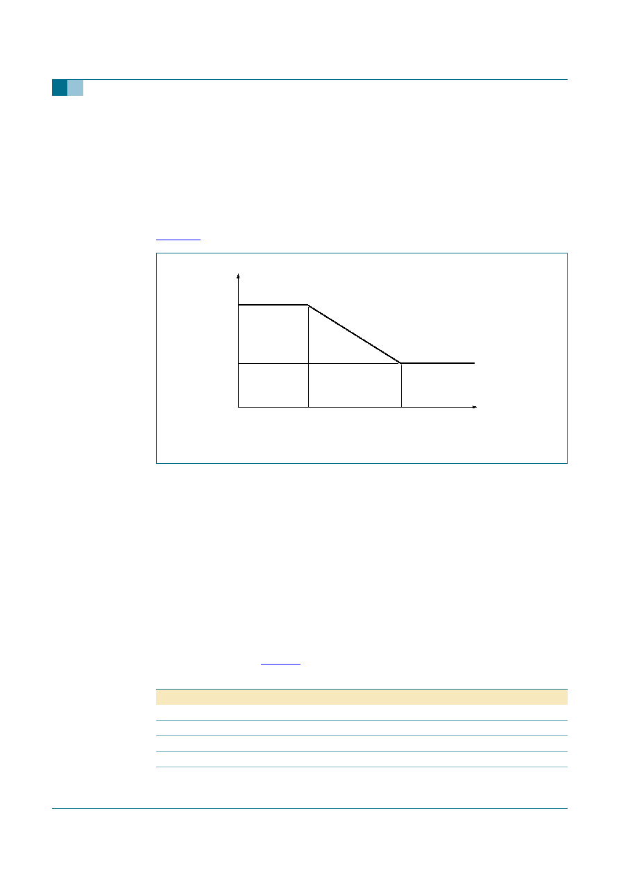
9397 750 13697
� Koninklijke Philips Electronics N.V. 2005. All rights reserved.
Objective data sheet
Rev. 01 -- 20 June 2005
40 of 73
Philips Semiconductors
SAA7806
One chip automotive CD audio device
Another condition that will set both left and right kill signals is the soft mute block reaching
`fully muted' (volume-stage 0).
6.6.7.6
De-emphasis filter
This feature only affects the I
2
S-bus, not the EBU output. The de-emphasis filter can be
used to remove pre-emphasis from tracks which have been recorded making use of the
standard emphasis as described in the CD red book. The de-emphasis filter has the
inverse response of the emphasis characteristics as described in the standard; see
Figure 23
.
Control over the de-emphasis filter is done via FilterConfig(DEEMPHCONTROL). The
filter can be enabled or disabled under software control, or be fully automatic in hardware.
In the latter case, the filter will be turned on when a pre-emphasis bit is detected in the
control byte of the Q-channel subcode, and turned off when this bit is missing.
There are two possible detection modes:
�
According to red book; only a pre-emphasis bit is checked (so is allowed to change)
during the lead-in area, and during pauses between tracks
�
According to orange book; pre-emphasis is checked on every subcode frame.
6.6.7.7
Upsample filter (four times)
This feature only affects the I
2
S-bus, not the EBU output. When it is enabled, the audio
data will be upsampled by a factor of four. The upsampling provides the frequency
response described in
Table 11
.
Fig 23. De-emphasis characteristics
001aab767
= 50
�
s
(3.18 kHz)
= 15
�
s
(10.6 kHz)
frequency
(kHz)
-
10 dB
0 dB
gain
(dB)
Table 11:
Upsample filter frequency response
Pass band
Stop band
Attenuation
0 kHz to 9 kHz
-
0.001 dB
9 kHz to 20 kHz
-
0.03 dB
-
24 kHz
25 dB
-
24 kHz to 27 kHz
38 dB
-
27 kHz to 35 kHz
40 dB

9397 750 13697
� Koninklijke Philips Electronics N.V. 2005. All rights reserved.
Objective data sheet
Rev. 01 -- 20 June 2005
41 of 73
Philips Semiconductors
SAA7806
One chip automotive CD audio device
When upsampling is enabled, the audio data output rate on the I
2
S-bus interface will be
four times higher than without upsampling. Therefore the I
2
S-bus word clock (pin WCLK)
frequency has to be four times higher. This means that the I
2
S-bus bit clock (bclk) speed
needs to be programmed to be four times higher speed then normally required for that
bit-rate when upsampling would be disabled.
Another result of the upsampling is that every sample will have 18 bits precision instead of
16 after the upsample filter. To make use of this extra bit-precision, the user should select
24-bit or 32-bit I
2
S-bus format. When using 16-bit I
2
S-bus format, the 2 lowest bits will not
be output.
6.6.7.8
Data output interfaces
There are 3 interfaces via which data can be output from the channel decoder block.
�
Main data can be output via I
2
S-bus
�
Subcode can be output via the subcode interface
�
Main data + subcode can be output via EBU/SPDIF.
All interfaces can be used at the same time if needed, although there are a few restrictions
on the EBU, see
Section 6.6.7.10 "EBU interface" on page 42
.
6.6.7.9
I
2
S-bus interface
The I
2
S-bus is a 6 wire interface (four main and two subcode). It supports 16-bit, 24-bit
and 32-bit I
2
S-bus and EIAJ (Sony) modes. Timing is shown in
Figure 24
. The required
format can be selected in register IISFormat.
Compliant with the I
2
S-bus specification, the I
2
S-bus signals WCLK, DATA, EF and SYNC
are all clocked on the falling edge of the I
2
S-bus bit clock signal bclk.
-
35 kHz to 64 kHz
50 dB
-
64 kHz to 68 kHz
31 dB
-
68 kHz
35 dB
-
69 kHz to 88 kHz
40 dB
Table 11:
Upsample filter frequency response
...continued
Pass band
Stop band
Attenuation
Fig 24. I
2
S-bus format 1; 16 clocks per word
001aab768
D0
D15
D14
D13
flag - MSB (1 is unreliable)
left
right
flag - LSB
flag - MSB
D12
D11
D10
D9
D8
D7
D6
D5
D4
D3
D2
D1
D0
D15
D14
DATA
bclk
EF
WCLK
SYNC

9397 750 13697
� Koninklijke Philips Electronics N.V. 2005. All rights reserved.
Objective data sheet
Rev. 01 -- 20 June 2005
42 of 73
Philips Semiconductors
SAA7806
One chip automotive CD audio device
�
Bclk: all other I
2
S-bus signals are clocked on bclk
�
WCLK: indicates the start of a new 16/18-bit word on the dataline, and differentiates
between left and right sample
�
DATA: 16/18-bit data words are outputted via this line, 1-bit / bclk-period
�
Error Flag (EF): contains the byte reliability flag; bytes that are indicated as erasures
(possible errors) after C1 and C2 correction, are flagged.
�
SYNC: indicates that the serial subcode line contains the MSB of a subcode word; it
will be asserted every six WCLK periods for half a WCLK period. If a subcode sync is
transferred on the subcode line, this signal will be asserted for a full WCLK period.
The I
2
S-bus interface can either work in master or slave mode. In master mode, the bclk
can be gated off by the channel decoder. In slave mode, the bclk is continuously running.
To prevent the internal FIFO from overflow, the filling of the buffer must be regulated (see
Section "Data latency and FIFO operation" on page 35
).
Bclk and WCLK can either be input (generated outside the channel decoder) or output
(generated internally in the clock control block). Selection can be done via bits WCLKSEL
and BCLKSEL in register IISConfig.
The I
2
S-bus output rate is determined by the speed of the bclk, which is configured via
register BitClockConfig. The I
2
S-bus interface can be configured to run at 1
�
, 2
�
, 4
�
or
6
�
CD (not available for I
2
S-bus 24).
In case of gated bit clock, when BitClockConfig(BCLKGEN) is `1', the speed must be
configured such that the maximum rate available on the bus is 20 % higher than the
average data throughput rate. Or in other words: the bus should have at least 20 % idle
time in between 2 bursts of data.
Default after reset, the I
2
S-bus pins on the IC will be put into 3-state. They can be
activated via register IISConfig. This register also contains the possibility to kill the I
2
S-bus
interface, such that all dataline outputs go LOW.
6.6.7.10
EBU interface
The channel decoder contains a digital one wire EBU or SPDIF output interface. It formats
data according to the IEC60958 specification. The EBU rate can be selected to be 1
�
,
2
�
, 4
�
or 6
�
CD, by programming register EBUClockConfig.
For proper operation of the EBU interface, the I
2
S-bus bit clock must be internally
generated, bitclock gating must be disabled and the following relationship between
EBUClk, bclk, WCLK and I
2
S-bus format must be true:
EBUClk = WCLK
�
64
Some fields in the user channel of the EBU-stream can be filled in by software, configured
via register EBUConfig.
Bit IISConfig(KILLEBU) contains the possibility to `kill' the EBU interface, so that the line
outputs go LOW.

9397 750 13697
� Koninklijke Philips Electronics N.V. 2005. All rights reserved.
Objective data sheet
Rev. 01 -- 20 June 2005
43 of 73
Philips Semiconductors
SAA7806
One chip automotive CD audio device
6.6.7.11
Subcode interface
Subcode data is output via the IISSubo (pin V4) port. This data can be sampled using the
I
2
S-bus SYNC signal (see
Section 6.6.7.9 "I
2
S-bus interface" on page 41
). The SYNC
indicates that the serial subcode line IISSubo contains the MSB of a subcode word. It will
be asserted every six WCLK-periods for half a WCLK-period. If a subcode SYNC is
transferred on the subcode line, this signal will be asserted for a full WCLK period.
During normal operation (upsampling disabled), the subcode output via IISSubo will have
the format as shown in
Figure 25
.
When upsampling is enabled, the I
2
S-bus interface will run at four times the non
upsampled rate. The subcode bit period however will stay at the non-upsampled rate as
shown in
Figure 26
. This means that the IISSubo and SYNC signal will appear to be four
times slower relative to the WCLK. In this case the receiver must use the WCLK divided
by four to sample the subcode.
When slave mode is used, without bclk gating, it is also possible to use the IISSubo output
port as a true single-line interface. In that case the receiver needs to sample the data on
the line with a frequency equal to f
WCLK
�
2 (since subcode is output at a rate of one bit
per half WCLK). Two characteristics of the interface can be used in this case to
synchronize the bit and byte detection in the stream in the absence of a SYNC signal:
�
The first bit (P-bit) of a subcode-byte is used as a start-bit and therefore always `1' (so
no real P-channel information is available on the interface). Between two subcode
bytes there are four zero-bits; this can be used to identify the start of the subcode
bytes within the stream.
Fig 25. Subcode output; upsampling disabled
001aab769
WCLK
IISSubo
SYNC
B6
B5
B4
B3
B2
B1
B0
1 subcode byte every 24 I
2
S-bus bytes
B7
(start)
B6
B5
B4
B7
(start)
Fig 26. Subcode output; upsampling enabled
001aab770
WCLK
IISSubo
SYNC
S0
B7 (start)
B6
B7 (start)
B6
B5
S0
S1
2
�
upsample WCLK
periods (0.5
�
non
upsample WCLK period)
24
�
upsample WCLK periods
(6 x non upsample WCLK periods)
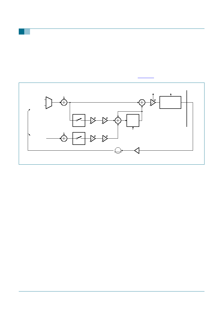
9397 750 13697
� Koninklijke Philips Electronics N.V. 2005. All rights reserved.
Objective data sheet
Rev. 01 -- 20 June 2005
44 of 73
Philips Semiconductors
SAA7806
One chip automotive CD audio device
�
The subcode syncs S0 and S1 are presented as all zeros on the interface (even
P-channel), such that the last subcode byte of a subcode-frame, and the first byte of
the next frame are separated by 28 zero-bits. This can be used to identify the start of
the subcode-frames within the stream.
6.6.8 Motor
A block diagram of the motor interface is given in
Figure 27
.
The motor interface consists of a PI filter and a PDM/PWM modulator. When put in a
closed loop, the motor controller can control both speed, frequency and position error
(FIFOFILL). It can be operated as a P, I or PI controller, by switching on and off the
appropriate switches (
SW1 and SW2).
The frequency and position error integrator gain, K
I
and K
F
, and gain G are
programmable. Frequency and filling set points are also programmable.
The frequency input source can be selected between PLL frequency and 0 Hz. The
position input source is always FIFO filling.
When operated in a stable operation point in closed loop, the motor controller will regulate
the frequency input source and the FIFO filling to their respective set points, this is
implemented by speeding up or slowing down the motor by changing the DC content in
the PDM/PWM output motor signals.
All motor parameters can be configured by programming the motor registers.
6.6.8.1
Frequency set point
When operating the motor in CLV mode, based on EFM, for a certain overspeed, the
motor frequency set point to be programmed is given by
where f
sys
is the system
clock frequency and N the overspeed factor.
Fig 27. Motor servo
001aab771
M
INT
PDM/PWM
MODULATOR
SW1
K
l
K
I
_Mult
SW2
filling
setpoint
0
PLL frequencey
FIFO filling
frequency
setpoint
K
F
K
F
_Mult
overflow
detect
24 T
delay
preset/readback
analog output stage gain
motor
G
G
E
overflow
detect
65,
66
MOTO1,
MOTO2
+
+
-
-
motor frequency set point 7:0
[
]
256
1
N
4.3218
�
10
6
�
2.667
f
sys
�
------------------------------------------
�
�
=

9397 750 13697
� Koninklijke Philips Electronics N.V. 2005. All rights reserved.
Objective data sheet
Rev. 01 -- 20 June 2005
45 of 73
Philips Semiconductors
SAA7806
One chip automotive CD audio device
The set point can be programmed via register MotorFreqSet. The selection of the motor
frequency input is programmed via MotorGainSet2(MotorFreqSource).
6.6.8.2
Position error
The position error will be used to fine tune the motor speed during `slave mode', where the
incoming EFM-bitrate is locked on the programmed fixed I
2
S-bus bclk output speed. The
set point must be chosen between 118 and 128, since this is the usable FIFO size in the
decoder. See
Section "Data latency and FIFO operation" on page 35
for more
information.
The set point can be programmed via register MotorFifoSet.
6.6.8.3
Motor control loop gains (K
P
, K
F
and K
I
)
The control loop gains are all programmable through registers MotorGainSet1 and
MotorGainSet2. To be able to set integrator bandwidth low enough at high system clock
speeds an extra divider for the factors K
I
and K
F
is added. These factors can be written
through the register MotorMultiplier.
The resulting K
I(tot)
is then the K
I
multiplied by K
I
_Mult. The resulting K
F(tot)
is then the K
F
multiplied by K
F
_Mult. The integrator bandwidth must be scaled with the same factor
K
I
_Mult.
Please note the following:
�
K
F
_Mult operates by sampling the input; e.g. for K
F
_Mult = 1, every sample of the
input is passed through the integrator circuit, for a K
F
_Mult of 0.5, every second
sample is passed through, for a K
F
_Mult of 0.25, every fourth sample is passed
through, and so on
�
For a DC input signal, K
F
�
K
F
_Mult should always give the same result. If however,
the input varies quickly, the K
F
�
K
F
_Mult combinations with the same product will not
always give the same result, especially for low values of K
F
_Mult, where the sampling
in the extreme becomes 1 out of every 128 samples. (The input samples to the block
that performs the K
F
_Mult multiplication occur at a rate of 1 sample every 24 system
clock periods.). Sub-sampling might affect the actual resulting gain.
6.6.8.4
Operation modes
The motor controller mode is programmed via register MotorControl. It can operate in
open loop by just sending a fixed power to the motor for start-up and stopping, closed
loop, or shut down. It also selects between PDM and PWM format.
Motor start and stop modes will put a fixed duty cycle PWM or fixed density PDM signal on
the motor outputs. During start or stop, motor speed can be monitored by reading
MotorIntLSB and MotorIntMSB.
MotorOv:
When not setting the appropriate gains in the loop, an overflow might occur
inside the PDM/PWM modulator block, or in the programmable gain stage. This is
signalled by the MotorOv interrupt, which can be read back on InterruptStatus2. The
interrupt disappears when the overflow disappears.
MotorOv can also automatically open
SW1/SW2. This is enabled by writing a `1' to bit
OVFSW in register MotorControl.

9397 750 13697
� Koninklijke Philips Electronics N.V. 2005. All rights reserved.
Objective data sheet
Rev. 01 -- 20 June 2005
46 of 73
Philips Semiconductors
SAA7806
One chip automotive CD audio device
6.6.8.5
Writing and reading motor integrator value
It is possible to obtain the integrator value by reading the registers MotorIntLSB and
MotorIntMSB. The integrator can be written at the same location. By opening all switches,
the user can bypass the whole control and filter part, and just use the block as a DAC for
the motor drivers. The control part can then be done in software.
6.6.8.6
Some notes on application motor servo
The motor servo can be used to control the motor during CLV playback and also during
CAV or pseudo-CLV lock-to-disc or jump mode.
�
In CLV mode, both
SW1 and SW2 must be closed
�
In CAV / pseudo-CLV mode,
SW2 must be open and SW1 may be open
�
The motor servo will revolve the disc at the speed corresponding to the frequency set
point; in CLV mode with lock to EFM, the frequency set point must be set equal to the
desired readout frequency of the HF-PLL
�
Accelerating the disc must be done in one of the start modes
�
Braking the disc must be done in one of the stop modes.
6.7 Digital Servo - PDSIC
The digital servo block on SAA7806 is an evolution of the design used for the SAA7824
IC, and is referred to as Parallel Digital Servo IC (PDSIC). The `parallel' description refers
to the microcontroller interface to the servo block - this is now a high speed parallel
interface, whereas it was previously a serial interface (e.g. a SAA7824 3/4 wire, I
2
C-bus).
The other features of the PDSIC are:
�
Programmable ADC for CD-RW playback compatibility
�
Diode signal processing
�
Signal conditioning
�
Focus and radial control system
�
Access control
�
Sledge control
�
Shock detector
�
Defect detector
�
Off-track counting and detection
�
Automatic closed-loop gain control available for focus and radial loops
�
High-level features.
6.7.1 PDSIC Registers and servo RAM control
The servo block is controlled by two parts of the design - the servo control registers which
are used to control the writing of commands and parameters to the servo; and the servo
RAM. The servo RAM has two roles: storage of the servo parameters and capture of
commands and parameters during the command process.
All of the servo write commands consist of a command byte followed by a number of
parameter bytes (between 1 and 7), all of which have to be loaded into the PDSIC using a
serial communication interface.

9397 750 13697
� Koninklijke Philips Electronics N.V. 2005. All rights reserved.
Objective data sheet
Rev. 01 -- 20 June 2005
47 of 73
Philips Semiconductors
SAA7806
One chip automotive CD audio device
The command byte is the first to be loaded and can be considered as two nibbles. The
upper (most significant) nibble represents the command itself whilst the lower (least
significant) nibble tells the PDSIC how many parameter bytes to expect. The command
byte gets placed into memory location 31h (called oldcom).
Subsequently, parameter bytes get loaded sequentially and these get placed into a stack
space that has been reserved within the memory (locations 30h to 2Bh). With each
parameter byte that is loaded, the value in oldcom is decremented. In other words, the
byte count decreases until it reaches 0, then the PDSIC knows it has a complete servo
command with a command byte and its full complement of parameter bytes. At this point,
the PDSIC acts upon the command and the appropriate function is carried out based
upon the values in the stack space.
There are two special case servo commands: Write_parameter (opcode = A2h) and
Write_decoder_reg (opcode = D1h).
Write_parameter allows the microcontroller to write directly to any memory location. It
carries two parameter bytes; the memory address and the data that is to be written. When
this command is executed the command byte is loaded into oldcom and the first
parameter byte (<RAM_address>) is loaded onto the stack. The second parameter byte
(<data>) is loaded directly into the location specified by <RAM_address>.
Write_decoder_reg allows decoder registers to be written to when the I
2
C-bus interface is
being used. This command carries only one parameter byte, which is the decoder
register/data pair (2 nibbles). When this command is received by the PDSIC, the
register/data pair is loaded into memory location 4Dh.
The servo read commands operate slightly differently in that they carry no parameter
bytes and the lower nibble of the command byte is always 0 to indicate this. When the
PDSIC receives a read command it will make certain information available (mostly from
memory, although some status information is retrieved from the decoder) on the serial
interface for collection by the microcontroller.
If a sequence of values are being read from the servo RAM (e.g. a series of values related
to a PID loop), it is important to ensure that the values are consistent with each other, i.e.
to ensure the servo has not updated some of the values during the period they are read.
Therefore, an interrupt signal is available from the servo to the ARM which raises an IRQ
when it is safe to read related values. This can also be monitored by the state of the servo
register bits SRV_FC0 and SRV_FC1 shown in
Table 13
. The interrupt generator monitors
these signals and raises an IRQ whenever the correct state is achieved. Applying a pulse
to the `inreq_clr' register bit will then clear the interrupt. If the interrupt is not cleared, it will
automatically be reset when the valid reading state is no longer true.
Figure 28
shows the operation of the IRQ signal. Int #1 shows the full duration of an
interrupt that does not get cleared by the ARM. Int #2 and Int #3 are shown being cleared
by pulses being written to the inreq_clr register. The time between interrupts is
approximately 15
�
s and the total interrupt cycle time is approximately 60
�
s.

9397 750 13697
� Koninklijke Philips Electronics N.V. 2005. All rights reserved.
Objective data sheet
Rev. 01 -- 20 June 2005
48 of 73
Philips Semiconductors
SAA7806
One chip automotive CD audio device
6.7.2 Diode signal processing
The photo detector in conventional two-stage three-beam compact disc systems normally
contains six discrete diodes. Four of these diodes (three for single foucault systems) carry
the Central Aperture (CA) signal while the other two diodes (satellite diodes) carry the
radial tracking information. The CA signals are summed into an HF signal for the decoder
function and are also differenced (after analog to digital conversion) to produce the low
frequency focus control signals.
The low frequency content of the six (five if single foucault) photodiode inputs are
converted to PDM bit streams by a multiplexed 6-bit ADC followed by a digital PDM
generation circuit. This supports a range of OPUs in voltage mode mechanisms by having
sixteen selectable gain ranges in two sets, one set for D1 to D4 and the other for R1 and
R2.
6.7.3 Signal conditioning
The digital codes retrieved from the ADC and PDM generator are applied to logic circuitry
to obtain the various control signals. The signals from the central aperture diodes are
processed to obtain a normalized Focus Error (FE) signal:
where the detector set-up is assumed to be as shown in
Figure 29
.
In the case of a single foucault focusing method, the signal conditioning can be switched
under software control such that the signal processing is as follows:
The error signal, FE
n
, is further processed by a Proportional Integral and Differential (PID)
filter section.
Fig 28. Function of servo IRQ signal
001aab772
natural duration of
IRQ (~45
�
s)
int #1
int #2
int #3
IRQ cycle time of ~60
�
s
IRQ cycle time of ~60
�
s
IRQ cycle time of ~60
�
s
IRQ #2
cleared by
inreq_clr
pulse
IRQ #3 cleared by
inreq_clr
pulse
SRV_FC0
SRV_FC1
IRQ
inreq_clr
FE
n
D1
D2
�
D1
D2
+
---------------------
D3
D4
�
D3
D4
+
---------------------
�
=
FE
n
2
D1
D2
�
D1
D2
+
---------------------
�
=

9397 750 13697
� Koninklijke Philips Electronics N.V. 2005. All rights reserved.
Objective data sheet
Rev. 01 -- 20 June 2005
49 of 73
Philips Semiconductors
SAA7806
One chip automotive CD audio device
An internal flag is generated by means of the central aperture signal and an adjustable
reference level. This signal is used to provide extra protection for the Track-Loss (TL)
generation, the focus start-up procedure and the dropout detection.
The radial or tracking error signal is generated by the satellite detector signals R1 and R2.
The Radial Error (RE) signal can be formulated as follows:
where the index `s' indicates the automatic scaling operation which is performed on the
radial error signal. This scaling is necessary to avoid non-optimum dynamic range usage
in the digital representation and reduces the radial bandwidth spread. Furthermore, the
radial error signal will be made free from offset during start-up of the disc.
The four signals from the central aperture detectors, together with the satellite detector
signals generate a Track Position Indicator (TPI) which can be formulated as follows:
where the weighting factor sum_gain is generated internally by the SAA7806 during
initialization.
6.7.4 Focus servo system
6.7.4.1
Focus start-up
Five initially loaded coefficients influence the start-up behavior of the focus controller. The
automatically generated triangular voltage can be influenced by 3 parameters; for height
(ramp_height) and DC offset (ramp_offset) of the triangle and its steepness (ramp_incr).
For protection against false focus point detections, two parameters are available which are
an absolute level on the CA signal (CA_start) and a level on the FE
n
signal (FE_start).
When this CA level is reached then focus has been achieved.
Fig 29. Detector arrangement
RE
s
R1
R2
�
(
)
re_gain
R1
R2
+
(
)
re_offset
�
+
�
=
TPI
sign D1
D2
D3
D4
+
+
+
(
)
R1
R2
+
(
)
sum_gain
�
�
[
]
=
D3
D1
D2
SATELLITE
DIODE R1
SATELLITE
DIODE R2
D1
D3
D2
D4
SATELLITE
DIODE R1
SATELLITE
DIODE R2
D1
D2
D3
D4
SATELLITE
DIODE R1
SATELLITE
DIODE R2
single Foucault
astigmatic focus
double Foucault
mbg422

9397 750 13697
� Koninklijke Philips Electronics N.V. 2005. All rights reserved.
Objective data sheet
Rev. 01 -- 20 June 2005
50 of 73
Philips Semiconductors
SAA7806
One chip automotive CD audio device
When focus is achieved and the level on the FE
n
signal is reached, the focus PID is
enabled to switch on when the next zero crossing is detected in the FE
n
signal.
6.7.4.2
Focus position control loop
The focus control loop contains a digital PID controller which has 5 parameters that are
available to the user. These coefficients influence the integrating (foc_int), proportional
(foc_lead_length, part of foc_parm3) and differentiating (foc_pole_lead, part of
foc_parm1) action of the PID and a digital low-pass filter (foc_pole_noise, part of
foc_parm2) following the PID. The fifth coefficient foc_gain influences the loop gain.
Figure 30
shows the transfer function of the controller, and the coefficients which
determine the behavior.
A simplified block diagram of the focus PID system is given in
Figure 31
.
By using a zero error signal, the actuator position can be held. This action is taken if a
defect or shock is encountered. The PID is followed by a low-pass filter to reduce audible
noise in the control loop.
The desired frequencies for the loop (
1
to
4
) are used to calculate the coefficient values.
Full tables are given in the
Hardware Software Interface (HSI) specification. An
explanation of the parameters in these diagrams is given in
Table 12
.
Fig 30. Bode diagram of focus PID system
Fig 31. Functional diagram of focus PID system
Frequency
(log Hz)
foc_lead_length
foc_pole_lead
foc_pole_noise
001aab773
foc_int
foc_int_strength
I
P
D
Amplitude
(dB)
foc_gain
5
1
2
3
4
001aab774
focus error,
FE
n
P
I
D
zero on
defect
or shock
1/j
j
/
3
1
+
j
/
3
2
/
3
1
4
G
68 FO
focus
actuator
G
E

9397 750 13697
� Koninklijke Philips Electronics N.V. 2005. All rights reserved.
Objective data sheet
Rev. 01 -- 20 June 2005
51 of 73
Philips Semiconductors
SAA7806
One chip automotive CD audio device
[1]
Refer to Table 3 of the
HSI specification.
6.7.4.3
Dropout detection
This detector can be influenced by one parameter (CA_drop). Focus will be lost and the
integrator of the PID will hold if the CA signal drops below this programmable absolute
CA level. When focus is lost it is assumed, initially, to be caused by a black dot.
6.7.4.4
Focus loss detection and fast restart
Whenever focus is lost for longer than approximately 3 ms, it is assumed that the focus
point is lost. A fast restart procedure is initiated which is capable of restarting the focus
loop within 200 ms to 300 ms depending on the programmed coefficients of the
microcontroller.
6.7.4.5
Focus loop gain switching
The gain of the focus control loop (foc_gain) can be multiplied by a factor of 2 or divided
by a factor of 2 during normal operation. The integrator value of the PID is corrected
accordingly. The differentiating (foc_pole_lead) action of the PID can be switched at the
same time as the gain switching is performed.
6.7.4.6
Focus automatic gain control loop
The loop gain of the focus control loop can be corrected automatically to eliminate
tolerances in the focus loop. This gain control injects a signal into the loop which is used to
correct the loop gain. Since this decreases the optimum performance, the gain control
should only be activated for a short time (for example, when starting a new disc).
6.7.5 Radial servo system
6.7.5.1
Radial PID - on-track mode
When the radial servo is in on-track mode (i.e. normal play mode), a PID controller is
active for the fast actuator, while the sledge is steered using either a PI or pulsed-mode
system. A simplified diagram of the radial PID system is given in
Figure 32
:
Table 12:
Focus PID parameters
[1]
Parameter
Controlled by
Comment
1
-
focus integrator bandwidth
2
-
beginning of focus lead
3
foc_parm1
foc_pole_lead; end of focus lead (differentiating part)
4
foc_parm2
foc_pole_noise; low-pass function following PID
3
/
2
foc_parm3
foc_lead_length; lead length (proportional part)
5
= (
1
.
2
/
3
)
foc_int_strength
integrator strength
G
foc_gain
focus loop gain
G
E
end stage gain
defined as peak-to-peak voltage swing over focus
actuator

9397 750 13697
� Koninklijke Philips Electronics N.V. 2005. All rights reserved.
Objective data sheet
Rev. 01 -- 20 June 2005
52 of 73
Philips Semiconductors
SAA7806
One chip automotive CD audio device
An explanation of the different parameters is given below. The frequency response of this
system is given in
Figure 33
:
[1]
Refer to Table 2 of the
HSI specification.
Fig 32. Functional diagram of radial PID system
001aab775
P
D
I
j
/
3
1
+
j
/
3
1/j
NORMALIZER
2
/
3
scaled
radial
error
sledge error signal
zero on
defect
or drop out
1
4
G
67
86
satellite inputs
87
R1
R2
RA
radial
actuator
G
E
Table 13:
Radial PID parameters
[1]
Parameter
Controlled by
Comment
1
-
radial integrator bandwidth
2
-
beginning of radial lead
3
rad_parm_play
end of radial lead (differentiating part)
4
rad_pole_noise
low-pass function following PID
3
/
2
rad_length_lead
lead length (proportional part)
5
= (
1
.
2
/
3
)
rad_int_strength
integrator strength
G
rad_gain
radial loop gain
G
E
end stage gain
defined as peak-to-peak voltage swing over radial
actuator
Fig 33. Bode diagram of radial PID system
frequency
(log Hz)
rad_lead_length
rad_pole_lead
rad_pole_noise
001aab776
rad_int
rad_int_strength
I
5
1
2
3
4
P
D
amplitude
(dB)
rad_gain

9397 750 13697
� Koninklijke Philips Electronics N.V. 2005. All rights reserved.
Objective data sheet
Rev. 01 -- 20 June 2005
53 of 73
Philips Semiconductors
SAA7806
One chip automotive CD audio device
6.7.5.2
Level initialization
During start-up an automatic adjustment procedure is activated to set the values of the
radial error gain (re_gain), offset (re_offset) and satellite sum gain (sum_gain) for TPI
level generation. The initialization procedure runs in a radial open loop situation and is
300 ms. This start-up time period may coincide with the last part of the motor start-up
time period:
�
Automatic gain adjustment: as a result of this initialization the amplitude of the
RE signal is adjusted to within
�
10 % around the nominal RE amplitude
�
Offset adjustment: the additional offset in RE due to the limited accuracy of the
start-up procedure is less than
�
50 nm
�
TPI level generation: the accuracy of the initialization procedure is such that the duty
factor range of TPI becomes 0.4 < duty factor < 0.6 (default duty factor = TPI
HIGH/TPI period).
6.7.5.3
Sledge control
The microcontroller can move the sledge in both directions via the steer sledge command.
6.7.5.4
Tracking control
The actuator is controlled using a PID loop filter with user defined coefficients and gain.
For stable operation between the tracks, the S-curve is extended over 0.75 of the track.
On request from the microcontroller, S-curve extension over 2.25 tracks is used,
automatically changing to access control when exceeding those 2.25 tracks.
Both modes of S-curve extension use a track-count mechanism. In this mode, track
counting results in an `automatic return-to-zero track' to avoid major disturbances in the
audio output and providing improved shock resistance. The sledge is continuously
controlled, or provided with step pulses to reduce power consumption using the filtered
value of the radial PID output. Alternatively, the microcontroller can read the average
voltage on the radial actuator and provide the sledge with step pulses to reduce power
consumption. Filter coefficients of the continuous sledge control can be preset by the
user.
6.7.5.5
Access
The access procedure is divided into two different modes (see
Table 14
), depending on
the requested jump size.
[1]
Microcontroller presettable.
The access procedure makes use of a track counting mechanism, a velocity signal based
on a fixed number of tracks passed within a fixed time interval, a velocity set point
calculated from the number of tracks to go and a user programmable parameter indicating
the maximum sledge performance.
Table 14:
Access types
Access type
Jump size
Access speed
Actuator jump
brake_distance
[1]
decreasing velocity
Sledge jump
brake_distance - 32768
maximum power to sledge

9397 750 13697
� Koninklijke Philips Electronics N.V. 2005. All rights reserved.
Objective data sheet
Rev. 01 -- 20 June 2005
54 of 73
Philips Semiconductors
SAA7806
One chip automotive CD audio device
If the number of tracks remaining is greater than the brake_distance then the sledge jump
mode should be activated or, the actuator jump should be performed. The requested jump
size together with the required sledge breaking distance at maximum access speed
defines the brake_distance value.
During the actuator jump mode, velocity control with a PI controller is used for the
actuator. The sledge is then continuously controlled using the filtered value of the radial
PID output. All filter parameters (for actuator and sledge) are user programmable.
In the sledge jump mode, maximum power (user programmable) is applied to the sledge
in the correct direction while the actuator becomes idle (the contents of the actuator
integrator leaks to zero just after the sledge jump mode is initiated). The actuator can be
electronically damped during sledge jump. The gain of the damping loop is controlled via
the hold_mult parameter.
The fast track jumping circuitry can be enabled or disabled via the xtra_preset parameter.
6.7.5.6
Radial automatic gain control loop
The loop gain of the radial control loop can be corrected automatically to eliminate
tolerances in the radial loop. This gain control injects a signal into the loop which is used
to correct the loop gain. Since this decreases the optimum performance, the gain control
should only be activated for a short time (for example, when starting a new disc).
This gain control differs from the level initialization. The level initialization should be
performed first. The disadvantage of using the level initialization without the gain control is
that only tolerances from the front-end are reduced.
6.7.6 Off-track counting
The Track Position Indicator (TPI) is a flag which is used to indicate whether the radial
spot is positioned on the track, with a margin of
1
/
4
of the track-pitch. In combination with
the Radial Polarity flag (RP) the relative spot position over the tracks can be determined.
These signals can have uncertainties caused by:
�
Disc defects such as scratches and fingerprints
�
The HF information on the disc, which is considered as noise by the detector signals.
In order to determine the spot position with sufficient accuracy, extra conditions are
necessary to generate a Track Loss signal (TL) and an off-track counter value. These
extra conditions influence the maximum speed and this implies that, internally, one of the
following three counting states is selected:
�
Protected state; used in normal play situations; a good protection against false
detection caused by disc defects is important in this state
�
Slow counting state; used in low velocity track jump situations; in this state a fast
response is important rather than the protection against disc defects (if the phase
relationship between TL and RP of
1
/
2
radians is affected too much, then the
direction cannot be determined accurately)
�
Fast counting state; used in high velocity track jump situations; highest obtainable
velocity is the most important feature in this state.
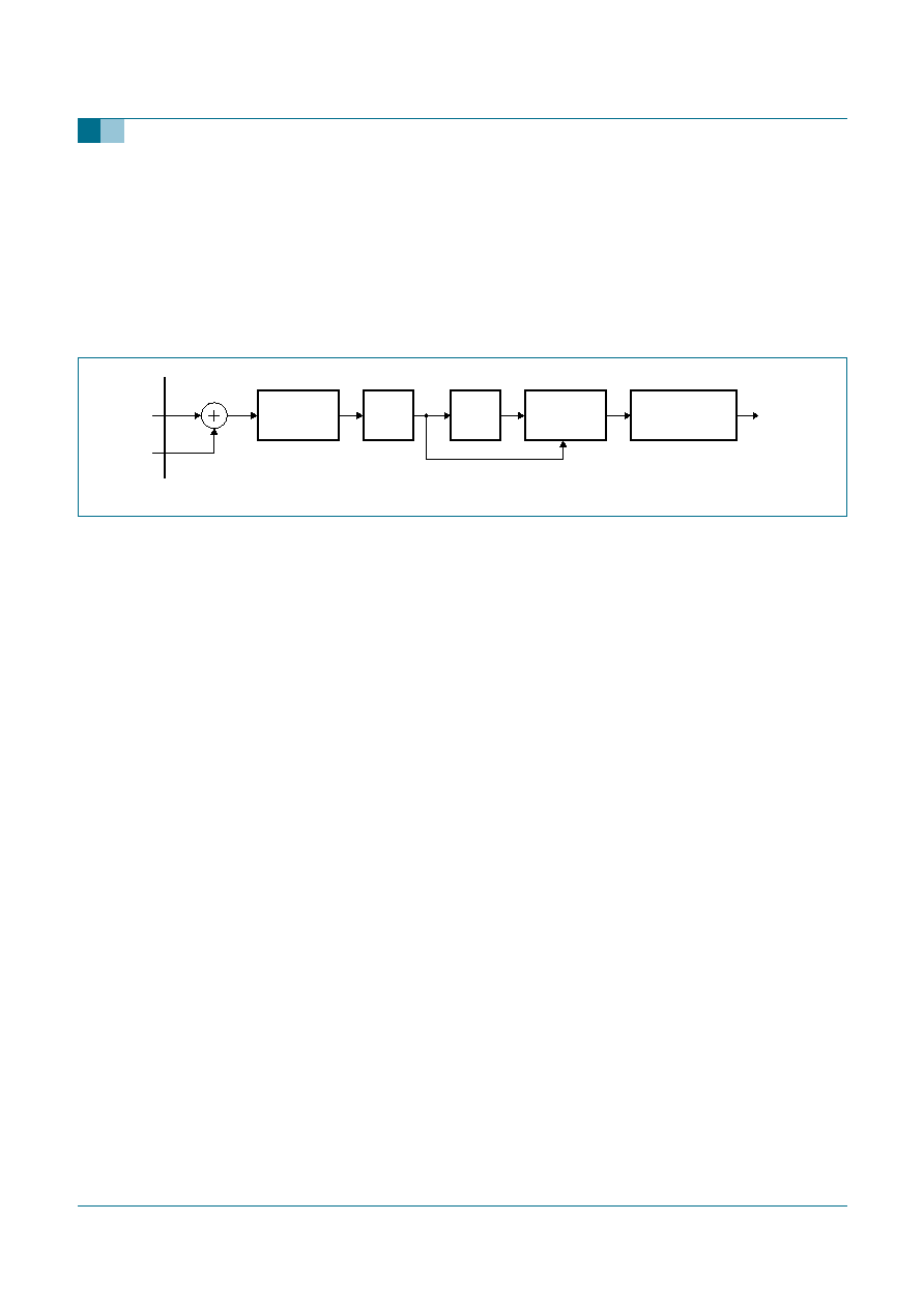
9397 750 13697
� Koninklijke Philips Electronics N.V. 2005. All rights reserved.
Objective data sheet
Rev. 01 -- 20 June 2005
55 of 73
Philips Semiconductors
SAA7806
One chip automotive CD audio device
6.7.7 Defect detection
A defect detection circuit is incorporated into the SAA7806. If a defect is detected, the
radial and focus error signals may be zeroed, resulting in better playability. The defect
detector can be switched off, applied only to focus control or applied to both focus and
radial controls under software control (part of foc_parm1).
The defect detector has programmable set points selectable by the parameter
defect_parm.
6.7.8 Off-track detection
During active radial tracking, off-track detection has been released by continuously
monitoring the off-track counter value. The off-track flag becomes valid whenever the
off-track counter value is not equal to zero. Depending on the type of extended S-curve,
the off-track counter is reset after 0.75 extend or at the original track in the 2.25 track
extend mode.
6.7.9 High level features
6.7.9.1
Automatic error handling
Three watchdogs are present:
�
Focus: detects focus dropout of longer than 3 ms, sets focus lost interrupt, switches
off radial and sledge servos, disables drive to disc motor
�
Radial play: started when radial servo is in on-track mode and a first subcode frame is
found; detects when maximum time between two subcode frames exceeds the time
set by playwatchtime parameter; then sets radial error interrupt, switches radial and
sledge servos off, puts disc motor in jump mode
�
Radial jump: active when radial servo is in long jump or short jump modes; detects
when the off-track counter value decreases by less than 4 tracks between two
readings (time interval set by jumpwatchtime parameter); then sets radial jump error,
switches radial and sledge servos off to cancel jump.
The focus watchdog is always active, the radial watchdogs are selectable via the
radcontrol parameter.
6.7.9.2
Automatic sequencers and timer interrupts
Two automatic sequencers are implemented (and must be initialized after power-on):
�
Autostart sequencer: controls the start-up of focus, radial and motor
�
Autostop sequencer: brakes the disc and shuts down servos.
Fig 34. Defect detector diagram
DECIMATION
FILTER
FAST
FILTER
DEFECT
GENERATION
PROGRAMMABLE
HOLD-OFF
SLOW
FILTER
defect
output
R1
R2
86
87
+
-
001aab777

9397 750 13697
� Koninklijke Philips Electronics N.V. 2005. All rights reserved.
Objective data sheet
Rev. 01 -- 20 June 2005
56 of 73
Philips Semiconductors
SAA7806
One chip automotive CD audio device
When the automatic sequencers are not used it is possible to generate timer interrupts,
defined by the time_parameter coefficient.
6.7.10 Driver interface
The control signals (pins RA, FO and SL) for the mechanism actuators are pulse density
modulated. The modulating frequency can be set to either 1.0584 MHz or 2.1168 MHz;
controlled via the xtra_preset parameter. An analog representation of the output signals
can be achieved by connecting a first-order low-pass filter to the outputs.
During reset (i.e. pin RESET_N is held LOW) the RA, FO, and SL pins are
high-impedance. At all other times, when the laser is switched off, the RA and FO pins
output a 2 MHz, 50 % duty cycle signal.
6.8 Laser interface
The laser diode pre-amp function is built onto the SAA7806 and is illustrated in
Figure 35
.
The current can be regulated, up to 120 mA, in four steps ranging from 58 % up to full
power. The voltage derived from the monitor diode is maintained at a steady state by the
laser drive circuitry, regulating the current through the laser diode.
Fig 35. Laser control circuit
001aab779
UP/DOWN
COUNTER
78
77
76
MONITOR
laser_ion
laser power
Vmon_dac
laser_comp_out
laser_pdmin
laser_clk8MHz
LASER
LPOWER
TIMING AND CONTROL LOGIC
SIGMA
DELTA
DAC
DAC
LASER DIODE
AND
MONITOR
laser_clk32MHz

9397 750 13697
� Koninklijke Philips Electronics N.V. 2005. All rights reserved.
Objective data sheet
Rev. 01 -- 20 June 2005
57 of 73
Philips Semiconductors
SAA7806
One chip automotive CD audio device
6.9 ARM7 system
The following diagram identifies the component parts which make up the system. The
following sections give you a top-level description of the individual blocks.
6.9.1 ARM7TDMI-S microcontroller
The ARM7TDMI-S processor is a member of the ARM family of 32-bit microcontrollers.
The ARM processor offers a high performance for low power consumption and low gate
count. The ARM architecture is based upon Reduced Instruction Set Computer (RISC)
principles. RISC provides the following key benefits:
�
High instruction throughput
�
Excellent real time interrupt response.
[1]
The frequency of operation will depend on the performance required for the SAA7806 application and the
software complexity.
The ARM7TDMI-S processor has 2 instruction sets:
�
The 32-bit ARM instruction set
�
The 16-bit ARM Thumb instruction.
The ARM uses a 3 stage pipeline to increase the throughput of the flow of instructions to
the processor. This allows several operations to operate simultaneously and the processor
and memory systems to operate continuously.
Fig 36. Top level ARM hierarchy
001aab780
ARM7TDMI-S
STATIC
MEMORY
INTERFACE
UNIT
LASER
DRIVER
CHANNEL
DECODER
INTERFACE
32 kB
ROM
INTERFACE
4 kB
RAM
INTERFACE
AHB VPB
BRIDGE
pDSIC
CORE
LCD
DRIVER
AUDIO
DAC
HEADPHONE
VOLUME
CONTROLLER
I
2
S-BUS
I
2
C-BUS
UART
VPB bus
AHB bus
INTERRUPT
CONTROLLER
GPIO
Table 15:
Performance characteristics for ARM7TDMI-S
Process
technology
(
�
m)
Performance
(MIPS/MHz)
Power
consumption
(mW/MHz)
Maximum
operating
frequency
(MHz)
Typical operating frequency
requirements for SAA7806
0.18
0.9
0.39
67
2 MHz
[1]

9397 750 13697
� Koninklijke Philips Electronics N.V. 2005. All rights reserved.
Objective data sheet
Rev. 01 -- 20 June 2005
58 of 73
Philips Semiconductors
SAA7806
One chip automotive CD audio device
The 3 stage pipelines can be defined in the following stages:
�
Fetch cycle; this is used to fetch the instruction from the memory
�
Decode cycle; this is used to decode the registers, used in the instructions fetched
�
Execute cycle; this is used to fetch the data from register banks, the shift and ALU
operations are performed and the data is written back into the memory.
The microcontrollers have traditionally the same width for the instructions and data. The
32-bit architecture can be more efficient in performance and could also address a much
larger address space compared to 16-bit architectures. The code density for 16-bit
architecture would be much higher than 32-bit and the performance would be greater than
half the 32-bit performance.
The ARM Thumb instructions concept addresses the issues when 16-bit instructions are
used but the performance required is for 32-bit architecture. Therefore the aim of Thumb
instruction set can be summarized as follows:
�
Higher performance for 16-bit architecture if 16-bit instructions are to be used.
�
The code density achieved for 16-bit instructions in a 32-bit architecture is a much
more efficient usage of memory space.
6.9.2 Static Memory Interface Unit (SMIU)
The AHB SRAM controller implements an AHB slave interface to an external SRAM. This
interface is only available in the development version of this device. The specification of
this interface is:
�
32-bit AHB interface width
�
67 MHz maximum AHB operating frequency
�
Configured for low latency
�
1 kB memory word depth
�
32-bit data.
6.9.3 ROM Interface
The ROM interface provides an interface between the onboard 4 kB SROM memory and
the ARM via the AHB bus. The specification of this interface is:
�
32-bit AHB interface width
�
67 MHz Maximum AHB operating frequency
�
Configured for low latency
�
8 kB memory word depth
�
32-bit data.
The low latency architecture is optimized for low speed operation. No wait states are used
and the ROM control signals are taken directly from the AHB bus. This means that the
maximum frequency is likely to be limited by the speed at which the control signals arrive
from the AHB master.

9397 750 13697
� Koninklijke Philips Electronics N.V. 2005. All rights reserved.
Objective data sheet
Rev. 01 -- 20 June 2005
59 of 73
Philips Semiconductors
SAA7806
One chip automotive CD audio device
6.9.4 RAM interface
The RAM interface provides an interface between the onboard 32 kB SRAM memory and
the ARM via the AHB bus. The specification of this interface is:
�
32-bit AHB interface width
�
67 MHz maximum AHB operating frequency
�
Configured for low latency
�
1 kB memory word depth
�
32-bit data.
6.9.5 I
2
C-bus interface
This interface can be used as an I
2
C-bus slave or master and is fully compliant with the
I
2
C-bus specification. The specification of this interface is:
�
Master/slave configurations
�
Address 30h
�
67 MHz maximum AHB operating frequency
�
25 MHz I
2
C-bus operating frequency
�
4 byte Rx FIFO depth
�
4 byte Tx FIFO depth
�
Maximum I
2
C-bus frequency of 400 kHz
�
Compatible with 7-bit and 10-bit addressing.
6.9.6 General purpose I/Os
The GPIOs are linked to the VLSI Peripheral Bus (VPB). This interface provides individual
control over each bidirectional pin. Each pin can be configured to be an input, output or
bidirectional:
�
32 bidirectional IOs.
6.9.7 Interrupt controller
�
12 dedicated internal interrupts
�
1 external interrupt which has programmable polarity
�
Two interrupt types available Interrupt Request (IRQ) and Fast Interrupt Request
(FIQ)
�
Interrupts can be defined as IRQ or FIQ
�
One of 16 priority levels can be assigned to an interrupt
�
Interrupt priority threshold level
�
All interrupts can be masked.

9397 750 13697
� Koninklijke Philips Electronics N.V. 2005. All rights reserved.
Objective data sheet
Rev. 01 -- 20 June 2005
60 of 73
Philips Semiconductors
SAA7806
One chip automotive CD audio device
6.9.8 Universal asynchronous receiver transceiver
�
4 byte Tx FIFO depth
�
4 byte Rx FIFO depth
�
Both Rx and Tx can have specific fill levels set before an interrupt is triggered
�
Format of data character to be transmitted or received can be defined.
7.
Limiting values
[1]
All digital input and bidirectional pins are 5 V tolerant
8.
Recommended operating conditions
Table 16:
Limiting values
In accordance with the Absolute Maximum Rating System (IEC 60134).
Symbol Parameter
Conditions
Min
Max
Unit
V
DDD
digital supply voltage
-
0.5
+2.5
V
V
DDP
periphery supply voltage
-
0.5
+3.6
V
V
DDA
analog supply voltage
-
0.5
+3.6
V
V
LCD
analog LCD supply voltage
-
0.5
+5.5
V
V
I
input voltage
analog inputs
-
0.5
V
DDA
+ 0.5 V
5 V tolerant digital inputs
[1]
-
0.5
5.5
V
T
stg
storage temperature
-
55
+125
�
C
P
tot
total power dissipation
playing disc at 1
�
with headphones
enabled
-
274
mW
Table 17:
Characteristics
Symbol
Parameter
Conditions
Min
Typ
Max
Unit
V
DDD
digital supply voltage
1.65
1.80
1.95
V
V
DDP
pad supply voltage
3.0
3.3
3.6
V
V
DDA
analog supply voltage
3.0
3.3
3.6
V
V
LCD
analog LCD supply voltage
4.5
5.0
5.5
V
T
amb
ambient temperature
-
40
-
+85
�
C

9397 750 13697
� Koninklijke Philips Electronics N.V. 2005. All rights reserved.
Objective data sheet
Rev. 01 -- 20 June 2005
61 of 73
Philips Semiconductors
SAA7806
One chip automotive CD audio device
9.
Characteristics
Table 18:
Characteristics
V
DDP
= V
DDA
= 3.0 V to 3.6 V; V
DDD
= 1.65 V to 1.95 V; T
amb
=
-
40
�
C to +85
�
C; unless otherwise specified.
Symbol
Parameter
Conditions
Min
Typ
Max
Unit
Supply
V
DDD
supply voltage, digital regulator
1.65
1.8
1.95
V
V
DDP
supply voltage, digital pads
3.0
3.3
3.6
V
V
DDA
supply voltage, analog
3.0
3.3
3.6
V
I
DDD
supply current, digital
V
DDD
= 1.8 V
[1]
9.6
15.5
42.4
mA
I
DDA
supply current, analog
V
DDA
= 3.3 V
[1] [2]
63.6
63.6
63.6
mA
I
DDP
supply current, peripheral
V
DDP
= 3.3 V
[1] [2]
6.1
6.1
6.1
mA
Voltage regulator
V
DDD
supply voltage, digital core
1.65
1.8
1.95
V
V
DDD(TX)
supply voltage, analog transmitter
1.65
1.8
1.95
V
V
DDD(RX)
supply voltage, analog receiver
1.65
1.8
1.95
V
Analog section (V
DDA
= 3.3 V; V
SSA
= 0 V; T
amb
= 25
�
C)
LF path; input pins R1 and R2
V
i(p)
peak signal amplitude voltage
range (16 steps)
unidirectional
20
-
960
mV
bidirectional
�
20
-
�
960
mV
G
tol
gain tolerance absolute
-
20
-
+20
%
G
tol(ch)
relative gain tolerance between
channels within a pair
-
3
0
+3
%
V
offset(DC)
DC offset cancellation range
relative to full scale
unidirectional
-
�
66
-
%
bidirectional
-
�
33
-
%
G
t
cancellation accuracy
relative to full scale
-
�
4.1
-
%
f
s
sample frequency
-
4.2336
-
MHz
f
i
input frequency (2f
s
)
-
8.4672
-
MHz
B
recovered bandwidth
20
-
-
kHz
S/N
signal-to-noise ratio
0 Hz to 20 kHz
55
-
-
dB
THD
total harmonic distortion
0 Hz to 20 kHz
-
-
-
30
dB
R
i(v)
input resistance in voltage mode
B = 0 Hz to 20 kHz
20
-
-
k
R
i(v)(tol)
voltage mode resistance
tolerance
-
30
-
+30
%
V
cm(min)
minimum input common mode
range
-
1.6
-
V
V
IO
input offset relative to pin
OPU_REF_OUT
-
30
-
+30
mV
HF path; input pins D1, D2, D3 and D4
V
i(ADC)
6-bit ADC input range
peak-to-peak differential
1.4
1.4
1.4
V
V
cm(ADC)
6-bit ADC common mode voltage
2
-
V
B
bandwidth
up to 6
�
(2 MHz x X-rate)
12
-
-
MHz
t
d(
)(f)
phase delay flatness
up to 6
�
(10 ns/X-rate)
-
-
1.66
ns

9397 750 13697
� Koninklijke Philips Electronics N.V. 2005. All rights reserved.
Objective data sheet
Rev. 01 -- 20 June 2005
62 of 73
Philips Semiconductors
SAA7806
One chip automotive CD audio device
S/N
signal-to-noise ratio
100 Hz to 12 MHz
-
-
28
dB
V
o(p-p)
output swing (peak-to-peak
value)
at 6 MHz
-
-
1
V
d
distortion
at 6 MHz
-
-
-
35
dB
PSRR
power supply rejection
40
-
-
dB
G
total gain range
2.4
-
38.4
dB
Z
i
input impedance
nominal
20
20
20
k
B
mon
HF monitor bandwidth
-
3 dB point
27
-
46
MHz
Audio DAC; input/output pin DAC_VREF; output pins DAC_LN, DAC_LP, DAC_RN and DAC_RP
S/N
AW
A-weighted signal-to-noise ratio
-
90
-
dB
THD
total harmonic distortion
at 1 kHz
-
-
-
80
dB
Audio feature; input pins AUX_L and AUX_R
S/N
signal-to-noise ratio
0 Hz to 20 kHz
55
-
-
dB
THD
total harmonic distortion
0 Hz to 20 kHz
-
-
-
30
dB
Headphone buffer; input pins AUX_L and AUX_R; output pins BUF_OUT_L and BUF_OUT_R
G
gain
-
39
-
+6
dB
S/N
AW
A-weighted signal-to-noise ratio
90
-
-
dB
THD
DAC
total harmonic distortion (DAC
input)
at 1 kHz
-
-
-
80
dB
THD
AUX
total harmonic distortion (AUX
input)
at 1 kHz
-
-
-
80
dB
V
O/P(p-p)
O/P voltage swing (peak-to-peak
value)
-
2.2
-
V
Z
i
input impedance
32
-
-
k
Laser driver; input pin MONITOR
l
(o)max
output current
120
-
-
mA
t
su
time for laser to reach final value
1
-
-
ms
V
window
voltage excursion (noise)
-
1
-
+1
mV
V
O
output voltage
sel180 = 0
145
-
155
mV
sel180 = 1
175
-
185
mV
Output pin: OPU_REF_OUT
V
I(ref)
band gap reference voltage
-
1.6
-
V
Oscillator
Input pin OSCIN (external clock)
V
I
input voltage
-
V
DDA
/2
-
V
t
h
input HIGH time
relative to period
45
-
55
%
I
LI
input leakage current
-
20
-
+20
mA
C
I
input capacitance
-
-
7
pF
Table 18:
Characteristics
...continued
V
DDP
= V
DDA
= 3.0 V to 3.6 V; V
DDD
= 1.65 V to 1.95 V; T
amb
=
-
40
�
C to +85
�
C; unless otherwise specified.
Symbol
Parameter
Conditions
Min
Typ
Max
Unit

9397 750 13697
� Koninklijke Philips Electronics N.V. 2005. All rights reserved.
Objective data sheet
Rev. 01 -- 20 June 2005
63 of 73
Philips Semiconductors
SAA7806
One chip automotive CD audio device
Output pin OSCOUT
f
OSCOUT
crystal frequency
[5]
8.4672
-
16.9344 MHz
resonator frequency
8.4672
-
16.9344 MHz
g
m
mutual conductance at start-up
17
-
-
mS
C
F
feedback capacitance
-
-
2
pF
C
O
output capacitance
-
-
7
pF
R
bias
internal bias resistor
-
200
-
k
Pinning characteristics
General
I
OZ
3-state output leakage current
V
O
= 0 V or V
O
= V
DDE
-
-
1
�
A
I
lu
I/O latch-up current
-
0.5
�
V
DDP
< V <
1.5
�
V
DDP
; T
j
< 125
�
C
100
-
-
mA
V
ESD
human body model
-
-
2
kV
machine model
-
-
200
V
Power
I
max
maximum continuous current
-
-
98
mA
Digital pins
DC specifications; input and bidirectional pins
V
IH
HIGH-level input voltage
2.0
-
-
V
V
IL
LOW-level input voltage
-
-
0.8
V
I
IL
LOW-level input current
V
I
= 0 V; no pull up
-
-
1
�
A
I
IH
HIGH-level input current
V
I
= V
DDP
-
-
1
�
A
Parameter for pin types with hysteresis (pin types IDH and IUH)
V
hys
hysteresis voltage
0.4
-
-
V
Parameter for pin types with pull-down (types ID and IDH)
I
pd
pull-down current
V
I
= V
DDP
20
50
75
mA
V
I
= 5 V
20
50
75
mA
Parameter for pin types with pull-up (types BTSU, IU and IUH)
I
pu
pull-up current
V
I
= 0 V
-
13
-
50
-
40
mA
V
DDP
< V
I
< 5.0 V
0
0
0
mA
DC specifications output and bi-directional pins
V
OH
HIGH-level output voltage
V
DDP
-
0.4 -
-
V
V
OL
LOW-level output voltage
-
-
0.4
V
I
OL
LOW-level output current
V
OL
= 0.4 V
5 ns slew rate output
4
-
-
mA
12 mA output
11
-
-
mA
27 mA output
27
-
-
mA
Table 18:
Characteristics
...continued
V
DDP
= V
DDA
= 3.0 V to 3.6 V; V
DDD
= 1.65 V to 1.95 V; T
amb
=
-
40
�
C to +85
�
C; unless otherwise specified.
Symbol
Parameter
Conditions
Min
Typ
Max
Unit

9397 750 13697
� Koninklijke Philips Electronics N.V. 2005. All rights reserved.
Objective data sheet
Rev. 01 -- 20 June 2005
64 of 73
Philips Semiconductors
SAA7806
One chip automotive CD audio device
[1]
V
DDD1
and V
DDD2
.
[2]
Minimum value is initial reset value; primary clock = 67 MHz; AHB and decoder = 4 MHz.
Typical and maximum value with playing CD at 1
�
; headphone buffer enabled; primary clock = 67 MHz.
For typical value, AHB = 16 MHz and decoder = 4 MHz; for maximum value, AHB = 67 MHz and decoder = 4 MHz.
[3]
V
DDA1
, V
DDA2
, V
DDA3
and V
DD(DAC)
.
[4]
V
DDP1
, V
DDP2
and V
DDP3
.
[5]
It is recommended that the nominal running series resistance of the crystal or ceramic resonator is
60
.
I
OH
HIGH-level output current
V
OH
= V
DDP
-
0.4 V
5 ns slew rate output
-
5
-
-
mA
12 mA output
-
13
-
-
mA
27 mA output
-
28
-
-
mA
I
OH(sc)
HIGH-level short-circuit current
short period of time;
V
OH
= 0 V
-
-
-
45
mA
I
OL(sc)
LOW-level short-circuit current
short period of time;
V
OL
= V
DDP
-
-
50
mA
AC specifications; input pins
t
r
, t
f
rise and fall time
-
6
200
ns
AC specifications; output and bidirectional pins
Parameter for pin types with slew rate limited output (types BTS, BTSU and OTS)
t
THL
, t
TLH
transition times
C
L
= 30 pF; transition times
read at 10 % and 90 % of
output slope; 5 ns slew rate
-
4.0
-
ns
Parameter for pin types with slew rate limited output and 12 mA source or sink current (type AOBS)
t
THL
, t
TLH
transition times
C
L
= 30 pF; transition times
read at 10 % and 90 % of
output slope; 5 ns slew rate;
12 mA output
-
2.9
-
ns
Parameter for pin types with 27 mA source or sink current (type OS)
t
THL
, t
TLH
transition times
C
L
= 30 pF; transition times
read at 10 % and 90 % of
output slope; 27 mA output
-
3.8
-
ns
Table 18:
Characteristics
...continued
V
DDP
= V
DDA
= 3.0 V to 3.6 V; V
DDD
= 1.65 V to 1.95 V; T
amb
=
-
40
�
C to +85
�
C; unless otherwise specified.
Symbol
Parameter
Conditions
Min
Typ
Max
Unit

xxxx xxxxxxxxxxxxxxxxxxxxxxxxxxxxxx x xxxxxxxxxxxxxx xxxxxxxxxx xxx xxxxxx xxxxxxxxxxxxxxxxxxxxxxx xxxxxxxxxxxxxxxxxxxxxx
xxxxx xxxxxx xx xxxxxxxxxxxxxxxxxxxxxxxxxxxxx xxxxxxxxxxxxxxxxxxxxxx xxxxxxxxxxx xxxxxxx xxxxxxxxxxxxxxxxxxx
xxxxxxxxxxxxxxxx xxxxxxxxxxxxxx xxxxxx xx xxxxxxxxxxxxxxxxxxxxxxxxxxxxxxxx xxxxxxxxxxxxxxxxxxxxxxxx xxxxxxx
xxxxxxxxxxxxxxxxxxxxxxxxxxxxxxxxxxxxxxxxxxxxxx xxxxxxxxxxx xxxxx x x
9397 750 13697
� K
oninklijk
e Philips Electronics N.V
. 2005. All r
ights reser
v
ed.
Objective data sheet
Re
v
.
01 -- 20 J
une 2005
65 of 73
Philips Semiconductor
s
SAA7806
One c
hip automotive CD audio de
vice
10.
Application inf
ormation
Fig 37. Typical application diagram
SAA7806
81
1
2
3
4
5
6
7
8
9
10 11 12 13 14 15 16 17 18 19 20 21 22 23 24 25 26 27 28 29 30
80 79 78 77 76 75 74 73 72 71 70 69 68 67 66 65 64 63 62 61 60 59 58 57 56 55 54 53 52 51
82
83
84
85
86
87
88
89
90
91
92
93
94
95
96
97
98
99
100
V
DDA1
D1
D2
D3
D4
R1
R2
AUX_L
AUX_R
V
DDA2
OPU_REF_OUT
V
SSA2
OSCOUT
OSCIN
V
DD(DAC)
DAC_LP
DAC_LN
DAC_VREF
DAC_RN
DAC_RP
V
SS(D
A
CF)
V
SS(D
A
CB)
BUF_OUT_L
BUF_OUT_R
V
DD
A3
A_IN_1/GPIO0
A_IN_2/GPIO1
TX/GPIO_ANA
RX/GPIO_ANA
SDA
SCL
V
SSD1
RESET_N
V
DD1
LKILL
RKILL
V
SSP1
DOBM
V
DDP1
SEG0/GPIO4
SEG1/GPIO5
SEG2/GPIO6
SEG3/GPIO7
SEG4/GPIO8
SEG5/GPIO9
SEG6/GPIO10
SEG7/GPIO11
SEG8/GPIO12
SEG9/GPIO13
V
LCD
HF_MON
V
SSA1
MONITOR
LASER
LPOWER
TDO2/GPIO31
INT/GPIO30/RTCK
TMS2/GPIO29
TDI2/GPIO28
V
DDD2
V
SSD2
SL
FO
RA
MOTO2
MOTO1
TD0
TRST_N
TCK
TMS
TDI
V
DDP3
V
SSP3
V4/CL16
SYNC
SCLK
WCLK
DATA
EF
SDI
50
49
48
47
46
45
44
43
42
41
40
39
38
37
36
35
34
33
32
31
SCLI
3.3 V
1.8 V
R5
R4
R3
R2
R11
10 k
R12
10 k
mute
C2
C1
C12
4.7 nF
C5
33 pF
C6
33 pF
8.4672 MHz
left
right
DAC out
G1
C10
4.7 nF
C8
10 nF
C9
10 nF
C7
1
�
F
R10
2.7 k
C11
4.7 nF
C3
C4
JTAG port
sledge
OPU connections
focus
radial
spindle
3.3 V
WCLI
V
DDP2
INT_EX_ROM
V
SSP2
COM3/GPIO27
COM2/GPIO26
COM1/GPIO25
COM0/GPIO24
SEG19/GPIO23/GFLG
SEG18/GPIO22/MEAS
SEG17/GPIO21/CL1
001aac132
SEG16/GPIO20
SEG15/GPIO19
V
DD(LED)
SEG14/GPIO18
3.3 V
SEG13/GPIO17
SEG12/GPIO16
SEG11/GPIO15
SEG10/GPIO14
reset
1.8 V
R1
10 k
optional
DRIVER
U2
M
1
2
3
4
5
6
7
8
9
10
11
12
13
14
28
27
26
25
24
23
22
29
30
21
20
19
18
17
16
15
V
CC
RADOUTN
FOCOUTP
GND
FOCOUTN
RADOUTP
V
CC
V
CC
SLOUTP
SLOUTN
GND
MOTOUTP
MOTOUTN
V
CC
VOUT3.3
VFBIN3.3
VOUT1.8
VFBIN1.8
MUTE
RADIN
FOCIN
GND
SLIN
VBIASIN
GND
VBIASOUT
MOTBIAS
MOTIN1
MOTIN2
spindle
R8
R9
R6
R7
sledge
focus
radial
3.3 V
V1 BC337
V2 BC337
1.8 V
3.3 V
8 V
TR2
focus
radial
OPU
servos
SP2
TR1
TR MO
SP MO
SP1
GND
M
3.3 V
pin 81
C13
22
�
F
(25 V)
C14
2.2 nF
3.3 V
pin 90
C15
22
�
F
(25 V)
C16
2.2 nF
3.3 V
pin 95
C17
22
�
F
(25 V)
C18
2.2 nF
3.3 V
supply decoupling
pin 5
C19
22
�
F
(25 V)
C20
2.2 nF
3.3 V
pin 19
C21
22
�
F
(25 V)
C22
2.2 nF
3.3 V
pin 48
C23
22
�
F
(25 V)
C24
2.2 nF
3.3 V
pin 59
C25
22
�
F
(25 V)
C26
2.2 nF
3.3 V
pin 76
C27
22
�
F
(25 V)
C28
2.2 nF
1.8 V
pin 14
C31
22
�
F
(25 V)
C32
2.2 nF
1.8 V
pin 71
C33
22
�
F
(25 V)
C34
2.2 nF
3.3 V
pin 76
C35
22
�
F
(25 V)
C36
2.2 nF
3.3 V
pin 36
C29
100 nF

9397 750 13697
� Koninklijke Philips Electronics N.V. 2005. All rights reserved.
Objective data sheet
Rev. 01 -- 20 June 2005
66 of 73
Philips Semiconductors
SAA7806
One chip automotive CD audio device
11. Package outline
Fig 38. Package outline SOT317-2 (QFP100)
UNIT
A
1
A
2
A
3
b
p
c
E
(1)
e
H
E
L
L
p
Z
y
w
v
REFERENCES
OUTLINE
VERSION
EUROPEAN
PROJECTION
ISSUE DATE
IEC
JEDEC
JEITA
mm
0.25
0.05
2.90
2.65
0.25
0.40
0.25
0.25
0.14
14.1
13.9
0.65
18.2
17.6
1.0
0.6
7
0
o
o
0.15
0.1
0.2
1.95
DIMENSIONS (mm are the original dimensions)
Note
1. Plastic or metal protrusions of 0.25 mm maximum per side are not included.
1.0
0.6
SOT317-2
MO-112
99-12-27
03-02-25
D
(1)
(1)
(1)
20.1
19.9
H
D
24.2
23.6
E
Z
0.8
0.4
D
e
E
A
1
A
L
p
detail X
L
(A )
3
B
30
c
b
p
E
H
A
2
D
Z D
A
Z E
e
v
M
A
1
100
81
80
51
50
31
pin 1 index
X
y
b
p
D
H
v
M
B
w
M
w
M
0
5
10 mm
scale
QFP100: plastic quad flat package; 100 leads (lead length 1.95 mm); body 14 x 20 x 2.8 mm
SOT317-2
A
max.
3.2

9397 750 13697
� Koninklijke Philips Electronics N.V. 2005. All rights reserved.
Objective data sheet
Rev. 01 -- 20 June 2005
67 of 73
Philips Semiconductors
SAA7806
One chip automotive CD audio device
12. Soldering
12.1 Introduction to soldering surface mount packages
This text gives a very brief insight to a complex technology. A more in-depth account of
soldering ICs can be found in our
Data Handbook IC26; Integrated Circuit Packages
(document order number 9398 652 90011).
There is no soldering method that is ideal for all surface mount IC packages. Wave
soldering can still be used for certain surface mount ICs, but it is not suitable for fine pitch
SMDs. In these situations reflow soldering is recommended.
12.2 Reflow soldering
Reflow soldering requires solder paste (a suspension of fine solder particles, flux and
binding agent) to be applied to the printed-circuit board by screen printing, stencilling or
pressure-syringe dispensing before package placement. Driven by legislation and
environmental forces the worldwide use of lead-free solder pastes is increasing.
Several methods exist for reflowing; for example, convection or convection/infrared
heating in a conveyor type oven. Throughput times (preheating, soldering and cooling)
vary between 100 seconds and 200 seconds depending on heating method.
Typical reflow peak temperatures range from 215
�
C to 270
�
C depending on solder paste
material. The top-surface temperature of the packages should preferably be kept:
�
below 225
�
C (SnPb process) or below 245
�
C (Pb-free process)
� for all BGA, HTSSON..T and SSOP..T packages
� for packages with a thickness
2.5 mm
� for packages with a thickness < 2.5 mm and a volume
350 mm
3
so called
thick/large packages.
�
below 240
�
C (SnPb process) or below 260
�
C (Pb-free process) for packages with a
thickness < 2.5 mm and a volume < 350 mm
3
so called small/thin packages.
Moisture sensitivity precautions, as indicated on packing, must be respected at all times.
12.3 Wave soldering
Conventional single wave soldering is not recommended for surface mount devices
(SMDs) or printed-circuit boards with a high component density, as solder bridging and
non-wetting can present major problems.
To overcome these problems the double-wave soldering method was specifically
developed.
If wave soldering is used the following conditions must be observed for optimal results:
�
Use a double-wave soldering method comprising a turbulent wave with high upward
pressure followed by a smooth laminar wave.
�
For packages with leads on two sides and a pitch (e):
� larger than or equal to 1.27 mm, the footprint longitudinal axis is preferred to be
parallel to the transport direction of the printed-circuit board;

9397 750 13697
� Koninklijke Philips Electronics N.V. 2005. All rights reserved.
Objective data sheet
Rev. 01 -- 20 June 2005
68 of 73
Philips Semiconductors
SAA7806
One chip automotive CD audio device
� smaller than 1.27 mm, the footprint longitudinal axis must be parallel to the
transport direction of the printed-circuit board.
The footprint must incorporate solder thieves at the downstream end.
�
For packages with leads on four sides, the footprint must be placed at a 45
�
angle to
the transport direction of the printed-circuit board. The footprint must incorporate
solder thieves downstream and at the side corners.
During placement and before soldering, the package must be fixed with a droplet of
adhesive. The adhesive can be applied by screen printing, pin transfer or syringe
dispensing. The package can be soldered after the adhesive is cured.
Typical dwell time of the leads in the wave ranges from 3 seconds to 4 seconds at 250
�
C
or 265
�
C, depending on solder material applied, SnPb or Pb-free respectively.
A mildly-activated flux will eliminate the need for removal of corrosive residues in most
applications.
12.4 Manual soldering
Fix the component by first soldering two diagonally-opposite end leads. Use a low voltage
(24 V or less) soldering iron applied to the flat part of the lead. Contact time must be
limited to 10 seconds at up to 300
�
C.
When using a dedicated tool, all other leads can be soldered in one operation within
2 seconds to 5 seconds between 270
�
C and 320
�
C.
12.5 Package related soldering information
[1]
For more detailed information on the BGA packages refer to the
(LF)BGA Application Note (AN01026);
order a copy from your Philips Semiconductors sales office.
[2]
All surface mount (SMD) packages are moisture sensitive. Depending upon the moisture content, the
maximum temperature (with respect to time) and body size of the package, there is a risk that internal or
external package cracks may occur due to vaporization of the moisture in them (the so called popcorn
effect). For details, refer to the Drypack information in the
Data Handbook IC26; Integrated Circuit
Packages; Section: Packing Methods.
[3]
These transparent plastic packages are extremely sensitive to reflow soldering conditions and must on no
account be processed through more than one soldering cycle or subjected to infrared reflow soldering with
peak temperature exceeding 217
�
C
�
10
�
C measured in the atmosphere of the reflow oven. The package
body peak temperature must be kept as low as possible.
Table 19:
Suitability of surface mount IC packages for wave and reflow soldering methods
Package
[1]
Soldering method
Wave
Reflow
[2]
BGA, HTSSON..T
[3]
, LBGA, LFBGA, SQFP,
SSOP..T
[3]
, TFBGA, VFBGA, XSON
not suitable
suitable
DHVQFN, HBCC, HBGA, HLQFP, HSO, HSOP,
HSQFP, HSSON, HTQFP, HTSSOP, HVQFN,
HVSON, SMS
not suitable
[4]
suitable
PLCC
[5]
, SO, SOJ
suitable
suitable
LQFP, QFP, TQFP
not recommended
[5] [6]
suitable
SSOP, TSSOP, VSO, VSSOP
not recommended
[7]
suitable
CWQCCN..L
[8]
, PMFP
[9]
, WQCCN..L
[8]
not suitable
not suitable

9397 750 13697
� Koninklijke Philips Electronics N.V. 2005. All rights reserved.
Objective data sheet
Rev. 01 -- 20 June 2005
69 of 73
Philips Semiconductors
SAA7806
One chip automotive CD audio device
[4]
These packages are not suitable for wave soldering. On versions with the heatsink on the bottom side, the
solder cannot penetrate between the printed-circuit board and the heatsink. On versions with the heatsink
on the top side, the solder might be deposited on the heatsink surface.
[5]
If wave soldering is considered, then the package must be placed at a 45
�
angle to the solder wave
direction. The package footprint must incorporate solder thieves downstream and at the side corners.
[6]
Wave soldering is suitable for LQFP, QFP and TQFP packages with a pitch (e) larger than 0.8 mm; it is
definitely not suitable for packages with a pitch (e) equal to or smaller than 0.65 mm.
[7]
Wave soldering is suitable for SSOP, TSSOP, VSO and VSSOP packages with a pitch (e) equal to or larger
than 0.65 mm; it is definitely not suitable for packages with a pitch (e) equal to or smaller than 0.5 mm.
[8]
Image sensor packages in principle should not be soldered. They are mounted in sockets or delivered
pre-mounted on flex foil. However, the image sensor package can be mounted by the client on a flex foil by
using a hot bar soldering process. The appropriate soldering profile can be provided on request.
[9]
Hot bar soldering or manual soldering is suitable for PMFP packages.
13. Glossary
AHB -- ARM Advanced High Performance Bus
ARM -- Advanced RISC Machines (32-bit microcontroller design)
ARM7TDMI-S -- Specific version of ARM microcontroller used in SAA7806 (ARM7
family)
FIFO -- First in, first out
GPIO -- General purpose input/output
HSI -- Hardware Software Interface specification
I
2
C -- Inter IC-bus Communication format
I
2
S -- Inter IC Sound format
LCD -- Liquid Crystal Display
PDSIC -- Parallel Digital Servo IC (digital servo block within SAA7806)
RISC -- Reduced Instruction Set Computer
Thumb -- ARM 16-bit instruction set
UART -- Universal Asynchronous Receiver Transmitter
VPB -- VLSI Peripheral Bus

9397 750 13697
� Koninklijke Philips Electronics N.V. 2005. All rights reserved.
Objective data sheet
Rev. 01 -- 20 June 2005
70 of 73
Philips Semiconductors
SAA7806
One chip automotive CD audio device
14. Revision history
Table 20:
Revision history
Document ID
Release date
Data sheet status
Change notice
Doc. number
Supersedes
SAA7806_1
20050620
Objective data sheet
-
9397 750 13697
-

Philips Semiconductors
SAA7806
One chip automotive CD audio device
9397 750 13697
� Koninklijke Philips Electronics N.V. 2005. All rights reserved.
Objective data sheet
Rev. 01 -- 20 June 2005
71 of 73
15. Data sheet status
[1]
Please consult the most recently issued data sheet before initiating or completing a design.
[2]
The product status of the device(s) described in this data sheet may have changed since this data sheet was published. The latest information is available on the Internet at
URL http://www.semiconductors.philips.com.
[3]
For data sheets describing multiple type numbers, the highest-level product status determines the data sheet status.
16. Definitions
Short-form specification -- The data in a short-form specification is
extracted from a full data sheet with the same type number and title. For
detailed information see the relevant data sheet or data handbook.
Limiting values definition -- Limiting values given are in accordance with
the Absolute Maximum Rating System (IEC 60134). Stress above one or
more of the limiting values may cause permanent damage to the device.
These are stress ratings only and operation of the device at these or at any
other conditions above those given in the Characteristics sections of the
specification is not implied. Exposure to limiting values for extended periods
may affect device reliability.
Application information -- Applications that are described herein for any
of these products are for illustrative purposes only. Philips Semiconductors
make no representation or warranty that such applications will be suitable for
the specified use without further testing or modification.
17. Disclaimers
Life support -- These products are not designed for use in life support
appliances, devices, or systems where malfunction of these products can
reasonably be expected to result in personal injury. Philips Semiconductors
customers using or selling these products for use in such applications do so
at their own risk and agree to fully indemnify Philips Semiconductors for any
damages resulting from such application.
Right to make changes -- Philips Semiconductors reserves the right to
make changes in the products - including circuits, standard cells, and/or
software - described or contained herein in order to improve design and/or
performance. When the product is in full production (status `Production'),
relevant changes will be communicated via a Customer Product/Process
Change Notification (CPCN). Philips Semiconductors assumes no
responsibility or liability for the use of any of these products, conveys no
license or title under any patent, copyright, or mask work right to these
products, and makes no representations or warranties that these products are
free from patent, copyright, or mask work right infringement, unless otherwise
specified.
18. Trademarks
Notice -- All referenced brands, product names, service names and
trademarks are the property of their respective owners.
I
2
C-bus -- wordmark and logo are trademarks of Koninklijke Philips
Electronics N.V.
19. Contact information
For additional information, please visit: http://www.semiconductors.philips.com
For sales office addresses, send an email to: sales.addresses@www.semiconductors.philips.com
Level
Data sheet status
[1]
Product status
[2] [3]
Definition
I
Objective data
Development
This data sheet contains data from the objective specification for product development. Philips
Semiconductors reserves the right to change the specification in any manner without notice.
II
Preliminary data
Qualification
This data sheet contains data from the preliminary specification. Supplementary data will be published
at a later date. Philips Semiconductors reserves the right to change the specification without notice, in
order to improve the design and supply the best possible product.
III
Product data
Production
This data sheet contains data from the product specification. Philips Semiconductors reserves the
right to make changes at any time in order to improve the design, manufacturing and supply. Relevant
changes will be communicated via a Customer Product/Process Change Notification (CPCN).

Philips Semiconductors
SAA7806
One chip automotive CD audio device
9397 750 13697
� Koninklijke Philips Electronics N.V. 2005. All rights reserved.
Objective data sheet
Rev. 01 -- 20 June 2005
72 of 73
continued >>
20. Contents
1
General description . . . . . . . . . . . . . . . . . . . . . . 1
2
Features . . . . . . . . . . . . . . . . . . . . . . . . . . . . . . . 1
2.1
Hardware features . . . . . . . . . . . . . . . . . . . . . . 1
2.2
Read formats . . . . . . . . . . . . . . . . . . . . . . . . . . 2
3
Ordering information . . . . . . . . . . . . . . . . . . . . . 3
4
Block diagram . . . . . . . . . . . . . . . . . . . . . . . . . . 3
5
Pinning information . . . . . . . . . . . . . . . . . . . . . . 4
5.1
Pinning . . . . . . . . . . . . . . . . . . . . . . . . . . . . . . . 4
5.2
Pin description . . . . . . . . . . . . . . . . . . . . . . . . . 5
6
Functional description . . . . . . . . . . . . . . . . . . . 8
6.1
Analog data acquisition. . . . . . . . . . . . . . . . . . . 8
6.1.1
LF acquisition . . . . . . . . . . . . . . . . . . . . . . . . . . 8
6.1.2
HF acquisition . . . . . . . . . . . . . . . . . . . . . . . . . . 9
6.2
Analog clock generation . . . . . . . . . . . . . . . . . 10
6.3
General purpose analog inputs . . . . . . . . . . . 11
6.4
Auxiliary analog inputs . . . . . . . . . . . . . . . . . . 11
6.5
AHB core clock generation . . . . . . . . . . . . . . . 14
6.6
Channel decoder . . . . . . . . . . . . . . . . . . . . . . 14
6.6.1
Features . . . . . . . . . . . . . . . . . . . . . . . . . . . . . 14
6.6.2
Block diagram . . . . . . . . . . . . . . . . . . . . . . . . . 15
6.6.3
Clock control . . . . . . . . . . . . . . . . . . . . . . . . . . 17
6.6.3.1
Signal xclk. . . . . . . . . . . . . . . . . . . . . . . . . . . . 18
6.6.3.2
Sysclock domain. . . . . . . . . . . . . . . . . . . . . . . 18
6.6.3.3
Bitclock domain. . . . . . . . . . . . . . . . . . . . . . . . 18
6.6.3.4
Ebuclock domain . . . . . . . . . . . . . . . . . . . . . . 18
6.6.4
Decoder to ARM microcontroller interface . . . 19
6.6.4.1
Programming interface . . . . . . . . . . . . . . . . . . 19
6.6.4.2
Interrupt strategy. . . . . . . . . . . . . . . . . . . . . . . 19
6.6.5
EFM bit detection and demodulation . . . . . . . 19
6.6.5.1
Signal conditioning . . . . . . . . . . . . . . . . . . . . . 20
6.6.5.2
Bit detector . . . . . . . . . . . . . . . . . . . . . . . . . . . 26
6.6.5.3
Limiting the PLL frequency range . . . . . . . . . . 29
6.6.5.4
Run length 2 pushback detector . . . . . . . . . . . 30
6.6.5.5
Available signals for monitoring . . . . . . . . . . . 30
6.6.5.6
Format of the measurement signal on
MEAS pin . . . . . . . . . . . . . . . . . . . . . . . . . . . . 31
6.6.5.7
Demodulator . . . . . . . . . . . . . . . . . . . . . . . . . . 32
6.6.5.8
EFM demodulation . . . . . . . . . . . . . . . . . . . . . 32
6.6.5.9
Sync detection and synchronization . . . . . . . . 32
6.6.5.10
Sync protection . . . . . . . . . . . . . . . . . . . . . . . . 32
6.6.6
CD decoding . . . . . . . . . . . . . . . . . . . . . . . . . . 33
6.6.6.1
General . . . . . . . . . . . . . . . . . . . . . . . . . . . . . . 33
6.6.6.2
Q-channel subcode interface . . . . . . . . . . . . . 33
6.6.6.3
CD-TEXT interface . . . . . . . . . . . . . . . . . . . . . 34
6.6.6.4
Main data decoding . . . . . . . . . . . . . . . . . . . . 35
6.6.6.5
Error corrector statistics . . . . . . . . . . . . . . . . . 37
6.6.7
Audio back-end and data output interfaces . . 37
6.6.7.1
Audio processing . . . . . . . . . . . . . . . . . . . . . . 38
6.6.7.2
Interpolate and hold . . . . . . . . . . . . . . . . . . . . 38
6.6.7.3
Soft mute and error detection. . . . . . . . . . . . . 39
6.6.7.4
Hard mute on EBU . . . . . . . . . . . . . . . . . . . . . 39
6.6.7.5
Silence detection and kill generation . . . . . . . 39
6.6.7.6
De-emphasis filter . . . . . . . . . . . . . . . . . . . . . 40
6.6.7.7
Upsample filter (four times) . . . . . . . . . . . . . . 40
6.6.7.8
Data output interfaces . . . . . . . . . . . . . . . . . . 41
6.6.7.9
I
2
S-bus interface. . . . . . . . . . . . . . . . . . . . . . . 41
6.6.7.10
EBU interface . . . . . . . . . . . . . . . . . . . . . . . . . 42
6.6.7.11
Subcode interface . . . . . . . . . . . . . . . . . . . . . 43
6.6.8
Motor . . . . . . . . . . . . . . . . . . . . . . . . . . . . . . . 44
6.6.8.1
Frequency set point . . . . . . . . . . . . . . . . . . . . 44
6.6.8.2
Position error . . . . . . . . . . . . . . . . . . . . . . . . . 45
6.6.8.3
Motor control loop gains (K
P
, K
F
and K
I
). . . . . 45
6.6.8.4
Operation modes . . . . . . . . . . . . . . . . . . . . . . 45
6.6.8.5
Writing and reading motor integrator value . . 46
6.6.8.6
Some notes on application motor servo. . . . . 46
6.7
Digital Servo - PDSIC. . . . . . . . . . . . . . . . . . . 46
6.7.1
PDSIC Registers and servo RAM control . . . 46
6.7.2
Diode signal processing . . . . . . . . . . . . . . . . . 48
6.7.3
Signal conditioning . . . . . . . . . . . . . . . . . . . . . 48
6.7.4
Focus servo system . . . . . . . . . . . . . . . . . . . . 49
6.7.4.1
Focus start-up . . . . . . . . . . . . . . . . . . . . . . . . 49
6.7.4.2
Focus position control loop. . . . . . . . . . . . . . . 50
6.7.4.3
Dropout detection. . . . . . . . . . . . . . . . . . . . . . 51
6.7.4.4
Focus loss detection and fast restart . . . . . . . 51
6.7.4.5
Focus loop gain switching . . . . . . . . . . . . . . . 51
6.7.4.6
Focus automatic gain control loop . . . . . . . . . 51
6.7.5
Radial servo system. . . . . . . . . . . . . . . . . . . . 51
6.7.5.1
Radial PID - on-track mode . . . . . . . . . . . . . . 51
6.7.5.2
Level initialization . . . . . . . . . . . . . . . . . . . . . . 53
6.7.5.3
Sledge control . . . . . . . . . . . . . . . . . . . . . . . . 53
6.7.5.4
Tracking control . . . . . . . . . . . . . . . . . . . . . . . 53
6.7.5.5
Access . . . . . . . . . . . . . . . . . . . . . . . . . . . . . . 53
6.7.5.6
Radial automatic gain control loop . . . . . . . . . 54
6.7.6
Off-track counting . . . . . . . . . . . . . . . . . . . . . . 54
6.7.7
Defect detection . . . . . . . . . . . . . . . . . . . . . . . 55
6.7.8
Off-track detection . . . . . . . . . . . . . . . . . . . . . 55
6.7.9
High level features . . . . . . . . . . . . . . . . . . . . . 55
6.7.9.1
Automatic error handling . . . . . . . . . . . . . . . . 55
6.7.9.2
Automatic sequencers and timer interrupts . . 55
6.7.10
Driver interface . . . . . . . . . . . . . . . . . . . . . . . . 56
6.8
Laser interface . . . . . . . . . . . . . . . . . . . . . . . . 56
6.9
ARM7 system. . . . . . . . . . . . . . . . . . . . . . . . . 57
6.9.1
ARM7TDMI-S microcontroller . . . . . . . . . . . . 57
6.9.2
Static Memory Interface Unit (SMIU) . . . . . . . 58
6.9.3
ROM Interface . . . . . . . . . . . . . . . . . . . . . . . . 58

� Koninklijke Philips Electronics N.V. 2005
All rights are reserved. Reproduction in whole or in part is prohibited without the prior
written consent of the copyright owner. The information presented in this document does
not form part of any quotation or contract, is believed to be accurate and reliable and may
be changed without notice. No liability will be accepted by the publisher for any
consequence of its use. Publication thereof does not convey nor imply any license under
patent- or other industrial or intellectual property rights.
Date of release: 20 June 2005
Document number: 9397 750 13697
Published in The Netherlands
Philips Semiconductors
SAA7806
One chip automotive CD audio device
6.9.4
RAM interface . . . . . . . . . . . . . . . . . . . . . . . . . 59
6.9.5
I
2
C-bus interface . . . . . . . . . . . . . . . . . . . . . . . 59
6.9.6
General purpose I/Os . . . . . . . . . . . . . . . . . . . 59
6.9.7
Interrupt controller . . . . . . . . . . . . . . . . . . . . . 59
6.9.8
Universal asynchronous receiver transceiver . 60
7
Limiting values. . . . . . . . . . . . . . . . . . . . . . . . . 60
8
Recommended operating conditions. . . . . . . 60
9
Characteristics . . . . . . . . . . . . . . . . . . . . . . . . . 61
10
Application information. . . . . . . . . . . . . . . . . . 65
11
Package outline . . . . . . . . . . . . . . . . . . . . . . . . 66
12
Soldering . . . . . . . . . . . . . . . . . . . . . . . . . . . . . 67
12.1
Introduction to soldering surface
mount packages . . . . . . . . . . . . . . . . . . . . . . . 67
12.2
Reflow soldering . . . . . . . . . . . . . . . . . . . . . . . 67
12.3
Wave soldering . . . . . . . . . . . . . . . . . . . . . . . . 67
12.4
Manual soldering . . . . . . . . . . . . . . . . . . . . . . 68
12.5
Package related soldering information . . . . . . 68
13
Glossary . . . . . . . . . . . . . . . . . . . . . . . . . . . . . . 69
14
Revision history . . . . . . . . . . . . . . . . . . . . . . . . 70
15
Data sheet status . . . . . . . . . . . . . . . . . . . . . . . 71
16
Definitions . . . . . . . . . . . . . . . . . . . . . . . . . . . . 71
17
Disclaimers . . . . . . . . . . . . . . . . . . . . . . . . . . . . 71
18
Trademarks. . . . . . . . . . . . . . . . . . . . . . . . . . . . 71
19
Contact information . . . . . . . . . . . . . . . . . . . . 71