 | –≠–ª–µ–∫—Ç—Ä–æ–Ω–Ω—ã–π –∫–æ–º–ø–æ–Ω–µ–Ω—Ç: SAA7893HL | –°–∫–∞—á–∞—Ç—å:  PDF PDF  ZIP ZIP |

SAA7893HL
Super audio media player
Rev. 02 -- 26 February 2003
Product data
1.
General description
Thanks to the superior sound quality and multichannel capability of Super Audio CD
(SACD) technology, multimedia devices such as DVD players and home cinema
systems are incorporating SACD functionality. Philips' Super Audio Media Player
(SA-MP) provides a flexible, state-of-the-art solution for SACD playback on DVD
architectures.
Built around the SAA7893HL SACD processor, SA-MP system solution delivers
complete SACD functionality, avoiding the need for continual redesign and
re-integration of SACD into various applications. The system is completed with a
single 64 Mbit SDRAM and has extensive software processing options, resulting in
low total system cost (see
Figure 1
).
With integrated support for multiple loaders, the SAA7893 supports a variety of DVD
platforms. High level and standard software interfaces ≠ optimized for easy design-in
≠ further enhance adaptability, enabling designers to build SACD players on many
different hardware and software platforms. This ensures that the SA-MP can be left
unchanged even if the SACD playback hardware is altered, again minimizing
development effort.
Fig 1.
General block diagram.
PSP DECODER
SACD DEMUX
DST DECODER
BE SWITCH
HW
64 Mbit
SDRAM
DVD host
DVD host
DAC out
MGU724
D/A
DSD POSTPROCESSOR
PCM CONVERTER
DSD CONVERTER
DAC SWITCH
HW
ANNEX J+ PLAYBACK API
SACD TEXT AND DATA API SPEAKER SETUP API
SAA7893HL
SA-MP
SW
DVD SW STACK
DVD HOST IC

Philips Semiconductors
SAA7893HL
Super audio media player
Product data
Rev. 02 -- 26 February 2003
2 of 66
9397 750 10925
© Koninklijke Philips Electronics N.V. 2003. All rights reserved.
1.1 Hardware
The SA-MP hardware consists of the SAA7893HL device. A typical HW block
diagram of a DVD system incorporating the SAA7893HL is shown in
Figure 2
.
The SAA7893HL takes sector data from the front-end. The front-end is controlled by
the DVD host via the SA-MP software stack. The SAA7893HL uses one 64 Mbit
SDRAM for audio data buffering and storage of SACD TOCs. The front-end timing
can be fully asynchronous from all clocks.
The 6-channel DAC outputs of the DVD host are routed via the SAA7893HL which
provides a DAC switch function between SACD mode and DVD mode. The audio
outputs of the SAA7893HL operate on the system audio clock.
The DVD back-end communicates with the SAA7893HL via a host bus. The system
clock and the system audio clock are allowed to be asynchronous.
1.2 Software
The SA-MP software is delivered in the form of a library in the development
environment of the DVD host. The SA-MP software has been developed in ANSI-C
using conventional software technology to allow easy integration into any
development environment. A typical software block diagram of a DVD system
incorporating SA-MP is shown in
Figure 3
.
At the device driver and HW-level, SA-MP interfaces with the SAA7893HL and a
front-end driver. At the infrastructure level, SA-MP interfaces with an Operating
System Abstraction layer (OSA). At the application level, SA-MP provides a high-level
playback and post-processing interface which is easy to integrate into typical
applications.
Fig 2.
Hardware block diagram.
DVD BACK-END
FRONT-
END
SAA7893HL
NVRAM
ROM
PLL
27 MHz
SDRAM
SDRAM
video
control
audio
MGU726
audio
audio
clock
data
host
bus
EFM

Philips Semiconductors
SAA7893HL
Super audio media player
Product data
Rev. 02 -- 26 February 2003
3 of 66
9397 750 10925
© Koninklijke Philips Electronics N.V. 2003. All rights reserved.
2.
Features
2.1 Components
s
SAA7893HL second generation SACD processor IC
s
SA-MP Annex J+ level software stack.
2.2 HW interfaces
s
Front-end, supports 3 types:
x
UDE
x
FEC
x
I
2
S-bus
s
Flexible PSP detection from EFM signal with AGC, without EFM clock (digital PLL)
s
(DVD-)host bus, supports 3 types:
x
Separate address/data bus (SAD16) with 16-bit data bus (3 different modes)
x
Multiplexed address/data bus (MAD16) with 16-bit data bus (2 different
modes)
x
Separate address/data bus (SAD08) with 8-bit data bus (1 mode)
s
16-bit 100 MHz SDRAM interface supports one 64 Mbit device
s
6-channel I
2
S-PCM audio input 44.1, 48, 88.2, 96, 176.4 or 192 kHz at
16-bit or 24-bit
s
6-channel DSD or I
2
S-PCM (2f
s
or 4f
s
) output with programmable pinning
configuration
s
2-channel DSD or I
2
S-PCM (2f
s
or 4f
s
) output with programmable pinning
configuration
s
Audio clock reference 256f
s
, 384f
s
, 512f
s
or 768f
s
s
System clock 27 to 35 MHz.
2.3 SW interfaces
s
Annex J+ level playback interface
Fig 3.
Software block diagram.
APPLICATION LAYER - "SACD PLAYER BEHAVIOUR"
Annex J+
MEDIA
PLAYERS
DEVICE
DRIVERS
HW
POSTPROCESSING
LOADER
etc.
DEVICE
DRIVERS
HW
UI SUBSYSTEM
"LOOK-AND-FEEL"
UI DEVICE
DRIVERS
I/O PERIPHERALS
MGU725
INFRASTRUCTURE
(OSA)
SA-MP
SAA7893HL

Philips Semiconductors
SAA7893HL
Super audio media player
Product data
Rev. 02 -- 26 February 2003
4 of 66
9397 750 10925
© Koninklijke Philips Electronics N.V. 2003. All rights reserved.
s
High-level audio post-processing control
s
SACD data interface
s
System configuration
2.4 System
s
Full SACD Menu TOC and Area TOC storage in VBR
s
Front-end clock asynchronous to other clocks
2.5 System configuration
s
D/A converters:
x
DSD and PCM selectable pin sharing configuration
x
DSD clock polarity
s
Audio and system clock asynchronous
s
Front-end type
2.6 SACD playback
s
SACD playback:
x
Multi-channel
x
2-channel
s
PSP processing
s
Decrypting and demultiplexing
s
VBR management
s
DST decoding
s
Fade processing
s
Annex J+ level software interface:
x
Stop
x
Pause
x
Play
x
Fast forward
x
Fast reverse
x
Next/previous track
x
Program and play playlist
x
Repeat (Track, All or AB)
x
Shuffle
x
Introscan
x
Time search
2.7 Audio postprocessing
s
DSD Bass Management with support of:
x
DolbyÆ configuration 0 (LLL1)
x
DolbyÆ configuration 1 (SSS1)
x
DolbyÆ configuration 2 (LSS0)
s
Programmable bass filter frequency and slope:

Philips Semiconductors
SAA7893HL
Super audio media player
Product data
Rev. 02 -- 26 February 2003
5 of 66
9397 750 10925
© Koninklijke Philips Electronics N.V. 2003. All rights reserved.
x
60, 80, 100, 120 Hz
x
12, 18, 24 dB/Oct
(other frequencies or slopes are possible on customer request)
s
DSD down mixing:
x
2/2
x
3/0
x
2/0
x
separate 2/0
s
DSD attenuation function 0 to
-
90 dB, programmable per channel
s
DSD delay function total 65 ms (approximately 20 meters), programmable per
channel
s
6-channel PCM input:
x
44.1, 88.2, 176.4, 48, 96 or 192 kHz at 16-bit or 24-bit
x
PCM to DSD upsampling with 3 programmable Sigma-Delta and anti-aliasing
filter modes
x
Attenuation and delay as with DSD
s
DSD to PCM conversion 88.2, 176.4 kHz at 24-bit.
2.8 SACD data and text
s
Album info
s
Disc info
s
Album or disc text
s
Area text
s
Track data
s
Track text.
2.9 General
s
E-JTAG for board test and debug
s
3.3 V pad supply voltage
s
1.8 V core supply voltage
s
1.8 V analog supply voltage
s
LQFP128 package
s
0.18
µ
m CMOS process.
3.
Applications
s
Consumer DVD players
s
Home cinema
s
Car audio systems.

Philips Semiconductors
SAA7893HL
Super audio media player
Product data
Rev. 02 -- 26 February 2003
6 of 66
9397 750 10925
© Koninklijke Philips Electronics N.V. 2003. All rights reserved.
4.
Ordering information
5.
Block diagram
Figure 4
shows the block diagram of the SAA7893HL with all defined functions.
Table 1:
Ordering information
Type number
Package
Name
Description
Version
SAA7893HL
LQFP128
plastic low profile quad flat package; 128 leads; body 14
◊
20
◊
1.4 mm
2
SOT425-1
Fig 4.
Block diagram.
HOST
INTERFACE
SDRAM
INTERFACE
SAA7893HL
to 64 Mbit
SDRAM
to host
host_sel
sys_clk
27-35 MHz
external PCM
MBL615
to
DSD/PCM
DAC
aud_clk
256/384/512/768*fs
MEMORY
MANAGER
PI-bus
control
key
HF
data-bus
REGISTER
HOST
INTERFACE
DEMUX
DECRYPTION/
SECTOR
PROCESSOR
PSP-KEY
DECODER
ADC
AGC
SACD
AUDIO
INTERFACE
PI-BUS
CONTROL
2, 5 or 6-channel
LOSSLESS
DECODER
SPEAKER SETUP
VOLUME CONTROL
DELAY
8-CHANNEL
DSD2PCM
CONVERSION
SWITCH
MATRIX
FRONT-
END
INTERFACE

Philips Semiconductors
SAA7893HL
Super audio media player
Product data
Rev. 02 -- 26 February 2003
7 of 66
9397 750 10925
© Koninklijke Philips Electronics N.V. 2003. All rights reserved.
6.
Pinning information
6.1 Pinning
Fig 5.
Pin configuration.
MCE016
SAA7893HL
1
2
3
4
5
6
7
8
9
10
11
12
13
14
15
16
17
18
19
20
21
22
23
24
25
26
27
28
29
30
31
32
33
34
35
36
37
38
H_A[1]
H_DQ[15]
H_DQ[14]
GND_IO1
H_DQ[13]
H_DQ[12]
H_DQ[11]
H_DQ[10]
H_DQ[9]
VCC_IO1
H_DQ[8]
H_DQ[7]
H_DQ[6]
H_DQ[5]
H_DQ[4]
H_DQ[3]
GND_IO2
H_procclock
VCC_Core1
GND_Core1
sys_clk
H_DQ[2]
H_DQ[1]
H_CSn
H_DQ[0]
H_RWn
H_WAIT
H_IRQn
aud_clk
PCM_dclk_in
PCM_wclk_in
VDDA
VSSA
biasin
Agcinp
Adcrefl
VCC_IO7
GND_IO7
D_DQ[13]
D_DQ[2]
D_DQ[12]
GND_IO5
D_DQ[3]
D_DQ[11]
D_DQ[4]
D_DQ[10]
D_DQ[9]
D_DQ[6]
VCC_IO4
D_DQ[8]
D_DQ[7]
D_LDQM
D_UDQM
D_DQ[5]
D_clk
VCC_Core2
GND_Core2
GND_IO4
D_CASn
D_RASn
D_Wen
D_ADDR[11]
D_ADDR[12]
D_ADDR[9]
VCC_IO3
D_ADDR[13]
D_ADDR[8]
D_ADDR[10]
D_ADDR[7]
D_ADDR[0]
D_ADDR[6]
GND_IO3
D_ADDR[1]
D_ADDR[5]
D_ADDR[2]
D_ADDR[4]
39
40
41
42
43
44
45
46
47
48
49
50
51
52
53
54
55
56
57
58
59
60
61
62
63
64
90
89
88
87
86
85
84
83
82
81
100
101
102
99
98
97
96
95
94
93
92
91
80
79
78
77
76
75
74
73
72
71
70
69
68
67
66
65
120
119
118
117
116
115
114
113
112
111
128
127
126
125
124
123
122
121
110
109
108
107
106
105
104
103
DSD_PCM_9
DSD_PCM_10
VCC_IO6
DSD_PCM_8
DSD_PCM_7
DSD_PCM_6
DSD_PCM_5
DSD_PCM_4
GND_IO6
DSD_PCM_3
H_A[2]
H_A[3]
H_A[4]
H_A[5]
H_A[6]
H_A_sel
RESETn
DSD_PCM_11
DSD_PCM_2
DSD_PCM_1
DSD_PCM_0
D_DQ[15]
VCC_IO5
D_DQ[0]
D_DQ[14]
D_DQ[1]
UDE_req
Data_req
Be_dat(1)
Be_dat(2)
Be_dat(3)
Be_dat(4)
Be_dat(5)
Be_dat(6)
Be_dat(7)
TRST
PCM_CeLf_in
PCM_LeRi_in
PCM_LsRs_in
B_FLAG/SERR
B_SYNC/Sync
B_WCLK/SENB
B_DATA/Be_dat(0)
B_BCLK/SDCLK
TMS
VCC_IO2
TDO
TDI
TCK
H_sel[0]
H_sel[1]
D_ADDR[3]

Philips Semiconductors
SAA7893HL
Super audio media player
Product data
Rev. 02 -- 26 February 2003
8 of 66
9397 750 10925
© Koninklijke Philips Electronics N.V. 2003. All rights reserved.
6.2 Pin description
Table 2:
Pin description
Symbol
Pin
Type
[1]
Description
H_A[1]
1
IN
address bus
H_DQ[15]
2
I/O10
data bus
H_DQ[14]
3
I/O10
data bus
GND_IO1
4
GND_IO
GND I/O pads
H_DQ[13]
5
I/O10
data bus
H_DQ[12]
6
I/O10
data bus
H_DQ[11]
7
I/O10
data bus
H_DQ[10]
8
I/O10
data bus
H_DQ[9]
9
I/O10
data bus
VCC_IO1
10
VCC_IO
V
CC
I/O pads
H_DQ[8]
11
I/O10
data bus
H_DQ[7]
12
I/O10
data bus
H_DQ[6]
13
I/O10
data bus
H_DQ[5]
14
I/O10
data bus
H_DQ[4]
15
I/O10
data bus
H_DQ[3]
16
I/O10
data bus
GND_IO2
17
GND_IO
GND I/O pads
H_procclock
18
IN
host processor EMI interface clock
VCC_Core1
19
VCC_core
core supply voltage
GND_Core1
20
GND_core
core ground
sys_clk
21
IN
system clock
H_DQ[2]
22
I/O10
data bus
H_DQ[1]
23
I/O10
data bus
H_CSn
24
IN
host chip select; active LOW
H_DQ[0]
25
I/O10
data bus
H_RWn
26
IN
read = 1; write = 0
H_WAIT
27
O10
wait signal
H_IRQn
28
O10
interrupt request; active LOW
aud_clk
29
IN
DSD audio clock
PCM_dclk_in
30
IN
PCM data clock
PCM_wclk_in
31
IN
PCM word clock
V
DDA
32
VDDCO
V
DD
of ADC
V
SSA
33
VSSCO
V
SS
of AGC and ADC; connected to substrate
biasin
34
APIO
bias current input
Agcinp
35
APIO
AGC positive input signal; HF in
Adcrefl
36
APIO
ADC decoupling
VCC_IO7
37
VCC_IO
V
CC
I/O pads
GND_IO7
38
GND_IO
GND I/O pads
PCM_CeLf_in
39
IN
PCM data center or LFE

Philips Semiconductors
SAA7893HL
Super audio media player
Product data
Rev. 02 -- 26 February 2003
9 of 66
9397 750 10925
© Koninklijke Philips Electronics N.V. 2003. All rights reserved.
PCM_LeRi_in
40
IN
PCM data left or right
PCM_LsRs_in
41
IN
PCM data left or right surround
B_FLAG/SERR
42
IN
I
2
S-bus flag (EDC flag)
B_SYNC/Sync
43
IN
sector sync or absolute time sync
B_WCLK/SENB
44
IN
I
2
S-bus word clock or UDE data sense from
host
B_DATA/Be_dat(0)
45
IN
I
2
S-bus data or LSB data of parallel interface
B_BCLK/SDCLK
46
IN
I
2
S-bus bit clock
UDE_req
47
IN
host request data from front-end; routed via
the SAA7893HL
Data_req
48
O10
data request for UDE
Be_dat(1)
49
IN
front-end parallel data interface
Be_dat(2)
50
IN
front-end parallel data interface
Be_dat(3)
51
IN
front-end parallel data interface
Be_dat(4)
52
IN
front-end parallel data interface
Be_dat(5)
53
IN
front-end parallel data interface
Be_dat(6)
54
IN
front-end parallel data interface
Be_dat(7)
55
IN
front-end parallel data interface
TRST
56
IN1
boundary scan reset
TMS
57
IN1
boundary scan mode select
VCC_IO2
58
VCC_IO
V
CC
I/O pads
TDO
59
O10
output
TDI
60
IN1
boundary scan data input
TCK
61
IN
boundary scan clock
H_sel[0]
62
IN
host select signals: SAD16, MAD16 and
SAD08
H_sel[1]
63
IN
host select signals: SAD16, MAD16 and
SAD08
D_ADDR[3]
64
O10
SDRAM address bus
D_ADDR[4]
65
O10
SDRAM address bus
D_ADDR[2]
66
O10
SDRAM address bus
D_ADDR[5]
67
O10
SDRAM address bus
D_ADDR[1]
68
O10
SDRAM address bus
GND_IO3
69
GND_IO
GND I/O pads
D_ADDR[6]
70
O10
SDRAM address bus
D_ADDR[0]
71
O10
SDRAM address bus
D_ADDR[7]
72
O10
SDRAM address bus
D_ADDR[10]
73
O10
SDRAM address bus
D_ADDR[8]
74
O10
SDRAM address bus
D_ADDR[13]
75
O10
SDRAM address bus
VCC_IO3
76
VCC_IO
V
CC
I/O pads
D_ADDR[9]
77
O10
SDRAM address bus
Table 2:
Pin description
...continued
Symbol
Pin
Type
[1]
Description

Philips Semiconductors
SAA7893HL
Super audio media player
Product data
Rev. 02 -- 26 February 2003
10 of 66
9397 750 10925
© Koninklijke Philips Electronics N.V. 2003. All rights reserved.
D_ADDR[12]
78
O10
SDRAM address bus
D_ADDR[11]
79
O10
SDRAM address bus
D_Wen
80
O10
read or write
D_RASn
81
O10
row address select; active LOW
D_CASn
82
O10
column address select; active LOW
GND_IO4
83
GND_IO
GND I/O pads
GND_Core2
84
GND_core
core ground
VCC_Core2
85
VCC_core
core supply voltage
D_clk
86
O10
clock signal needed for SDRAM
D_DQ[5]
87
I/O10
data bus
D_UDQM
88
O10
DQ mask enable (upper)
D_LDQM
89
O10
DQ mask enable (lower)
D_DQ[7]
90
I/O10
data bus
D_DQ[8]
91
I/O10
data bus
VCC_IO4
92
VCC_IO
V
CC
I/O pads
D_DQ[6]
93
I/O10
data bus
D_DQ[9]
94
I/O10
data bus
D_DQ[10]
95
I/O10
data bus
D_DQ[4]
96
I/O10
data bus
D_DQ[11]
97
I/O10
data bus
D_DQ[3]
98
I/O10
data bus
GND_IO5
99
GND_IO
GND I/O pads
D_DQ[12]
100
I/O10
data bus
D_DQ[2]
101
I/O10
data bus
D_DQ[13]
102
I/O10
data bus
D_DQ[1]
103
I/O10
data bus
D_DQ[14]
104
I/O10
data bus
D_DQ[0]
105
I/O10
data bus
VCC_IO5
106
VCC_IO
V
CC
I/O pads
D_DQ[15]
107
I/O10
data bus
DSD_PCM_0
108
O10
6-channel data output
DSD_PCM_1
109
O10
6-channel data output
DSD_PCM_2
110
O10
6-channel data output
DSD_PCM_3
111
O10
6-channel data output
GND_IO6
112
GND_IO
GND I/O pads
DSD_PCM_4
113
O10
6-channel data output
DSD_PCM_5
114
O10
6-channel data output
DSD_PCM_6
115
O10
6-channel clock/control
DSD_PCM_7
116
O10
6-channel clock/control
DSD_PCM_8
117
O10
2-channel clock/control
VCC_IO6
118
VCC_IO
V
CC
I/O pads
Table 2:
Pin description
...continued
Symbol
Pin
Type
[1]
Description

Philips Semiconductors
SAA7893HL
Super audio media player
Product data
Rev. 02 -- 26 February 2003
11 of 66
9397 750 10925
© Koninklijke Philips Electronics N.V. 2003. All rights reserved.
[1]
Explanation of input and output ports:
IN: digital input port; all dedicated inputs are TTL tolerant.
IN1: digital input port with internal pull-up resistor.
I/O10: bidirectional port with 10 ns slew rate.
O10: 3-state (in test mode) output port with 10 ns slew rate.
APIO: analog input port.
VDDCO: analog V
DD
port (1.8 V).
VSSCO: analog V
SS
port.
GND_IO: ground for I/O pads.
VCC_IO: V
CC
for I/O pads (3.3 V).
GND_core: ground for core.
VCC_core: V
CC
for core (1.8 V).
7.
Interfaces
7.1 Host interface
Different types of host busses are supported:
∑
Separate address/data bus with 16-bit data bus (3 different modes)
∑
Multiplexed address/data bus with 16-bit data bus (2 different modes)
∑
Separate address/data bus with 8-bit data bus (1 mode).
The host interface type is set via the dedicated pins H_sel and sys_clk. The
SAA7893HL has a dedicated interrupt output pin.
7.2 Front-end interface
7.2.1
Data input interface
The SAA7893HL supports three different front-end interfaces which are selectable
via the host interface:
∑
I
2
S-bus interface: the front-end interface is in essence an I
2
S-bus interface and
therefore, it has to conform to the I
2
S-bus specification.
∑
FEC interface
DSD_PCM_10
119
O10
2-channel data output
DSD_PCM_9
120
O10
2-channel clock or control
DSD_PCM_11
121
O10
2-channel data output
RESETn
122
IN
asynchronous reset; active LOW
H_A_sel
123
IN
address select
H_A[6]
124
IN
address bus
H_A[5]
125
IN
address bus
H_A[4]
126
IN
address bus
H_A[3]
127
IN
address bus
H_A[2]
128
IN
address bus
Table 2:
Pin description
...continued
Symbol
Pin
Type
[1]
Description

Philips Semiconductors
SAA7893HL
Super audio media player
Product data
Rev. 02 -- 26 February 2003
12 of 66
9397 750 10925
© Koninklijke Philips Electronics N.V. 2003. All rights reserved.
∑
Parallel interface (UDE data interface part): a parallel front-end interface with a
handshake protocol.
7.2.2
Analog HF input
The analog HF input, coming from the optical pickup unit, is also fed to the
SAA7893HL to extract the copy protection information PSP.
7.3 Audio interface
7.3.1
Audio input
The audio input is a 6-channel PCM-I
2
S input.
7.3.2
DAC interface
The audio output is a 6-channel output and a separate stereo output. Both outputs
can be set in DSD and in PCM-I
2
S mode.
7.4 SDRAM interface
The SDRAM interface forms a glueless interface to one 64 Mbit SDRAM device.
Supported devices are only PC100 compliant or faster SDRAM devices:
∑
Organization: 64 Mbit (1M
◊
16
◊
4 banks)
∑
Refresh period: 4096 cycles per 64 ms
∑
Clock frequency: f
clk
100 MHz
∑
Refresh cycle: t
rcar
70 ns
∑
Command period: t
rc
70 ns.
7.5 Clock and reset input
Different processing clocks are needed in the SAA7893HL:
∑
sys_clk: system clock for data processing part; frequency can be between
27 and 35 MHz; see
Figure 6
and
Table 3
∑
aud_clk: audio clock reference; can be 256/384/512/768
◊
f
s
(f
s
= 44.1 to 48 kHz);
see
Figure 7
and
Table 4
∑
proc_clk: host processor clock (only used in SAD16_01/02 mode)
∑
B_BCLK: front-end bit/byte clock.
It is not required that these clocks are locked.
RESETn is an asynchronous reset and should be kept LOW for at least 10 periods of
sys_clk.

Philips Semiconductors
SAA7893HL
Super audio media player
Product data
Rev. 02 -- 26 February 2003
13 of 66
9397 750 10925
© Koninklijke Philips Electronics N.V. 2003. All rights reserved.
7.5.1
System clock (sys_clk) definitions
7.5.2
Audio clock (aud_clk) definitions
7.6 Test inputs
Standard BST functionality is provided. Device data:
Version: B0010
Fig 6.
Sys_clk characteristics
MDB146
tr
tf
tclk(l)
Tclk
tclk(h)
Table 3:
Definitions of sys_clk
Symbol
Parameter
Conditions
Min
Max
Unit
T
clk
clock cycle time
clock frequency from 27 to 35 MHz
28.5
37.4
ns
t
clk(l)
clock time low
11.4
22.4
ns
t
clk(h)
clock time high
11.4
22.4
ns
t
f
fall time
-
4
ns
t
r
rise time
-
4
ns
clk
clock duty cycle
40
60
%
Fig 7.
Aud_clk characteristics
MDB146
tr
tf
tclk(l)
Tclk
tclk(h)
Table 4:
Definitions of aud_clk
Symbol
Parameter
Conditions
Min
Max
Unit
T
clk
clock cycle time
clock frequency from 256
◊
44.1 kHz
to 768
◊
48 kHz
27
88.6
ns
t
clk(l)
clock time low
10.8
53.1
ns
t
clk(h)
clock time high
10.8
53.1
ns
t
f
fall time
-
4
ns
t
r
rise time
-
4
ns
clk
clock duty cycle
40
60
%

Philips Semiconductors
SAA7893HL
Super audio media player
Product data
Rev. 02 -- 26 February 2003
14 of 66
9397 750 10925
© Koninklijke Philips Electronics N.V. 2003. All rights reserved.
Manufacturer ID: B000 0001 0101
Part no: B0011 0101 0110 0100.
8.
Host interface
8.1 General description
The SAA7893HL is capable to communicate with the hosts (families) via their own
busses as given in
Table 5
.
The type of host is selected via two input pins H_sel[1] and H_sel[0] and the proc_clk
signal. In
Table 6
the settings for the different host modes are given with the expected
input clock(s).
In all modes the range of the required internal system clock is between
27 and 35 MHz.
The pin mapping in the different modes is shown in
Table 7
.
Table 5:
Host communications
Name
Description
SAD16_01
Separate Address/Data on 16-bit data bus with wait signal, based on
proc_clk
SAD16_02
Separate Address/Data on 16-bit data bus with wait signal, based on
sys_clk and proc_clk
SAD16_03
Separate Address/Data on 16-bit data bus without wait signal
MAD16_01
Multiplexed Address/Data on 16-bit data bus mode 01
MAD16_02
Multiplexed Address/Data on 16-bit data bus mode 02
SAD08
Separate Address/Data on 8-bit data bus
Table 6:
Clock selection
H_sel[1:0]
Mode
External provided clocks
Internal used
system clock
sys_clk
proc_clk
00
SAD16_01
no
yes
proc_clk/2
10
SAD16_02
yes
yes
sys_clk
01
SAD16_03
yes
logic 1
sys_clk
11
MAD16_01
yes
logic 0
sys_clk
11
MAD16_02
yes
logic 1
sys_clk
01
SAD08
yes
logic 0
sys_clk
Table 7:
Host communication data mapping
SAA7893HL name
Type
SAD16_01;
SAD16_02
SAD08
MAD16_01
MAD16_02
SAD16_03
H_A_sel
IN
CPU_A(7)
A(11)
ALE
ALE
LA(7)
H_A[3:1]
IN
CPU_A(4:1)
A(3:1)
LA(2:0)
addr[3:1]
LA(3:1)
H_A[4]
IN
CPU_A(4:1)
A(4)
LA(3)
n.c.
LA(4)
H_A[6:5]
IN
CPU_A(6:5)
A(6:5)
AD(21:20)
n.c.
LA(6:5)
H_DQ[7:0]
I/O
CPU_D(7:0)
D(7:0)
AD(11:4)
data(7:0)
LD(7:0)

Philips Semiconductors
SAA7893HL
Super audio media player
Product data
Rev. 02 -- 26 February 2003
15 of 66
9397 750 10925
© Koninklijke Philips Electronics N.V. 2003. All rights reserved.
The internal SAA7893HL address is differently composed in the different modes.
8.2 SAD16_01/02 mode
Reading and writing is always done on 16 bits (Hword) base. To save physical pins on
the SAA7893HL, the data bus is used to write the 16 MSB address bits, hereafter
called `the base address' into the SAA7893HL. Therefore, to access an address
inside the SAA7893HL first these 16 MSB bits of the address must be written as a
base address for the SAA7893HL indicated by the H_A_sel line. Pin H_A_sel can be
mapped to a physical address pin of the host device.
H_DQ[11:8]
I/O
CPU_D(11:8)
A(10:7)
AD(1512)
data(11:8)
LD(11:8)
H_DQ[12]
I/O
CPU_D(12)
n.c.
AD(16)
data(12)
LD(12)
H_DQ[13]
I/O
CPU_D(13)
ASn
AD(17)
data(13)
LD(13)
H_DQ[14]
I/O
CPU_D(14)
DSn
AD(18)
data(14)
LD(14)
H_DQ[15]
I/O
CPU_D(15)
A(0)
AD(19)
data(15)
LD(15)
H_IRQn
O
IRQN
IRQn
IRQN
IRQN
IRQN
H_procclock
IN
CPU_procclk
logic 0
logic 0
logic 1
logic 1
sys_clk
IN
n.c.; sysclk
PCI-clk
Sclk
sys_clk
sys_clk
H_RWn
IN
CPU_RWn
R/Wn
RD_
RD_
RD_
H_WAITn
O
CPU_wait
DSACKn
ACK
HDTACKn
n.c.
H_CSn
IN
CPU_CSn
CS
XIO
CSn
CSn
H_sel[0]
IN
0
logic 1
logic 1
logic 1
logic 1
H_sel[1]
IN
logic 0: mode 1;
logic 1: mode 2
logic 0
logic 1
logic 1
logic 0
Table 7:
Host communication data mapping
...continued
SAA7893HL name
Type
SAD16_01;
SAD16_02
SAD08
MAD16_01
MAD16_02
SAD16_03
Fig 8.
Write to or read from the SAA7893HL.
A(6:1)
D(15:0)
indication of an access to
the base address
write base address
Fur_base = A(22:7)
write/read on SAA7893HL address
locations Fur_A[22:1] = Fur_base&A(6:1)
A(22:7)
H_CSn
H_RWn
H_A_sel
H_A[6:1]
H_DQ[15:0]
MCE038
D(15:0)
A(6:1)

Philips Semiconductors
SAA7893HL
Super audio media player
Product data
Rev. 02 -- 26 February 2003
16 of 66
9397 750 10925
© Koninklijke Philips Electronics N.V. 2003. All rights reserved.
In
Figure 8
the principle of first writing the base address indicated by H_A_sel is here
visualized. Pin H_A_sel is mapped on address pin H_A[7] of the host. The timing is,
of course, not to scale. When the base address is written, multiple accesses can be
done whereby the different LSB addresses are mapped on pins H_A[6:1]. In this way
a burst of 64 Hwords can be read or written to the same address. The 16 bits base
address can be read when H_A_sel is logic 1 and the signal H_RWn indicates a read
operation.
Remark: The H_waitn signal is synchronized to H_procclock (pin 18). So it depends
on the host used which H_procclock is provided. When the host can accept an
asynchronous H_waitn signal, the clock signal connected to the sys_clk input (pin 21)
can also be used as the clock signal to the H_procclock input.
8.2.1
Write mode: minimum cycle
Fig 9.
Timing diagram of writing registers with no wait cycles.
MBL622
H_CSn
H_RWn
H_DQ[15:0]
H_A[6:1]
H_A_sel
H_WAITn
ttot
tsu
th
Table 8:
Timing numbers of writing registers with no wait cycles
Symbol
Parameter
Min
Typ
Max
Unit
t
tot
total CSn time
14
-
-
sys_clk
t
su
set-up time from CS to host control/address
lines
-
-
30
ns
t
h
hold time from CS to host control/address lines
0
-
-
ns

Philips Semiconductors
SAA7893HL
Super audio media player
Product data
Rev. 02 -- 26 February 2003
17 of 66
9397 750 10925
© Koninklijke Philips Electronics N.V. 2003. All rights reserved.
8.2.2
Read mode: minimum cycle
8.2.3
Write mode: cycles extended using wait protocol
Fig 10. Timing diagram of reading registers with no wait cycles.
MBL633
H_CSn
H_RWn
H_A[6:1]
H_A_sel
H_DQ[15:0]
H_WAITn
ttot
tsu
th
th(D)
tset
ttri
data
undefined
Z
Z
Table 9:
Timing numbers of reading registers with no wait cycles
Symbol
Parameter
Conditions
Min
Typ
Max
Unit
t
tot
total CSn time
14
-
-
sys_clk
t
su
set-up time from CS to host control/address
lines
0
-
30
ns
t
h
hold time from CS to host control/address lines
maximum time is not
needed; can be forever
0
-
-
ns
t
tri
time that data bus is set from 3-state to output
1
-
3
sys_clk
t
set
time that data is valid before CS is set to logic 1
60
-
-
ns
t
h(D)
hold time from CS to data bus
0
-
-
ns
Fig 11. Timing diagram of writing registers with wait cycles.
MBL635
H_CSn
H_RWn
H_WAITn
ttot
tsu
th
twt(en)
twt(st)
twt
H_DQ[15:0]
H_A[6:1]
H_A_sel

Philips Semiconductors
SAA7893HL
Super audio media player
Product data
Rev. 02 -- 26 February 2003
18 of 66
9397 750 10925
© Koninklijke Philips Electronics N.V. 2003. All rights reserved.
[1]
When the SAA7893HL SAD16 interface is programmed to generate always a H_WAIT signal, the minimum time will be 2 sys_clk cycles
and the maximum time will be 3 sys_clk cycles.
8.2.4
Read mode: cycles extended using wait protocol
Table 10:
Timing numbers of writing registers with wait cycles
Symbol
Parameter
Conditions
Min
Typ
Max
Unit
t
tot
total CSn time
14
-
-
sys_clk
t
su
set-up time from CS to host control/address
lines
0
-
30
ns
t
h
hold time from CS to host control/address lines
0
-
-
ns
t
wt
active time of H_WAIT when Pi registers are
accessed
speed is dependent on load
on PI-bus
3
8
11
sys_clk
active time of H_WAIT when external SDRAM is
accessed
speed is dependent on load
on PI-bus
3
11
17
sys_clk
t
wt(st)
time from CS until wait becomes active
5
[1]
-
6
[1]
sys_clk
t
wt(en)
time H_WAIT inactive until CS becomes inactive
10
-
-
ns
Fig 12. Timing diagram of reading registers via PI-bus.
MBL636
H_CSn
H_RWn
H_A[6:1]
H_A_sel
H_DQ[15:0]
H_WAITn
ttot
tsu
th
th(D)
tset
ttri
data
undefined
Z
Z
twt(en)
twt(st)
twt
Table 11:
Timing numbers of reading registers via PI-bus
Symbol
Parameter
Conditions
Min
Typ
Max
Unit
t
tot
total CSn time
14
[1]
-
-
sys_clk
t
su
set-up time from CS to host control/address
lines
0
-
30
ns
t
h
hold time from CS to host control/address lines
0
-
-
ns
t
wt
active time of H_WAIT when Pi registers are
accessed
speed is dependent on load
on PI-bus
3
8
11
sys_clk
active time of H_WAIT when external SDRAM is
accessed
speed is dependent on load
on PI-bus
3
11
17
sys_clk
t
wt(st)
time from CS until wait becomes active
5
[2]
-
6
[2]
sys_clk

Philips Semiconductors
SAA7893HL
Super audio media player
Product data
Rev. 02 -- 26 February 2003
19 of 66
9397 750 10925
© Koninklijke Philips Electronics N.V. 2003. All rights reserved.
[1]
When the SAA7893HL SAD16 interface is programmed to generate always a H_WAIT signal of at least 7 sys_clk cycles, then it is no
longer required that the minimum time of t
tot
is 14 sys_clk cycles. The data at the H_DQ output is always available at the negative edge
of the H_WAIT signal. The host can deactivate the H_CS signal after the negative edge of the H_WAIT signal and when it has read the
data at the H_DQ lines. When a H_WAIT signal is always generated then the timing diagrams in
Figure 9
and
Figure 10
are no longer
applicable.
[2]
When the SAA7893HL SAD16 interface is programmed to generate always a H_WAIT signal, the minimum time will be 2 sys_clk cycles
and the maximum time will be 3 sys_clk cycles.
8.2.5
Host interface connection
8.3 SAD16_03 mode
To save physical pins on the SAA7893HL, the data bus is used to write the 16 MSB
address bits, hereafter called `the base address', into the SAA7893HL. Therefore, to
access an address inside the SAA7893HL first this 16 MSB bits of the address must
be written as a base address for the SAA7893HL indicated by the H_A_sel line.
Pin H_A_sel can be mapped to a physical address pin of the host device.
t
wt(en)
time from H_WAIT negative slope to data set-up
-
-
0
ns
t
tri
time that data bus is set from 3-state to output
1
-
3
sys_clk
t
set
time that data is valid before CS is set to logic 1
30
-
-
ns
t
h(D)
hold time from CS to H_data bus
0
-
-
ns
Table 11:
Timing numbers of reading registers via PI-bus
...continued
Symbol
Parameter
Conditions
Min
Typ
Max
Unit
Fig 13. Host interface connection.
MCE039
H_RWn
CPU_RW
CE2n
CPU_WAIT
CPU_ADDR(7)
CPU_ADDR(6:1)
CPU_ADDR(15:0)
CPU_PROCCLK
IRQ_x
H_CSn
H_WAIT
27
24
26
H_A_sel
123
H_A[6:1]
124, 125, 126,
127, 128, 1
H_procclk
18
sys_clk
21
GND_IO
H_sel[0]
62
GND_IO
H_sel[1]
63
GND_IO
28
H_DQ[15:0]
H_IRQn
2, 3, 5, 6, 7, 8, 9,
11, 12, 13, 14,
15, 16, 22, 23, 25
10
k
SAA7893HL
SAD16_01
mode

Philips Semiconductors
SAA7893HL
Super audio media player
Product data
Rev. 02 -- 26 February 2003
20 of 66
9397 750 10925
© Koninklijke Philips Electronics N.V. 2003. All rights reserved.
In
Figure 14
the principle of first writing the base address indicated by H_A_sel is
here visualized. Pin H_A_sel is mapped on address pin H_A[7] of the host. The
timing is of course not to scale. When the base address is written, multiple accesses
can be done whereby the different LSB addresses are mapped on pins H_A[6:1]. In
this way a burst of 64 Hwords can be read or written to the same address. The 16 bits
base address can be read when H_A_sel is logic 1 and the signal H_RWn indicates a
read operation. In SAD16_03 mode there is in principle no handshake available.
Therefore, to read data a double read must be done.
Fig 14. Write to or read from the SAA7893HL.
A(6:1)
D(15:0)
indication of an access to
the base address
write base address
Fur_base = A(22:7)
write/read on SAA7893HL address
locations Fur_A[22:1] = Fur_base&A(6:1)
A(22:7)
H_CSn
H_RWn
H_A_sel
H_A[6:1]
H_DQ[15:0]
MCE038
D(15:0)
A(6:1)

Philips Semiconductors
SAA7893HL
Super audio media player
Product data
Rev. 02 -- 26 February 2003
21 of 66
9397 750 10925
© Koninklijke Philips Electronics N.V. 2003. All rights reserved.
8.3.1
Read mode
First the 16 bits of the base address are set indicated by the H_A_sel line. Then a
read access is started. In SAD16_03 mode there is no handshake line on which the
SAA7893HL can indicate that internal read operation is ready. Therefore, to be sure
that the requested data is read correctly, an extra read is needed indicated by the
H_A_sel line. In this read the data is presented as read by the previous read access.
The maximum time that the host must wait before this extra read is started is
approximately 30 sys_clk cycles. If in this time a new access is activated this access
can be lost.
Fig 15. Read from the SAA7893HL.
A(6:1)
twt
undefined
indication of an access to
the base address
write base address
Fur_base = A(22:7)
data is read indicated by H_A_sel
read 'indication' on SAA7893HL address
locations Fur_A[22:1] = Fur_base&A(6:1)
A(22:7)
H_CSn
H_RWn
H_A_sel
H_A[6:1]
H_DQ[15:0]
MCE040
D(15:0)
undefined

Philips Semiconductors
SAA7893HL
Super audio media player
Product data
Rev. 02 -- 26 February 2003
22 of 66
9397 750 10925
© Koninklijke Philips Electronics N.V. 2003. All rights reserved.
8.3.2
Write mode
When a write operation is issued the same wait time t
wt
must be taken into account
before a next access may start, but here no double write has to be done.
8.3.3
Writing of base address
Fig 16. Write to the SAA7893HL.
A(6:1)
twt
undefined
indication of an access to
the base address
write base address
Fur_base = A(22:7)
write on SAA7893HL address locations
Fur_A[22:1] = Fur_base&A(6:1)
A(22:7)
D(15:0)
H_CSn
H_RWn
H_A_sel
H_A[6:1]
H_DQ[15:0]
MCE041
Fig 17. Timing diagram of writing the base address.
H_CSn
H_RWn
H_A_sel
H_A[6:1]
H_DQ[15:0]
address[22:7]
undefined
MCE042
twt
tsu(rw)
tsu(ad)
th
ttot

Philips Semiconductors
SAA7893HL
Super audio media player
Product data
Rev. 02 -- 26 February 2003
23 of 66
9397 750 10925
© Koninklijke Philips Electronics N.V. 2003. All rights reserved.
8.3.4
Writing data to the SAA7893HL
Table 12:
Timing numbers of base address writing
Symbol
Parameter
Conditions
Min
Max
Unit
t
tot
total LOW time of H_CSn
270
-
ns
t
wt
wait time before next cycle may start
if in this time a new cycle is started,
the new access cycle could be
neglected
100
-
ns
t
su(rw)
set-up time of H_RWn
-
0
ns
t
su(ad)
set-up time for address
-
10
ns
Fig 18. Writing data to the SAA7893HL.
H_CSn
H_RWn
H_A_sel
H_A[6:1]
H_DQ[15:0]
data[15:0]
address[6:1]
MCE043
twt
tsu(rw)
tsu(ad)
th
ttot
Table 13:
Timing numbers of writing data
Symbol
Parameter
Conditions
Min
Max
Unit
t
tot
total LOW time of H_CSn
270
-
ns
t
wt
wait time before next cycle may start
if in this time a new cycle is started,
the new access cycle could be
neglected
700
-
ns
t
su(rw)
set-up time of H_RWn
-
0
ns
t
su(ad)
set-up time for address
-
10
ns
t
h
hold time of H_RWn/address/data with respect
to H_CSn
0
-
ns

Philips Semiconductors
SAA7893HL
Super audio media player
Product data
Rev. 02 -- 26 February 2003
24 of 66
9397 750 10925
© Koninklijke Philips Electronics N.V. 2003. All rights reserved.
8.3.5
Reading data from the SAA7893HL
Fig 19. Reading data from the SAA7893HL.
H_CSn
H_RWn
H_A_sel
H_address(6:1)
H_data
don't care
undefined
data
Z
Z
H_a(6:1)
MCE044
ttot
twt
ttot
tsu(ad)
tsu(rw)
td(tri)
th(D)
th
Table 14:
Timing numbers of reading data
Symbol
Parameter
Conditions
Min
Max
Unit
t
tot
total LOW time of H_CSn
270
-
ns
t
wt
wait time before next cycle may start
if in this time a new cycle is started,
the new access cycle could be
neglected
700
-
ns
t
su(rw)
set-up time of H_RWn
-
0
ns
t
su(ad)
set-up time for address
-
10
ns
t
tri
time that data bus is enabled
time dependent on system clock
1
3
sys_clk

Philips Semiconductors
SAA7893HL
Super audio media player
Product data
Rev. 02 -- 26 February 2003
25 of 66
9397 750 10925
© Koninklijke Philips Electronics N.V. 2003. All rights reserved.
8.3.6
Host interface connection
8.4 MAD16_01 mode
Data communication is here always done on a 16-bit data bus. The address is
mapped on 6 separate address pins and 16 address/data pins of the SAA7893HL.
Therefore, in this mode the complete address is transferred directly in each access
cycle.
In
Table 7
the internal SAA7893HL address is mapped as follows to the SAA7893HL
pins: Fur_H_A[22:1] = H_A[6:5] & H_DQ[15:0] & H_A[4:1].
This address mapping is the default setting, the following address is also possible:
Fur_H_A[22:1] = H_A[6:1] & H_DQ[15:0].
The system clock provided in the MAD16_01 mode must be synchronized to the host
interface timing.
Fig 20. Host interface connection.
MCE045
H_RWn
RD_
CSn
LA(7)
LA(6:1)
LD(15:0)
IRQ_x
H_CSn
H_WAIT
27
n.c.
24
26
H_A_sel
123
H_A[6:1]
124, 125, 126,
127, 128, 1
H_procclk
28
sys_clk
sys_clk or
video clock
21
VCC_IO
VCC_IO
H_sel[0]
62
H_sel[1]
63
GND_IO
18
H_DQ[15:0]
H_IRQn
2, 3, 5, 6, 7, 8, 9,
11, 12, 13, 14,
15, 16, 22, 23, 25
SAA7893HL
SAD16_03
mode

Philips Semiconductors
SAA7893HL
Super audio media player
Product data
Rev. 02 -- 26 February 2003
26 of 66
9397 750 10925
© Koninklijke Philips Electronics N.V. 2003. All rights reserved.
8.4.1
Write mode: minimum cycle
Fig 21. Timing diagram writing to the SAA7893HL.
sys_clk
H_CSn
H_A_sel
H_RWn
H_WAIT
addr
addr
data
H_DQ[15:0]
H_A[6:1]
MBL637
tdw
trd
tsu
th
ttot
Table 15:
Timing numbers of writing registers
Symbol
Parameter
Min
Max
Unit
t
tot
total H_CSn time
8
-
sys_clk
t
su
set-up time H_A_sel
5
-
ns
t
h
hold time of H_A_sel with respect to sys_clk
5
-
ns
t
rd
time H_RWn can change from H_CSn signal
-
1
sys_clk
t
su(D)
data set-up time after H_CSn
0
1
sys_clk

Philips Semiconductors
SAA7893HL
Super audio media player
Product data
Rev. 02 -- 26 February 2003
27 of 66
9397 750 10925
© Koninklijke Philips Electronics N.V. 2003. All rights reserved.
8.4.2
Read mode: minimum cycle
Fig 22. Timing diagram reading from the SAA7893HL.
sys_clk
H_CSn
H_A_sel
H_RWn
H_WAIT
addr
addr
data
H_DQ[15:0]
H_A[6:1]
MBL638
tdr
trd
tsu
th
Table 16:
Timing numbers of reading registers
Symbol
Parameter
Conditions
Min
Max
Unit
t
su
set-up time H_A_sel
5
-
ns
t
h
hold time of H_A_sel with respect to
sys_clk
5
-
ns
t
rd
time H_RWn can change from H_CSn
signal
-
1
sys_clk
t
dr
data set-up time after CSn
time dependent on system clock used
6
8
sys_clk
t
dc
data hold time before CSn
not important data is sample after
detecting H_CSn = logic 0
-
-
ns

Philips Semiconductors
SAA7893HL
Super audio media player
Product data
Rev. 02 -- 26 February 2003
28 of 66
9397 750 10925
© Koninklijke Philips Electronics N.V. 2003. All rights reserved.
8.4.3
Write mode: cycles extended using wait protocol
Fig 23. Timing diagram writing to the SAA7893HL (with wait cycles).
sys_clk
H_CSn
H_A_sel
H_RWn
H_WAIT
addr
addr
data
H_DQ[15:0]
H_A[6:1]
MBL639
tdw1
tdw2
twt
trd
tsu
th
ttot
Table 17:
Timing numbers of writing registers (with wait cycles)
Symbol
Parameter
Conditions
Min
Max
Unit
t
tot
total H_CSn time
8
-
sys_clk
t
su
set-up time H_A_sel
5
-
ns
t
h
hold time of H_A_sel with respect to
sys_clk
5
-
ns
t
rd
time H_RWn can change from H_CSn
signal
-
1
sys_clk
t
dw1
data set-up time after H_CSn
time dependent on system clock used
1
3
sys_clk
t
dw2
time H_WAIT is activated after H_CSn
is activated
dependent on SAA7893HL settings
2
6
sys_clk
t
wt
total time wait can be active
2
24
sys_clk

Philips Semiconductors
SAA7893HL
Super audio media player
Product data
Rev. 02 -- 26 February 2003
29 of 66
9397 750 10925
© Koninklijke Philips Electronics N.V. 2003. All rights reserved.
8.4.4
Read mode: cycles extended using wait protocol
Fig 24. Timing diagram reading from the SAA7893HL (with wait cycles).
sys_clk
H_CSn
H_A_sel
H_RWn
H_WAIT
addr
addr
data
H_DQ[15:0]
H_A[6:1]
MBL640
tdw
twt
tac
trd
tsu
th
Table 18:
Timing numbers of reading registers (with wait cycles)
Symbol
Parameter
Min
Max
Unit
t
tot
total H_CSn time
8
-
sys_clk
t
su
set-up time H_A_sel
5
-
ns
t
h
hold time of H_A_sel with respect to
sys_clk
5
-
ns
t
rd
time H_RWn can change from H_CSn
signal
-
1
sys_clk
t
dw
time H_WAIT is activated after H_CSn is
activated
dependent on SAA7893HL settings 2
5
sys_clk
t
wt
total time wait can be active
2
24
sys_clk
t
ac
data active until H_CSn is deactivated
1
-
sys_clk

Philips Semiconductors
SAA7893HL
Super audio media player
Product data
Rev. 02 -- 26 February 2003
30 of 66
9397 750 10925
© Koninklijke Philips Electronics N.V. 2003. All rights reserved.
8.4.5
Host interface connection
8.5 MAD16_02 mode
In the MAD16_02 mode there is a 16-bit combined address/data bus and a dedicated
3-bit address bus.
Fig 25. Host interface connection.
MCE046
H_RWn
XIO_x
XIO_x
VCC_IO
ALE
X_ACK
AD(21:16)
IRQ_x
SCLK
H_CSn
H_WAIT
27
24
26
H_A_sel
123
sys_clk
21
H_IRQn
28
H_procclk
18
GND_IO
H_sel[0]
62
VCC_IO
H_sel[1]
63
VCC_IO
H_A[6:1]
124, 125, 126,
127, 128, 1
AD(15:0)
H_DQ[15:0]
2, 3, 5, 6, 7, 8, 9,
11, 12, 13, 14,
15, 16, 22, 23, 25
10
k
SAA7893HL
MAD16_01
mode

Philips Semiconductors
SAA7893HL
Super audio media player
Product data
Rev. 02 -- 26 February 2003
31 of 66
9397 750 10925
© Koninklijke Philips Electronics N.V. 2003. All rights reserved.
The multiplexing of the address/data pins is done as a regular host communication,
meaning that during a read or write the host must automatically generate the timing
according to
Figure 26
. It is not needed that the provided system clock is a
synchronous clock with respect to the H_A_sel line.
8.5.1
Write mode
Fig 26. Principle read.
H_CSn
H_A_sel
H_RWn
H_A[3:1]
H_WAITn
H_DQ[15:0]
undefined
ha[3:1]
ha[22:20]
Z
Z
data[15:0]
ha[19:4]
MCE047
Fig 27. Timing diagram writing to the SAA7893HL.
H_CSn
H_A_sel
H_RWn
H_A[3:1]
H_WAITn
H_DQ[15:0]
ha[3:1]
ha[22:20]
data[15:0]
ha[19:4]
MCE048
th(ad)
twt
tdw1
ttot
tsu
th(cs)
Philips Semiconductors
SAA7893HL
Super audio media player
Product data
Rev. 02 -- 26 February 2003
32 of 66
9397 750 10925
© Koninklijke Philips Electronics N.V. 2003. All rights reserved.
8.5.2
Read mode
Table 19:
Timing numbers of MAD16_02 write
Symbol
Parameter
Min
Max
Unit
t
tot
total LOW time of H_CSn
300 + t
wt
-
ns
t
h
hold time of address/data with respect to
H_A_sel
10
-
ns
t
dw1
wait time until H_WAIT is activated
2
5
sys_clk
t
wt
time of H_WAIT signal
2
24
sys_clk
t
su
set-up time of H_RWn/address with respect to
H_CSn
-
10
ns
Fig 28. Timing diagram reading from the SAA7893HL.
H_CSn
H_A_sel
H_RWn
H_A[3:1]
H_WAITn
H_DQ[15:0]
undefined
ha[3:1]
ha[22:20]
Z
data[15:0]
ha[19:4]
MCE049
th
ttri
tset(D)
twt
tdw1
ttot
tsu
Table 20:
Timing numbers of MAD16_02 read
Symbol
Parameter
Min
Typ
Max
Unit
t
tot
total H_CSn time
8 + t
wt
-
-
ns
t
su
set-up time of address/data/H_RWn with
respect to H_CSn
-
-
0
ns
t
h
hold time of address with respect to
H_A_sel falling edge
10
-
-
ns
t
dw1
time H_WAIT is activated after H_CSn is
activated
-
-
4
sys_clk

Philips Semiconductors
SAA7893HL
Super audio media player
Product data
Rev. 02 -- 26 February 2003
33 of 66
9397 750 10925
© Koninklijke Philips Electronics N.V. 2003. All rights reserved.
8.5.3
Host interface connection
8.6 SAD08 mode
Here the reading and writing is always done on 8-bit. From pin mapping it can be
seen that the byte indication is done via bit A(0) which is mapped on H_DQ(15) of the
SAA7893HL. The internal SAA7893HL communication stays on 16-bit. Therefore, the
host interface block `translates' the 8 bits external communication to the 16 bits
internal. To save physical pins on the SAA7893HL device, the data bus and 4 address
bits are used to write the 12 MSB address bits, hereafter called `the base address',
into the SAA7893HL device. Therefore, to access an address inside the SAA7893HL
first this 12 MSB bits of the address must be written as a base address for the
SAA7893HL indicated by the H_A_sel line. Pin H_A_sel can be mapped to a physical
address pin of the host.
t
tri
time data bus becomes active after
H_CSn
-
2
-
sys_clk
t
set(D)
time data available with respect to
H_WAIT signal
15
-
-
ns
t
wt
time H_WAIT can be active
2
-
24
sys_clk
Table 20:
Timing numbers of MAD16_02 read
...continued
Symbol
Parameter
Min
Typ
Max
Unit
Fig 29. Host interface connection.
MCE050
H_RWn
RD_
CSn
HDTACKn
ALE
n.c.
ADDR(3:1)
DATA(15:0)
IRQ_x
H_CSn
H_WAIT
27
24
26
H_A_sel
123
H_A[6:4]
124, 125, 126
H_A[3:1]
127, 128, 1
H_procclk
28
sys_clk
sys_clk or
video clock
21
VCC_IO
VCC_IO
VCC_IO
H_sel[0]
62
H_sel[1]
63
18
H_DQ[15:0]
H_IRQn
2, 3, 5, 6, 7, 8, 9,
11, 12, 13, 14,
15, 16, 22, 23, 25
SAA7893HL
MAD16_02
mode

Philips Semiconductors
SAA7893HL
Super audio media player
Product data
Rev. 02 -- 26 February 2003
34 of 66
9397 750 10925
© Koninklijke Philips Electronics N.V. 2003. All rights reserved.
8.6.1
Writing base address
In
Figure 30
the writing of the base address and a Hword to the host is given in
SAD08 mode. First, the 12 bits base address is written indicated by H_A_sel line.
The SAA7893HL samples the base address on H_DQ(7:0) and H_DQ(11:8). After
that the normal write operation is performed as explained in
Section 8.6.2
.
8.6.2
Writing to the SAA7893HL
A write to address N of 16 bits to the SAA7893HL will be translated to two byte
accesses. First the LSB byte is written to address N [so A(0) = logic 0] and stored in
cache. Then the MSB byte is written to address N+1 [so A(0) = logic 1]. When the
SAA7893HL receives a write command at an odd address [A(0) = logic 1] always
16 bits are internally written whereby the Hword is composed of LSB byte in cache
and the MSB byte received at present write command. The SAA7893HL can be set to
big and little endian, whereby the described situation is the power-on state. Byte read
or write operations are not supported in SAD08 mode.
Fig 30. Base address writing.
A(6:1)
D(7:0)
A(22:15)
D(15:8)
A(10:7)
indication of an access to
the base address
write base address
Fur_base = A(22:11)
write/read on SAA7893HL address
locations Fur_A[22:1] = Fur_base&A(10:1)
A(14:11)
H_CSn
H_RWn
H_A_sel
H_A[6:1]
H_DQ[15]
H_DQ[7:0]
H_DQ[11:8]
MCE051
A(10:7)
A(6:1)
MSB write/read
LSB write/read

Philips Semiconductors
SAA7893HL
Super audio media player
Product data
Rev. 02 -- 26 February 2003
35 of 66
9397 750 10925
© Koninklijke Philips Electronics N.V. 2003. All rights reserved.
8.6.3
Reading from the SAA7893HL
When the LSB is read [A(0) = logic 0], the host interface will read an Hword on the
address location A(22:1). The LSB byte is set on the output bus and the read MSB
byte is stored internally. When a read action is now started whereby the MSB byte is
selected to read [A(0) = logic 1] the stored byte is available on the output independent
on the other address bits A(22:1).
Fig 31. Timing diagram SAD08 write to SAA7893HL.
address
data
sys_clk
H_CSn
th
tsu
H_DQ[13]
H_DQ[14]
H_WAIT
H_DQ[7:0]
H_DQ[11:8]
H_A[7:0]
H_RWn
MBL641
M clock cycles
th
td(as)
td
td(ds)
Table 21:
Timing numbers of SAD08 write
Symbol
Parameter
Conditions
Min
Max
Unit
t
su
set-up time from H_CSn, H_RWn and
H_DQ(13) to sys_clk
5
-
ns
t
h
hold time from clk to H_CSn, H_RWn
and H_DQ(13)
5
-
ns
t
d(as)
delay from H_CSn to negative slope of
H_DQ(13)
-
1
sys_clk
t
d(ds)
delay from H_CSn to negative slope of
H_DQ(14) and data
-
2
sys_clk
M
number of clock cycles
dependent on access type and traffic
on PI-bus
4
15
sys_clk
t
d
delay from clk to DSACKn
2
12
ns

Philips Semiconductors
SAA7893HL
Super audio media player
Product data
Rev. 02 -- 26 February 2003
36 of 66
9397 750 10925
© Koninklijke Philips Electronics N.V. 2003. All rights reserved.
Fig 32. Timing diagram SAD08 read from the SAA7893HL.
address
data
sys_clk
H_CSn
th
tsu
H_DQ[13]
H_DQ[14]
H_WAIT
H_DQ[7:0]
H_DQ[11:8]
H_A[7:0]
H_RWn
MBL623
N clock cycles
th
td
tdat
Table 22:
Timing numbers of SAD08 read
Symbol
Parameter
Conditions
Min
Max
Unit
t
su
set-up time from H_CSn, H_RWn
and H_DQ[13] to sys_clk
5
ns
t
h
hold time from clk to H_CSn, H_RWn
and H_DQ[13]
5
ns
N
number of clock cycles
dependent on access type and traffic
on PI-bus.
5
20
sys_clk
t
d
delay from clk to H_WAIT
2
12
ns
t
dat
data available before H_WAIT is
asserted
-
0
ns

Philips Semiconductors
SAA7893HL
Super audio media player
Product data
Rev. 02 -- 26 February 2003
37 of 66
9397 750 10925
© Koninklijke Philips Electronics N.V. 2003. All rights reserved.
8.6.4
Host interface connection
8.7 Interrupt
The interrupt output is a LOW level interrupt which must be connected to the interrupt
input of the DVD host.
9.
Front-end interface
First the SACD sector structure is explained and how to connect the SAA7893HL in
the different modes. For these different modes the interface timing figures will be
given.
The supported sector format interface is sketched in
Figure 34
.
Fig 33. Host interface connection.
MCE052
H_RWn
CPU_RW
CE2n
VCC_IO
XIO_ADDR(11)
CPU_WAIT
XIO_ADDR(10:7)
XIO_ADDR(6:1)
AS
DS
IRQ_x
PCI_CLK
XIO_DATA(7:0)
XIO_ADDR(0)
H_CSn
H_WAIT
27
24
26
H_A_sel
123
H_DQ[15]
2
H_DQ[14]
3
H_DQ[11:8]
7, 8, 9, 11
H_DQ[13]
5
sys_clk
21
H_IRQn
28
H_procclk
18
GND_IO
H_sel[0]
62
VCC_IO
H_sel[1]
63
GND_IO
H_A[6:1]
124, 125, 126,
127, 128, 1
H_DQ[7:0]
12, 13, 14, 15,
16, 22, 23, 25
10
k
SAA7893HL
SAD08
mode
Philips Semiconductors
SAA7893HL
Super audio media player
Product data
Rev. 02 -- 26 February 2003
38 of 66
9397 750 10925
© Koninklijke Philips Electronics N.V. 2003. All rights reserved.
The SAA7893HL supports a data input bit rate of maximal 40 Mbits/s.
The connections to the SAA7893HL in the different front-end modes are given in
Table 23
.
[1]
The n.c. input pins must be connected to V
CC
or GND.
9.1 I
2
S-bus interface
9.1.1
Input timing
In
Figure 35
the functional input timing is given. Note that B_SYNC, B_FLAG are
sampled simultaneously with D11. Since B_FLAG indicates the error in a byte, it is
also sampled simultaneously with D3. The sampling moment during D11 for the high
byte (D15 to D8), sampling moment D3 for the low byte (D7 to D0).
Fig 34. SACD sector format.
HEADER
12
2048 stored in VBR
sector format
4
Byte 0 to 11
EDC
Byte 2060 to 2063
MAIN DATA
Byte 12 to 2059
INFORMATION
Byte 0
IED
Byte 4 to 5
NUMBER
Byte 1 to 3
CPSI
MBL616
Byte 6 to 11
ID[31...24]
ID[23...0]
Table 23:
Connection of different front-end interfaces
SAA7893HL
name
Type
I2S_mode
FEC
Parallel mode
B_FLAG
IN
I2S_err
n.c.
[1]
SERR
B_SYNC
IN
I2S_sync
OUT_SYNC
SYNC
B_WCLK
IN
I2S_wclk
OUT_DVALID
SENB
B_BCLK
IN
I2S_bclk
OUT_CLK
SDCLK
B_DATA
IN
I2S_data
OUT_DATA0
MPEG(0)
Be_dat(7:1)
IN
n.c.
[1]
n.c.
[1]
MPEG(7:1)
UDE_req
IN
n.c.
[1]
n.c.
[1]
UDE_req
Data_req
O
n.c.
n.c.
REQ

Philips Semiconductors
SAA7893HL
Super audio media player
Product data
Rev. 02 -- 26 February 2003
39 of 66
9397 750 10925
© Koninklijke Philips Electronics N.V. 2003. All rights reserved.
When the B_SYNC signal is set to logic 1 between bit position D15 and D11 the
SAA7893HL accepts this word as the start of a sector. The SAA7893HL does not
perform EDC checking on the main data, but is dependent on the B_FLAG. A sector
is set to erroneous if B_FLAG is set to logic 1.
9.1.2
Interface timing
Fig 35. Front-end input timing.
MBL617
B_DATA
D1
D0
D15
D14
D13
D12
D11
D10
D9
D8
I
2
S-bus half word
D7
D6
D5
D4
D3
D2
D1
D0
B_BCLK
B_WCLK
B_SYNC
B_FLAG
Fig 36. Timing in I
2
S-bus interface.
MBL624
B_BCLK
tsu
th
B_SYNC
B_FLAG
B_WCLK
B_DATA
Table 24:
Timing in I
2
S-bus interface
Symbol
Parameter
Min
Unit
t
su
set-up time to rising edge of the clock
5
ns
t
h
hold time after rising edge of the clock
5
ns

Philips Semiconductors
SAA7893HL
Super audio media player
Product data
Rev. 02 -- 26 February 2003
40 of 66
9397 750 10925
© Koninklijke Philips Electronics N.V. 2003. All rights reserved.
9.1.3
Interface connection
9.2 UDE data interface
In the SA-MP the synchronous parallel mode is supported. There are three types of
parallel data transfer modes supported:
∑
Synchronous mode (see
Section 9.2.1
)
∑
Asynchronous mode:
≠ Handshake to enable data transfer
≠ Handshake for every byte transfer.
Not used input pins must be connected to V
CC
or GND.
Fig 37. Front-end interface connection.
MCE053
B_DATA
45
B_FLAG
42
B_SYNC
43
B_WCLK
44
B_BCLK
46
Be_dat(7:1)
49-55
UDE_req
47
open
Data_req
48
I2S_clk
I
2
S-BUS
front-end IC
I2S_wclk
I2S_sync
I2S_err
I2S_dat
SAA7893HL

Philips Semiconductors
SAA7893HL
Super audio media player
Product data
Rev. 02 -- 26 February 2003
41 of 66
9397 750 10925
© Koninklijke Philips Electronics N.V. 2003. All rights reserved.
9.2.1
Parallel mode
Polarity of Data_req, B_WCLK, B_FLAG and B_SYNC is programmable.
The UDE transmitter must react on the Data_req signal within 5 B_BCLK cycles. The
SAA7893HL samples the data on the positive slope of B_BCLK when the B_WCLK
signal is active.
When B_FLAG signal is active for one byte of the sector, the total sector will be
treated as erroneous.
The maximum clock frequency of B_BCLK is 20 MHz.
The Data_req line generated by the SAA7893HL is synchronized to the internal
sys_clk signal. Therefore, the Data_req line is asynchronous with respect to BCLK
line.
Fig 38. Timing diagram for UDE interface with level sync mode.
B_BCLK
Data_req
B_WCLK
B_FLAG
B_SYNC
Be_dat(7:0)
Sa_2059
Sa_2060
Sa_2061
Empty
Empty
Empty
Sa_2062
Sa_2063
Sb_0
Sb_1
Sb_2
Sb_3
Empty
Sb_4
Sb_5
Sb_6
MCE054
tclk(h)
tsu
tsu
tclk(l)
th
th

Philips Semiconductors
SAA7893HL
Super audio media player
Product data
Rev. 02 -- 26 February 2003
42 of 66
9397 750 10925
© Koninklijke Philips Electronics N.V. 2003. All rights reserved.
Polarity of Data_req, B_WCLK, B_FLAG and B_SYNC is programmable.
Fig 39. Timing diagram for UDE interface with sync edged triggered mode.
B_BCLK
Data_req
B_WCLK
B_FLAG
B_SYNC
Be_dat(7:0)
Sa_2059
Sa_2060
Sa_2061
Empty
Empty
Empty
Sa_2062
Sa_2063
Sb_0
Sb_1
Sb_2
Sb_3
Empty
Sb_4
Sb_5
Sb_6
MCE055
tsu
tsu
th
th
Table 25:
Timing in synchronous parallel mode
Symbol
Parameter
Conditions
Min
Max
Unit
t
clk(h)(l)
HIGH/LOW time of the B_BCLK signal
maximum clock frequency of B_BCLK
is 20 MHz
20
-
ns
t
su
set-up time to rising edge of the clock
data/control must be stable during t
su
before positive slope of B_BCLK
10
-
ns
t
h
hold time after rising edge of the clock
data/control must be kept at least
during t
h
after positive slope of B_BCLK
5
-
ns
t
o
output delay from the clock
2
15
ns

Philips Semiconductors
SAA7893HL
Super audio media player
Product data
Rev. 02 -- 26 February 2003
43 of 66
9397 750 10925
© Koninklijke Philips Electronics N.V. 2003. All rights reserved.
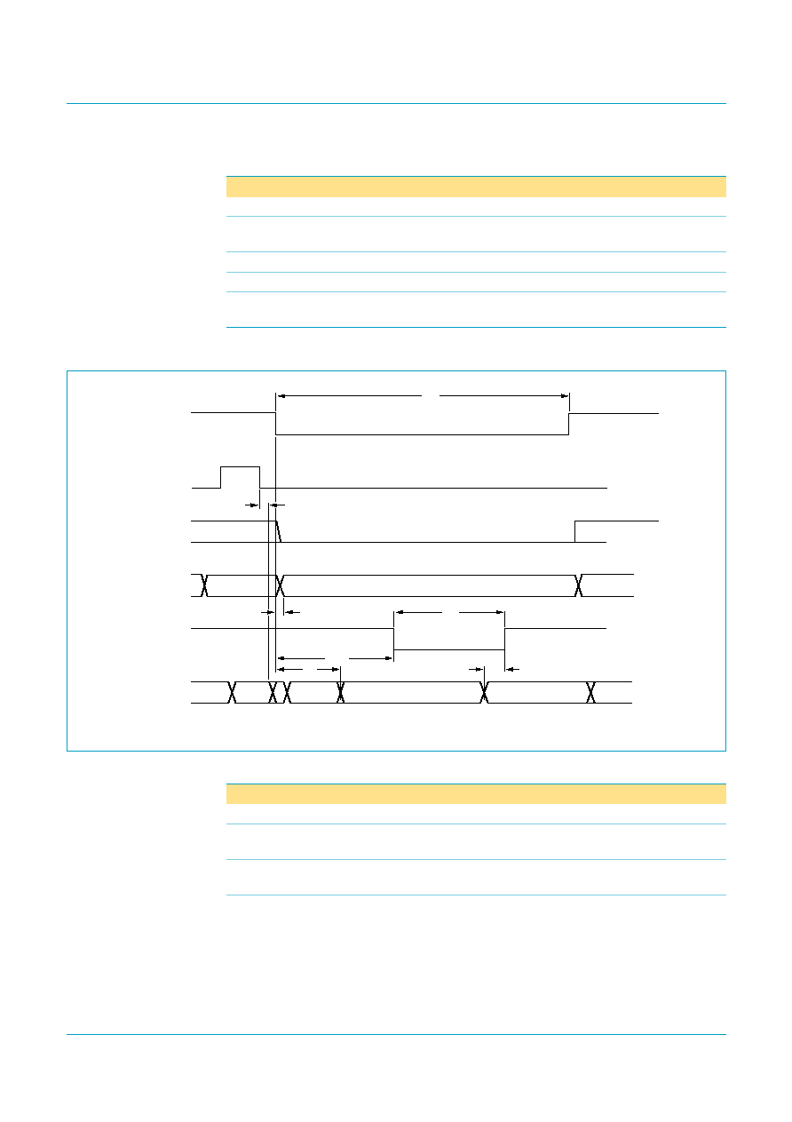
9.2.2
Interface connection
9.3 FEC interface
This is a serial interface for communication to a special front-end IC.
The timing diagram of the FEC interface is given in
Figure 41
. The first bit of a sector
is indicated by the sync signal; this is the MSB bit of the first byte of the header. The
sector error indication is in FEC mode indicated by two extra bytes at the end of the
sector. This means that the sector length is increased to 2066 bytes. The indication of
errors is as follows:
FF = error; 00 = no error.
Fig 40. Front-end interface connection.
MCE056
B_DATA
Be_dat(7:1)
Data_req
UDE_req
45
B_FLAG
42
B_SYNC
43
B_WCLK
44
B_BCLK
46
sdclk
req
49-55
senb
sync
serr
data
sdclk
UDE
front-end IC
senb
sync
serr
48
47
req
data
SAA7893HL
DVD
back-end IC
with UDE
Fig 41. FEC interface.
MBL619
bclk/
ser_bclk
be_dat(0)/
ser_data
wclk/
ser_valid
sync/
ser_sync
bit
2
bit
1
bit
4
bit
3
bit
6
bit
5
bit
8
bit
7
bit
10
bit
9
bit
12
bit
11
bit
14
bit
13
bit
16
bit
15

Philips Semiconductors
SAA7893HL
Super audio media player
Product data
Rev. 02 -- 26 February 2003
44 of 66
9397 750 10925
© Koninklijke Philips Electronics N.V. 2003. All rights reserved.
9.3.1
Timing
9.3.2
Interface connection
10. HF input
10.1 General
On every SACD disc a PSP signal must be recorded. The player is only allowed to
play a disc if a valid PSP signal is detected. This PSP key is recorded via a special
mechanism in the EFM signal on disc. The EFM+ signal must be fed to the
SAA7893HL as shown in
Figure 44
.
Fig 42. Timing in FEC interface.
MBL624
B_BCLK
tsu
th
B_SYNC
B_FLAG
B_WCLK
B_DATA
Table 26:
Timing in FEC interface
Symbol
Parameter
Min
Unit
t
su
set-up time to rising edge of the clock
10
ns
t
h
hold time after rising edge of the clock
5
ns
Fig 43. Front-end interface connection.
MCE057
B_DATA
45
B_FLAG
42
GND_IO
B_SYNC
43
B_WCLK
44
B_BCLK
46
Be_dat(7:1)
49-55
UDE_req
47
open
Data_req
48
ser_clk
FEC
front-end IC
ser_valid
ser_sync
ser_dat
SAA7893HL

Philips Semiconductors
SAA7893HL
Super audio media player
Product data
Rev. 02 -- 26 February 2003
45 of 66
9397 750 10925
© Koninklijke Philips Electronics N.V. 2003. All rights reserved.
The detection of the PSP key is dependent of the polarity of the EFM+ signal. The
SA-MP settings are that a pit on the disc must have a higher output voltage than the
land. The EFM+ input signal has no timing requirements with respect to the digital
input of the front-end interface of the SAA7893HL.
The SAA7893HL supports also an inversion of the EFM+ signal.
10.2 HF input specification
The AGC circuit must be able to handle the following signal characteristics of the
HF input signal.
The HF is AC-coupled via a capacitor of 10 nF to pin Agcinp. The internal resistance
of pin Agcinp is 1 M
.
Fig 44. Connection of EFM+ input.
Agcinp
EFM
+
VDDA
10 nF
100 nF
12 k
+
1.8 V
VSSA
MBL620
Adcrefl
biasin
Table 27:
HF signal characteristics
HF
Value
Remark
Input range
0.2 to 0.8 V (p-p)
HF input voltage
Bandwidth
9 MHz
front-end running on
maximum speed needed for
SACD
Table 28:
Signal connections
Pin name
Description
Agcinp
HF output from pickup unit connected via a 10 nF couple capacitor
biasin
bias current; connect a 12 k
resistor to V
SS
(ground)
Adcrefl
reference voltage for internal resistor trap; decouple with 100 nF to V
SS
(ground)
V
SSA
analog ground
V
DDA
1.8 V analog power supply

Philips Semiconductors
SAA7893HL
Super audio media player
Product data
Rev. 02 -- 26 February 2003
46 of 66
9397 750 10925
© Koninklijke Philips Electronics N.V. 2003. All rights reserved.
10.3 HF-input application diagram
11. Audio interfaces
11.1 Audio input interface
The PCM-I
2
S audio input signals can be either directly couple, without any
processing to the DSD_PCM output lines, or further processed inside the
SAA7893HL. When directly coupled, only a combinatorial delay must be taken into
account; no dependency on any clock signal (see
Section 11.1.1
). The input signal
characteristics, when audio processing must be performed, are given in
Section 11.1.2
.
11.1.1
Audio input directly coupled
When no processing is done inside the SAA7893HL with respect to the I
2
S-PCM
input stream, this input stream is sent via a multiplexer to the I
2
S-bus output paths. So
no clocking is done on this signal, meaning that also no locked audio clock needs to
be present.
Fig 45. EFM input interface connection.
Agcinp
EFM
+
(0.2-0.8 V)
VDDA
10 nF
4.7
µ
F
35
32
33
36
34
100 nF
100
nF
12 k
+
1.8 V
VSSA
MCE058
Adcrefl
SAA7893HL
biasin
Fig 46. Delay from input to output pin.
MBL627
input pin
output pin
td(as)
Table 29:
Timing numbers in PCM audio
Symbol
Parameter
Min
Typ
Max
Unit
t
d(as)
asynchronous delay
8
13
18
ns

Philips Semiconductors
SAA7893HL
Super audio media player
Product data
Rev. 02 -- 26 February 2003
47 of 66
9397 750 10925
© Koninklijke Philips Electronics N.V. 2003. All rights reserved.
11.1.2
Audio input `with processing'
11.1.3
Interface connection
11.2 Audio output interface
The 6-channel outputs can be either DSD format or PCM-I
2
S format. The
connections are given in
Table 31
.
Fig 47. Audio I
2
S-bus input timing.
MSB
right channel
right surround
LFE
16/24/32/48 clock cycles
PCM_wclk_in
PCM_dclk_in
PCM_LeRi_in
PCM_LsRs_in
PCM_CeLf_in
left channel
left surround
center
3
2
22
1
MSB
LSB
3
2
1
MBL628
tsu
th
24 data bits
tsu
th
Table 30:
Timing numbers in PCM audio
Symbol
Parameter
Conditions
Min
Unit
t
su
set-up time to rising edge to the
pcm_dclk_in signal
in PCM-I
2
S mode, the data is always outputted on
the negative edge of the bit clock; so here data is
sampled on positive edge of the clock
8
ns
t
h
hold time after rising edge of the
pcm_dclk_in signal
in PCM-I
2
S mode, the data is always outputted on
the negative edge of the bit clock; so here data is
sampled on positive edge of the clock
5
ns
Fig 48. Audio I
2
S-PCM input interface connection.
MCE059
PCM_CeLf_in
39
PCM_LsRs_in
41
PCM_LeRi_in
40
PCM_wclk_in
31
PCM_dclk_in
30
aud_clk
29
aud_clk_in
DVD
back-end IC
audio clock
256/384/512/768 x fs
I2S_clk
I2S_wclk
I2S_leri
I2S_Celfe
I2S_Isrs
SAA7893HL

Philips Semiconductors
SAA7893HL
Super audio media player
Product data
Rev. 02 -- 26 February 2003
48 of 66
9397 750 10925
© Koninklijke Philips Electronics N.V. 2003. All rights reserved.
The SAA7893HL has 12 output lines: 8 lines are allocated for connection to a
6-channel DAC and 4 are for connection to a 2-channel DAC or a 75 Hz reference
signal. The DSD data on the MCH output lines are outputted 6412 clocks after the
positive edge of the 75 Hz signal, if no additional post-processing is done.
The SA-MP delivers extra flexibility when connecting to different DAC types, which
can be: DSD only, PCM only or multi standard (DSD + PCM)]. In
Table 31
the signal
allocation is given for the 6-channel output in DSD and in PCM-I
2
S mode.
In
Table 32
the signal allocation is given for the DSD/PCM signals to be connected to
the stereo DAC.
Fig 49. SA-MP output line allocation.
DSD_PCM_0
DSD_PCM_1
DSD_PCM_2
DSD_PCM_3
DSD_PCM_4
DSD_PCM_5
to 6-channel DAC
to 2-channel DAC
DSD_PCM_6
DSD_PCM_7
SA-MP
DSD_PCM_8
DSD_PCM_9
DSD_PCM_10
DSD_PCM_11
MBL621
Table 31:
Connection to a 6-channel DAC
Output line
Pin
number
Mode = DSD
Mode = PCM
DSD_PCM_0
108
left channel
L
f
+ R
f
; L
s
+ R
s
; C + LFE; 0 or 1;
PCM data/word clock
DSD_PCM_1
109
right channel
L
f
+ R
f
; L
s
+ R
s
; C + LFE; 0 or 1;
PCM data/word clock
DSD_PCM_2
110
center channel
L
f
+ R
f
; L
s
+ R
s
; C + LFE; 0 or 1;
PCM data/word clock
DSD_PCM_3
111
LFE channel
L
f
+ R
f
; L
s
+ R
s
; C + LFE; 0 or 1;
PCM data/word clock
DSD_PCM_4
113
left surround
L
f
+ R
f
; L
s
+ R
s
; C + LFE; 0 or 1;
PCM data/word clock
DSD_PCM_5
114
right surround
L
f
+ R
f
; L
s
+ R
s
; C + LFE; 0 or 1;
PCM data/word clock
DSD_PCM_6
115
DSD clock or
0 or 1
PCM data/word clock
DSD_PCM_7
116
DSD clock or
0 or 1
PCM data/word clock

Philips Semiconductors
SAA7893HL
Super audio media player
Product data
Rev. 02 -- 26 February 2003
49 of 66
9397 750 10925
© Koninklijke Philips Electronics N.V. 2003. All rights reserved.
Both tables show that DSD has a fixed allocation while PCM outputs are selectable.
The I
2
S-bus bit stream, generated by the SAA7893HL decimation filter, is in the
Philips format as can be seen in the timing diagrams. The number of data bits is
always 24.
The wclk identification is always active for 32 clocks for each left and right sample,
except when the input clock is 384f
s
and the output sample frequency is 4f
s
; then the
wclk is 48 samples active.
11.2.1
DSD output
Remark: in this example timing of the aud_clk is 256
◊
f
s
and DSD clock phase is set
to logic 0. If phase is set to logic 1, the dsd_clk signal will be inverted.
Table 32:
Connection to a 4-channel DAC
Output line
Pin
number
Mode = DSD
Mode = PCM
Mode = 75 Hz
DSD_PCM_8
117
DSD clock
PCM data/word clock
0 or 1
DSD_PCM_9
120
0 or 1
PCM data/word clock
0 or 1
DSD_PCM_10
119
left channel
L
f
+ R
f
; 0 or 1
75 Hz
DSD_PCM_11
121
right channel
L
f
+ R
f
; 0 or 1
0 or 1
Table 33:
Serial bit clock frequency
Audio input
clock
I
2
S output `wclk'
frequency
DCLK (data bit)
frequency
Remark
256f
s
2f
s
128f
s
4f
s
256f
s
384f
s
2f
s
128f
s
no symmetrical bit clock
4f
s
384f
s
48 clocks for a word
identification
512f
s
2f
s
128f
s
4f
s
256f
s
768f
s
2f
s
128f
s
4f
s
256f
s
Fig 50. Audio I
2
S-bus output timing.
MBL629
dsd_clk (= 64fs)
aud_clk
dsd_pcm-data
SAMPLE N
SAMPLE N + 1
td(o)

Philips Semiconductors
SAA7893HL
Super audio media player
Product data
Rev. 02 -- 26 February 2003
50 of 66
9397 750 10925
© Koninklijke Philips Electronics N.V. 2003. All rights reserved.
11.2.2
I
2
S-PCM generated by the SAA7893HL
In
Figure 51
and
Figure 52
the timing diagrams are given when the internal PCM
generator of the SAA7893HL generates the I
2
S-PCM output signals.
Table 34:
Timing numbers in DSD audio
Symbol
Parameter
Min
Max
Unit
t
d(o)
output delay time with respect to the audio clock
4
20
ns
Fig 51. Audio I
2
S-bus output timing in Philips format.
MSB
right channel
right surround
LFE
32 pcm_dclk_out clock cycles
pcm_wclk_out
pcm_dclk_out
pcm_LeRi_out
pcm_LsRs_out
pcm_CeLf_out
left channel
left surround
center
3
2
22
1
MSB
LSB
3
2
1
MBL630
tdata
24 data bits
twclk
Fig 52. Audio I
2
S-bus output timing in left justified format.
left channel
left surround
center
32 clock cycles
right channel
right surround
LFE
3
2
22
1
MSB
LSB
3
2
1
MBL631
tdata
24 data bits
twclk
MSB
Table 35:
Timing numbers for PCM-I
2
S output
Symbol
Parameter
Min
Max
Unit
t
wclk
pcm_wclk_out timing with respect to negative
edge of pcm_dclk_out
-
10
+10
ns
t
data
pcm_data_out timing with respect to negative
edge of pcm_dclk_out
-
10
+10
ns

Philips Semiconductors
SAA7893HL
Super audio media player
Product data
Rev. 02 -- 26 February 2003
51 of 66
9397 750 10925
© Koninklijke Philips Electronics N.V. 2003. All rights reserved.
11.3 Audio output application diagrams
11.3.1
Hybrid DAC connection
Fig 53. Hybrid DAC interface connection.
MCE060
sdata_Isrs
M_x
sclk
wclk
113
sclk
wclk
sdata_Ifrf
M_x
114
M_x
111
sdata_celfe
110
M_x
109
sdata_ifrf
108
DSD_PCM_0
dsd_left/
i2s_lfrf
dsd_clk/
i2s_dclk
dsd_clk/
i2s_dclk
'0'/
i2s_wclk
'0'/
i2s_wclk
dsd_left_sur/
i2s_lsrs
dsd_left_mix/
i2s_lmrm
dsd_right_mix/
'0'
dsd_right_sur/
'0'
dsd_right/
'0'
dsd_centre/
i2s_celfe
hybrid
MCA DAC
hybrid
stereo DAC
mclk
aud_clk
mclk
all slew rate
controlled
output pins
(no serial
resistors needed)
audio clock
DSD_PCM_1
DSD_PCM_2
DSD_PCM_3
DSD_PCM_4
DSD_PCM_5
116
115
DSD_PCM_6
DSD_PCM_7
117
DSD_PCM_8
119
121
29
120
DSD_PCM_9
DSD_PCM_10
DSD_PCM_11
SAA7893HL
dsd_lfe/
'0'

Philips Semiconductors
SAA7893HL
Super audio media player
Product data
Rev. 02 -- 26 February 2003
52 of 66
9397 750 10925
© Koninklijke Philips Electronics N.V. 2003. All rights reserved.
11.3.2
DSD DAC connection
Fig 54. DSD DAC interface connection.
MCE061
dsd_ls
dsd_rs
sclk
n.c.
n.c.
113
dsd_clk
dsd_left
dsd_right
114
dsd_lfe
111
dsd_centre
110
dsd_right
109
dsd_left
108
DSD_PCM_0
dsd_left
dsd_clk
dsd_clk
dsd_left_sur
dsd_left_mix
dsd_right_mix
dsd_right_sur
dsd_right
dsd_centre
DSD
MCA DAC
DSD
stereo DAC
mclk
aud_clk
mclk
audio clock
DSD_PCM_1
DSD_PCM_2
DSD_PCM_3
DSD_PCM_4
DSD_PCM_5
116
115
DSD_PCM_6
DSD_PCM_7
117
DSD_PCM_8
119
121
29
120
DSD_PCM_9
DSD_PCM_10
DSD_PCM_11
SAA7893HL
dsd_lfe

Philips Semiconductors
SAA7893HL
Super audio media player
Product data
Rev. 02 -- 26 February 2003
53 of 66
9397 750 10925
© Koninklijke Philips Electronics N.V. 2003. All rights reserved.
11.3.3
PCM DAC connection
Fig 55. PCM DAC interface connection.
MCE062
sdata_lsrs
sclk
wclk
n.c.
n.c.
n.c.
n.c.
113
sclk
sdata_lfrf
wclk
114
111
sdata_celfe
110
109
sdata_lfrf
108
DSD_PCM_0
i2s_lfrf
i2s_dclk
i2s_wclk
i2s_dclk
i2s_lsrs
i2s_lmrm
i2s_wclk
i2s_celfe
PCM
MCA DAC
PCM
stereo DAC
mclk
aud_clk
mclk
audio clock
DSD_PCM_1
DSD_PCM_2
DSD_PCM_3
DSD_PCM_4
DSD_PCM_5
116
115
DSD_PCM_6
DSD_PCM_7
117
DSD_PCM_8
119
121
29
120
DSD_PCM_9
DSD_PCM_10
DSD_PCM_11
SAA7893HL

Philips Semiconductors
SAA7893HL
Super audio media player
Product data
Rev. 02 -- 26 February 2003
54 of 66
9397 750 10925
© Koninklijke Philips Electronics N.V. 2003. All rights reserved.
12. SDRAM interface
12.1 Writing
Fig 56. SDRAM interface writing.
active
write
address
address
data
ZZZZ
ZZZZ
XX
XX
upper/lower
byte
precharge
nop
clk
D_clk
D_ADDR[13:0]
D_DQ[15:0]
D_RASn
D_CASn
D_Wen
D_UDQM
D_LDQM
MBL632
td
tcmd
taddr
tdata
tdqm
Table 36:
Timing numbers of SDRAM interface writing
Symbol
Parameter
Conditions
Min
Max
Unit
t
d
delay from clk to D_clk of SDRAM interface
D_clk is clock of SDRAM
3
9
ns
t
cmd
delay from clk to control signals
1
15
ns
t
addr
delay from clk to address lines
1
15
ns
t
dqm
delay from clk to D_UDQM and D_LDQM
signals
1
12
ns
t
data
delay from clk to data output signals
1
12
ns

Philips Semiconductors
SAA7893HL
Super audio media player
Product data
Rev. 02 -- 26 February 2003
55 of 66
9397 750 10925
© Koninklijke Philips Electronics N.V. 2003. All rights reserved.
12.2 Reading
Fig 57. SDRAM interface reading.
data to
SAA7893HL
active
address
address
upper/lower
byte
read
nop
nop
nop
precharge
nop
clk
D_clk
D_ADDR[13:0]
D_DQ[15:0]
D_RASn
D_CASn
D_Wen
D_UDQM
D_LDQM
MBL634
td
tcmd
taddr
tdqm
th
tsu
Table 37:
Timing numbers of SDRAM interface reading
Symbol
Parameter
Conditions
Min
Max
Unit
t
d
delay from clk to D_clk of SDRAM interface
D_clk is clock of SDRAM
3
9
ns
t
cmd
delay from clk to control signals
1
15
ns
t
addr
delay from clk to address lines
1
15
ns
t
dqm
delay from clk to D_UDQM and D_LDQM
signals
1
12
ns
t
su
set-up time of data to clk
3
-
ns
t
h
hold time of data from clk
3
-
ns

Philips Semiconductors
SAA7893HL
Super audio media player
Product data
Rev. 02 -- 26 February 2003
56 of 66
9397 750 10925
© Koninklijke Philips Electronics N.V. 2003. All rights reserved.
12.3 Interface connection
Fig 58. SDRAM interface connection.
MCE063
BA1
75
RAS_
81
BA0
78
A(11:0)
DQ(15:0)
DQMH
88
DQML
89
CS_
CLK
86
WE_
80
CAS_
82
CKE
64 Mbit SDRAM
+3.3 V
D_DQ[15:0]
D_ADDR[11:0]
D_ADDR[12]
D_ADDR[13]
D_RASn
D_CASn
D_Wen
D_clk
D_UDQM
D_LDQM
SAA7893HL

Philips Semiconductors
SAA7893HL
Super audio media player
Product data
Rev. 02 -- 26 February 2003
57 of 66
9397 750 10925
© Koninklijke Philips Electronics N.V. 2003. All rights reserved.
13. Power supply connections
Fig 59. Power supply connections.
MCE064
10
VCC_IO1
3.3 to 1.8 V
CONVERTOR
(LF18CD)
100 MHz
coil
GND_IO1
VCC_IO7
GND_IO7
VCC_IO2
GND_IO2
VCC_IO3
GND_IO3
VCC_IO4
GND_IO4
VCC_IO5
GND_IO5
VCC_IO6
GND_IO6
38
4
37
100
nF
SAA7893HL
100
nF
17
58
100
nF
69
76
100
nF
83
92
100
nF
99
106
100
nF
100
nF
4.7
µ
F
100
nF
4.7
µ
F
4.7
µ
F
112
118
100
nF
VCC_Core1
GND_Core1
VCC_Core2
GND_Core2
20
19
100
nF
3.3 V
84
85
100
nF
VSSA
VDDA
33
32
100
nF
100 MHz
coil
4.7
µ
F
3.3 to 1.8 V
CONVERTOR
(LF18CD)
100
nF
4.7
µ
F

Philips Semiconductors
SAA7893HL
Super audio media player
Product data
Rev. 02 -- 26 February 2003
58 of 66
9397 750 10925
© Koninklijke Philips Electronics N.V. 2003. All rights reserved.
14. Software API
14.1 API provided by SA-MP
Table 38:
API provided by SA-MP
Name
Description
Playback API
NAV_AreaSwitch
Switch SACD Area
NAV_PlayTrack
Start playing at the index of the track
NAV_PlayAtTimecode
Start playing at the given time
NAV_Stop
Stop playback
NAV_Pause
Pause playback
NAV_ResumePlay
Resume playback at normal speed
NAV_NextTrack
Continue with next track
NAV_PreviousTrack
Continue with previous track
NAV_Repeat
Set the repeat mode for playback
NAV_RepeatAB
Set the repeat AB mode
NAV_Shuffle
Play tracks in random order
NAV_IntroScan
Play only intro part of each track
NAV_ForwardScan
Start scanning forward ≠ fast playback with burst sound
NAV_BackwardScan
Start scanning backward ≠ fast playback with burst
sound
NAV_SetPlaySequence
Set play sequence mode
NAV_SetProgramList
Set program list
NAV_GetState
Returns navigator states
NAV_GetPlayList
Returns navigator play list
Post-processing API
APM_SetSpeakers
Select speaker configuration
APM_SetInputMode
Select between DSD or PCM as APM input
APM_SetOutputMode
Select APM output mode (DSD or PCM)
APM_Set6chDownMix
Set the downmix of six-channel output stream
APM_Set2chDownMix
Set the downmix of two-channel output stream
APM_SetBassFilters
Select the bass management frequency and slope
APM_SetAttenuation
Set attenuation of an output channel
APM_SetDelay
Set delay of a channel of output stream
APM_SetFilterMode
Set Sigma Delta modulator filter mode
APM_SetPcmUpsampling
Set the PCM upsampling mode
APM_SetPIO
Set the DAC PIO pins
Text and Data API
SDI_SetAvailableCharSets
Set a list of character sets, application can handle
SDI_SetLanguagePreference
Set a list of preferred languages
SDI_GetAlbumInfo
Retrieve information about the album of active disc
SDI_GetAlbumText
Retrieve album text items

Philips Semiconductors
SAA7893HL
Super audio media player
Product data
Rev. 02 -- 26 February 2003
59 of 66
9397 750 10925
© Koninklijke Philips Electronics N.V. 2003. All rights reserved.
14.2 API required by SA-MP
Software to be provided by the DVD host:
∑
For the front-end: Seek, GetDataArea, TransferRate (optional)
∑
For the operating system: Tasks, Interrupts, Semaphores, Mailboxes, Timers.
SDI_GetNumberOfIndices
Retrieve number of indices for specified track
SDI_GetDiscInfo
Retrieve information about the active disc
SDI_GetDiscText
Retrieve disc text items
SDI_GetAreaText
Retrieve area text items
SDI_GetTrackInfo
Retrieve information about the specified track
SDI_GetTrackText
Retrieve track text items
System configuration API
SDM_SetBeType
Select the front-end interface attached to SA-MP
SDM_SetDacPinnning
Configure the DAC pins
SDM_SetAudioClock
Configure the audio clock for different input stream
modes
SDM_SetMemoryConfig
Configure the SDRAM attached to the SAA7893HL
SDM_GetHandler
Return the pointer to SA-MP interrupt handler
SDM_SetDsdClockPolarity
Configure the DSD clock polarity
SDM_SetSystemClock
Inform SA-MP about the system clock
SDM_SetBurstLength
Configure the burst length for fast play
General API
SAMP_Init
Initialize SA-MP
SAMP_Term
Terminate SA-MP
SAMP_Activate
Activate SA-MP
SAMP_Reactivate
Reactivate SA-MP
SAMP_Deactivate
Deactivate SA-MP
SAMP_SACDDiscReq
SACD disc recognition
Table 38:
API provided by SA-MP
...continued
Name
Description

Philips Semiconductors
SAA7893HL
Super audio media player
Product data
Rev. 02 -- 26 February 2003
60 of 66
9397 750 10925
© Koninklijke Philips Electronics N.V. 2003. All rights reserved.
15. Limiting values
[1]
Stresses above the absolute maximum ratings may cause permanent damage to the device. Exposure to absolute maximum ratings for
extended periods may effect device reliability.
16. Characteristics
Table 39:
Absolute maximum ratings
In accordance with the Absolute Maximum Rating System (IEC 60134). Note
1
.
Symbol
Parameter
Min
Max
Unit
VCC_Core
digital core supply voltage
-
0.5
+
2.1
V
VCC_IO
IO pins supply voltage
-
0.5
+
3.8
V
V
DDA
analog supply voltage
-
0.5
+
2.1
V
V
I
DC input voltage
-
0.5
+
5.5
V
T
amb
ambient temperature
0
70
∞
C
T
stg
storage temperature
-
25
+
125
∞
C
T
j
junction temperature
-
150
+
150
∞
C
Table 40:
Characteristics
Symbol
Parameter
Min
Typ
Max
Unit
Power supply: VCC_Core (digital core supply voltage)
VCC_Core
digital core supply voltage
1.65
1.8
1.95
V
P
power dissipation
90
110
150
mW
Power supply: V
DDA
(analog supply voltage)
V
DDA
analog supply voltage
1.65
1.8
1.95
V
P
power dissipation during disc recognition only
-
40
60
mW
Power supply: VCC_IO (I/O pins supply voltage)
VCC_IO
I/O pins supply voltage
3.0
3.3
3.6
V
P
power dissipation during disc recognition only
-
70
100
mW
Digital inputs and outputs
V
IH
HIGH-level input voltage
2.0
-
VCC_IO + 0.5 V
V
IL
LOW-level input voltage
-
-
0.8
V
V
OH
HIGH-level output voltage
VCC_IO
-
0.4 -
-
V
V
OL
LOW-level output voltage
-
-
0.4
V
C
i
input capacitance
-
-
10
pF
C
o
output capacitance
-
-
10
pF
I
LI
input leakage current
-
-
±
10
µ
A
I
i(n)
input current on any pin except supplies
-
-
±
10
mA

Philips Semiconductors
SAA7893HL
Super audio media player
Product data
Rev. 02 -- 26 February 2003
61 of 66
9397 750 10925
© Koninklijke Philips Electronics N.V. 2003. All rights reserved.
17. Package outline
Fig 60. LQFP128 (SOT425-1) package outline.
UNIT
A
1
A
2
A
3
b
p
c
E
(1)
e
H
E
L
L
p
Z
y
w
v
REFERENCES
OUTLINE
VERSION
EUROPEAN
PROJECTION
ISSUE DATE
IEC
JEDEC
EIAJ
mm
0.15
0.05
1.45
1.35
0.25
0.27
0.17
0.20
0.09
14.1
13.9
0.5
16.15
15.85
0.81
0.59
7
0
o
o
0.12
0.2
0.1
1.0
DIMENSIONS (mm are the original dimensions)
Note
1. Plastic or metal protrusions of 0.25 mm maximum per side are not included.
0.75
0.45
SOT425-1
136E28
MS-026
99-12-27
00-01-19
D
(1)
(1)
(1)
20.1
19.9
H
D
22.15
21.85
E
Z
0.81
0.59
D
0
5
10 mm
scale
b
p
e
E
A
1
A
L
p
detail X
L
(A )
3
B
c
b
p
E
H
A
2
D
H
v
M
B
D
Z D
A
Z E
e
v
M
A
X
102
103
y
w
M
w
M
A
max.
1.6
LQFP128: plastic low profile quad flat package; 128 leads; body 14 x 20 x 1.4 mm
SOT425-1
65
64
38
39
1
128
pin 1 index

Philips Semiconductors
SAA7893HL
Super audio media player
Product data
Rev. 02 -- 26 February 2003
62 of 66
9397 750 10925
© Koninklijke Philips Electronics N.V. 2003. All rights reserved.
18. Soldering
18.1 Introduction to soldering surface mount packages
This text gives a very brief insight to a complex technology. A more in-depth account
of soldering ICs can be found in our
Data Handbook IC26; Integrated Circuit
Packages (document order number 9398 652 90011).
There is no soldering method that is ideal for all surface mount IC packages. Wave
soldering can still be used for certain surface mount ICs, but it is not suitable for fine
pitch SMDs. In these situations reflow soldering is recommended.
18.2 Reflow soldering
Reflow soldering requires solder paste (a suspension of fine solder particles, flux and
binding agent) to be applied to the printed-circuit board by screen printing, stencilling
or pressure-syringe dispensing before package placement.
Several methods exist for reflowing; for example, convection or convection/infrared
heating in a conveyor type oven. Throughput times (preheating, soldering and
cooling) vary between 100 and 200 seconds depending on heating method.
Typical reflow peak temperatures range from 215 to 250
∞
C. The top-surface
temperature of the packages should preferably be kept:
∑
below 220
∞
C for all the BGA packages and packages with a thickness
2.5mm
and packages with a thickness <2.5 mm and a volume
350 mm
3
so called
thick/large packages
∑
below 235
∞
C for packages with a thickness <2.5 mm and a volume <350 mm
3
so
called small/thin packages.
18.3 Wave soldering
Conventional single wave soldering is not recommended for surface mount devices
(SMDs) or printed-circuit boards with a high component density, as solder bridging
and non-wetting can present major problems.
To overcome these problems the double-wave soldering method was specifically
developed.
If wave soldering is used the following conditions must be observed for optimal
results:
∑
Use a double-wave soldering method comprising a turbulent wave with high
upward pressure followed by a smooth laminar wave.
∑
For packages with leads on two sides and a pitch (e):
≠ larger than or equal to 1.27 mm, the footprint longitudinal axis is preferred to be
parallel to the transport direction of the printed-circuit board;
≠ smaller than 1.27 mm, the footprint longitudinal axis must be parallel to the
transport direction of the printed-circuit board.
The footprint must incorporate solder thieves at the downstream end.

Philips Semiconductors
SAA7893HL
Super audio media player
Product data
Rev. 02 -- 26 February 2003
63 of 66
9397 750 10925
© Koninklijke Philips Electronics N.V. 2003. All rights reserved.
∑
For packages with leads on four sides, the footprint must be placed at a 45
∞
angle
to the transport direction of the printed-circuit board. The footprint must
incorporate solder thieves downstream and at the side corners.
During placement and before soldering, the package must be fixed with a droplet of
adhesive. The adhesive can be applied by screen printing, pin transfer or syringe
dispensing. The package can be soldered after the adhesive is cured.
Typical dwell time is 4 seconds at 250
∞
C. A mildly-activated flux will eliminate the
need for removal of corrosive residues in most applications.
18.4 Manual soldering
Fix the component by first soldering two diagonally-opposite end leads. Use a low
voltage (24 V or less) soldering iron applied to the flat part of the lead. Contact time
must be limited to 10 seconds at up to 300
∞
C.
When using a dedicated tool, all other leads can be soldered in one operation within
2 to 5 seconds between 270 and 320
∞
C.
18.5 Package related soldering information
[1]
For more detailed information on the BGA packages refer to the
(LF)BGA Application Note
(AN01026); order a copy from your Philips Semiconductors sales office.
[2]
All surface mount (SMD) packages are moisture sensitive. Depending upon the moisture content, the
maximum temperature (with respect to time) and body size of the package, there is a risk that internal
or external package cracks may occur due to vaporization of the moisture in them (the so called
popcorn effect). For details, refer to the Drypack information in the
Data Handbook IC26; Integrated
Circuit Packages; Section: Packing Methods.
[3]
These packages are not suitable for wave soldering. On versions with the heatsink on the bottom
side, the solder cannot penetrate between the printed-circuit board and the heatsink. On versions with
the heatsink on the top side, the solder might be deposited on the heatsink surface.
[4]
If wave soldering is considered, then the package must be placed at a 45
∞
angle to the solder wave
direction. The package footprint must incorporate solder thieves downstream and at the side corners.
[5]
Wave soldering is suitable for LQFP, QFP and TQFP packages with a pitch (e) larger than 0.8 mm; it
is definitely not suitable for packages with a pitch (e) equal to or smaller than 0.65 mm.
[6]
Wave soldering is suitable for SSOP and TSSOP packages with a pitch (e) equal to or larger than
0.65 mm; it is definitely not suitable for packages with a pitch (e) equal to or smaller than 0.5 mm.
Table 41:
Suitability of surface mount IC packages for wave and reflow soldering
methods
Package
[1]
Soldering method
Wave
Reflow
[2]
BGA, LBGA, LFBGA, SQFP, TFBGA, VFBGA
not suitable
suitable
DHVQFN, HBCC, HBGA, HLQFP, HSQFP,
HSOP, HTQFP, HTSSOP, HVQFN, HVSON,
SMS
not suitable
[3]
suitable
PLCC
[4]
, SO, SOJ
suitable
suitable
LQFP, QFP, TQFP
not recommended
[4][5]
suitable
SSOP, TSSOP, VSO, VSSOP
not recommended
[6]
suitable

Philips Semiconductors
SAA7893HL
Super audio media player
Product data
Rev. 02 -- 26 February 2003
64 of 66
9397 750 10925
© Koninklijke Philips Electronics N.V. 2003. All rights reserved.
19. Revision history
Table 42:
Revision history
Rev Date
CPCN
Description
02
20030226
-
Product data (9397 750 10925)
Modifications:
∑
The value of the capacitor to pin Adcrefl in
Figure 44
is changed from 10 nF to 100 nF
∑
The system clock definitions are added in
Section 7.5.1
∑
The audio clock definitions are added in
Section 7.5.2
∑
A remark is added at the end of
Section 8.2
.
∑
A note is added to
Table 11
.
01
20021014
-
Product data (9397 750 10341)

9397 750 10925
Philips Semiconductors
SAA7893HL
Super audio media player
© Koninklijke Philips Electronics N.V. 2003. All rights reserved.
Product data
Rev. 02 -- 26 February 2003
65 of 66
Contact information
For additional information, please visit http://www.semiconductors.philips.com.
For sales office addresses, send e-mail to: sales.addresses@www.semiconductors.philips.com.
Fax: +31 40 27 24825
20. Data sheet status
[1]
Please consult the most recently issued data sheet before initiating or completing a design.
[2]
The product status of the device(s) described in this data sheet may have changed since this data sheet was published. The latest information is available on the Internet at
URL http://www.semiconductors.philips.com.
[3]
For data sheets describing multiple type numbers, the highest-level product status determines the data sheet status.
21. Definitions
Short-form specification -- The data in a short-form specification is
extracted from a full data sheet with the same type number and title. For
detailed information see the relevant data sheet or data handbook.
Limiting values definition -- Limiting values given are in accordance with
the Absolute Maximum Rating System (IEC 60134). Stress above one or
more of the limiting values may cause permanent damage to the device.
These are stress ratings only and operation of the device at these or at any
other conditions above those given in the Characteristics sections of the
specification is not implied. Exposure to limiting values for extended periods
may affect device reliability.
Application information -- Applications that are described herein for any
of these products are for illustrative purposes only. Philips Semiconductors
make no representation or warranty that such applications will be suitable for
the specified use without further testing or modification.
22. Disclaimers
Life support -- These products are not designed for use in life support
appliances, devices, or systems where malfunction of these products can
reasonably be expected to result in personal injury. Philips Semiconductors
customers using or selling these products for use in such applications do so
at their own risk and agree to fully indemnify Philips Semiconductors for any
damages resulting from such application.
Right to make changes -- Philips Semiconductors reserves the right to
make changes in the products - including circuits, standard cells, and/or
software - described or contained herein in order to improve design and/or
performance. When the product is in full production (status `Production'),
relevant changes will be communicated via a Customer Product/Process
Change Notification (CPCN). Philips Semiconductors assumes no
responsibility or liability for the use of any of these products, conveys no
licence or title under any patent, copyright, or mask work right to these
products, and makes no representations or warranties that these products are
free from patent, copyright, or mask work right infringement, unless otherwise
specified.
23. Trademarks
Dolby -- Available only to licensees of Dolby Laboratories Licensing
Corporation, San Francisco, CA94111, USA, from whom licensing and
application information must be obtained. Dolby is a registered trade-mark of
Dolby Laboratories Licensing Corporation.
Level
Data sheet status
[1]
Product status
[2][3]
Definition
I
Objective data
Development
This data sheet contains data from the objective specification for product development. Philips
Semiconductors reserves the right to change the specification in any manner without notice.
II
Preliminary data
Qualification
This data sheet contains data from the preliminary specification. Supplementary data will be published
at a later date. Philips Semiconductors reserves the right to change the specification without notice, in
order to improve the design and supply the best possible product.
III
Product data
Production
This data sheet contains data from the product specification. Philips Semiconductors reserves the
right to make changes at any time in order to improve the design, manufacturing and supply. Relevant
changes will be communicated via a Customer Product/Process Change Notification (CPCN).

© Koninklijke Philips Electronics N.V. 2003.
Printed in The Netherlands
All rights are reserved. Reproduction in whole or in part is prohibited without the prior
written consent of the copyright owner.
The information presented in this document does not form part of any quotation or
contract, is believed to be accurate and reliable and may be changed without notice. No
liability will be accepted by the publisher for any consequence of its use. Publication
thereof does not convey nor imply any license under patent- or other industrial or
intellectual property rights.
Date of release: 26 February 2003
Document order number: 9397 750 10925
Contents
Philips Semiconductors
SAA7893HL
Super audio media player
1
General description . . . . . . . . . . . . . . . . . . . . . . 1
1.1
Hardware . . . . . . . . . . . . . . . . . . . . . . . . . . . . . 2
1.2
Software . . . . . . . . . . . . . . . . . . . . . . . . . . . . . . 2
2
Features . . . . . . . . . . . . . . . . . . . . . . . . . . . . . . . 3
2.1
Components . . . . . . . . . . . . . . . . . . . . . . . . . . . 3
2.2
HW interfaces . . . . . . . . . . . . . . . . . . . . . . . . . . 3
2.3
SW interfaces . . . . . . . . . . . . . . . . . . . . . . . . . . 3
2.4
System . . . . . . . . . . . . . . . . . . . . . . . . . . . . . . . 4
2.5
System configuration . . . . . . . . . . . . . . . . . . . . 4
2.6
SACD playback. . . . . . . . . . . . . . . . . . . . . . . . . 4
2.7
Audio postprocessing . . . . . . . . . . . . . . . . . . . . 4
2.8
SACD data and text . . . . . . . . . . . . . . . . . . . . . 5
2.9
General . . . . . . . . . . . . . . . . . . . . . . . . . . . . . . . 5
3
Applications . . . . . . . . . . . . . . . . . . . . . . . . . . . . 5
4
Ordering information . . . . . . . . . . . . . . . . . . . . . 6
5
Block diagram . . . . . . . . . . . . . . . . . . . . . . . . . . 6
6
Pinning information . . . . . . . . . . . . . . . . . . . . . . 7
6.1
Pinning . . . . . . . . . . . . . . . . . . . . . . . . . . . . . . . 7
6.2
Pin description . . . . . . . . . . . . . . . . . . . . . . . . . 8
7
Interfaces . . . . . . . . . . . . . . . . . . . . . . . . . . . . . 11
7.1
Host interface . . . . . . . . . . . . . . . . . . . . . . . . . 11
7.2
Front-end interface . . . . . . . . . . . . . . . . . . . . . 11
7.3
Audio interface . . . . . . . . . . . . . . . . . . . . . . . . 12
7.4
SDRAM interface . . . . . . . . . . . . . . . . . . . . . . 12
7.5
Clock and reset input . . . . . . . . . . . . . . . . . . . 12
7.6
Test inputs. . . . . . . . . . . . . . . . . . . . . . . . . . . . 13
8
Host interface . . . . . . . . . . . . . . . . . . . . . . . . . . 14
8.1
General description. . . . . . . . . . . . . . . . . . . . . 14
8.2
SAD16_01/02 mode . . . . . . . . . . . . . . . . . . . . 15
8.3
SAD16_03 mode . . . . . . . . . . . . . . . . . . . . . . 19
8.4
MAD16_01 mode . . . . . . . . . . . . . . . . . . . . . . 25
8.5
MAD16_02 mode . . . . . . . . . . . . . . . . . . . . . . 30
8.6
SAD08 mode . . . . . . . . . . . . . . . . . . . . . . . . . 33
8.7
Interrupt . . . . . . . . . . . . . . . . . . . . . . . . . . . . . 37
9
Front-end interface . . . . . . . . . . . . . . . . . . . . . 37
9.1
I
2
S-bus interface . . . . . . . . . . . . . . . . . . . . . . . 38
9.2
UDE data interface . . . . . . . . . . . . . . . . . . . . . 40
9.3
FEC interface . . . . . . . . . . . . . . . . . . . . . . . . . 43
10
HF input . . . . . . . . . . . . . . . . . . . . . . . . . . . . . . 44
10.1
General . . . . . . . . . . . . . . . . . . . . . . . . . . . . . . 44
10.2
HF input specification . . . . . . . . . . . . . . . . . . . 45
10.3
HF-input application diagram . . . . . . . . . . . . . 46
11
Audio interfaces . . . . . . . . . . . . . . . . . . . . . . . . 46
11.1
Audio input interface . . . . . . . . . . . . . . . . . . . . 46
11.2
Audio output interface . . . . . . . . . . . . . . . . . . . 47
11.3
Audio output application diagrams . . . . . . . . . 51
12
SDRAM interface . . . . . . . . . . . . . . . . . . . . . . . 54
12.1
Writing . . . . . . . . . . . . . . . . . . . . . . . . . . . . . . 54
12.2
Reading . . . . . . . . . . . . . . . . . . . . . . . . . . . . . 55
12.3
Interface connection . . . . . . . . . . . . . . . . . . . . 56
13
Power supply connections . . . . . . . . . . . . . . . 57
14
Software API . . . . . . . . . . . . . . . . . . . . . . . . . . 58
14.1
API provided by SA-MP . . . . . . . . . . . . . . . . . 58
14.2
API required by SA-MP . . . . . . . . . . . . . . . . . 59
15
Limiting values . . . . . . . . . . . . . . . . . . . . . . . . 60
16
Characteristics . . . . . . . . . . . . . . . . . . . . . . . . 60
17
Package outline . . . . . . . . . . . . . . . . . . . . . . . . 61
18
Soldering . . . . . . . . . . . . . . . . . . . . . . . . . . . . . 62
18.1
Introduction to soldering surface mount
packages . . . . . . . . . . . . . . . . . . . . . . . . . . . . 62
18.2
Reflow soldering. . . . . . . . . . . . . . . . . . . . . . . 62
18.3
Wave soldering. . . . . . . . . . . . . . . . . . . . . . . . 62
18.4
Manual soldering . . . . . . . . . . . . . . . . . . . . . . 63
18.5
Package related soldering information . . . . . . 63
19
Revision history . . . . . . . . . . . . . . . . . . . . . . . 64
20
Data sheet status. . . . . . . . . . . . . . . . . . . . . . . 65
21
Definitions . . . . . . . . . . . . . . . . . . . . . . . . . . . . 65
22
Disclaimers . . . . . . . . . . . . . . . . . . . . . . . . . . . 65
23
Trademarks . . . . . . . . . . . . . . . . . . . . . . . . . . . 65